WO2024203522A1 - 積層セラミック電子部品 - Google Patents
積層セラミック電子部品 Download PDFInfo
- Publication number
- WO2024203522A1 WO2024203522A1 PCT/JP2024/010486 JP2024010486W WO2024203522A1 WO 2024203522 A1 WO2024203522 A1 WO 2024203522A1 JP 2024010486 W JP2024010486 W JP 2024010486W WO 2024203522 A1 WO2024203522 A1 WO 2024203522A1
- Authority
- WO
- WIPO (PCT)
- Prior art keywords
- spacer
- multilayer ceramic
- electronic component
- ceramic electronic
- laminate
- Prior art date
- Legal status (The legal status is an assumption and is not a legal conclusion. Google has not performed a legal analysis and makes no representation as to the accuracy of the status listed.)
- Ceased
Links
Images


Classifications
-
- H—ELECTRICITY
- H01—ELECTRIC ELEMENTS
- H01G—CAPACITORS; CAPACITORS, RECTIFIERS, DETECTORS, SWITCHING DEVICES, LIGHT-SENSITIVE OR TEMPERATURE-SENSITIVE DEVICES OF THE ELECTROLYTIC TYPE
- H01G4/00—Fixed capacitors; Processes of their manufacture
- H01G4/30—Stacked capacitors
-
- H—ELECTRICITY
- H01—ELECTRIC ELEMENTS
- H01C—RESISTORS
- H01C7/00—Non-adjustable resistors formed as one or more layers or coatings; Non-adjustable resistors made from powdered conducting material or powdered semi-conducting material with or without insulating material
- H01C7/02—Non-adjustable resistors formed as one or more layers or coatings; Non-adjustable resistors made from powdered conducting material or powdered semi-conducting material with or without insulating material having positive temperature coefficient
-
- H—ELECTRICITY
- H01—ELECTRIC ELEMENTS
- H01C—RESISTORS
- H01C7/00—Non-adjustable resistors formed as one or more layers or coatings; Non-adjustable resistors made from powdered conducting material or powdered semi-conducting material with or without insulating material
- H01C7/04—Non-adjustable resistors formed as one or more layers or coatings; Non-adjustable resistors made from powdered conducting material or powdered semi-conducting material with or without insulating material having negative temperature coefficient
-
- H—ELECTRICITY
- H01—ELECTRIC ELEMENTS
- H01C—RESISTORS
- H01C7/00—Non-adjustable resistors formed as one or more layers or coatings; Non-adjustable resistors made from powdered conducting material or powdered semi-conducting material with or without insulating material
- H01C7/10—Non-adjustable resistors formed as one or more layers or coatings; Non-adjustable resistors made from powdered conducting material or powdered semi-conducting material with or without insulating material voltage responsive, i.e. varistors
-
- H—ELECTRICITY
- H01—ELECTRIC ELEMENTS
- H01G—CAPACITORS; CAPACITORS, RECTIFIERS, DETECTORS, SWITCHING DEVICES, LIGHT-SENSITIVE OR TEMPERATURE-SENSITIVE DEVICES OF THE ELECTROLYTIC TYPE
- H01G2/00—Details of capacitors not covered by a single one of groups H01G4/00-H01G11/00
- H01G2/02—Mountings
- H01G2/06—Mountings specially adapted for mounting on a printed-circuit support
-
- H—ELECTRICITY
- H01—ELECTRIC ELEMENTS
- H01G—CAPACITORS; CAPACITORS, RECTIFIERS, DETECTORS, SWITCHING DEVICES, LIGHT-SENSITIVE OR TEMPERATURE-SENSITIVE DEVICES OF THE ELECTROLYTIC TYPE
- H01G4/00—Fixed capacitors; Processes of their manufacture
- H01G4/002—Details
- H01G4/018—Dielectrics
- H01G4/06—Solid dielectrics
- H01G4/08—Inorganic dielectrics
- H01G4/12—Ceramic dielectrics
-
- H—ELECTRICITY
- H01—ELECTRIC ELEMENTS
- H01G—CAPACITORS; CAPACITORS, RECTIFIERS, DETECTORS, SWITCHING DEVICES, LIGHT-SENSITIVE OR TEMPERATURE-SENSITIVE DEVICES OF THE ELECTROLYTIC TYPE
- H01G4/00—Fixed capacitors; Processes of their manufacture
- H01G4/002—Details
- H01G4/224—Housing; Encapsulation
-
- H—ELECTRICITY
- H01—ELECTRIC ELEMENTS
- H01G—CAPACITORS; CAPACITORS, RECTIFIERS, DETECTORS, SWITCHING DEVICES, LIGHT-SENSITIVE OR TEMPERATURE-SENSITIVE DEVICES OF THE ELECTROLYTIC TYPE
- H01G4/00—Fixed capacitors; Processes of their manufacture
- H01G4/002—Details
- H01G4/228—Terminals
- H01G4/232—Terminals electrically connecting two or more layers of a stacked or rolled capacitor
- H01G4/2325—Terminals electrically connecting two or more layers of a stacked or rolled capacitor characterised by the material of the terminals
Definitions
- the present invention relates to multilayer ceramic electronic components such as multilayer ceramic capacitors.
- the spacer depending on the shape of the spacer, it may be difficult to mount the multilayer ceramic capacitor on the wiring board, or if the solder that is heated and melted during mounting runs along the surface of the spacer and rises high in the height direction of the multilayer ceramic capacitor, the expansion and contraction vibrations of the inner layer are transmitted to the wiring board, making it difficult to suppress the occurrence of squeal.
- the objective of the present invention is to provide a multilayer ceramic capacitor that can be securely mounted on a wiring board and that can suppress the occurrence of acoustic noise.
- an angle between the second main surface of the spacer and the main surface of the laminate on which the spacer is disposed is 5 degrees or less when viewed from the width direction.
- FIGS. 11A to 11C are diagrams illustrating a spacer arrangement step S4 and a second plating layer formation step S5.
- 1 is a cross-sectional view showing a multilayer ceramic capacitor 1 in which a second plating layer 32 is not disposed.
- 1 is a cross-sectional view of a multilayer ceramic capacitor 1 having a reinforcing material 50.
- FIG. FIG. 11 is a diagram illustrating a reinforcing material placement step S6.
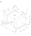
- the multilayer ceramic capacitor 1 is substantially rectangular and includes a capacitor body 1A having a laminate 2 and a pair of external electrodes 3 provided at both ends of the laminate 2, and a spacer 4 attached to the capacitor body 1A.
- the laminate 2 also includes an inner layer 11 in which a dielectric layer 14 and an internal electrode layer 15 are laminated.
- first main surface A1 and the second main surface A2 When it is not necessary to particularly distinguish between the first main surface A1 and the second main surface A2, they will be collectively referred to as a main surface A, when it is not necessary to particularly distinguish between the first side surface B1 and the second side surface B2, they will be collectively referred to as a side surface B, and when it is not necessary to particularly distinguish between the first end surface C1 and the second end surface C2, they will be collectively referred to as an end surface C.
- the laminate 2 preferably has rounded ridges R1, including the corners.
- the ridges R1 are the intersections of two surfaces of the laminate 2, i.e., the main surface A and the side surface B, the main surface A and the end surface C, or the side surface B and the end surface C.
- the inner layer portion 11 includes dielectric layers 14 and internal electrode layers 15 that are alternately stacked along a stacking direction T.
- the dielectric layer 14 is made of a ceramic material, such as a dielectric ceramic containing BaTiO3 as a main component.
- the internal electrode layer 15 includes a plurality of first internal electrode layers 15a and a plurality of second internal electrode layers 15b.
- the first internal electrode layers 15a and the second internal electrode layers 15b are alternately arranged.
- the first internal electrode layer 15a includes a first opposing portion 152a facing the second internal electrode layer 15b, and a first lead portion 151a drawn from the first opposing portion 152a to the first end face C1 side. An end of the first lead portion 151a is exposed to the first end face C1 and is electrically connected to the first external electrode 3a described later.
- the second internal electrode layer 15b includes a second opposing portion 152b facing the first internal electrode layer 15a, and a second lead portion 151b drawn from the second opposing portion 152b to the second end face C2. An end of the second lead portion 151b is electrically connected to the second external electrode 3b described later. Charges are stored in the first opposing portions 152a of the first internal electrode layers 15a and the second opposing portions 152b of the second internal electrode layers 15b.
- the outer layer portion 12 can be formed of the same material as the dielectric layer 14 of the inner layer portion 11 .
- the multilayer ceramic capacitor 1 includes a first side gap portion 16a that is disposed so as to sandwich the inner layer portion 11 and the outer layer portion 12 in the width direction W and that forms a first side surface B1 of the multilayer ceramic capacitor 1, and a second side gap portion 16b that forms a second side surface B2 of the multilayer ceramic capacitor 1.
- the side gap portion 16 can be formed of the same material as the dielectric layer 14.
- the end of the first extension portion 151a of the first internal electrode layer 15a is exposed to the first end face C1 and is electrically connected to the first external electrode 3a.
- the end of the second extension portion 151b of the second internal electrode layer 15b is exposed to the second end face C2 and is electrically connected to the second external electrode 3b.
- the external electrode 3 also includes, for example, a base electrode layer 30 and a first plating layer 31. However, it is not necessarily required that the external electrode 3 has such a layered structure.
- the first plating layer 31 includes a first nickel (Ni) plating layer 31a disposed on the surface of the base electrode layer 30, and a first tin (Sn) plating layer 31b disposed on the surface of the first nickel (Ni) plating layer 31a. Note that the configuration of the first plating layer 31 is not limited to this.
- the spacer 4 includes a pair of a first spacer 4a and a second spacer 4b.
- the first spacer 4a is disposed on one end face C1 side in the length direction L on the second main surface A2 side, which is the substrate mounting surface of the capacitor body 1A
- the second spacer 4b is disposed on the other end face C2 side.
- the substrate mounting surface of the capacitor body 1A is the first side face B1
- the first spacer 4a is disposed on one end face C1 side in the length direction L on the first side face B1 side, which is the substrate mounting surface of the capacitor body 1A
- the second spacer 4b is disposed on the other end face C2 side.
- the spacer 4 is disposed on the external electrode 3 of the capacitor body 1A and on the surface of the second main surface A2 of the laminate 2 on which the subsequent external electrode 3 is not disposed.
- the spacer 4 is disposed on the external electrode 3 of the capacitor body 1A and on the surface of the first side surface B1 of the laminate 2 on which the subsequent external electrode 3 is not disposed.
- the spacer 4 has a substantially rectangular parallelepiped shape, and of the two faces formed on the surface facing the stacking direction T, the face that sandwiches the external electrode 3 between the second main face A2 of the laminate 2 is the first main face SA1, and the face that does not sandwich the external electrode 3 is the second main face SA2.
- the angle of the second main face SA2 of the spacer 4 with respect to the second main face A2 of the laminate 2 is 5 degrees or less when viewed from the width direction W. This allows the multilayer ceramic capacitor 1 to be arranged with the second main face SA2 of the spacer 4 substantially parallel to the wiring board, so that when bonding is performed using solder, no gap is generated between the spacer 4 and the land provided on the wiring board, and bonding can be performed reliably.
- the difference between the amount of solder that enters between the two spacers 4 and the second main face A2 of the laminate 2 can be reduced between the two spacers 4, so that the fluctuation in the relative position of the two spacers 4 caused by the shrinkage of the solder can be suppressed, and the mountability can be improved.
- the substrate mounting surface of the capacitor body 1A is the first side surface B1
- the surface that sandwiches the external electrode 3 between the first side surface B1 of the laminate 2 is defined as the first side surface SB1
- the surface that does not sandwich the external electrode 3 is defined as the second side surface SB2.
- the angle of the second side surface SB2 of the spacer 4 relative to the first side surface B1 of the laminate 2 is 5 degrees or less when viewed from the stacking direction T.
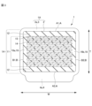
- the spacer 4 is polished perpendicular to the width direction W up to the center of the width direction W, and the polished surface is photographed with a microscope (BX-51) connected to a digital camera for microscopes (DP22, manufactured by Olympus) at a total magnification of 10x.
- a microscope BX-51 connected to a digital camera for microscopes (DP22, manufactured by Olympus) at a total magnification of 10x.
- the angle between a line connecting both ends of the second main surface A2 of the laminate 2 and a line connecting both ends of the second main surface SA2 of the spacer 4 can be measured. If both ends are rounded, the non-rounded parts are regarded as both ends.
- the stretching vibration of the inner layer 11 propagates to the wiring board, which may make it difficult to suppress the occurrence of squeal.
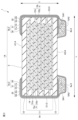
- the spacer 4 is viewed from the width direction W, it is preferable that the length W1 of the length direction L of the first main surface SA1 of the spacer 4 is 95% or less, or 105% or more, of the length W3 of the length direction L of the second main surface SA2 of the spacer 4. This makes it possible to prevent the melted solder from running along the surface of the spacer 4 and wetting up.
- the length W2 of the length direction L of the central portion in the stacking direction T is shorter than the length W1 of the length direction L of the first main surface SA1 and the length W3 of the length direction L of the second main surface SA2.
- the shape can be expressed as W1 ⁇ W2 ⁇ W3 (FIG. 4(b))
- the shape can be expressed as W1>W2>W3 (FIG. 4(c))
- the shape can be expressed as W1>W2 and W2 ⁇ W3 (FIG. 4(d)
- the molten solder can be prevented from running down the surface of the spacer 4 and wetting up.
- the spacer is shaped in this way, the adhesion area with the reinforcing material described later also increases, improving the adhesion force between the spacer and the multilayer ceramic capacitor.
- the substrate mounting surface of the capacitor body 1A is the first side surface B1.
- the spacer 4 is polished perpendicular to the width direction W up to the center of the width direction W, and the polished surface is photographed at a total magnification of 10x using a microscope (BX-51) connected to a digital camera for microscopes (DP22, manufactured by Olympus). The length of each part is measured from the photographed image.
- the second plating layer 32 is disposed so as to cover the spacer 4 and the external electrode 3, but is not limited thereto, and the second plating layer 32 does not have to be disposed on the spacer 4 and the external electrode 3 ( FIG. 9 ).
- the second plating layer 32 includes a second nickel (Ni) plating layer 32a and a second tin (Sn) plating layer 32b disposed on the surface of the second nickel (Ni) plating layer 32a.
- the second plating layer 32 is disposed on the outer surface of the first tin (Sn) plating layer 31b of the first plating layer 31 in the portion where the spacer 4 is not disposed, and is disposed on the outer surface of the spacer 4 in the portion where the spacer 4 is disposed. Note that the configuration of the second plating layer 32 is not limited to this. By disposing the second plating layer 32, the adhesive strength between the spacer 4 and the capacitor body 1A is improved.
- the external electrode 3 is composed of the base electrode layer 30 and the first plating layer 31 covering it, and the spacer 4 is disposed on the surface of the first plating layer 31, but the first plating layer 31 is not necessarily required.
- the spacer 4 may be disposed on the surface of the base electrode layer 30, and the second plating layer 32 may be disposed so as to cover the spacer 4 and the base electrode layer 30.
- the spacer 4 contains either copper (Cu) or nickel (Ni) and tin (Sn) as metal powder.
- the copper (Cu) and nickel (Ni) may be coated with silver (Ag).
- An intermetallic compound formed by adding either copper (Cu) or nickel (Ni) and tin (Sn) can reliably maintain the shape of the spacer 4 without deformation due to heat even when soldering is performed when mounting the multilayer ceramic capacitor 1 on a wiring board.
- an intermetallic compound formed by adding tin (Sn) to an alloy of copper (Cu) and nickel (Ni) is preferable as a component for forming the spacer 4.
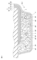
- Phenol resin may be included in the metal region MP formed by the metal powder.
- the phenol resin coats the particles of the intermetallic compound and is scattered so as to fill the gaps between the particles.
- the phenol resin may not completely coat the particles of the intermetallic compound.
- the amount of gas generated during the heat treatment for forming the spacer 4 can be reduced, and therefore the voids P within the spacer 4 can be reduced.
- the phenol resin may be exposed on the surface of the spacer 4 and cover at least a part of the surface of the spacer 4. By coating the surface of the spacer 4 with the phenol resin, the smoothness of the surface of the spacer 4 is improved, and the mechanical strength of the spacer 4 can be increased.
- phenolic resins include novolac-type phenolic resins such as phenol novolac resin, phenol aralkyl resin, cresol novolac resin, tert-butylphenol novolac resin, and nonylphenol novolac resin, resol-type phenolic resin, and polyoxystyrene such as polyparaoxystyrene.
- the area ratio of the phenolic resin in the LT cross section perpendicular to the width direction W of the spacer 4 is preferably 1% to 20%, and more preferably 5% to 15%. If it is less than 1%, the effect of the phenolic resin cannot be fully exerted, and if it exceeds 20%, the adhesive strength of the spacer to the external electrode may decrease.
- the percentage of the area occupied by the phenolic resin can be calculated, for example, by polishing the spacer 4 in the width direction W up to the center of the width direction W, enlarging the polished surface with a microscope (BX-51) at a total magnification of 50 times, and photographing it with a digital camera for microscopes (Olympus DP22).
- metal powder MF may be included in the resin region RP formed by the phenolic resin.
- the metal powder MF can inhibit the shrinkage of the phenolic resin, thereby reducing the shrinkage stress caused by the phenolic resin.
- the spacer 4 preferably has a porosity of 20% or less in the region Z up to 5 ⁇ m from the interface with the external electrode 3. By keeping the porosity low, the bonding area of the spacer 4 that is bonded to the external electrode 3 increases, improving the bonding strength with the external electrode 3.
- the maximum diameter of the void P formed inside the spacer 4 is preferably 1/2 or less of the maximum dimension of the thickness of the spacer 4 in the stacking direction T. If it is greater than 1/2, cracks are more likely to occur starting from the void P, reducing the strength of the spacer 4.
- the maximum diameter of the void P formed inside the spacer 4 is preferably 1/2 or less of the maximum dimension of the thickness of the spacer 4 in the width direction W.
- an example of the material of the spacer 4 is shown to include an intermetallic compound and phenolic resin, but the material is not limited to this and may include other types of metal components, or may include resins such as epoxy resins or rosin, or glass components, other than phenolic resin. It may also be formed without including resin.
- the direction discrimination means indicates the direction so that the second main surface A2 on which the spacer 4 is arranged faces the wiring board when the multilayer ceramic capacitor 1 is mounted on the wiring board, and can be a means for coloring the spacer 4 in a color different from the external electrode 3, a means for printing a mark for discriminating the direction such as a QR code (registered trademark), or a means for providing a recess in a part of the laminate.
- the phenolic resin contained in the spacer 4 may be exposed on the surface of the spacer 4 so that it has a color different from that of the external electrode 3. Even if the spacer 4 is larger than the external electrode 3, a direction discrimination means may be provided.
- a reinforcing material 50 can be arranged between the first spacer 4a and the second spacer 4b so as to cover at least a portion of at least one of the first spacer 4a and the second spacer 4b and at least a portion of the second main surface A2 or the first side surface B1 of the laminate 2.
- the adhesive strength between the spacer 4 and the external electrode 3, and between the spacer 4 and the laminate 2 can be improved.
- the reinforcing material 50 can be arranged continuously between the first spacer 4a and the second spacer 4b, but does not necessarily have to be arranged continuously.
- the reinforcing material 50 may be arranged in two parts: one covering a part of the first spacer 4a and a part of the second main surface A2 or the first side surface B1 of the laminate 2, and the other covering a part of the second spacer 4b and a part of the second main surface A2 or the first side surface B1 of the laminate 2.
- the reinforcing material 50 can be formed from an insulating resin.
- the surface of the insulating resin may be coated with an insulating water-repellent agent.
- the insulating resin may contain ceramics, glass, etc. It may be formed from only the water-repellent agent.
- the material of the reinforcing material 50 is mainly epoxy resin, which can be combined with phenolic resin as a hardener.
- Other hardeners that can be used include acid anhydride-based, amine-based, and ester-based hardeners.
- a hardening accelerator may also be added to the epoxy resin.
- the reinforcing material 50 can be arranged so as to cover the side surface SW of the spacer 4.
- the reinforcing material 50 covers the side surface SW of the spacer 4 to a height of 5% or more of the length of the spacer 4 in the stacking direction T, while covering the second main surface A2 or the first side surface B1 of the laminate 2.
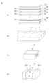
- FIG. 6 is a flow chart for explaining the method for manufacturing the multilayer ceramic capacitor 1.
- the method for manufacturing the multilayer ceramic capacitor 1 includes a laminate manufacturing step S1, a base electrode layer forming step S2, a first plating layer forming step S3, a spacer arranging step S4, and a second plating layer forming step S5.
- the multilayer ceramic capacitor 1 is provided with a reinforcing material 50 by going through a reinforcing material arranging step S6.
- FIG. 7 is a diagram for explaining the laminate manufacturing step S1, the base electrode layer forming step S2, and the first plating layer forming step S3.
- FIG. 8 is a diagram for explaining the spacer arranging step S4 and the second plating layer forming step S5.
- FIG. 11 is a diagram for explaining the reinforcing material arranging step S6.
- a ceramic slurry containing ceramic powder, a binder, and a solvent is formed into a sheet shape on the surface of a carrier film using a die coater, a gravure coater, a microgravure coater, or the like to prepare a laminated ceramic green sheet 101 that will become the dielectric layer 14.
- a conductive paste is printed in stripes on the laminated ceramic green sheet 101 by screen printing, inkjet printing, gravure printing, or the like, and a conductive pattern 102 that will become the internal electrode layer 15 is printed on the surface of the laminated ceramic green sheet 101 to prepare a material sheet 103.
- multiple material sheets 103 are stacked so that the conductive patterns 102 face the same direction and are offset, for example, by half a pitch in the length direction between adjacent material sheets 103. Furthermore, outer layer ceramic green sheets 112 that will become the outer layer 12 are stacked on both sides of the multiple stacked material sheets 103.
- the stacked material sheets 103 and the outer layer ceramic green sheets 112 are pressed together using a hydrostatic press or the like to create the mother block 110 shown in Figure 7(b).
- the mother block 110 is cut along the cutting line X shown in FIG. 7(b) and along the cutting line Y intersecting with the cutting line X to produce a plurality of unsintered laminates 2 shown in FIG. 7(c).
- Base electrode layer formation step S2 Next, a conductive paste containing copper (Cu) is applied to the end faces C of the laminate 2 and baked to form the base electrode layer 30.
- the base electrode layer 30 is formed not only on the end faces C on both sides of the laminate 2 but also on the other end faces C on both sides of the laminate 2.
- the insulating layer 2 is formed so as to extend to the main surface A and the side surface B of the laminate 2 and to cover a part of the end surface C of the main surface A.
- the insulating layer 2 is not limited to this, and may contain other metals and other components.
- two base electrode layers may be provided.
- a first nickel (Ni) plating layer 31a is formed on the surface of the base electrode layer 30, and a first tin (Sn) plating layer 31b is disposed on the surface of the first nickel (Ni) plating layer 31a, thereby producing the capacitor body 1A shown in Figure 7 (d).
- Spacer placement step S4 A spacer manufacturing paste 41 used for manufacturing the spacers is prepared.
- the spacer manufacturing paste 41 contains metals made of copper (Cu), nickel (NI), tin (Sn), and silver (Ag), a phenol resin, a solvent, and an additive.
- phenolic resins include novolac-type phenolic resins such as phenol novolac resin, phenol aralkyl resin, cresol novolac resin, tert-butylphenol novolac resin, and nonylphenol novolac resin, resol-type phenolic resin, and polyoxystyrene such as polyparaoxystyrene.
- a holding substrate 40 as shown in FIG. 8 is used.
- a spacer manufacturing paste 41 is placed on a holding substrate 40 by a screen printing method, a dispense method or the like.
- the capacitor body 1A is mounted on the upper surface of the holding substrate 40 with the second main surface A2 facing the holding substrate 40. At this time, the external electrodes 3 of the capacitor body 1A and the spacer manufacturing paste 41 are aligned, and the spacer manufacturing paste 41 adheres to the capacitor body 1A.
- the heating process is carried out.
- the metal in the paste produces an intermetallic compound and the metal region MP is formed
- some of the phenolic resin is taken into the metal region MP and some is expelled from the metal region MP, while hardening, forming a spacer 4 bonded to the capacitor body 1A.
- the capacitor body 1A is separated from the holding substrate 40 together with the spacer 4, resulting in the state shown in FIG.
- the manufacturing method is not limited to this, and spacers may be formed by applying a spacer manufacturing paste in a desired shape directly on the surface of capacitor body 1A and performing a heat treatment.
- the following method can be used, for example.
- a spacer manufacturing paste is printed on the unfired laminate 2 by screen printing or the like, and then a smooth plate-like jig is pressed against the printed surface. The height of the jig is adjusted to increase the amount of pressure applied to the spacer manufacturing paste, and then heat treatment is performed.
- a spacer manufacturing paste is printed on the unfired laminate 2 by screen printing or the like, and then a smooth plate-like jig is pressed against the printed surface. The height of the jig is adjusted to reduce the amount of pressure applied to the spacer manufacturing paste, and then heat treatment is performed.
- a spacer manufacturing paste is printed on the unsintered laminate 2 by screen printing or the like, and then a smooth, plate-shaped jig is pressed against the spacer manufacturing paste while adjusting its height, and then heat treatment is performed while moving the jig in the direction away from the spacer manufacturing paste so that it does not come off the spacer manufacturing paste.
- an example of the material of the spacer 4 is shown to include an intermetallic compound and phenolic resin, but the material is not limited to this and may include other types of metal components, or may include resins such as epoxy resins or rosin, or glass components, other than phenolic resin. It may also be formed without including resin.
- a second nickel (Ni) plating layer 32a is formed on the exposed portion of the first tin (Sn) plating layer 31b in the capacitor body 1A and on the surface of the spacer 4, and a second tin (Sn) plating layer 32b may be further formed on the outer periphery of the second nickel (Ni) plating layer 32a.
- FIG. 6 is diagrams illustrating the reinforcing material arranging step S6.
- the spacer arranging step S4 the surface of the capacitor body 1A on which the spacers 4 are arranged is cleaned with a solvent. As shown in FIG. After cleaning is completed, the capacitor body 1A with the spacers 4 disposed thereon is aligned so that the spacers 4 face upward.
- a dispenser or squeegee printing is used to form an insulating resin layer that will become the central portion 51 of the reinforcing material 50 between the first spacer 4a and the second spacer 4b on the capacitor body 1A on which the spacer 4 is disposed.
- the amount of insulating resin that wets onto the side surface of the spacer 4 can be adjusted by adjusting the amount of insulating resin.
- the insulating resin can penetrate into the interface between the spacer 4 and the laminate 2, you can do so by suctioning the vacuum after placing the insulating resin.
- the amount of penetration can be controlled by changing the vacuuming time and pressure.
- an insulating resin may be applied so as to cover the outer periphery of the capacitor body 1 A and the outer periphery of the spacer 4 .
- the applied insulating resin is then heated at 100 to 200° C. for 20 to 80 minutes, whereby the insulating resin hardens and forms a covering made of the reinforcing material 50 on the outer periphery of the capacitor body 1A and on the side surface SW of the spacer 4.
- the multilayer ceramic capacitor 1 is manufactured.
- the reinforcing material 50 directly covers the surface of the spacer 4, but this is not necessarily limited to this.
- the second plating layer 32 may be formed on the surface of the spacer 4, and the reinforcing material 50 may be disposed so as to cover the surface of the second plating layer 32 with the side surface SW of the spacer 4.
- the above describes an embodiment of the present invention, but the present invention is not limited to the embodiment, and can be implemented in various forms without departing from the gist of the present invention.
- the present invention includes the following combinations.
- ⁇ 1> a laminate including an inner layer portion in which dielectric layers and internal electrode layers are alternately laminated, the laminate having two main faces opposing each other in a lamination direction, two end faces opposing each other in a length direction intersecting the lamination direction, and two side faces opposing each other in a width direction intersecting the lamination direction and the length direction; Two external electrodes are connected to the internal electrode layers at the two end faces, respectively, and cover the end faces and parts of two opposing main faces.
- a surface sandwiching the external electrode is defined as a first main surface
- a surface not sandwiching the external electrode is defined as a second main surface
- a laminated ceramic electronic component in which an angle of the second main surface of the spacer with respect to the main surface of the laminate on which the spacer is disposed is 5 degrees or less when viewed in the width direction.
- ⁇ 2> The multilayer ceramic electronic component according to ⁇ 1>, wherein, when the spacer is viewed from the width direction, the length of the first main surface in the longitudinal direction is 95% or less, or 105% or more, of the length of the second main surface in the longitudinal direction.
- ⁇ 3> ⁇ 1> or ⁇ 2>, wherein, when the spacer is viewed from the width direction, the length in the longitudinal direction of a central portion in the stacking direction is shorter than the length in the longitudinal direction of the first main surface and the length in the longitudinal direction of the second main surface.
- ⁇ 4> The multilayer ceramic electronic component according to any one of ⁇ 1> to ⁇ 3>, wherein the spacer contains a resin.
- ⁇ 5> The ceramic capacitor according to any one of ⁇ 1> to ⁇ 4>, wherein the spacer contains copper and glass.
- ⁇ 6> The multilayer ceramic capacitor according to any one of ⁇ 1> to ⁇ 5>, wherein the spacer contains a phenol resin.
- ⁇ 7> The multilayer ceramic capacitor according to any one of ⁇ 1> to ⁇ 6>, wherein the spacer contains an epoxy resin.
- ⁇ 8> The multilayer ceramic capacitor according to any one of ⁇ 1> to ⁇ 7>, wherein the spacer contains rosin.
- ⁇ 9> The multilayer ceramic electronic component according to any one of ⁇ 1> to ⁇ 8>, wherein a reinforcing material is disposed between the two spacers, the reinforcing material covering at least a portion of the two spacers and at least a portion of the main surface of the laminate.
- a reinforcing material is disposed between the two spacers, the reinforcing material covering at least a portion of the two spacers and at least a portion of the main surface of the laminate.
- the reinforcing material covers side peripheral surfaces of the two spacers.
- a laminate including an inner layer portion in which dielectric layers and internal electrode layers are alternately laminated, the laminate having two main faces opposing each other in a lamination direction, two end faces opposing each other in a length direction intersecting the lamination direction, and two side faces opposing each other in a width direction intersecting the lamination direction and the length direction;
- Two external electrodes are connected to the internal electrode layers at the two end faces, respectively, and cover the end faces and parts of two side faces adjacent thereto; two spacers disposed on one of the two side surfaces of the laminate with the external electrode therebetween;
- a surface that sandwiches the external electrode is defined as a first side surface
- a surface that does not sandwich the external electrode is defined as a second side surface
- a multilayer ceramic electronic component in which an angle of the second side surface of the spacer with respect to the side surface of the laminate on which the spacer is disposed is 5 degrees or less when viewed from the width direction.
- ⁇ 12> The multilayer ceramic electronic component according to ⁇ 11>, wherein, when the spacer is viewed from the stacking direction, the length of the first side surface in the longitudinal direction is 95% or less, or 105% or more, of the length of the second side surface in the longitudinal direction.
- ⁇ 13> ⁇ 11> or ⁇ 12>, wherein, when the spacer is viewed from the stacking direction, the length in the longitudinal direction of the widthwise center portion is shorter than the length in the longitudinal direction of the first side surface and the length in the longitudinal direction of the second side surface.
- ⁇ 14> The multilayer ceramic electronic component according to any one of ⁇ 11> to ⁇ 13>, wherein the spacer contains a resin.
- ⁇ 15> The ceramic capacitor according to any one of ⁇ 11> to ⁇ 14>, wherein the spacer contains copper and glass.
- ⁇ 16> The multilayer ceramic capacitor according to any one of ⁇ 11> to ⁇ 15>, wherein the spacer contains a phenol resin.
- ⁇ 17> The multilayer ceramic capacitor according to any one of ⁇ 11> to ⁇ 16>, wherein the spacer contains an epoxy resin.
- ⁇ 18> The multilayer ceramic capacitor according to any one of ⁇ 11> to ⁇ 17>, wherein the spacer contains rosin.
- ⁇ 19> The multilayer ceramic electronic component according to any one of ⁇ 11> to ⁇ 18>, wherein a reinforcing material is disposed between the two spacers, the reinforcing material covering at least a portion of the two spacers and at least a portion of the side surface of the laminate.
- a reinforcing material is disposed between the two spacers, the reinforcing material covering at least a portion of the two spacers and at least a portion of the side surface of the laminate.
- the reinforcing material covers side peripheral surfaces of the two spacers.
Landscapes
- Engineering & Computer Science (AREA)
- Power Engineering (AREA)
- Microelectronics & Electronic Packaging (AREA)
- Manufacturing & Machinery (AREA)
- Physics & Mathematics (AREA)
- Electromagnetism (AREA)
- Ceramic Engineering (AREA)
- Chemical & Material Sciences (AREA)
- Inorganic Chemistry (AREA)
- Fixed Capacitors And Capacitor Manufacturing Machines (AREA)
- Ceramic Capacitors (AREA)
Priority Applications (3)
| Application Number | Priority Date | Filing Date | Title |
|---|---|---|---|
| CN202480022048.4A CN120883304A (zh) | 2023-03-30 | 2024-03-18 | 层叠陶瓷电子部件 |
| JP2025510529A JPWO2024203522A1 (https=) | 2023-03-30 | 2024-03-18 | |
| US19/327,189 US20260011504A1 (en) | 2023-03-30 | 2025-09-12 | Multilayer ceramic electronic component |
Applications Claiming Priority (2)
| Application Number | Priority Date | Filing Date | Title |
|---|---|---|---|
| JP2023056330 | 2023-03-30 | ||
| JP2023-056330 | 2023-03-30 |
Related Child Applications (1)
| Application Number | Title | Priority Date | Filing Date |
|---|---|---|---|
| US19/327,189 Continuation US20260011504A1 (en) | 2023-03-30 | 2025-09-12 | Multilayer ceramic electronic component |
Publications (1)
| Publication Number | Publication Date |
|---|---|
| WO2024203522A1 true WO2024203522A1 (ja) | 2024-10-03 |
Family
ID=92904827
Family Applications (1)
| Application Number | Title | Priority Date | Filing Date |
|---|---|---|---|
| PCT/JP2024/010486 Ceased WO2024203522A1 (ja) | 2023-03-30 | 2024-03-18 | 積層セラミック電子部品 |
Country Status (4)
| Country | Link |
|---|---|
| US (1) | US20260011504A1 (https=) |
| JP (1) | JPWO2024203522A1 (https=) |
| CN (1) | CN120883304A (https=) |
| WO (1) | WO2024203522A1 (https=) |
Citations (4)
| Publication number | Priority date | Publication date | Assignee | Title |
|---|---|---|---|---|
| WO2015098990A1 (ja) * | 2013-12-24 | 2015-07-02 | 京セラ株式会社 | 積層型電子部品およびその実装構造体 |
| JP2018207090A (ja) * | 2017-06-08 | 2018-12-27 | サムソン エレクトロ−メカニックス カンパニーリミテッド. | 積層型電子部品及びその実装基板、並びに電子装置 |
| WO2020040138A1 (ja) * | 2018-08-23 | 2020-02-27 | 昭栄化学工業株式会社 | 導電性ペースト |
| JP2022099069A (ja) * | 2020-12-22 | 2022-07-04 | 株式会社村田製作所 | 積層セラミックコンデンサ及び積層セラミックコンデンサの製造方法 |
-
2024
- 2024-03-18 WO PCT/JP2024/010486 patent/WO2024203522A1/ja not_active Ceased
- 2024-03-18 CN CN202480022048.4A patent/CN120883304A/zh active Pending
- 2024-03-18 JP JP2025510529A patent/JPWO2024203522A1/ja active Pending
-
2025
- 2025-09-12 US US19/327,189 patent/US20260011504A1/en active Pending
Patent Citations (4)
| Publication number | Priority date | Publication date | Assignee | Title |
|---|---|---|---|---|
| WO2015098990A1 (ja) * | 2013-12-24 | 2015-07-02 | 京セラ株式会社 | 積層型電子部品およびその実装構造体 |
| JP2018207090A (ja) * | 2017-06-08 | 2018-12-27 | サムソン エレクトロ−メカニックス カンパニーリミテッド. | 積層型電子部品及びその実装基板、並びに電子装置 |
| WO2020040138A1 (ja) * | 2018-08-23 | 2020-02-27 | 昭栄化学工業株式会社 | 導電性ペースト |
| JP2022099069A (ja) * | 2020-12-22 | 2022-07-04 | 株式会社村田製作所 | 積層セラミックコンデンサ及び積層セラミックコンデンサの製造方法 |
Also Published As
| Publication number | Publication date |
|---|---|
| CN120883304A (zh) | 2025-10-31 |
| JPWO2024203522A1 (https=) | 2024-10-03 |
| US20260011504A1 (en) | 2026-01-08 |
Similar Documents
| Publication | Publication Date | Title |
|---|---|---|
| CN114664566B (zh) | 层叠陶瓷电容器以及层叠陶瓷电容器的制造方法 | |
| CN113555215B (zh) | 层叠陶瓷电容器 | |
| JP6696121B2 (ja) | 複合電子部品および抵抗素子 | |
| US20260024699A1 (en) | Multilayer ceramic electronic component | |
| JP7647920B2 (ja) | 積層セラミックコンデンサ及びバンプ製造用ペースト | |
| JP2017022256A (ja) | 複合電子部品および抵抗素子 | |
| CN113539683A (zh) | 层叠陶瓷电容器 | |
| CN113555221A (zh) | 层叠陶瓷电容器 | |
| CN113555220A (zh) | 层叠陶瓷电容器 | |
| US20240258037A1 (en) | Multilayer ceramic capacitor and bump-producing paste | |
| JP7690995B2 (ja) | 積層セラミックコンデンサ及びバンプ製造用ペースト | |
| WO2024203522A1 (ja) | 積層セラミック電子部品 | |
| CN113555219B (zh) | 层叠陶瓷电容器 | |
| CN113555218B (zh) | 层叠陶瓷电容器 | |
| WO2023210465A1 (ja) | 積層セラミックコンデンサ及び積層セラミックコンデンサの実装方法 | |
| WO2024203711A1 (ja) | 積層セラミック電子部品 | |
| US20260011502A1 (en) | Laminated ceramic electronic component | |
| WO2024202402A1 (ja) | 積層セラミック電子部品 | |
| US20260018340A1 (en) | Multilayer ceramic electronic component | |
| KR20250168612A (ko) | 적층 세라믹 전자부품 | |
| WO2025163971A1 (ja) | 積層セラミック電子部品 | |
| WO2025163972A1 (ja) | 積層セラミック電子部品 | |
| WO2025163973A1 (ja) | 積層セラミック電子部品 | |
| WO2025046969A1 (ja) | 積層セラミック電子部品 |
Legal Events
| Date | Code | Title | Description |
|---|---|---|---|
| 121 | Ep: the epo has been informed by wipo that ep was designated in this application |
Ref document number: 24779647 Country of ref document: EP Kind code of ref document: A1 |
|
| ENP | Entry into the national phase |
Ref document number: 2025510529 Country of ref document: JP Kind code of ref document: A |
|
| WWE | Wipo information: entry into national phase |
Ref document number: 2025510529 Country of ref document: JP |
|
| WWE | Wipo information: entry into national phase |
Ref document number: 202480022048.4 Country of ref document: CN |
|
| NENP | Non-entry into the national phase |
Ref country code: DE |
|
| WWP | Wipo information: published in national office |
Ref document number: 202480022048.4 Country of ref document: CN |
|
| 122 | Ep: pct application non-entry in european phase |
Ref document number: 24779647 Country of ref document: EP Kind code of ref document: A1 |