WO2024203308A1 - Baw共振器及び電子機器 - Google Patents
Baw共振器及び電子機器 Download PDFInfo
- Publication number
- WO2024203308A1 WO2024203308A1 PCT/JP2024/009661 JP2024009661W WO2024203308A1 WO 2024203308 A1 WO2024203308 A1 WO 2024203308A1 JP 2024009661 W JP2024009661 W JP 2024009661W WO 2024203308 A1 WO2024203308 A1 WO 2024203308A1
- Authority
- WO
- WIPO (PCT)
- Prior art keywords
- electrode
- layer
- piezoelectric layer
- piezoelectric
- baw resonator
- Prior art date
- Legal status (The legal status is an assumption and is not a legal conclusion. Google has not performed a legal analysis and makes no representation as to the accuracy of the status listed.)
- Ceased
Links
Images

Classifications
-
- H—ELECTRICITY
- H03—ELECTRONIC CIRCUITRY
- H03H—IMPEDANCE NETWORKS, e.g. RESONANT CIRCUITS; RESONATORS
- H03H9/00—Networks comprising electromechanical or electro-acoustic elements; Electromechanical resonators
- H03H9/15—Constructional features of resonators consisting of piezoelectric or electrostrictive material
- H03H9/17—Constructional features of resonators consisting of piezoelectric or electrostrictive material having a single resonator
-
- H—ELECTRICITY
- H10—SEMICONDUCTOR DEVICES; ELECTRIC SOLID-STATE DEVICES NOT OTHERWISE PROVIDED FOR
- H10N—ELECTRIC SOLID-STATE DEVICES NOT OTHERWISE PROVIDED FOR
- H10N30/00—Piezoelectric or electrostrictive devices
- H10N30/01—Manufacture or treatment
- H10N30/07—Forming of piezoelectric or electrostrictive parts or bodies on an electrical element or another base
- H10N30/074—Forming of piezoelectric or electrostrictive parts or bodies on an electrical element or another base by depositing piezoelectric or electrostrictive layers, e.g. aerosol or screen printing
- H10N30/076—Forming of piezoelectric or electrostrictive parts or bodies on an electrical element or another base by depositing piezoelectric or electrostrictive layers, e.g. aerosol or screen printing by vapour phase deposition
-
- H—ELECTRICITY
- H10—SEMICONDUCTOR DEVICES; ELECTRIC SOLID-STATE DEVICES NOT OTHERWISE PROVIDED FOR
- H10N—ELECTRIC SOLID-STATE DEVICES NOT OTHERWISE PROVIDED FOR
- H10N30/00—Piezoelectric or electrostrictive devices
- H10N30/80—Constructional details
- H10N30/85—Piezoelectric or electrostrictive active materials
- H10N30/853—Ceramic compositions
-
- H—ELECTRICITY
- H10—SEMICONDUCTOR DEVICES; ELECTRIC SOLID-STATE DEVICES NOT OTHERWISE PROVIDED FOR
- H10N—ELECTRIC SOLID-STATE DEVICES NOT OTHERWISE PROVIDED FOR
- H10N30/00—Piezoelectric or electrostrictive devices
- H10N30/80—Constructional details
- H10N30/87—Electrodes or interconnections, e.g. leads or terminals
Definitions
- the present invention relates to a BAW resonator and an electronic device.
- BAW resonators have a piezoelectric layer made of a piezoelectric material between two electrode layers. Utilizing the piezoelectric effect of the piezoelectric layer, BAW resonators are used in electronic devices as electronic components such as pressure sensors, acceleration sensors, and AE (acoustic emission) sensors that detect elastic waves, as well as high-frequency filters, piezoelectric actuators, and radio frequency (RF) filters.
- AE acoustic emission
- a BAW resonator for example, a BAW resonator has been disclosed that includes a lower electrode layer including a lower electrode, a piezoelectric layer, and an upper electrode layer, with the piezoelectric layer and the upper electrode layer stacked on top of the lower electrode layer (see, for example, Patent Document 1).
- the piezoelectric layer is laminated between the lower electrode layer and the upper electrode layer with the end faces of the piezoelectric layer exposed, so resonances occurring in the piezoelectric layer tend to occur in an oblique direction rather than in a direction perpendicular to the thickness. Resonances occurring in an oblique direction become transverse waves, which become noise components in the BAW resonator, creating a problem.
- One aspect of the present invention aims to provide a BAW resonator that can suppress the generation of transverse waves from a piezoelectric layer.
- a BAW resonator including a support substrate, an acoustic mirror layer disposed on the support substrate, a first electrode, a piezoelectric layer, and a second electrode, the BAW resonator being formed by stacking the first electrode, the piezoelectric layer, and the second electrode, a resonator region defining layer made of a metal layer spaced apart from the second electrode on a surface of the piezoelectric layer that contacts the second electrode, the first electrode extends outward beyond the piezoelectric layer;
- the resonator region defining layer is provided on a part of the surface of the piezoelectric layer facing the first electrode, on an end face of the piezoelectric layer, and on an exposed portion of the first electrode.
- One aspect of the BAW resonator according to the present invention is capable of suppressing the generation of transverse waves from the piezoelectric layer.
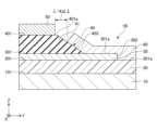
- FIG. 11 is a schematic cross-sectional view showing a configuration of a BAW resonator according to an embodiment of the present invention.
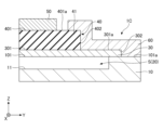
- FIG. 11 is a schematic cross-sectional view showing an example of another configuration of a BAW resonator.
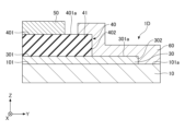
- FIG. 11 is a schematic cross-sectional view showing an example of another configuration of a BAW resonator.
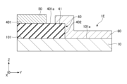
- FIG. 11 is a schematic cross-sectional view showing an example of another configuration of a BAW resonator.
- FIG. 11 is a schematic cross-sectional view showing an example of another configuration of a BAW resonator.
- ⁇ BAW resonator> 1 is a schematic cross-sectional view showing the configuration of a BAW resonator according to this embodiment.
- the BAW resonator 1A includes a support substrate 10, an acoustic mirror layer 20, a first electrode 30, a piezoelectric layer 40, a second electrode 50, and a resonator area defining layer 60.
- the BAW resonator 1A includes a support substrate 10, an acoustic mirror layer 20, a first electrode 30, a piezoelectric layer 40, and a second electrode 50 stacked in this order from the support substrate 10 side.
- the BAW resonator 1A includes a part of the upper surface of the acoustic mirror layer 20, the first electrode 30, and a part of the end of the piezoelectric layer 40 covered with the resonator area defining layer 60.
- the BAW resonator 1A may be formed in any shape, such as a sheet (film).
- a three-dimensional Cartesian coordinate system with three axial directions (X-axis, Y-axis, and Z-axis) is used, with the width direction of the BAW resonator 1A defined as the X-axis direction, the length direction defined as the Y-axis direction, and the height (thickness) direction (vertical direction) defined as the Z-axis direction.
- the second electrode 50 side in the Z-axis direction is defined as the +Z-axis direction, and the supporting substrate 10 side is defined as the -Z-axis direction.
- the +Z-axis direction will be referred to as up or upward
- the -Z-axis direction will be referred to as down or downward, but this does not represent a universal up-down relationship.
- the BAW resonator 1A has a resonator region defining layer 60 that covers a portion of the end of the piezoelectric layer 40 provided on the acoustic mirror layer 20, which prevents the resonance that occurs in the piezoelectric layer 40 from occurring in an oblique direction of the piezoelectric layer 40, thereby preventing transverse waves from being generated from the piezoelectric layer 40 and reducing noise generation.
- the supporting substrate 10 is a substrate on which a laminate of an acoustic mirror layer 20, a first electrode 30, a piezoelectric layer 40, a second electrode 50 and a resonator area defining layer 60 is placed, and may be flexible so as to provide flexibility to the BAW resonator 1A.
- the material forming the support substrate 10 can be any material, regardless of type, as long as it can stably support the laminate.
- a plastic substrate, metal foil, metal plate, silicon (Si) substrate, inorganic dielectric substrate, glass substrate, etc. may be used.
- Plastic substrate Materials that can be used to form the plastic substrate include, for example, polyethylene terephthalate (PET), polyethylene naphthalate (PEN), polycarbonate (PC), acrylic resins, cycloolefin polymers, polyamide (PA) resins, polyimide (PI) resins, polyphenylene sulfide (PPS), polytetrafluoroethylene (PTFE), diallyl phthalate resin (PDAP), etc.
- PET polyethylene terephthalate
- PEN polyethylene naphthalate
- PC polycarbonate
- acrylic resins cycloolefin polymers
- PA polyamide
- PI polyimide
- PPS polyphenylene sulfide
- PTFE polytetrafluoroethylene
- PDAP diallyl phthalate resin
- Materials that can be used to form the metal foil include metals such as Au, Pt, Ag, Ti, Al, Mo, Ru, and Cu.
- Materials that can be used to form the metal plate include, for example, aluminum, copper, stainless steel, tantalum, etc.
- Materials for forming the inorganic dielectric substrate may include, for example, MgO, sapphire, etc.
- the thickness of the support substrate 10 is not particularly limited and may be appropriately determined depending on the application of the BAW resonator 1A, the material of the support substrate 10, etc., and may be, for example, 20 ⁇ m to 725 ⁇ m. If the thickness of the support substrate 10 is 20 ⁇ m to 725 ⁇ m, it can stably support the laminate including the laminate of the acoustic mirror layer 20, the first electrode 30, the piezoelectric layer 40, and the second electrode 50. Furthermore, warping of the support substrate 10 is suppressed and the effect of the warping of the support substrate 10 on the piezoelectric characteristics can be reduced, so that the BAW resonator 1A can have the desired flexibility.
- the thickness of the supporting substrate 10 refers to the length in the direction perpendicular to the main surface of the supporting substrate 10. There are no particular limitations on the method for measuring the thickness of the supporting substrate 10, and any measuring method can be used.
- the thickness of the supporting substrate 10 may be, for example, the thickness measured at any location on the cross section of the supporting substrate 10, or it may be measured at several locations and the average value of these measured values.
- the definition of thickness is the same for other members.
- the acoustic mirror layer 20 is provided on the upper main surface (top surface) 101 of the support substrate 10.
- the acoustic mirror layer 20 may be composed of an acoustic multilayer film having different specific acoustic impedances.
- the acoustic mirror layer 20 is a multilayer film in which two or more pairs of a high acoustic impedance layer having a predetermined specific acoustic impedance and a low acoustic impedance layer having a lower specific acoustic impedance than the high acoustic impedance layer are alternately laminated.
- the vibration energy of the resonance is reflected by the acoustic mirror layer 20.
- the speed at which the vibration wave (elastic wave) propagates through the high acoustic impedance layer is different from the speed at which it propagates through the low acoustic impedance layer.
- the high acoustic impedance layer is made of a material having a high density or bulk modulus, such as W, Mo, Ta 2 O 5 , ZnO, etc.
- the low acoustic impedance layer is made of a material having a lower density or bulk modulus than the high acoustic impedance layer.
- the low acoustic impedance layer is formed of a material having a low density or deposition modulus, such as SiO2 .
- the low acoustic impedance layer may be an amorphous layer or a layer in which the amorphous phase is predominant.
- the high acoustic impedance layer and the low acoustic impedance layer may be formed on the support substrate 10 by sputtering or the like.
- the first electrode 30 is provided on the main surface (top surface) 201 above the acoustic mirror layer 20.
- the first electrode 30 may be formed in the form of a thin film on a part of or the entire top surface 201 of the acoustic mirror layer 20.
- the first electrode 30 is provided so as to extend outward beyond the piezoelectric layer 40. Note that the first electrode 30 extending outward beyond the piezoelectric layer 40 refers to a state in which the first electrode 30 is also disposed outside the piezoelectric layer 40 in a plan view seen from the stacking direction of the first electrode 30.
- the first electrode 30 can be made of any conductive material.
- the material include metals such as Pt, Au, Ag, Cu, Mg, Al, Si, Ti, Cr, Fe, Ni, Zn, Rb, Zr, Nb, Mo, Rh, Pd, Ru, Sn, Ir, Ta, and W.
- the first electrode 30 may be an amorphous film.
- an amorphous film it is possible to suppress unevenness on the surface of the first electrode 30 and the generation of grain boundaries that cause leak paths.
- the thickness of the first electrode 30 can be designed as appropriate, and may be, for example, 40 nm to 300 nm. If the thickness of the first electrode 30 is 40 nm to 300 nm, the first electrode 30 can function as an electrode, and the BAW resonator 1A can be made thin.
- the piezoelectric layer 40 is provided on a main surface (upper surface) 301 above the first electrode 30.
- An end face of the piezoelectric layer 40 may be provided substantially perpendicular to the upper surface 301 of the first electrode 30. In other words, an angle between an end face 402 of the piezoelectric layer 40 and a plane parallel to the upper surface 301 of the first electrode 30 may be approximately 90°.
- the piezoelectric layer 40 preferably contains an inorganic material as a main component.
- the main component means that the content of the inorganic material is 95 atm% or more, preferably 98 atm% or more, and more preferably 99 atm% or more.
- piezoelectric materials having a perovskite crystal structure (perovskite crystal material) and piezoelectric materials having a wurtzite crystal structure (wurtzite crystal material) can be used.
- the wurtzite crystal structure has the general formula AB, where A is an electropositive element and B is an electronegative element.
- Wurtzite crystal materials have a hexagonal unit cell with the polarization vector parallel to the c-axis.
- the wurtzite crystal material it is preferable to use a material that exhibits piezoelectric characteristics of a certain value or more and can be crystallized in a low-temperature process of 200°C or less.
- the wurtzite crystal material contains Zn, Al, Ga, Cd, Si, etc. as the positive element A represented by the general formula AB.
- the wurtzite crystal material for example, zinc oxide (ZnO), zinc sulfide (ZnS), zinc selenide (ZnSe), zinc telluride (ZnTe), aluminum nitride (AlN), gallium nitride (GaN), cadmium selenide (CdSe), cadmium telluride (CdTe), silicon carbide (SiC), etc.
- ZnO is preferable as the wurtzite crystal material because it is relatively easy to orient the c-axis even in a low-temperature process.
- ZnO is preferable as the wurtzite crystal material because it is relatively easy to orient the c-axis even in a low-temperature process.
- ZnO is preferable as the wurtzite crystal material because it is relatively easy to orient the c-axis even in a low-temperature process.
- these may be used alone or in combination of two or more types. When two or
- the wurtzite crystal material preferably contains ZnO, more preferably consists essentially of ZnO, and even more preferably consists only of ZnO. "Substantially” means that in addition to ZnO, it may contain unavoidable impurities that may be inevitably contained during the manufacturing process.
- Inorganic materials such as wurtzite crystal materials may contain, in addition to the above-mentioned ZnO, AlN, ZnS, ZnSe, and ZnTe, alkaline earth metals such as Mg, Ca, and Sr, or metals such as V, Ti, Zr, Si, Sr, and Li, in a predetermined range of proportions. These components may be contained in the elemental state or in the oxide state.
- Mg-doped ZnO in which ZnO is doped with Mg, is preferred as the inorganic material, as it achieves both the K value, which is an index of the piezoelectric properties of the piezoelectric layer 40, and the Q value, which is an index of the steepness of the piezoelectric properties, and exhibits excellent piezoelectric properties.
- the K value is the value of the electromechanical coupling constant k.
- the square value ( k2 value) of the electromechanical coupling constant k of the piezoelectric material contained in the piezoelectric layer 40 indicates the energy conversion efficiency of the electrical energy determined for the piezoelectric material.
- the higher the energy conversion efficiency of the electrical energy the better the operation efficiency of the BAW resonator 1A including the piezoelectric layer 40, and the BAW resonator 1A has excellent piezoelectric characteristics.
- the smaller the disturbance of the crystal orientation of the piezoelectric material contained in the piezoelectric layer 40 the larger the k2 value of the piezoelectric material becomes while gradually becoming constant.
- the Q value is a value that indicates the sharpness (peakedness) of frequency characteristics. The higher the Q value, the sharper the frequency characteristics will be.
- the amount of the additive element in the piezoelectric layer 40 is not particularly limited, and may be within a range that allows the piezoelectric layer 40 to have a wurtzite crystal structure.
- the method for measuring the amount of the additive element contained in the piezoelectric layer 40 is not particularly limited, as long as it is a measurable method.
- the amount of the additive element contained in the piezoelectric layer 40 may be measured, for example, by Rutherford backscattering spectrometry (RBS) using a Pelletron 3SDH (manufactured by NEC Corporation) as a measuring device, or may be measured by secondary ion mass spectrometry using a dynamic SIMS (D-SIMS) or the like.
- RBS Rutherford backscattering spectrometry
- Pelletron 3SDH manufactured by NEC Corporation
- D-SIMS dynamic SIMS
- the thickness of the piezoelectric layer 40 is not particularly limited, and it is sufficient that it has sufficient piezoelectric properties, i.e., polarization properties proportional to pressure, and that it is possible to reduce the occurrence of cracks in the piezoelectric layer 40 and stably exhibit the piezoelectric properties.
- the thickness of the piezoelectric layer 40 may be, for example, 50 nm to 5 ⁇ m. If the thickness of the piezoelectric layer 40 is 50 nm to 5 ⁇ m, the occurrence of cracks is suppressed and sufficient piezoelectric properties can be exhibited.
- the crystal orientation of the piezoelectric layer 40 is preferably 5° or less. If the crystal orientation is 5° or less, the crystal orientation in the c-axis direction (c-axis orientation) of the piezoelectric material contained in the piezoelectric layer 40 is good, and the energy conversion efficiency is improved, thereby improving the piezoelectric characteristics in the thickness direction of the piezoelectric layer 23. If the piezoelectric layer 40 contains ZnO as the piezoelectric material, ZnO has a wurtzite crystal structure, and there is a higher correlation between the crystal orientation and the piezoelectric characteristics than with piezoelectric materials having other crystal structures. If the crystal orientation of ZnO is 5° or less, it is easier to increase the energy conversion efficiency, and the piezoelectric characteristics of the BAW resonator 1A can be improved.
- the crystal orientation of the piezoelectric layer 40 can be evaluated by the full width at half maximum (FWHM) obtained when the surface of the piezoelectric layer 40 is measured by the X-ray rocking curve (XRC) method.
- FWHM full width at half maximum
- XRC X-ray rocking curve
- the FWHM indicates the degree of parallelism of the arrangement of the crystals constituting the piezoelectric material in the c-axis direction. Therefore, the FWHM of the peak waveform of the rocking curve obtained by the XRC method can be used as an indicator of the c-axis orientation of the piezoelectric layer 40. Therefore, the smaller the FWHM of the rocking curve, the better the crystal orientation of the piezoelectric layer 40 in the c-axis direction.
- the crystal orientation of the piezoelectric layer 40 may be evaluated using the XRC method to measure diffraction from a specific crystal plane of the piezoelectric material in the piezoelectric layer 40 (e.g., the (0002) plane of a ZnO crystal) and the FWHM of the rocking curve obtained, as well as the peak intensity. That is, the crystal orientation of the piezoelectric layer 40 may be evaluated using the value obtained by dividing the integrated value of the peak intensity by the FWHM as the evaluation value. For example, the larger the evaluation value obtained by dividing the integrated value of the peak intensity by the FWHM, the better the crystal orientation of the piezoelectric layer 40 can be evaluated to be.
- the piezoelectric layer 40 may be constructed by laminating piezoelectric layers made of each inorganic material.
- the second electrode 50 is provided on the upper principal surface (top surface) 401 of the piezoelectric layer 40, and is disposed so as to face the first electrode 30.
- the second electrode 50 can be formed of any material having electrical conductivity, and the same material as the first electrode 30 can be used.
- the second electrode 50 may be formed as a thin film on a part of or the entire upper surface 401 of the piezoelectric layer 40, or may be formed in any suitable shape.
- the thickness of the second electrode 50 can be designed as appropriate, and is preferably, for example, 40 nm to 300 nm. If the thickness of the second electrode 50 is within the above preferred range, it can function as an electrode and the BAW resonator 1A can be made thin.
- the resonator region defining layer 60 is formed so as to cover a part of the upper surface 201 of the acoustic mirror layer 20, the first electrode 30, and a part of the end portion 41 of the piezoelectric layer 40.
- the resonator region defining layer 60 is provided around the entire periphery of the acoustic mirror layer 20, the first electrode 30, and the piezoelectric layer 40.
- the resonator region defining layer 60 is an exposed portion 201 a of the upper surface 201 of the layer 20, an exposed portion 301 a and an end surface 302 of the upper surface 301 of the first electrode 30, and an exposed portion 401 a and an end surface 402 of the upper surface 401 of the piezoelectric layer 40. It is provided.
- the upper surfaces of the acoustic mirror layer 20, the first electrode 30, and the piezoelectric layer 40 are the surfaces of these layers facing the second electrode 50, and are the main surfaces of these layers that come into contact with the layers stacked on top of them.
- the upper surface 401 of the piezoelectric layer 40 is the main surface that comes into contact with the second electrode 50.
- the lower surfaces of the acoustic mirror layer 20, the first electrode 30, and the piezoelectric layer 40 are the surfaces on which each of these layers faces the support substrate 10, and are the main surfaces on which each of these layers comes into contact with the layer on which it is mounted.
- the bottom surfaces of the acoustic mirror layer 20, the first electrode 30, and the piezoelectric layer 40 are different from the top and bottom surfaces of each of these layers.
- the upper and lower surfaces of the acoustic mirror layer 20, the first electrode 30, and the piezoelectric layer 40 may or may not have the same area.
- the end surface may have a forward tapered shape with an obtuse angle formed with the upper surface.
- the resonator region defining layer 60 has the function of suppressing resonance occurring in the piezoelectric layer 40 from occurring in the thickness direction and diagonal directions.
- the material forming the resonator region defining layer 60 may be any material that can have the same potential as the first electrode 30, and examples of the material that can be used to form the resonator region defining layer 60 include Au, Ag, Al, and Cu. These may be used alone or in combination of two or more of these. Since the resonator region defining layer 60 also shares wiring, it is preferable that the material forming the resonator region defining layer 60 be a metal with high conductivity such as Au, Ag, Al, and Cu.
- the resonator region defining layer 60 may be formed using commonly used methods such as vapor deposition and coating.
- the thickness of the resonator region defining layer 60 should be sufficient to cover the ends of the piezoelectric layer 40, and is preferably 50 nm or more, more preferably 100 nm or more, and even more preferably 200 nm or more. If the thickness of the resonator region defining layer 60 is 50 nm or more, it is possible to suppress resonance occurring in the piezoelectric layer 40 from occurring in a direction oblique to the thickness.
- the thickness of the resonator region defining layer 60 may be the same or different from the top surface 401 of the piezoelectric layer 40 to the acoustic mirror layer 20, but it is preferable that the thickness of the resonator region defining layer 60 located on the end surface 402 of the piezoelectric layer 40 is thicker than the thickness of the resonator region defining layer 60 provided on the top surface 401 of the piezoelectric layer 40.
- the manufacturing method of the BAW resonator 1A is not particularly limited, and any suitable manufacturing method can be used. An example of a manufacturing method of the BAW resonator 1A will be described below.
- high acoustic impedance layers and low acoustic impedance layers are stacked alternately on the upper surface of a support substrate 10 formed to a predetermined size, forming an acoustic mirror layer 20 by stacking high acoustic impedance layers and low acoustic impedance layers in pairs.
- the method for forming the high acoustic impedance layer and the low acoustic impedance layer is not particularly limited, and may be either a dry process or a wet process. If a dry process is used as the method for forming the high acoustic impedance layer and the low acoustic impedance layer, thin high acoustic impedance layer and low acoustic impedance layer can be easily formed.
- Examples of dry processes include sputtering and vapor deposition, while examples of wet processes include plating.
- DC direct current
- RF radio frequency magnetron sputtering
- sputtering is preferred as a method for forming the high acoustic impedance layer and the low acoustic impedance layer.
- the high acoustic impedance layer may be, for example, a thin film formed by a material with high density or bulk modulus, such as W, Mo, Ta 2 O 5 , or ZnO, deposited by DC or RF magnetron sputtering.
- a material with high density or bulk modulus such as W, Mo, Ta 2 O 5 , or ZnO, deposited by DC or RF magnetron sputtering.
- the low acoustic impedance layer may be an oxide film such as a SiO 2 film formed by DC or RF magnetron sputtering.
- sputtering may be performed using a metal or a metal oxide.
- the high acoustic impedance layer is a ZnO film formed by DC or RF magnetron sputtering
- sputtering may be performed using a Zn sputtering target or a ZnO sputtering target depending on the gas atmosphere.
- the first electrode 30 is deposited (formed) on the upper surface of the acoustic mirror layer 20.
- the method for forming the first electrode 30 is not particularly limited, and either a dry process or a wet process may be used, similar to the method for forming the high acoustic impedance layer and the low acoustic impedance layer. Details of the dry process and the wet process are similar to the method for forming the high acoustic impedance layer and the low acoustic impedance layer, so they will not be described here.
- the first electrode 30 may be formed on the entire upper surface 201 of the acoustic mirror layer 20.
- the first electrode 30 may also be formed into any shape by processing the first electrode 30 into a pattern having a predetermined shape by etching or the like.
- the piezoelectric layer 40 is formed on the upper surface 301 of the first electrode 30.
- the piezoelectric layer 40 may be formed by DC or RF magnetron sputtering in a mixed gas atmosphere containing an inert gas such as Ar and a trace amount of oxygen, using a target containing the elements that make up the piezoelectric material.
- the piezoelectric layer 40 is formed by sputtering the piezoelectric material onto the first electrode 30.
- the laminate consisting of the support substrate 10, the acoustic mirror layer 20, and the first electrode 30 may be placed on a deposition plate, which serves as an anode, in a deposition chamber of a sputtering device.
- the deposition plate may be rotatable, for example.
- the laminate consisting of the support substrate 10, the acoustic mirror layer 20, and the first electrode 30 may be wound around a drum roll, which is a film-forming roll, instead of a film-forming plate, as an anode.
- a drum roll By placing a drum roll in a film-forming chamber, the piezoelectric layer 40 can be continuously formed on the first electrode 30 while the laminate consisting of the support substrate 10, the acoustic mirror layer 20, and the first electrode 30 is transported by a roll-to-roll method.
- a target containing the elements that make up the piezoelectric material is used as the cathode.
- a target containing a wurtzite crystal material may be used.
- a target containing a wurtzite crystal material multiple or single targets containing the wurtzite crystal material contained as a main component in the piezoelectric layer 40 may be used.
- the multiple or single targets may be arranged to face the deposition plate at a distance.
- a multi-target sputtering method is used when multiple targets are used as cathodes, and a one-dimensional sputtering method is used when a single target is used as a cathode, to form the piezoelectric layer 40 containing a wurtzite crystal material.
- each target contains a different type of material that constitutes the wurtzite crystal material contained as the main component in the piezoelectric layer 40.
- a target containing Zn, a target containing Si or Sn, and a target containing Al or Mg may be used.
- Each target may be a metal oxide target containing oxygen.
- the multiple targets may be placed in the deposition chamber at intervals. During sputtering, the power applied to each target is adjusted according to the type of wurtzite crystal material contained in the piezoelectric layer 40, and the atomic ratio between each material that constitutes the piezoelectric layer 40 is adjusted.
- the single target When a single target is used as the cathode, the single target contains the wurtzite crystal material contained in the piezoelectric layer 40.
- an alloy target in which the atomic ratio of the wurtzite crystal material contained in the piezoelectric layer 40 is adjusted may be used.
- an alloy target containing Zn, Si or Sn, and Al or Mg may be used.
- the alloy target may be a metal oxide target containing a wurtzite crystal material and oxygen.
- a ZnO sintered compact target may be used as the target.
- a ZnO sintered compact target is placed in a sputtering device, and a mixed gas containing an inert gas such as Ar and oxygen is supplied into the sputtering device.
- a piezoelectric layer 40 can be obtained on the first electrode 30 while suppressing the amount of inert gas that gets in during the deposition of the ZnO film.
- the piezoelectric material is, for example, a wurtzite crystal material made of MgZnO containing ZnO and MgO in a predetermined mass ratio
- a multi-source sputtering method may be used using a target made of ZnO sintered body and a target made of MgO sintered body.
- a one-dimensional sputtering method may be used using an alloy target containing ZnO and MgO, such as a target made of ZnO sintered body to which MgO has been added in advance at a predetermined ratio.
- a multi-target sputtering device is used as the sputtering device, and a mixed gas containing an inert gas such as Ar and oxygen is supplied into the multi-target sputtering device.
- a mixed gas containing an inert gas such as Ar and oxygen
- a ZnO sintered compact target and an MgO sintered compact target are simultaneously and independently sputtered onto the first electrode 30, thereby forming a piezoelectric layer 40 composed of a MgZnO thin film on the first electrode 30.
- a sputtering device When using the one-dimensional sputtering method, a sputtering device is used to perform sputtering in a mixed gas atmosphere containing an inert gas such as Ar and oxygen, using, for example, a target of ZnO sintered body to which MgO has been added in advance at a predetermined ratio, thereby forming a piezoelectric layer 40 composed of a thin MgZnO film on the first electrode 30.
- the gas atmosphere during sputtering may be an inert gas atmosphere or a mixed gas atmosphere containing an inert gas and oxygen.
- the pressure in the gas atmosphere during sputtering may be determined appropriately depending on the type of piezoelectric material, the sputtering method, etc., and may be, for example, 0.1 Pa to 2.0 Pa.
- the deposition temperature of the piezoelectric layer 40 is not particularly limited and may be appropriately selected depending on the layer structure of the BAW resonator 1A, for example, the piezoelectric layer 40 may be deposited at 150°C or lower.
- the sputtering method to deposit the first electrode 30 and the piezoelectric layer 40, it is possible to form a uniform film with strong adhesion while maintaining the composition ratio of the compound target. In addition, by simply controlling the time, it is possible to precisely form the first electrode 30 and the piezoelectric layer 40 to the desired thickness.
- the piezoelectric layer 40 may be constructed by laminating multiple layers.
- the end surface 402 of the piezoelectric layer 40 may be processed so that the angle between the end surface 402 of the piezoelectric layer 40 and a plane parallel to the upper surface 301 of the first electrode 30 is approximately 90°.
- a general method such as dry etching using a reactive gas such as Cl 2 , CF 4 , or CHF 3 , or wet etching using an acidic solution such as HCl or HNO 3 can be used.
- the resonator region defining layer 60 is formed on the upper surface 401 and end surface 402 of the piezoelectric layer 40.
- the resonator region defining layer 60 may be formed using a method similar to that used to form the first electrode 30 on the upper surface 201 of the acoustic mirror layer 20.
- a second electrode 50 having a predetermined shape is formed on the upper surface of the piezoelectric layer 40.
- the second electrode 50 can be formed using the same method as the first electrode 30.
- the thickness of the second electrode 50 can be designed as appropriate and may be, for example, 40 nm to 300 nm.
- the second electrode 50 may be formed on a portion of the upper surface 401 of the piezoelectric layer 40, or may be formed in any suitable shape.
- a resonator region defining layer 60 is formed on the upper surfaces of the acoustic mirror layer 20 and the first electrode 30, and on the ends of the piezoelectric layer 40 (upper surface 401 and end surface 403 of the piezoelectric layer 40).
- a dry process or a wet process may be used, similar to the method for forming the high acoustic impedance layer and the low acoustic impedance layer. Details of the dry process and the wet process are similar to the method for forming the high acoustic impedance layer and the low acoustic impedance layer, so they will not be described here.
- the BAW resonator 1A is formed by forming a second electrode 50 on the upper surfaces of the acoustic mirror layer 20 and the first electrode 30, and on the end of the piezoelectric layer 40.
- the entire BAW resonator 1A may be heat-treated. This heat treatment can crystallize the first electrode 30 and the second electrode 50, lowering their resistance. Heat treatment is not essential, and may not be performed after the formation of the BAW resonator 1A in cases such as when the support substrate 10 is made of a material that is not heat-resistant.
- the BAW resonator 1A comprises a support substrate 10, a first electrode 30, a piezoelectric layer 40, a second electrode 50, and a resonator area defining layer 60.
- the first electrode 30 extends outward beyond the piezoelectric layer 40
- the resonator area defining layer 60 is made of a metal layer and is spaced apart from the second electrode 50 on the upper surface 401 of the piezoelectric layer 40, and is provided on a part of the upper surface 401 and the end surface 402 of the piezoelectric layer 40.
- the end 41 of the piezoelectric layer 40 is covered with the resonator region defining layer 60, so that when vibration occurs in the piezoelectric layer 40, the vibration of the end 41 can be suppressed by the resonator region defining layer 60. Therefore, the BAW resonator 1A can suppress the generation of transverse waves at the end of the piezoelectric layer 40.
- the BAW resonator 1A can suppress the generation of noise caused by transverse waves by suppressing the generation of transverse waves at the end 41 of the piezoelectric layer 40.
- the BAW resonator 1A can have the resonator region defining layer 60 provided continuously from the end face 402 of the piezoelectric layer 40 to the exposed portion of the first electrode.
- the BAW resonator 1A can more reliably cover the end 41 of the piezoelectric layer 40 and more reliably suppress vibration of the end 41 of the piezoelectric layer 40, thereby more reliably suppressing the generation of transverse waves at the end 41 of the piezoelectric layer 40.
- the BAW resonator 1A can provide the resonator area defining layer 60 on the top surface 301 and end surface 302 as exposed portions of the first electrode 30.
- the BAW resonator 1A can more reliably cover the end 41 of the piezoelectric layer 40 and more reliably suppress vibration of the end 41 of the piezoelectric layer 40, thereby more reliably suppressing the generation of transverse waves at the end 41 of the piezoelectric layer 40.
- the BAW resonator 1A may include at least one of Al, Cu, and Au in the resonator region defining layer 60. Since Al, Cu, and Au are easily made to have the same potential as the first electrode 30 and have high conductivity, the BAW resonator 1A can use the resonator region defining layer 60 as wiring while suppressing vibrations generated at the end 41 of the piezoelectric layer 40 with the resonator region defining layer 60.
- the angle between the end face 402 of the piezoelectric layer 40 and a plane parallel to the upper surface 301 of the first electrode 30 can be approximately 90°.
- the end face 41 of the piezoelectric layer 40 is approximately perpendicular to the upper surface 301 of the first electrode 30, it can be covered with the resonator area defining layer 60, so that when vibration occurs in the piezoelectric layer 40, the vibration of the end face 41 can be suppressed by the resonator area defining layer 60.
- the BAW resonator 1A can have a resonator region defining layer 60 with a thickness of 50 nm or more. This allows the resonator region defining layer 60 to suppress vibrations at the end 41 of the piezoelectric layer 40 and suppress the generation of transverse waves. Therefore, even when used for a long period of time, the BAW resonator 1A can suppress deterioration of the piezoelectric properties of the piezoelectric layer 40 and reliably maintain the piezoelectric properties.
- the first electrode 30 and the second electrode 50 of the BAW resonator 1A can be configured to include at least one of Pt, W, Mo, Ru, and Ir.
- the BAW resonator 1A can include MgZnO in the piezoelectric layer 40 as a piezoelectric material.
- MgZnO in the piezoelectric layer 40 as a piezoelectric material.
- the K value and the Q value of a piezoelectric layer formed by doping a piezoelectric material with other elements there is a trade-off between the K value and the Q value of a piezoelectric layer formed by doping a piezoelectric material with other elements, and when a piezoelectric element is used in a high-frequency filter that extracts only signals in a high-frequency range such as the 5 GHz band and removes signals in other frequency bands, the Q value tends to decrease when the required K value is obtained in the high-frequency range.
- the BAW resonator 1A can stably exhibit piezoelectric characteristics even in the high-frequency range of a high-frequency filter, etc.
- the BAW resonator 1A can effectively be used as a BAW filter because it reduces noise generation and has excellent piezoelectric properties, even in high frequency bands.
- the BAW resonator 1A can reduce noise generation and have excellent piezoelectric characteristics, it can also be used in electronic devices for various purposes as an electronic component that utilizes the positive piezoelectric effect or the inverse piezoelectric effect in electronic devices, in addition to BAW filters.
- the BAW resonator 1A is not limited to the above configuration, and other configurations may be used as long as the end 41 of the piezoelectric layer 40 is covered with the resonator region defining layer 60 to suppress the generation of transverse waves from the piezoelectric layer 40.
- An example of another configuration of the BAW resonator 1A is shown below.
- the BAW resonator 1B may be provided with the piezoelectric layer 40 so that its end face 402 is inclined.
- the angle between the end face 402 of the piezoelectric layer 40 and a plane parallel to the upper surface 301 of the first electrode 30 may be less than 90°. This prevents deterioration of the film quality on the surface of the end face 402 of the piezoelectric layer 40 and in the depth direction near it.
- the BAW resonator 1B can cover the end face 402 of the piezoelectric layer 40 with the resonator region defining layer 60 while preventing deterioration from the end of the piezoelectric layer 40, thereby preventing the generation of transverse waves from the end 41 of the piezoelectric layer 40 and preventing deterioration of the piezoelectric characteristics.
- the BAW resonator 1B has the resonator region defining layer 60 located at a position that is spaced apart from the second electrode 50 in the width direction by ⁇ /4 or more, where ⁇ is the wavelength of the resonant frequency defined by the thickness of the piezoelectric layer 40.
- ⁇ is the wavelength of the resonant frequency defined by the thickness of the piezoelectric layer 40.
- the BAW resonator 1B can further suppress the generation of transverse waves while suppressing the deterioration of the piezoelectric characteristics.
- the BAW resonator 1A has an acoustic mirror layer 20 formed of an acoustic multilayer film, but the acoustic mirror layer 20 may also be formed of a space.
- the BAW resonator 1C may have a recess 11 on the upper surface 101 of the support substrate 10, and the space S formed between the recess 11 of the support substrate 10 and the first electrode 30 may function as the acoustic mirror layer 20.
- the resonator region defining layer 60 may be provided on the exposed portion 101a of the upper surface 101 of the support substrate 10, the exposed portion 101a and end surface 302 of the upper surface 301 of the first electrode 30, and the exposed portion 401a and end surface 402 of the upper surface 401 of the piezoelectric layer 40.
- the support substrate 10 may be a conductive substrate.
- the support substrate 10 can also function as the first electrode, so the BAW resonator 1A does not need to include the first electrode 30.
- the BAW resonator 1E may include the support substrate 10, the piezoelectric layer 40, and the second electrode 50, which are stacked in this order from the support substrate 10 side.
- the support substrate 10 may be a metal plate, or may be a conductive transparent substrate such as ITO, IZO, IZTO, or IGZO.
- the support substrate 10 is a metal plate
- a metal film such as Al foil, Cu foil, Al-Ti alloy foil, Cu-Ti alloy foil, or stainless steel foil may be used.
- the thickness of the metal film is thin, the flexibility of the support substrate 10 is high, so a metal adhesive film such as Ti or Ni may be inserted between the support substrate 10 and the piezoelectric layer 40.
- the thickness of the BAW resonator 1E can be reduced by the thickness of the first electrode 30. This allows the overall thickness of the BAW resonator 1F to be reduced, making it possible to reduce the size.
- a first electrode, a piezoelectric layer, and a second electrode are laminated in this order on a supporting substrate, a resonator region defining layer made of a metal layer is provided on a surface of the piezoelectric layer that is in contact with the second electrode and is spaced apart from the second electrode; the first electrode extends outward beyond the piezoelectric layer,
- the BAW resonator has a resonator region defining layer provided on a part of a surface of the piezoelectric layer facing the second electrode and on an end surface of the piezoelectric layer.
- ⁇ 2> The BAW resonator according to ⁇ 1>, wherein the resonator region defining layer is provided continuously from an end face of the piezoelectric layer to an exposed portion of the first electrode.
- ⁇ 3> The BAW resonator according to ⁇ 2>, wherein the exposed portion of the first electrode is an end face of the first electrode and at least a part of a surface of the first electrode facing the piezoelectric layer.
- ⁇ 5> The BAW resonator according to any one of ⁇ 1> to ⁇ 4>, wherein the resonator region defining layer contains at least one of Al, Cu, and Au.
- ⁇ 6> The BAW resonator according to any one of ⁇ 1> to ⁇ 5>, wherein the resonator region defining layer is spaced from the second electrode in a width direction by ⁇ /4 or more, where ⁇ is a wavelength of a resonant frequency defined by a thickness of the piezoelectric layer.
- ⁇ 7> The BAW resonator according to any one of ⁇ 1> to ⁇ 6>, wherein the resonator region defining layer has a thickness of 50 nm or more.
- An acoustic mirror layer is provided between the support substrate and the first electrode, The BAW resonator according to any one of ⁇ 1> to ⁇ 9>, wherein the acoustic mirror layer is a laminate in which one or more pairs of high acoustic impedance layers and low acoustic impedance layers are alternately stacked, or a gap is formed between the support substrate and the first electrode.
- An electronic device comprising the BAW resonator according to any one of ⁇ 1> to ⁇ 10>.
- BAW resonator 10 Support substrate 20 Acoustic mirror layer 30 First electrode 40 Piezoelectric layer 50 Second electrode 60 Resonator region defining layer 101, 201, 301, 401 Main surface (upper surface) 101a, 201a, 301a, 401a Exposed portion 302, 402 End surface S Space
Landscapes
- Engineering & Computer Science (AREA)
- Manufacturing & Machinery (AREA)
- Chemical & Material Sciences (AREA)
- Ceramic Engineering (AREA)
- Physics & Mathematics (AREA)
- Acoustics & Sound (AREA)
- Piezo-Electric Or Mechanical Vibrators, Or Delay Or Filter Circuits (AREA)
Abstract
Description
支持基板と、支持基板上に配置された音響ミラー層と、第1の電極と、圧電体層と、第2の電極を積層して備えるBAW共振器であって、
前記圧電体層の前記第2の電極と接する側の面に、前記第2の電極と離間して金属層からなる共振子領域規定層を有し、
前記第1の電極は、前記圧電体層よりも外側に延伸され、
前記共振子領域規定層は、前記圧電体層の前記第1の電極側の面の一部と、前記圧電体層の端面と、前記第1の電極の露出部分とに設けられる。
図1は、本実施形態に係るBAW共振器の構成を示す概略断面図である。図1に示すように、BAW共振器1Aは、支持基材10、音響ミラー層20、第1の電極30、圧電体層40、第2の電極50及び共振子領域規定層60を備える。BAW共振器1Aは、支持基材10側から、支持基材10、音響ミラー層20、第1の電極30、圧電体層40及び第2の電極50をこの順に積層して備える。BAW共振器1Aは、音響ミラー層20の上面の一部と、第1の電極30と、圧電体層40の端部の一部とを共振子領域規定層60で被覆した状態で備える。BAW共振器1Aは、シート状(フィルム状)等、任意の形状に形成されてよい。
支持基材10は、図1に示すように、音響ミラー層20、第1の電極30、圧電体層40、第2の電極50及び共振子領域規定層60の積層体が設置される基板であり、BAW共振器1Aに屈曲性を与えられるように、可撓性を有してよい。
音響ミラー層20は、図1に示すように、支持基材10の上方の主面(上面)101に設けられる。音響ミラー層20は、固有音響インピーダンスが異なる音響多層膜で構成されてよい。音響ミラー層20は、所定の固有音響インピーダンスを有する高音響インピーダンス層と、高音響インピーダンス層よりも固有音響インピーダンスの低い低音響インピーダンス層とが、交互に2組以上積層された多層膜である。
第1の電極30は、図1に示すように、音響ミラー層20の上方の主面(上面)201に設けられる。第1の電極30は、音響ミラー層20の上面201の一部又は全面に薄膜状に形成されてもよい。第1の電極30は、圧電体層40よりも外側に延伸されるように設けられている。なお、第1の電極30が圧電体層40よりも外側に延伸されるとは、第1の電極30の積層方向から見た平面視において、第1の電極30が圧電体層40の外側にも配置されている状態をいう。
圧電体層40は、図1に示すように、第1の電極30の上方の主面(上面)301に設けられる。圧電体層40の端面は、第1の電極30の上面301に対して略垂直に設けられてよい。即ち、圧電体層40の端面402と第1の電極30の上面301に平行な面とのなす角が、略90°としてよい。
第2の電極50は、図1に示すように、圧電体層40の上方の主面(上面)401に設けられ、第1の電極30と対向するように配置されている。第2の電極50は、導電性を有する任意の材料で形成することができ、第1の電極30と同様の材料を用いることができる。
共振子領域規定層60は、図1に示すように、音響ミラー層20の上面201の一部と、第1の電極30と、圧電体層40の端部41の一部とを被覆するように設けられている。共振子領域規定層60は、音響ミラー層20、第1の電極30及び圧電体層40の全周にわたって設けられている。即ち、共振子領域規定層60は、音響ミラー層20の上面201のうちの露出部分201aと、第1の電極30の上面301のうちの露出部分301aと端面302と、圧電体層40の上面401のうちの露出部分401aと端面402とに設けられている。
なお、本実施形態においては、BAW共振器1Aは、上記構成に限定されず、圧電体層40の端部41を共振子領域規定層60で被覆して、圧電体層40から横波が発生することを抑制できれば、他の構成でもよい。BAW共振器1Aの他の構成の一例を以下に示す。
<1> 支持基材上に、第1の電極、圧電体層及び第2の電極をこの順に積層して備え、
前記圧電体層の前記第2の電極と接する側の面に前記第2の電極と離間して設けられ、金属層からなる共振子領域規定層を有し、
前記第1の電極は、前記圧電体層よりも外側に延伸され、
前記共振子領域規定層は、前記圧電体層の前記第2の電極側の面の一部と、前記圧電体層の端面とに設けられるBAW共振器。
<2> 前記共振子領域規定層は、前記圧電体層の端面から前記第1の電極の露出部分にかけて連続して設けられている<1>に記載のBAW共振器。
<3>前記第1の電極の露出部分が、前記第1の電極の端面と、前記第1の電極の前記圧電体層側の面の少なくとも一部である<2>に記載のBAW共振器。
<4> 前記圧電体層の端面と前記第1の電極の表面に平行な面とのなす角が、90°以下である<1>~<3>の何れか一つに記載のBAW共振器。
<5> 前記共振子領域規定層は、Al、Cu及びAuの少なくとも一つを含む<1>~<4>の何れか一つに記載のBAW共振器。
<6> 前記共振子領域規定層は、前記圧電体層の厚さより規定される共振周波数の波長λに対して、前記第2の電極から幅方向にλ/4以上離間されている<1>~<5>の何れか一つに記載のBAW共振器。
<7> 前記共振子領域規定層は、50nm以上の厚さを有する<1>~<6>の何れか一つに記載のBAW共振器。
<8> 前記第1の電極及び前記第2の電極は、Pt、W、Mo、Ru及びIrの少なくとも一つを含む<1>~<7>の何れか一つに記載のBAW共振器。
<9> 前記圧電体層は、MgがドープされたZnOを含む<1>~<8>の何れか一つに記載のBAW共振器。
<10> 前記支持基材と前記第1の電極との間に、音響ミラー層を有し、
前記音響ミラー層は、高音響インピーダンス層と低音響インピーダンス層が交互に一対以上積層された積層体、又は前記支持基材と前記第1の電極の間に形成された空隙である<1>~<9>の何れか一つに記載のBAW共振器。
<11> <1>~<10>の何れか一つに記載のBAW共振器を備える電子機器。
10 支持基材
20 音響ミラー層
30 第1の電極
40 圧電体層
50 第2の電極
60 共振子領域規定層
101、201、301、401 主面(上面)
101a、201a、301a、401a 露出部分
302、402 端面
S 空間
Claims (11)
- 支持基材上に、第1の電極、圧電体層及び第2の電極をこの順に積層して備え、
前記圧電体層の前記第2の電極と接する側の面に前記第2の電極と離間して設けられ、金属層からなる共振子領域規定層を有し、
前記第1の電極は、前記圧電体層よりも外側に延伸され、
前記共振子領域規定層は、前記圧電体層の前記第2の電極側の面の一部と、前記圧電体層の端面とに設けられるBAW共振器。 - 前記共振子領域規定層は、前記圧電体層の端面から前記第1の電極の露出部分にかけて連続して設けられている請求項1に記載のBAW共振器。
- 前記第1の電極の露出部分が、前記第1の電極の前記圧電体層側の面と、前記第1の電極の端面とである請求項2に記載のBAW共振器。
- 前記共振子領域規定層は、Al、Cu及びAuの少なくとも一つを含む請求項1に記載のBAW共振器。
- 前記圧電体層の端面と前記第1の電極の表面に平行な面とのなす角が、90°以下である請求項1に記載のBAW共振器。
- 前記圧電体層の端面と前記第1の電極の表面に平行な面とのなす角が、90°未満であり、
前記共振子領域規定層は、前記圧電体層の厚さより規定される共振周波数の波長λに対して、前記第2の電極から幅方向にλ/4以上離間されている請求項5に記載のBAW共振器。 - 前記共振子領域規定層は、50nm以上の厚さを有する請求項1に記載のBAW共振器。
- 前記第1の電極及び前記第2の電極は、Pt、W、Mo、Ru及びIrの少なくとも一つを含む請求項1に記載のBAW共振器。
- 前記圧電体層は、MgがドープされたZnOを含む請求項1に記載のBAW共振器。
- 前記支持基材と前記第1の電極との間に、音響ミラー層を有し、
前記音響ミラー層は、高音響インピーダンス層と低音響インピーダンス層が交互に一対以上積層された積層体、又は前記支持基材と前記第1の電極の間に形成された空隙である請求項1に記載のBAW共振器。 - 請求項1に記載のBAW共振器を備える電子機器。
Priority Applications (2)
| Application Number | Priority Date | Filing Date | Title |
|---|---|---|---|
| CN202480023190.0A CN120883510A (zh) | 2023-03-30 | 2024-03-12 | Baw谐振器和电子设备 |
| JP2025510276A JPWO2024203308A1 (ja) | 2023-03-30 | 2024-03-12 |
Applications Claiming Priority (2)
| Application Number | Priority Date | Filing Date | Title |
|---|---|---|---|
| JP2023055030 | 2023-03-30 | ||
| JP2023-055030 | 2023-03-30 |
Publications (1)
| Publication Number | Publication Date |
|---|---|
| WO2024203308A1 true WO2024203308A1 (ja) | 2024-10-03 |
Family
ID=92905880
Family Applications (1)
| Application Number | Title | Priority Date | Filing Date |
|---|---|---|---|
| PCT/JP2024/009661 Ceased WO2024203308A1 (ja) | 2023-03-30 | 2024-03-12 | Baw共振器及び電子機器 |
Country Status (3)
| Country | Link |
|---|---|
| JP (1) | JPWO2024203308A1 (ja) |
| CN (1) | CN120883510A (ja) |
| WO (1) | WO2024203308A1 (ja) |
Citations (3)
| Publication number | Priority date | Publication date | Assignee | Title |
|---|---|---|---|---|
| JP2017158161A (ja) * | 2016-03-04 | 2017-09-07 | 太陽誘電株式会社 | 圧電薄膜共振器、フィルタおよびデュプレクサ |
| JP2019016835A (ja) * | 2017-07-03 | 2019-01-31 | 太陽誘電株式会社 | 圧電薄膜共振器、フィルタおよびマルチプレクサ |
| JP2019134221A (ja) * | 2018-01-29 | 2019-08-08 | 太陽誘電株式会社 | 圧電薄膜共振器、フィルタおよびデュプレクサ |
-
2024
- 2024-03-12 CN CN202480023190.0A patent/CN120883510A/zh active Pending
- 2024-03-12 JP JP2025510276A patent/JPWO2024203308A1/ja active Pending
- 2024-03-12 WO PCT/JP2024/009661 patent/WO2024203308A1/ja not_active Ceased
Patent Citations (3)
| Publication number | Priority date | Publication date | Assignee | Title |
|---|---|---|---|---|
| JP2017158161A (ja) * | 2016-03-04 | 2017-09-07 | 太陽誘電株式会社 | 圧電薄膜共振器、フィルタおよびデュプレクサ |
| JP2019016835A (ja) * | 2017-07-03 | 2019-01-31 | 太陽誘電株式会社 | 圧電薄膜共振器、フィルタおよびマルチプレクサ |
| JP2019134221A (ja) * | 2018-01-29 | 2019-08-08 | 太陽誘電株式会社 | 圧電薄膜共振器、フィルタおよびデュプレクサ |
Also Published As
| Publication number | Publication date |
|---|---|
| JPWO2024203308A1 (ja) | 2024-10-03 |
| CN120883510A (zh) | 2025-10-31 |
Similar Documents
| Publication | Publication Date | Title |
|---|---|---|
| US11411164B2 (en) | Piezoelectric thin film device | |
| CN101322258B (zh) | 压电元件及其制造方法 | |
| US11678581B2 (en) | Piezoelectric thin film element | |
| JP7215426B2 (ja) | 圧電薄膜素子 | |
| US7042090B2 (en) | Electronic device and method of fabricating the same | |
| TW202423274A (zh) | 壓電元件及電子設備 | |
| WO2019235080A1 (ja) | 圧電薄膜及び圧電薄膜素子 | |
| KR102198535B1 (ko) | 체적 음향 공진기 | |
| KR20200094995A (ko) | 체적 음향 공진기 | |
| JP6196797B2 (ja) | 圧電体薄膜積層基板及び圧電体薄膜素子 | |
| US20260031783A1 (en) | Piezoelectric element and electronic device | |
| JP6698596B2 (ja) | ZnO系圧電体膜、及び、圧電素子 | |
| JP7827253B2 (ja) | 圧電体膜の製造方法、圧電素子の製造方法及び圧電デバイスの製造方法 | |
| CN120883510A (zh) | Baw谐振器和电子设备 | |
| US20260113017A1 (en) | Piezoelectric element and electronic device | |
| WO2025070424A1 (ja) | Baw共振器、bawデバイス及び電子機器 | |
| WO2024203457A1 (ja) | Baw共振器及び電子機器 | |
| WO2025070357A1 (ja) | Baw共振器、bawデバイス及び電子機器 | |
| WO2025205107A1 (ja) | 圧電デバイス及び電子機器 | |
| WO2025205687A1 (ja) | Baw共振器、bawデバイス及び電子機器 | |
| WO2026034343A1 (ja) | Baw共振器、bawデバイス及び電子機器 | |
| WO2026048478A1 (ja) | Baw共振器、bawデバイス及び電子機器 | |
| US10276777B2 (en) | Ferroelectric thin-film laminated substrate, ferroelectric thin-film device,and manufacturing method of ferroelectric thin-film laminated substrate | |
| JP2024142731A (ja) | Bawフィルタ | |
| JP6767956B2 (ja) | 圧電素子、及び、圧電素子の製造方法 |
Legal Events
| Date | Code | Title | Description |
|---|---|---|---|
| 121 | Ep: the epo has been informed by wipo that ep was designated in this application |
Ref document number: 24779437 Country of ref document: EP Kind code of ref document: A1 |
|
| ENP | Entry into the national phase |
Ref document number: 2025510276 Country of ref document: JP Kind code of ref document: A |
|
| WWE | Wipo information: entry into national phase |
Ref document number: 2025510276 Country of ref document: JP |
|
| WWE | Wipo information: entry into national phase |
Ref document number: 202480023190.0 Country of ref document: CN |
|
| NENP | Non-entry into the national phase |
Ref country code: DE |
|
| WWP | Wipo information: published in national office |
Ref document number: 202480023190.0 Country of ref document: CN |
|
| 122 | Ep: pct application non-entry in european phase |
Ref document number: 24779437 Country of ref document: EP Kind code of ref document: A1 |