WO2024203220A1 - プラズマ処理方法及びプラズマ処理装置 - Google Patents
プラズマ処理方法及びプラズマ処理装置 Download PDFInfo
- Publication number
- WO2024203220A1 WO2024203220A1 PCT/JP2024/009310 JP2024009310W WO2024203220A1 WO 2024203220 A1 WO2024203220 A1 WO 2024203220A1 JP 2024009310 W JP2024009310 W JP 2024009310W WO 2024203220 A1 WO2024203220 A1 WO 2024203220A1
- Authority
- WO
- WIPO (PCT)
- Prior art keywords
- gas
- power level
- plasma processing
- signal
- film
- Prior art date
- Legal status (The legal status is an assumption and is not a legal conclusion. Google has not performed a legal analysis and makes no representation as to the accuracy of the status listed.)
- Ceased
Links
Images




Classifications
-
- H—ELECTRICITY
- H10—SEMICONDUCTOR DEVICES; ELECTRIC SOLID-STATE DEVICES NOT OTHERWISE PROVIDED FOR
- H10P—GENERIC PROCESSES OR APPARATUS FOR THE MANUFACTURE OR TREATMENT OF DEVICES COVERED BY CLASS H10
- H10P50/00—Etching of wafers, substrates or parts of devices
- H10P50/20—Dry etching; Plasma etching; Reactive-ion etching
- H10P50/28—Dry etching; Plasma etching; Reactive-ion etching of insulating materials
- H10P50/282—Dry etching; Plasma etching; Reactive-ion etching of insulating materials of inorganic materials
- H10P50/283—Dry etching; Plasma etching; Reactive-ion etching of insulating materials of inorganic materials by chemical means
-
- G—PHYSICS
- G03—PHOTOGRAPHY; CINEMATOGRAPHY; ANALOGOUS TECHNIQUES USING WAVES OTHER THAN OPTICAL WAVES; ELECTROGRAPHY; HOLOGRAPHY
- G03F—PHOTOMECHANICAL PRODUCTION OF TEXTURED OR PATTERNED SURFACES, e.g. FOR PRINTING, FOR PROCESSING OF SEMICONDUCTOR DEVICES; MATERIALS THEREFOR; ORIGINALS THEREFOR; APPARATUS SPECIALLY ADAPTED THEREFOR
- G03F7/00—Photomechanical, e.g. photolithographic, production of textured or patterned surfaces, e.g. printing surfaces; Materials therefor, e.g. comprising photoresists; Apparatus specially adapted therefor
- G03F7/20—Exposure; Apparatus therefor
-
- H—ELECTRICITY
- H01—ELECTRIC ELEMENTS
- H01J—ELECTRIC DISCHARGE TUBES OR DISCHARGE LAMPS
- H01J37/00—Discharge tubes with provision for introducing objects or material to be exposed to the discharge, e.g. for the purpose of examination or processing thereof
- H01J37/32—Gas-filled discharge tubes
- H01J37/32009—Arrangements for generation of plasma specially adapted for examination or treatment of objects, e.g. plasma sources
- H01J37/32082—Radio frequency generated discharge
- H01J37/32128—Radio frequency generated discharge using particular waveforms, e.g. polarised waves
-
- H—ELECTRICITY
- H01—ELECTRIC ELEMENTS
- H01J—ELECTRIC DISCHARGE TUBES OR DISCHARGE LAMPS
- H01J37/00—Discharge tubes with provision for introducing objects or material to be exposed to the discharge, e.g. for the purpose of examination or processing thereof
- H01J37/32—Gas-filled discharge tubes
- H01J37/32009—Arrangements for generation of plasma specially adapted for examination or treatment of objects, e.g. plasma sources
- H01J37/32082—Radio frequency generated discharge
- H01J37/32174—Circuits specially adapted for controlling the RF discharge
-
- H—ELECTRICITY
- H01—ELECTRIC ELEMENTS
- H01J—ELECTRIC DISCHARGE TUBES OR DISCHARGE LAMPS
- H01J37/00—Discharge tubes with provision for introducing objects or material to be exposed to the discharge, e.g. for the purpose of examination or processing thereof
- H01J37/32—Gas-filled discharge tubes
- H01J37/32431—Constructional details of the reactor
- H01J37/3244—Gas supply means
- H01J37/32449—Gas control, e.g. control of the gas flow
-
- H—ELECTRICITY
- H10—SEMICONDUCTOR DEVICES; ELECTRIC SOLID-STATE DEVICES NOT OTHERWISE PROVIDED FOR
- H10P—GENERIC PROCESSES OR APPARATUS FOR THE MANUFACTURE OR TREATMENT OF DEVICES COVERED BY CLASS H10
- H10P50/00—Etching of wafers, substrates or parts of devices
- H10P50/20—Dry etching; Plasma etching; Reactive-ion etching
- H10P50/24—Dry etching; Plasma etching; Reactive-ion etching of semiconductor materials
- H10P50/242—Dry etching; Plasma etching; Reactive-ion etching of semiconductor materials of Group IV materials
-
- H—ELECTRICITY
- H10—SEMICONDUCTOR DEVICES; ELECTRIC SOLID-STATE DEVICES NOT OTHERWISE PROVIDED FOR
- H10P—GENERIC PROCESSES OR APPARATUS FOR THE MANUFACTURE OR TREATMENT OF DEVICES COVERED BY CLASS H10
- H10P72/00—Handling or holding of wafers, substrates or devices during manufacture or treatment thereof
- H10P72/04—Apparatus for manufacture or treatment
- H10P72/0402—Apparatus for fluid treatment
- H10P72/0418—Apparatus for fluid treatment for etching
- H10P72/0421—Apparatus for fluid treatment for etching for drying etching
-
- H—ELECTRICITY
- H10—SEMICONDUCTOR DEVICES; ELECTRIC SOLID-STATE DEVICES NOT OTHERWISE PROVIDED FOR
- H10P—GENERIC PROCESSES OR APPARATUS FOR THE MANUFACTURE OR TREATMENT OF DEVICES COVERED BY CLASS H10
- H10P76/00—Manufacture or treatment of masks on semiconductor bodies, e.g. by lithography or photolithography
-
- H—ELECTRICITY
- H10—SEMICONDUCTOR DEVICES; ELECTRIC SOLID-STATE DEVICES NOT OTHERWISE PROVIDED FOR
- H10P—GENERIC PROCESSES OR APPARATUS FOR THE MANUFACTURE OR TREATMENT OF DEVICES COVERED BY CLASS H10
- H10P76/00—Manufacture or treatment of masks on semiconductor bodies, e.g. by lithography or photolithography
- H10P76/20—Manufacture or treatment of masks on semiconductor bodies, e.g. by lithography or photolithography of masks comprising organic materials
- H10P76/204—Manufacture or treatment of masks on semiconductor bodies, e.g. by lithography or photolithography of masks comprising organic materials of organic photoresist masks
- H10P76/2041—Photolithographic processes
-
- H—ELECTRICITY
- H10—SEMICONDUCTOR DEVICES; ELECTRIC SOLID-STATE DEVICES NOT OTHERWISE PROVIDED FOR
- H10P—GENERIC PROCESSES OR APPARATUS FOR THE MANUFACTURE OR TREATMENT OF DEVICES COVERED BY CLASS H10
- H10P76/00—Manufacture or treatment of masks on semiconductor bodies, e.g. by lithography or photolithography
- H10P76/40—Manufacture or treatment of masks on semiconductor bodies, e.g. by lithography or photolithography of masks comprising inorganic materials
- H10P76/405—Manufacture or treatment of masks on semiconductor bodies, e.g. by lithography or photolithography of masks comprising inorganic materials characterised by their composition, e.g. multilayer masks
-
- H—ELECTRICITY
- H10—SEMICONDUCTOR DEVICES; ELECTRIC SOLID-STATE DEVICES NOT OTHERWISE PROVIDED FOR
- H10P—GENERIC PROCESSES OR APPARATUS FOR THE MANUFACTURE OR TREATMENT OF DEVICES COVERED BY CLASS H10
- H10P76/00—Manufacture or treatment of masks on semiconductor bodies, e.g. by lithography or photolithography
- H10P76/40—Manufacture or treatment of masks on semiconductor bodies, e.g. by lithography or photolithography of masks comprising inorganic materials
- H10P76/408—Manufacture or treatment of masks on semiconductor bodies, e.g. by lithography or photolithography of masks comprising inorganic materials characterised by their sizes, orientations, dispositions, behaviours or shapes
- H10P76/4085—Manufacture or treatment of masks on semiconductor bodies, e.g. by lithography or photolithography of masks comprising inorganic materials characterised by their sizes, orientations, dispositions, behaviours or shapes characterised by the processes involved to create the masks
-
- H—ELECTRICITY
- H01—ELECTRIC ELEMENTS
- H01J—ELECTRIC DISCHARGE TUBES OR DISCHARGE LAMPS
- H01J2237/00—Discharge tubes exposing object to beam, e.g. for analysis treatment, etching, imaging
- H01J2237/32—Processing objects by plasma generation
- H01J2237/33—Processing objects by plasma generation characterised by the type of processing
- H01J2237/332—Coating
Definitions
- An exemplary embodiment of the present disclosure relates to a plasma processing method and a plasma processing apparatus.
- the etching method described in Patent Document 1 is a technique for forming a deposition layer by supplying a deposition gas to a photoresist.
- This disclosure provides a technique for improving the shape of a resist pattern.
- the plasma processing method includes: (a) providing a substrate including a film to be etched and a resist film on the film to be etched to a substrate support in a chamber, the resist film including a pattern having an opening; and (b) forming a deposition film on at least a portion of a surface of the substrate using plasma generated from a process gas before etching the film to be etched, and removing at least a portion of the deposition film, the (b) step repeating a cycle including a first period of supplying a source RF signal having a first power level to the chamber and supplying a bias signal having a second power level to the substrate support; a second period of supplying a source RF signal having a third power level less than the first power level to the chamber and supplying a bias signal having a fourth power level greater than the second power level to the substrate support; and a third period of supplying a source RF signal having a fifth power level less than the third power level to the chamber and
- a technique for improving the shape of a resist pattern can be provided.
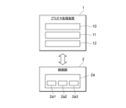
- FIG. 1 is a diagram for explaining a configuration example of a plasma processing system.
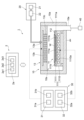
- FIG. 1 is a diagram for explaining a configuration example of a capacitively coupled plasma processing apparatus.
- 1 is a flowchart illustrating an example of a plasma processing method.
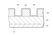
- 2 is a diagram showing an example of a cross-sectional structure of a substrate W provided in a process ST1.
- FIG. 10A and 10B are diagrams for explaining an example of supply of a processing gas, supply of a source RF signal, and supply of a bias RF signal in step ST2.
- 10 is a diagram for explaining an example of a cross-sectional structure of the substrate W in a first period S1 of process ST2.
- FIG. 1 is a diagram for explaining a configuration example of a plasma processing system.
- FIG. 1 is a diagram for explaining a configuration example of a capacitively coupled plasma processing apparatus.
- 1 is a flowchart illustrating an example of a plasma processing method.
- 2 is a diagram showing an example
- FIG. 10 is a diagram for explaining an example of a cross-sectional structure of the substrate W in a second period S2 of process ST2.
- FIG. 10 is a diagram for explaining an example of a cross-sectional structure of the substrate W in a third period S3 of process ST2.
- FIG. 10A and 10B are diagrams for explaining an example of supply of a processing gas, supply of a source RF signal, and supply of a bias DC signal in step ST2.
- a plasma processing method includes: (a) providing a substrate including a film to be etched and a resist film on the film to be etched to a substrate support in a chamber, the resist film including a pattern having an opening; and (b) forming a deposition film on at least a portion of a surface of the substrate using a plasma generated from a process gas before etching the film to be etched, the method including repeating a cycle including a first period of supplying a source RF signal having a first power level to the chamber and supplying a bias signal having a second power level to the substrate support; a second period of supplying a source RF signal having a third power level less than the first power level to the chamber and supplying a bias signal having a fourth power level greater than the second power level to the substrate support; and a third period of supplying a source RF signal having a fifth power level less than the third power level to the chamber and supplying a bias signal having a sixth power level greater than the
- the process gas is continuously supplied into the chamber during the first period, the second period, and the third period in step (b).
- the process gas includes a deposition gas for forming the deposition film and a trim gas for removing the deposition film.
- the deposition gas includes a carbon-containing gas.
- the deposition gas includes at least one gas selected from the group consisting of CO gas, CH-based gas, CHF-based gas, and CF-based gas.
- the trim gas comprises at least one selected from the group consisting of N2 gas, O2 gas, CO2 gas, and CO gas.
- the resist film includes an EUV resist film.
- the EUV resist film includes a metal.
- the metal is tin.
- the second power level of the bias signal is a zero power level.
- the fifth power level of the source RF signal is a zero power level.
- the third period is shorter than the first period.
- the cycle has a period within the range of 0.01 msec to 10 msec.
- the bias signal is an RF signal or a DC voltage pulse signal.
- the DC voltage pulse signal comprises a sequence of voltage pulses having negative polarity voltage levels.
- the chamber includes an upper electrode disposed above the substrate support, and the source RF signal is provided to the upper electrode.
- the process gas is a gas that includes CO gas and N2 gas.
- the process gas is a gas consisting of CO gas and N2 gas.
- a chamber, a substrate support provided in the chamber, a plasma generating unit, a gas supply unit, and a control unit are provided, and the control unit executes the following operations: (a) controlling a substrate including a film to be etched and a resist film on the film to be etched to the substrate support in the chamber, the resist film including a pattern having an opening; and (b) controlling a deposition film to be formed on at least a portion of a surface of the substrate using plasma generated from a process gas before etching the film to be etched, and removing at least a portion of the deposition film, and (b) controlling a source RF signal having a first power level.
- a plasma processing apparatus repeats a cycle including a first period during which a source RF signal is supplied to the chamber and a bias signal having a second power level is supplied to the substrate support, a second period during which a source RF signal is supplied to the chamber and a bias signal having a fourth power level greater than the second power level is supplied to the substrate support, and a third period during which a source RF signal is supplied to the chamber and a bias signal having a fifth power level less than the third power level is supplied to the substrate support.
- FIG. 1 is a diagram for explaining a configuration example of a plasma processing system.
- the plasma processing system includes a plasma processing device 1 and a control unit 2.
- the plasma processing system is an example of a substrate processing system
- the plasma processing device 1 is an example of a substrate processing device.
- the plasma processing device 1 includes a plasma processing chamber 10, a substrate support unit 11, and a plasma generation unit 12.
- the plasma processing chamber 10 has a plasma processing space.
- the plasma processing chamber 10 also has at least one gas supply port for supplying at least one processing gas to the plasma processing space, and at least one gas exhaust port for exhausting gas from the plasma processing space.
- the gas supply port is connected to a gas supply unit 20 described later, and the gas exhaust port is connected to an exhaust system 40 described later.
- the substrate support unit 11 is disposed in the plasma processing space, and has a substrate support surface for supporting a substrate.
- the plasma generating unit 12 is configured to generate plasma from at least one processing gas supplied into the plasma processing space.
- the plasma formed in the plasma processing space may be capacitively coupled plasma (CCP), inductively coupled plasma (ICP), ECR plasma (Electron-Cyclotron-resonance plasma), Helicon wave excited plasma (HWP), or surface wave plasma (SWP), etc.
- various types of plasma generating units may be used, including AC (Alternating Current) plasma generating units and DC (Direct Current) plasma generating units.
- the AC signal (AC power) used in the AC plasma generating unit has a frequency in the range of 100 kHz to 10 GHz.
- AC signals include RF (Radio Frequency) signals and microwave signals.
- the RF signal has a frequency in the range of 100 kHz to 150 MHz.
- the control unit 2 processes computer-executable instructions that cause the plasma processing apparatus 1 to perform the various steps described in this disclosure.
- the control unit 2 may be configured to control each element of the plasma processing apparatus 1 to perform the various steps described herein. In one embodiment, a part or all of the control unit 2 may be included in the plasma processing apparatus 1.
- the control unit 2 may include a processing unit 2a1, a storage unit 2a2, and a communication interface 2a3.
- the control unit 2 is realized, for example, by a computer 2a.
- the processing unit 2a1 may be configured to perform various control operations by reading a program from the storage unit 2a2 and executing the read program. This program may be stored in the storage unit 2a2 in advance, or may be acquired via a medium when necessary.
- the acquired program is stored in the storage unit 2a2 and is read from the storage unit 2a2 by the processing unit 2a1 and executed.
- the medium may be various storage media readable by the computer 2a, or may be a communication line connected to the communication interface 2a3.
- the processing unit 2a1 may be a CPU (Central Processing Unit).
- the memory unit 2a2 may include a RAM (Random Access Memory), a ROM (Read Only Memory), a HDD (Hard Disk Drive), a SSD (Solid State Drive), or a combination of these.
- the communication interface 2a3 may communicate with the plasma processing device 1 via a communication line such as a LAN (Local Area Network).
- FIG. 1 is a diagram for explaining a configuration example of a capacitively coupled plasma processing device.
- the capacitively coupled plasma processing apparatus 1 includes a plasma processing chamber 10, a gas supply unit 20, a power supply 30, and an exhaust system 40.
- the plasma processing apparatus 1 also includes a substrate support unit 11 and a gas inlet unit.
- the gas inlet unit is configured to introduce at least one processing gas into the plasma processing chamber 10.
- the gas inlet unit includes a shower head 13.
- the substrate support unit 11 is disposed in the plasma processing chamber 10.
- the shower head 13 is disposed above the substrate support unit 11. In one embodiment, the shower head 13 constitutes at least a part of the ceiling of the plasma processing chamber 10.
- the plasma processing chamber 10 has a plasma processing space 10s defined by the shower head 13, the sidewall 10a of the plasma processing chamber 10, and the substrate support unit 11.
- the plasma processing chamber 10 is grounded.
- the shower head 13 and the substrate support unit 11 are electrically insulated from the housing of the plasma processing chamber 10.
- the substrate support 11 includes a main body 111 and a ring assembly 112.
- the main body 111 has a central region 111a for supporting the substrate W and an annular region 111b for supporting the ring assembly 112.
- a wafer is an example of a substrate W.
- the annular region 111b of the main body 111 surrounds the central region 111a of the main body 111 in a plan view.
- the substrate W is disposed on the central region 111a of the main body 111
- the ring assembly 112 is disposed on the annular region 111b of the main body 111 so as to surround the substrate W on the central region 111a of the main body 111. Therefore, the central region 111a is also called a substrate support surface for supporting the substrate W, and the annular region 111b is also called a ring support surface for supporting the ring assembly 112.
- the main body 111 includes a base 1110 and an electrostatic chuck 1111.
- the base 1110 includes a conductive member.
- the conductive member of the base 1110 may function as a lower electrode.
- the electrostatic chuck 1111 is disposed on the base 1110.
- the electrostatic chuck 1111 includes a ceramic member 1111a and an electrostatic electrode 1111b disposed within the ceramic member 1111a.
- the ceramic member 1111a has a central region 111a. In one embodiment, the ceramic member 1111a also has an annular region 111b. Note that other members surrounding the electrostatic chuck 1111, such as an annular electrostatic chuck or an annular insulating member, may have the annular region 111b.
- the ring assembly 112 may be disposed on the annular electrostatic chuck or the annular insulating member, or may be disposed on both the electrostatic chuck 1111 and the annular insulating member.
- At least one RF/DC electrode coupled to an RF power source 31 and/or a DC power source 32, which will be described later, may be disposed within the ceramic member 1111a.
- the at least one RF/DC electrode functions as a lower electrode.
- the RF/DC electrode is also called a bias electrode.
- the conductive member of the base 1110 and the at least one RF/DC electrode may function as multiple lower electrodes.
- the electrostatic electrode 1111b may function as a lower electrode.
- the substrate support 11 includes at least one lower electrode.
- the ring assembly 112 includes one or more annular members.
- the one or more annular members include one or more edge rings and at least one cover ring.
- the edge rings are formed of a conductive or insulating material, and the cover rings are formed of an insulating material.
- the substrate support 11 may also include a temperature adjustment module configured to adjust at least one of the electrostatic chuck 1111, the ring assembly 112, and the substrate to a target temperature.
- the temperature adjustment module may include a heater, a heat transfer medium, a flow passage 1110a, or a combination thereof.
- a heat transfer fluid such as brine or a gas flows through the flow passage 1110a.
- the flow passage 1110a is formed in the base 1110, and one or more heaters are disposed in the ceramic member 1111a of the electrostatic chuck 1111.
- the substrate support 11 may also include a heat transfer gas supply configured to supply a heat transfer gas to a gap between the back surface of the substrate W and the central region 111a.
- the shower head 13 is configured to introduce at least one processing gas from the gas supply unit 20 into the plasma processing space 10s.
- the shower head 13 has at least one gas supply port 13a, at least one gas diffusion chamber 13b, and multiple gas inlets 13c.
- the processing gas supplied to the gas supply port 13a passes through the gas diffusion chamber 13b and is introduced into the plasma processing space 10s from the multiple gas inlets 13c.
- the shower head 13 also includes at least one upper electrode.
- the gas introduction unit may include, in addition to the shower head 13, one or more side gas injectors (SGI) attached to one or more openings formed in the side wall 10a.
- SGI side gas injectors
- the gas supply unit 20 may include at least one gas source 21 and at least one flow controller 22.
- the gas supply unit 20 is configured to supply at least one process gas from a respective gas source 21 through a respective flow controller 22 to the showerhead 13.
- Each flow controller 22 may include, for example, a mass flow controller or a pressure-controlled flow controller.
- the gas supply unit 20 may include at least one flow modulation device that modulates or pulses the flow rate of the at least one process gas.
- the power supply 30 includes an RF power supply 31 coupled to the plasma processing chamber 10 via at least one impedance matching circuit.
- the RF power supply 31 is configured to supply at least one RF signal (RF power) to at least one lower electrode and/or at least one upper electrode. This causes a plasma to be formed from at least one processing gas supplied to the plasma processing space 10s.
- the RF power supply 31 can function as at least a part of the plasma generating unit 12.
- a bias RF signal to at least one lower electrode, a bias potential is generated on the substrate W, and ion components in the formed plasma can be attracted to the substrate W.
- the RF power supply 31 includes a first RF generating unit 31a and a second RF generating unit 31b.
- the first RF generating unit 31a is coupled to at least one lower electrode and/or at least one upper electrode via at least one impedance matching circuit and configured to generate a source RF signal (source RF power) for plasma generation.
- the source RF signal has a frequency in the range of 10 MHz to 150 MHz.
- the first RF generating unit 31a may be configured to generate multiple source RF signals having different frequencies. The generated one or more source RF signals are supplied to at least one lower electrode and/or at least one upper electrode.
- the second RF generator 31b is coupled to at least one lower electrode via at least one impedance matching circuit and configured to generate a bias RF signal (bias RF power).
- the frequency of the bias RF signal may be the same as or different from the frequency of the source RF signal.
- the bias RF signal has a lower frequency than the frequency of the source RF signal.
- the bias RF signal has a frequency in the range of 100 kHz to 60 MHz.
- the second RF generator 31b may be configured to generate multiple bias RF signals having different frequencies.
- the generated one or more bias RF signals are provided to at least one lower electrode. Also, in various embodiments, at least one of the source RF signal and the bias RF signal may be pulsed.
- the power supply 30 may also include a DC power supply 32 coupled to the plasma processing chamber 10.
- the DC power supply 32 includes a first DC generator 32a and a second DC generator 32b.
- the first DC generator 32a is connected to at least one lower electrode and configured to generate a first DC signal.
- the generated first DC signal is applied to the at least one lower electrode.
- the second DC generator 32b is connected to at least one upper electrode and configured to generate a second DC signal.
- the generated second DC signal is applied to the at least one upper electrode.
- the first and second DC signals may be pulsed.
- a sequence of voltage pulses is applied to at least one lower electrode and/or at least one upper electrode.
- the voltage pulses may have a rectangular, trapezoidal, triangular or combination thereof pulse waveform.
- a waveform generator for generating a sequence of voltage pulses from the DC signal is connected between the first DC generator 32a and at least one lower electrode.
- the first DC generator 32a and the waveform generator constitute a voltage pulse generator.
- the second DC generator 32b and the waveform generator constitute a voltage pulse generator
- the voltage pulse generator is connected to at least one upper electrode.
- the voltage pulses may have a positive polarity or a negative polarity.
- the sequence of voltage pulses may include one or more positive polarity voltage pulses and one or more negative polarity voltage pulses within one period.
- the first and second DC generating units 32a and 32b may be provided in addition to the RF power source 31, or the first DC generating unit 32a may be provided in place of the second RF generating unit 31b.
- the exhaust system 40 may be connected to, for example, a gas exhaust port 10e provided at the bottom of the plasma processing chamber 10.
- the exhaust system 40 may include a pressure regulating valve and a vacuum pump. The pressure in the plasma processing space 10s is adjusted by the pressure regulating valve.
- the vacuum pump may include a turbomolecular pump, a dry pump, or a combination thereof.
- ⁇ An example of a plasma treatment method> 3 is a flowchart showing an example of a plasma processing method (hereinafter also referred to as "the method") according to an illustrative embodiment.
- the method includes a step ST1 of providing a substrate W, and a step ST2 of forming a deposition film on the surface of the substrate W and removing a part of the deposition film.
- the processing in each step may be performed in a plasma processing apparatus 1 (see FIG. 2).
- a control unit 2 controls each part of the plasma processing apparatus 1 to perform the method.
- the substrate W may be provided in a plasma processing space 10s of the plasma processing apparatus 1.
- the substrate W is provided in a central region 111a of the substrate support 11 and held on the substrate support 11 by an electrostatic chuck 1111.
- FIG. 4 is a diagram for explaining an example of the cross-sectional structure of the substrate W provided in process ST1.
- the substrate W has a film to be etched EF and a resist film (resist pattern) RP including a pattern formed on the film to be etched EF.
- the film to be etched EF and the resist film RP may be formed on an undercoat film UF.
- the substrate W may be used in the manufacture of semiconductor devices.
- the semiconductor devices include, for example, semiconductor memory devices such as DRAMs and 3D-NAND flash memories.
- the base film UF may be a silicon wafer or an organic film, a dielectric film, a metal film, a semiconductor film, or the like formed on a silicon wafer.
- the base film UF may be configured by stacking multiple films.
- the film to be etched EF is a film that is to be etched.
- the film to be etched EF may be, for example, an organic film, a dielectric film, a semiconductor film, or a metal film.
- the film to be etched EF may be composed of a single film, or may be composed of a stack of multiple films.
- the film to be etched EF may be composed of one or more stacks of films such as a silicon-containing film, a carbon-containing film, a spin-on-glass (SOG) film, or a Si-containing antireflective film (SiARC).
- the resist film RP includes a film that functions as a mask in etching the film EF to be etched.
- the resist film RP may be an organic film.
- the resist film RP may include an EUV (Extreme Ultraviolet) resist film or an ArF resist film.
- the resist film (photoresist film) PR may be a metal-containing film.
- the metal-containing film is a film containing tin.
- the resist film PR may contain at least one of tin oxide and tin hydroxide.
- the tin-containing film may contain an organic substance.
- the resist film RP may be composed of one film, or may be composed of a plurality of films stacked together. In one embodiment, as shown in FIG. 4, the film surface of the resist film RP of the substrate W provided in step ST1 may have irregularities.
- the resist film RP may have dimensions smaller than the design dimensions.
- the pattern of the resist film RP may include at least one opening OP on the film EF to be etched.
- the opening OP may be defined by the side of the resist film RP.
- the film EF to be etched may be exposed at the bottom of the opening OP. That is, the upper surface of the film EF to be etched may have an area covered by the resist film RP and an area exposed at the bottom of the opening OP.
- the openings OP may have any shape when viewed from above the substrate W, i.e., when the substrate W is viewed from the top to the bottom in FIG. 4.
- the shape may be, for example, a circle, an ellipse, a rectangle, a line, or a combination of one or more of these.
- the resist film RP may have multiple side walls that define multiple openings OP.
- the multiple openings OP may each have a linear shape and be arranged at regular intervals to form a line-and-space pattern.
- the multiple openings OP may also each have a hole shape and form an array pattern.
- Each film constituting the substrate W may be formed by a CVD method, an ALD method, a spin coating method, or the like.
- the pattern of the resist film RP may be formed by lithography. Lithography may be performed using an EUV light source or an ArF light source.
- the temperature of the substrate support 11 or the substrate W may be set to a predetermined temperature.
- the temperature of the substrate support 11 or the substrate W is adjusted to a set temperature by a temperature control module.
- adjusting or maintaining the temperature of the substrate support 11 or the substrate W includes adjusting or maintaining the temperature of the heat transfer fluid flowing through the flow path 1110a to a set temperature or a temperature different from the set temperature.
- adjusting or maintaining the temperature of the substrate support 11 or the substrate W includes controlling the pressure of the heat transfer gas (e.g., He) between the electrostatic chuck 1111 and the back surface of the substrate W.
- the heat transfer gas e.g., He
- the timing at which the heat transfer fluid starts to flow through the flow path 1110a may be before or after the substrate W is placed on the substrate support 11, or may be the same as the substrate W.
- the temperature of the substrate support 11 or the substrate W may also be adjusted before step ST1. That is, the temperature of the substrate support 11 or the substrate W may be adjusted to a set temperature before the substrate support 11 is provided with the substrate W.
- Step ST2 forming a deposition film on the surface of the substrate and removing a part of the deposition film
- a deposition film may be formed on at least a part of the surface of the substrate W, and at least a part of the deposition film may be removed, using plasma generated from the processing gas.
- a cycle C1 including a first period S1, a second period S2, and a third period S3 in this order is repeated a predetermined number of times.
- a processing gas is supplied from the gas supply unit 20 shown in FIG. 2 into the plasma processing space 10s.
- a source RF signal is supplied from the RF power supply 31 to the lower electrode of the substrate support 11 and/or the upper electrode of the shower head 13. This generates a high-frequency electric field between the shower head 13 and the substrate support 11, and plasma is generated from the processing gas in the plasma processing space 10s.
- a bias signal is supplied to the lower electrode of the substrate support 11.
- the bias signal may be a bias RF signal supplied from the RF power supply 31 or a bias DC signal supplied from the DC power supply 32.
- FIG. 5 is a diagram for explaining an example of the supply of processing gas, the supply of a source RF signal, and the supply of a bias RF signal in step ST2.
- processing gas may be continuously supplied during the entire first period S1, the second period S2, and the third period S3.
- the processing gas may include a deposition gas for forming a deposition film and a trim gas for removing the deposition film.
- the deposition gas may include a carbon-containing gas.
- the deposition gas may include at least one selected from the group consisting of CO gas, CH -based gas , CHF - based gas, and CF-based gas.
- the CH-based gas (hydrocarbon gas) may include at least one selected from the group consisting of CH4 gas, C2H2 gas, C2H4 gas, and C3H6 gas.
- the CHF-based (hydrofluorocarbon gas) may include at least one selected from the group consisting of CH2F2 gas, CH3F gas, and CHF3 gas .
- the CF-based gas may include at least one selected from the group consisting of CF4 gas, C2F2 gas , C2F4 gas , C3F6 gas , C3F8 gas , C4F6 gas, C4F8 gas , and C5F8 gas.
- the trim gas may include at least one selected from the group consisting of N2 gas, O2 gas, CO2 gas, and CO gas.
- the process gas may further include a rare gas such as Ar gas.
- the process gas may include CO gas and N2 gas.
- the process gas may consist of CO gas and N2 gas.
- a source RF signal having a first power level P1 may be supplied to the upper electrode of the chamber 10, and a bias RF signal having a second power level P2 may be supplied to the lower electrode of the substrate support 11.
- the second power level P2 may be a zero power level (OFF).
- FIG. 6 is a diagram for explaining an example of the cross-sectional structure of the substrate W in the first period S1.
- ions and radicals generated from the deposition gas of the processing gas are deposited on the surface of the substrate W to form a deposited film DF.
- the deposited film DF may be formed on the surface of the resist film RP (the film upper surface and the side surface defining the opening OP) or the bottom surface of the opening OP where the film to be etched EF is exposed.
- a source RF signal having a third power level P3 less than the first power level P1 may be supplied to the upper electrode of the chamber 10, and a bias RF signal having a fourth power level P4 greater than the second power level P2 may be supplied to the lower electrode of the substrate support 11.
- FIG. 7 is a diagram for explaining an example of the cross-sectional structure of the substrate W in the second period S2.
- ions are attracted to the surface of the substrate W, and react with the deposited film DF on the surface of the resist film RP, causing the deposited film DF to become carbon-rich and harden, thereby modifying the deposited film DF.
- the generation of ions and radicals is suppressed more in the second period S2 than in the first period S1, and the formation of a new deposited film DF on the surface of the resist film RP is suppressed.
- a source RF signal having a fifth power level P5 less than the third power level P3 may be supplied to the upper electrode of the chamber 10, and a bias RF signal having a sixth power level P6 greater than the fourth power level P4 may be supplied to the lower electrode of the substrate support 11.
- the fifth power level P5 may be a zero power level (OFF).
- the third period S3 may be shorter than the first period S1.
- the third period S3 may be shorter than the second period S2.
- FIG. 8 is a diagram for explaining an example of the cross-sectional structure of the substrate W in the third period S3.
- ions generated from the trim gas of the processing gas may be drawn toward the substrate W, and a portion of the deposited film DF on the surface of the resist film RP may be removed. This may bring the resist film PR closer to the design dimensions.
- the deposited film DF on the bottom surface of the opening OP may be removed. This may re-expose a portion of the surface of the film to be etched EF to the opening OP.
- the generation of ions and radicals is suppressed more than in the first period S1.
- the temperature of the ions is reduced. This causes the ions to be drawn vertically into the opening OP.
- the cycle C1 including the first period S1, the second period S2, and the third period S3 may be repeated a predetermined number of times, after which the process ST2 ends.
- the cycle C1 may be repeated 100 times or more, 150 times or more, 1000 times or more, 5000 times or more, 10000 times or more, or 2 million times or less.
- the cycle C1 may have a period within a range of 0.01 msec to 10 msec.
- the film EF to be etched may be subsequently etched.
- the etching of the film EF to be etched may be performed in the same plasma processing apparatus or in another plasma processing apparatus.
- the etching of the film EF to be etched may be performed using plasma generated from a processing gas.
- the processing gas used in etching the film EF to be etched may have a different gas species than the processing gas used in step ST2.
- the plasma processing method includes: (a) a step of providing a substrate W including a film EF to be etched and a resist film RP having a pattern on the film EF to be etched to a substrate support 11 in a chamber 10 (step ST1); and (b) a step of forming a deposited film DF on at least a portion of a surface of the substrate W using plasma generated from a processing gas and removing at least a portion of the deposited film DF before etching the film EF to be etched (step ST2).
- step ST2 repeats a cycle C1 including a first period S1 in which a source RF signal having a first power level P1 is supplied to the chamber 10 and a bias signal having a second power level P2 is supplied to the substrate support part 11, a second period S2 in which a source RF signal having a third power level P3 smaller than the first power level P1 is supplied to the chamber 10 and a bias signal having a fourth power level P4 larger than the second power level P2 is supplied to the substrate support part 11, and a third period S3 in which a source RF signal having a fifth power level P5 smaller than the third power level P3 is supplied to the chamber 10 and a bias signal having a sixth power level P6 larger than the fourth power level P4 is supplied to the substrate support part 11.
- the shape of the resist pattern to be improved.
- the time required for the plasma processing to improve the shape of the resist pattern can be shortened. This allows the throughput of the plasma processing to be improved.
- the deposition film DF formed on the surface of the resist film RP is modified, thereby improving the localized uniformity (LCDU) of the shape of the resist pattern.
- the condition before the transition to the third period S3 can be adjusted.
- the plasma can be maintained and the amount and type of ions and radicals can be adjusted.
- This adjustment of the amount and type of ions and radicals may include adjusting the dissociation amount of the trim gas.
- the organic material deposition film DF
- the carbon ratio of the deposition film DF may be increased or the mixing of the resist film RP and the deposition gas may be promoted. This makes it possible to adjust the shape of the deposition film DF and promote the deposition of the deposition film DF to the sidewall of a pattern with a large line width.
- the processing gas is continuously supplied into the chamber 10, so that the processing gas is not switched (ON/OFF), and as a result, the plasma processing can be performed in a short time.
- the third period S3 is shorter than the first period S1, so that ions can be prevented from damaging the film on the substrate surface during the third period S3.
- the bias signal supplied to the substrate support 11 may be a bias DC signal.
- the bias DC signal may be a DC voltage pulse signal.
- the DC voltage pulse signal may be supplied from the DC power supply 32 to the lower electrode of the substrate support 11.
- the DC voltage pulse signal may have a sequence of voltage pulses having a negative voltage level.
- FIG. 9 is a diagram for explaining an example of the supply of the process gas, the supply of the source RF signal, and the supply of the bias DC signal in the process ST2.
- the DC voltage pulse signal which is the bias DC signal, may have a sequence of voltage pulses in the second period S2 and the third period S3 of the cycle C1.
- the sequence of the voltage pulses in the second period S2 may have a voltage level V1 corresponding to the fourth power level P4, and the sequence of the voltage pulses in the third period S3 may have a voltage level V2 corresponding to the sixth power level P6.
- the DC voltage pulse signal may have a reference voltage level Vref corresponding to the second power level P2 in the first period S2.
- the reference voltage level Vref may be a zero voltage level.
- the voltage level V1 in the second period S2 and the voltage level V2 in the third period S3 may have negative polarity.
- the absolute value of the voltage level V2 in the third period S3 may be greater than the absolute value of the voltage level V1 in the second period S2.
- a capacitively coupled plasma device has been described as an example, but the present invention is not limited to this and may be applied to other plasma devices.
- an inductively coupled plasma device may be used instead of a capacitively coupled plasma device.
- step (b) comprises: a first time period providing a source RF signal having a first power level to the chamber and a bias signal having a second power level to the substrate support; a second time period providing the source RF signal to the chamber having a third power level less than the first power level and providing the bias signal to the substrate support having a fourth power level greater than the second power level; a third period of time during which the source RF signal is supplied to the chamber having a fifth power level that is less than the third power level and the bias signal is supplied to the substrate support having a sixth power level that is greater than the fourth
- the process gas includes a deposition gas for forming the deposition film and a trim gas for removing the deposition film; 3.
- the deposition gas comprises a carbon-containing gas. 4. The plasma processing method according to claim 3.
- the deposition gas includes at least one gas selected from the group consisting of CO gas, CH-based gas, CHF-based gas, and CF-based gas. 4. The plasma processing method according to claim 3.
- the trim gas includes at least one selected from the group consisting of N2 gas, O2 gas, CO2 gas, and CO gas; 6.
- the resist film includes an EUV resist film. 7.
- the plasma processing method according to claim 1 The plasma processing method according to claim 1 .
- the EUV resist film contains a metal. 8. The plasma processing method according to claim 7.
- the cycle has a period within a range of 0.01 msec to 10 msec. 13.
- the plasma processing method according to any one of claims 1 to 12.
- the bias signal is an RF signal or a DC voltage pulse signal. 14.
- the plasma processing method according to any one of claims 1 to 13.
- the DC voltage pulse signal comprises a sequence of voltage pulses having negative polarity voltage levels; 15.
- the chamber includes an upper electrode disposed above the substrate support;
- the source RF signal is provided to the upper electrode.
- the plasma processing method according to any one of claims 1 to 15.
- the processing gas is a gas containing CO gas and N2 gas; 17.
- the plasma processing method according to any one of claims 1 to 16.
- the processing gas is a gas consisting of CO gas and N2 gas. 17.
- the plasma processing method according to any one of claims 1 to 16.
- the method includes the steps of: providing a chamber; and providing a substrate support unit, a plasma generating unit, a gas supply unit, and a control unit in the chamber;
- the control unit is (a) controlling a substrate including a film to be etched and a resist film on the film to be etched, the resist film including a pattern having an opening; (b) before etching the etching target film, performing control to form a deposition film on at least a portion of a surface of the substrate using plasma generated from a processing gas, and to remove at least a portion of the deposition film;
- the (b) control is a first time period providing a source RF signal having a first power level to the chamber and a bias signal having a second power level to the substrate support; a second time period providing the source RF signal to the chamber having a third power level less than the first power level and providing the bias signal to the substrate support having a fourth power level greater than the second power level; a third period of time during which the source RF signal is
- Reference Signs List 1 Plasma processing apparatus, 2: Control unit, 10: Chamber, 11: Substrate support unit, 12: Plasma generation unit, 20: Gas supply unit, RP: Resist film, EF: Film to be etched, DF: Deposited film, W: Substrate
Landscapes
- Physics & Mathematics (AREA)
- Engineering & Computer Science (AREA)
- Plasma & Fusion (AREA)
- Chemical & Material Sciences (AREA)
- Analytical Chemistry (AREA)
- General Physics & Mathematics (AREA)
- Drying Of Semiconductors (AREA)
- Physical Vapour Deposition (AREA)
Priority Applications (5)
| Application Number | Priority Date | Filing Date | Title |
|---|---|---|---|
| JP2025510226A JPWO2024203220A1 (https=) | 2023-03-24 | 2024-03-11 | |
| KR1020257033694A KR20250164230A (ko) | 2023-03-24 | 2024-03-11 | 플라즈마 처리 방법 및 플라즈마 처리 장치 |
| CN202480018771.5A CN120814029A (zh) | 2023-03-24 | 2024-03-11 | 等离子体处理方法和等离子体处理装置 |
| TW113109598A TW202439445A (zh) | 2023-03-24 | 2024-03-15 | 電漿處理方法及電漿處理裝置 |
| US19/328,251 US20260011556A1 (en) | 2023-03-24 | 2025-09-15 | Plasma processing method and plasma processing apparatus |
Applications Claiming Priority (2)
| Application Number | Priority Date | Filing Date | Title |
|---|---|---|---|
| JP2023048053 | 2023-03-24 | ||
| JP2023-048053 | 2023-03-24 |
Related Child Applications (1)
| Application Number | Title | Priority Date | Filing Date |
|---|---|---|---|
| US19/328,251 Continuation US20260011556A1 (en) | 2023-03-24 | 2025-09-15 | Plasma processing method and plasma processing apparatus |
Publications (1)
| Publication Number | Publication Date |
|---|---|
| WO2024203220A1 true WO2024203220A1 (ja) | 2024-10-03 |
Family
ID=92904447
Family Applications (1)
| Application Number | Title | Priority Date | Filing Date |
|---|---|---|---|
| PCT/JP2024/009310 Ceased WO2024203220A1 (ja) | 2023-03-24 | 2024-03-11 | プラズマ処理方法及びプラズマ処理装置 |
Country Status (6)
| Country | Link |
|---|---|
| US (1) | US20260011556A1 (https=) |
| JP (1) | JPWO2024203220A1 (https=) |
| KR (1) | KR20250164230A (https=) |
| CN (1) | CN120814029A (https=) |
| TW (1) | TW202439445A (https=) |
| WO (1) | WO2024203220A1 (https=) |
Citations (4)
| Publication number | Priority date | Publication date | Assignee | Title |
|---|---|---|---|---|
| JP2007503720A (ja) * | 2003-08-26 | 2007-02-22 | ラム リサーチ コーポレーション | フィーチャ微小寸法の低減 |
| JP2009530861A (ja) * | 2006-03-24 | 2009-08-27 | アプライド マテリアルズ インコーポレイテッド | 介在チャンバでの脱フッ素化及びウェハ脱フッ素化ステップによるプラズマエッチング及びフォトレジストストリッププロセス |
| JP2020077753A (ja) * | 2018-11-07 | 2020-05-21 | 東京エレクトロン株式会社 | 処理方法及び基板処理装置 |
| JP2022544480A (ja) * | 2019-08-14 | 2022-10-19 | 東京エレクトロン株式会社 | プラズマ処理のための3フェーズパルス印加システム及び方法 |
Family Cites Families (1)
| Publication number | Priority date | Publication date | Assignee | Title |
|---|---|---|---|---|
| US10727075B2 (en) | 2017-12-22 | 2020-07-28 | Applied Materials, Inc. | Uniform EUV photoresist patterning utilizing pulsed plasma process |
-
2024
- 2024-03-11 JP JP2025510226A patent/JPWO2024203220A1/ja active Pending
- 2024-03-11 CN CN202480018771.5A patent/CN120814029A/zh active Pending
- 2024-03-11 WO PCT/JP2024/009310 patent/WO2024203220A1/ja not_active Ceased
- 2024-03-11 KR KR1020257033694A patent/KR20250164230A/ko active Pending
- 2024-03-15 TW TW113109598A patent/TW202439445A/zh unknown
-
2025
- 2025-09-15 US US19/328,251 patent/US20260011556A1/en active Pending
Patent Citations (4)
| Publication number | Priority date | Publication date | Assignee | Title |
|---|---|---|---|---|
| JP2007503720A (ja) * | 2003-08-26 | 2007-02-22 | ラム リサーチ コーポレーション | フィーチャ微小寸法の低減 |
| JP2009530861A (ja) * | 2006-03-24 | 2009-08-27 | アプライド マテリアルズ インコーポレイテッド | 介在チャンバでの脱フッ素化及びウェハ脱フッ素化ステップによるプラズマエッチング及びフォトレジストストリッププロセス |
| JP2020077753A (ja) * | 2018-11-07 | 2020-05-21 | 東京エレクトロン株式会社 | 処理方法及び基板処理装置 |
| JP2022544480A (ja) * | 2019-08-14 | 2022-10-19 | 東京エレクトロン株式会社 | プラズマ処理のための3フェーズパルス印加システム及び方法 |
Also Published As
| Publication number | Publication date |
|---|---|
| US20260011556A1 (en) | 2026-01-08 |
| CN120814029A (zh) | 2025-10-17 |
| TW202439445A (zh) | 2024-10-01 |
| JPWO2024203220A1 (https=) | 2024-10-03 |
| KR20250164230A (ko) | 2025-11-24 |
Similar Documents
| Publication | Publication Date | Title |
|---|---|---|
| JP2024006972A (ja) | プラズマ処理方法及びプラズマ処理システム | |
| CN117099189A (zh) | 蚀刻方法和等离子体处理装置 | |
| WO2024203220A1 (ja) | プラズマ処理方法及びプラズマ処理装置 | |
| US20250372349A1 (en) | Plasma processing apparatus, power supply system, and etching method | |
| WO2025079458A1 (ja) | エッチング方法及びエッチング装置 | |
| WO2025004625A1 (ja) | エッチング方法及びプラズマ処理装置 | |
| US20260074166A1 (en) | Etching method, method for manufacturing dram capacitor, and plasma processing apparatus | |
| JP2025089743A (ja) | エッチング方法 | |
| WO2025150294A1 (ja) | 基板処理方法及び基板処理装置 | |
| WO2025182550A1 (ja) | エッチング方法及びエッチング装置 | |
| WO2024171888A1 (ja) | プラズマ処理方法及びプラズマ処理装置 | |
| WO2025142198A1 (ja) | エッチング方法及び基板処理装置 | |
| WO2024204321A1 (ja) | エッチング装置及びエッチング方法 | |
| JP2024130804A (ja) | プラズマ処理方法及びプラズマ処理装置 | |
| JP2024135093A (ja) | プラズマ処理装置 | |
| WO2025182678A1 (ja) | 基板処理方法及びプラズマ処理装置 | |
| WO2024180921A1 (ja) | エッチング方法及びプラズマ処理装置 | |
| WO2025126998A1 (ja) | エッチング方法及びエッチング装置 | |
| TW202603883A (zh) | 蝕刻方法及電漿處理系統 | |
| TW202503831A (zh) | 電漿處理裝置及電漿處理方法 | |
| JP2025026361A (ja) | エッチング方法及びプラズマ処理装置 | |
| WO2025177874A1 (ja) | プラズマエッチング装置及び基板処理装置 | |
| TW202607815A (zh) | 基板處理方法及電漿處理裝置 | |
| WO2024090252A1 (ja) | 基板処理方法及び基板処理装置 | |
| JP2024017869A (ja) | エッチング方法及び基板処理装置 |
Legal Events
| Date | Code | Title | Description |
|---|---|---|---|
| 121 | Ep: the epo has been informed by wipo that ep was designated in this application |
Ref document number: 24779350 Country of ref document: EP Kind code of ref document: A1 |
|
| WWE | Wipo information: entry into national phase |
Ref document number: 202480018771.5 Country of ref document: CN |
|
| ENP | Entry into the national phase |
Ref document number: 2025510226 Country of ref document: JP Kind code of ref document: A |
|
| WWE | Wipo information: entry into national phase |
Ref document number: 2025510226 Country of ref document: JP |
|
| ENP | Entry into the national phase |
Ref document number: 1020257033694 Country of ref document: KR Free format text: ST27 STATUS EVENT CODE: A-0-1-A10-A15-NAP-PA0105 (AS PROVIDED BY THE NATIONAL OFFICE) |
|
| WWE | Wipo information: entry into national phase |
Ref document number: KR1020257033694 Country of ref document: KR Ref document number: 1020257033694 Country of ref document: KR |
|
| WWP | Wipo information: published in national office |
Ref document number: 202480018771.5 Country of ref document: CN |
|
| NENP | Non-entry into the national phase |
Ref country code: DE |
|
| 122 | Ep: pct application non-entry in european phase |
Ref document number: 24779350 Country of ref document: EP Kind code of ref document: A1 |