WO2024201811A1 - 荷電粒子線装置 - Google Patents
荷電粒子線装置 Download PDFInfo
- Publication number
- WO2024201811A1 WO2024201811A1 PCT/JP2023/012891 JP2023012891W WO2024201811A1 WO 2024201811 A1 WO2024201811 A1 WO 2024201811A1 JP 2023012891 W JP2023012891 W JP 2023012891W WO 2024201811 A1 WO2024201811 A1 WO 2024201811A1
- Authority
- WO
- WIPO (PCT)
- Prior art keywords
- electrode
- charged particle
- lens
- magnetic
- magnetic field
- Prior art date
- Legal status (The legal status is an assumption and is not a legal conclusion. Google has not performed a legal analysis and makes no representation as to the accuracy of the status listed.)
- Ceased
Links
Images



Classifications
-
- H—ELECTRICITY
- H01—ELECTRIC ELEMENTS
- H01J—ELECTRIC DISCHARGE TUBES OR DISCHARGE LAMPS
- H01J37/00—Discharge tubes with provision for introducing objects or material to be exposed to the discharge, e.g. for the purpose of examination or processing thereof
- H01J37/02—Details
- H01J37/04—Arrangements of electrodes and associated parts for generating or controlling the discharge, e.g. electron-optical arrangement or ion-optical arrangement
- H01J37/06—Electron sources; Electron guns
- H01J37/065—Construction of guns or parts thereof
-
- H—ELECTRICITY
- H01—ELECTRIC ELEMENTS
- H01J—ELECTRIC DISCHARGE TUBES OR DISCHARGE LAMPS
- H01J37/00—Discharge tubes with provision for introducing objects or material to be exposed to the discharge, e.g. for the purpose of examination or processing thereof
- H01J37/02—Details
- H01J37/04—Arrangements of electrodes and associated parts for generating or controlling the discharge, e.g. electron-optical arrangement or ion-optical arrangement
- H01J37/06—Electron sources; Electron guns
-
- H—ELECTRICITY
- H01—ELECTRIC ELEMENTS
- H01J—ELECTRIC DISCHARGE TUBES OR DISCHARGE LAMPS
- H01J37/00—Discharge tubes with provision for introducing objects or material to be exposed to the discharge, e.g. for the purpose of examination or processing thereof
- H01J37/02—Details
- H01J37/04—Arrangements of electrodes and associated parts for generating or controlling the discharge, e.g. electron-optical arrangement or ion-optical arrangement
- H01J37/10—Lenses
- H01J37/14—Lenses magnetic
- H01J37/141—Electromagnetic lenses
-
- H—ELECTRICITY
- H01—ELECTRIC ELEMENTS
- H01J—ELECTRIC DISCHARGE TUBES OR DISCHARGE LAMPS
- H01J37/00—Discharge tubes with provision for introducing objects or material to be exposed to the discharge, e.g. for the purpose of examination or processing thereof
- H01J37/26—Electron or ion microscopes; Electron or ion diffraction tubes
- H01J37/28—Electron or ion microscopes; Electron or ion diffraction tubes with scanning beams
-
- H—ELECTRICITY
- H01—ELECTRIC ELEMENTS
- H01J—ELECTRIC DISCHARGE TUBES OR DISCHARGE LAMPS
- H01J2237/00—Discharge tubes exposing object to beam, e.g. for analysis treatment, etching, imaging
- H01J2237/04—Means for controlling the discharge
- H01J2237/047—Changing particle velocity
- H01J2237/0473—Changing particle velocity accelerating
- H01J2237/04735—Changing particle velocity accelerating with electrostatic means
Definitions
- This disclosure relates to a charged particle beam device.
- SEMs Scanning electron microscopes
- Semiconductor devices have extremely fine structures such as line patterns and holes, and if there are defects in these structures, the semiconductor device will not function properly.
- SEMs are suitable for inspecting semiconductor devices because they are capable of observing the shape and analyzing the components of nano-order microstructures.
- the first is high resolution to accommodate further miniaturization of semiconductor devices. Since semiconductor devices are composed of patterns with widths of tens to several nm, SEMs are also required to have a high resolution of several nm.
- the second is to accommodate the diversification of observation conditions to accommodate changes in the structure of semiconductor devices or their increasing complexity. For example, the structure of samples has become increasingly diverse due to the adoption of new materials and the introduction of high-density stacked structures such as 3D-NAND.
- the layer from which information can be obtained changes depending on the acceleration when electrons are bombarded into the sample, and the sample surface may be observed with a low-acceleration electron beam to prevent charging, or the structure of deep grooves may be observed with a high-acceleration electron beam. Therefore, it is necessary to be able to observe with a wide range of electron beams, from low to high acceleration.
- the third is improvement of inspection throughput. Even if the structure of samples becomes finer and denser and the number of inspection points on one sample increases, it is required to suppress the extension of inspection time as much as possible or to shorten the inspection time.
- the scanning speed of the electron beam is increased to increase the imaging speed, the number of electrons shot into the sample per pixel decreases, increasing the noise components in the SEM image and reducing the resolution.
- the amount of current in the electron beam is necessary to increase the amount of current in the electron beam.
- the fourth is the stability of inspection accuracy. To prevent variation in the inspection results, the current emitted from the electron source must be stable even when the SEM is operated continuously for long periods of time.
- Magnetic field superposition is known as a method for achieving both high resolution and large current.
- Magnetic field superposition is a method in which a magnetic field lens 105, which is used as a condenser lens in an electron optical system, and an electron source 101 are placed close to each other.
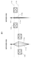
- Figure 1 shows a schematic diagram of the spread of an electron beam directly below the electron source 101.
- Electron beams 110 and 111 show the trajectories of the electron beam when the aperture amount is relatively large and small, respectively.
- the trajectory of the electron beam spreads significantly by the time it reaches the principal surface position 112 where the magnetic field lens 105 acts on the electron beam from the electron source 101.
- a characteristic of magnetic lenses is that the magnetic field is not uniform on the optical axis and at locations away from the optical axis. This causes aberration to occur between electrons that pass through the center of the magnetic lens and those that pass through its outside. For this reason, the effect of the aberration of the magnetic field lens 105 becomes significant, particularly when the aperture amount is reduced (high current, electron beam 111a).
- Patent Document 1 discloses a structure in which a magnetic lens is arranged to overlap the tip of a thermionic electron source in order to improve resolution.
- the electron source and the legs of the filament wire used to heat and fix the electron source are immersed in a magnetic field, which may cause them to deform due to magnetic force.
- the filament wire has two sets of legs, and the polarity of the filament wire legs is alternately opposite, thereby applying a counter force to the magnetic force of the magnetic field lens to suppress deformation.
- Patent Document 2 discloses a structure in which a magnetic lens is placed at the position of the electron source as a countermeasure against resolution degradation caused by large currents for an electron gun that emits electrons using an electric field, such as a Schottky electron source.
- the tip of the electron source is immersed in a magnetic field, and the emitted electrons are bent by the magnetic field and move in a spiral motion.
- This trajectory is focused so that it is parallel to the optical axis of the electron beam, so the diameter of the virtual light source calculated by calculating the trajectory backwards is larger than the virtual light source when it is not immersed in a magnetic field.
- the increase in the diameter of the virtual light source is a factor in resolution degradation.
- Patent Document 2 magnetic lenses of opposite polarity are placed above and below the electron source, and the magnetic field is controlled to be canceled at the tip of the electron source.
- electrons immediately after being emitted from the electron source proceed without being bent by the magnetic field, and are subjected to the action of the magnetic lens directly below the electron source, maximizing the effect of magnetic field superposition.
- Patent Document 1 prevents deformation of the electron source due to magnetic force, but cannot control side effects on the trajectory of electrons directly below the electron source.
- Patent Document 2 makes it possible to control the trajectory of electrons directly below the electron source, but there are two major problems in realizing this.
- the first problem is that it is extremely difficult to control the cancellation of the magnetic field at the tip of the electron source.
- errors occur in the magnetic fields generated by each magnetic lens, making it difficult to completely cancel out the magnetic field at the electron source.
- the electron gun is provided with a group of electrodes for emitting an electron beam from the electron source.
- these electrode groups are arranged between the electron source 101 and the magnetic field lens 105. That is, the electrostatic lens formed by the electrode group and the magnetic field lens 105 are spatially separated, and it is possible to align their respective optical axes (called axial alignment) by mechanical positional movement or electrical deflection by a deflector.
- at least a part of the electrode group of the electron gun is arranged above the magnetic field lens 105, and the other part is arranged below the magnetic field lens 105.
- the electrostatic lens formed by the electrode group and the magnetic field lens 105 overlap spatially.
- the optical axis of the electrostatic lens and the optical axis of the magnetic field lens must be aligned in the same space, so the axial alignment means imposes restrictions.
- the magnetic field superimposed structure may have a structure in which, for example, the electrostatic lens also functions as a magnetic path in order to place the magnetic field lens in an area where the electrode group of the electron gun is densely arranged. In such cases, the electrostatic lens and the magnetic lens are integrated, making it impossible to align them independently.
- the second problem is the difficulty of adapting to electron beam acceleration conditions. Due to the diversity of samples, a wider range of electron beam acceleration conditions is required in charged particle beam devices; for example, a high acceleration band is required for observing samples with three-dimensional structures.
- the magnetic lens also needs to change the excitation current according to the acceleration state of the electron beam. This is because the magnitude of the magnetic field required to accelerate and focus high-energy electrons changes.
- the electrons are accelerating, and the potential difference changes depending on the voltage applied to the extraction electrode, making the optical system calculations to determine the required magnetic field magnitude complicated.
- the excitation current of the magnetic lens also increases. There is a limit to the current that can be passed through the control circuit, and an increase in the excitation current causes the coil to heat up. Because the lens performance of the magnetic path and coil varies with temperature, when acceleration conditions change widely, it takes a long time to wait for the temperature to stabilize. This can lead to a decrease in the stability of the device and a decrease in throughput.
- a charged particle beam device includes a charged particle gun having a charged particle source, and a charged particle optical system that focuses a charged particle beam from the charged particle gun onto a sample.
- the charged particle gun includes a first electrode located below the charged particle source and an acceleration electrode located below the first electrode. Between the first electrode and the acceleration electrode, an equipotential space is formed that includes the optical axis and is equipotential to the potential of the first electrode in the direction of travel of the charged particles from the charged particle source, or has a constant potential difference with respect to the potential of the first electrode.
- the charged particle optical system includes a magnetic lens that is arranged so that its main surface crosses the equipotential space.
- FIG. 2 is a diagram showing a schematic view of the spread of an electron beam directly below an electron source.
- 1 is a configuration example of a charged particle beam device.
- 11 is a diagram showing the relationship between the distance between the tip of the electron source and the main surface of the magnetic lens and the aberration coefficient.
- FIG. 11 is a diagram showing the relationship between the distance between the tip of the electron source and the main surface of the magnetic lens and the aberration coefficient.
- a bottom lens type magnetic field lens is used as the first condenser lens.
- a cylindrical electrode is provided with an aperture for differential evacuation. This is an example using a cylindrical electrode whose diameter increases near the opening.
- FIG. 11 is a diagram illustrating an example of a power supply configuration in an electron gun according to a second embodiment.
- FIG. 2 is a diagram showing an example of the configuration of an electron gun including an axis adjustment unit.
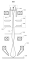
- Figure 2 shows an example of the configuration of the charged particle beam device of Example 1.
- Figure 2 shows the basic configuration of the electron optical system of the SEM, extracting the configuration for focusing the electron beam, such as the electron gun and lenses, and omits other structures, such as the deflector and aberration corrector.
- the electron gun 100 extracts electrons from the electron source 101 and emits them as an electron beam 110.
- electrons are extracted from the electron source.
- the extracted electrons are accelerated by the acceleration electrode 104 and emitted as the electron beam 110.
- An anode electrode 103 may be provided between the extraction electrode 102 and the acceleration electrode 104.
- the spread of the electron beam 110 emitted from the electron gun 100 can be controlled.
- an example in which the anode electrode 103 is provided in one stage is shown, but multiple stages of anode electrodes may be provided.
- the electron beam emitted from the electron gun 100 is controlled to be focused on the sample 109 by the first condenser lens 105, the second condenser lens 107, and the objective lens 108.
- the first condenser lens 105 which is usually (non-magnetic field superimposed) placed closer to the sample side than the electron gun 100, is placed directly below the electron source 101.
- the electron gun 100 is provided with a cylindrical electrode 301 directly below the electron source 101.
- the cylindrical electrode 301 is fixed to the extraction electrode 102, and the cylindrical electrode 301 and the extraction electrode 102 are at the same potential.
- the cylindrical electrode 301 and the first condenser lens 105 are in a positional relationship such that the main surface of the first condenser lens 105 crosses the cylindrical electrode 301.
- the electrostatic lens formed by the electrode group of the electron gun 100 and the magnetic lens of the first condenser lens 105 do not overlap spatially.
- the configuration of the electron gun 100 will be described in more detail later.
- the first condenser lens 105, the second condenser lens 107, and the objective lens 108 are magnetic field lenses.
- the coil is covered with a magnetic material that serves as a magnetic path, and a gap is provided in part of the magnetic path.
- a convex lens that bends electrons is formed as a result of the magnetic field leaking from the gap in the magnetic path. Therefore, the main surface of the magnetic field lens is formed at the position of the gap in the magnetic path.
- magnétique lenses which change the electron trajectory using a magnetic field generated by passing a current through a coil, which change the electron trajectory using an electric field between electrodes
- magnetic lenses do not require high voltage even when significantly changing the electron trajectory. For this reason, magnetic lenses are used for condenser lenses and objective lenses.
- the amount of current in the electron beam 110 is adjusted by adjusting the strength of the convex lenses of these magnetic lenses to control the amount of electrons passing through the aperture 106.
- the components of the electron gun 100 are described in detail below.
- the electron source 101 There are no particular limitations on the electron source 101. From the perspective of achieving high resolution, a Schottky electron source or a field emission electron source that uses an electric field to emit electrons is suitable.
- the electrode to which the cylindrical electrode 301 is fixed is not limited to the extraction electrode 102 shown in FIG. 2.
- the electrode to which the cylindrical electrode 301 is fixed must be an electrode located below the electron source 101.
- a suppressor electrode is provided at a position closer to the electron source 101 than the extraction electrode 102.
- the suppressor electrode is an electrode provided to suppress the electrons emitted from the side of the Schottky electron source from being emitted to the outside, and the suppressor electrode covers the side of the electron source, while the tip of the electron source protrudes from an opening provided in the electrode.
- the lower side of the electron source means the lower side (sample side) of the tip of the electron beam
- the suppressor electrode is not an electrode to which the cylindrical electrode 301 is fixed.
- the cylindrical electrode 301 may be fixed to an electrode (anode electrode) downstream of the extraction electrode 102 due to the electrode structure of the electron gun 100, etc.
- the cylindrical electrode 301 and the first condenser lens 105 are positioned such that the main surface of the first condenser lens 105 crosses the cylindrical electrode 301, when the cylindrical electrode 301 is fixed to the extraction electrode 102, it is possible to bring the main surface of the first condenser lens 105 closest to the electron source 101.
- the cylindrical electrode 301 will be described as being provided relative to the extraction electrode 102.
- the cylindrical electrode 301 is assembled so as to be suspended from the extraction electrode 102.
- the cylindrical electrode 301 has a cylindrical shape, and the length of the tube is preferably about 1 to 5 cm. It is also preferable that the diameter can be made wider. This has the effect of relaxing the precision of aligning the central axis of the cylindrical electrode 301 with the central axis of the extraction electrode 102, and relaxing the electric field strength generated at the tip of the cylindrical electrode 301.
- the axis alignment with the anode electrode 103 and the acceleration electrode 104 can also be performed by integrating the extraction electrode 102 and the cylindrical electrode 301.
- the central axes of the aligned extraction electrode 102, cylindrical electrode 301, anode electrode 103, and acceleration electrode 104 are the optical axis of the electrostatic lens formed by the group of electrodes included in the electron gun 100.
- the space inside the cylinder formed by the cylindrical electrode 301 and the main surface of the magnetic lens 105 are arranged so as to overlap.
- the main aberrations are spherical aberration and chromatic aberration, and the spread of electrons due to spherical aberration can be expressed as (1/4)Cs ⁇ 3 , and the spread of electrons due to chromatic aberration can be expressed as (1/2)Cc ⁇ ( ⁇ E/E).
- ⁇ is the convergence angle of the electron beam
- E is the energy of the electrons
- ⁇ E is the variation in the energy of the electrons, which are determined by the magnification of the electron source and the optical system.
- Cs and Cc are called the spherical aberration coefficient and the chromatic aberration coefficient, respectively, and indicate the characteristics of the lens.
- the magnetic field superposition allows the electron beam to pass through the magnetic lens with a small aberration coefficient.
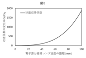
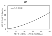
- Figures 3 and 4 show the relationship between the distance between the tip of the electron source and the main surface of the magnetic lens and the aberration coefficient obtained by simulation.
- the horizontal axis is the distance between the tip of the electron source 101 and the main surface of the magnetic lens 105 when the distance is set to 0.
- the vertical axis is the rate of change obtained by dividing the aberration coefficient that changes depending on the distance between the electron source and the main surface of the magnetic lens by the aberration coefficient C0 when the distance is 0. That is, the vertical axis of FIG. 3 is the rate of change Cs/ Cs0 of the spherical aberration coefficient, and the vertical axis of FIG. 4 is the rate of change Cc/ Cc0 of the chromatic aberration coefficient. It can be seen that the aberration coefficients of both spherical aberration and chromatic aberration increase sharply as the distance between the tip of the electron source and the main surface of the magnetic lens increases.
- the change in the aberration coefficient becomes gentle. From FIG. 3 and FIG. 4, for example, if the distance between the tip of the electron source and the main surface of the magnetic lens is 25 mm or less, the effect of suppressing the increase in the aberration of spherical aberration and chromatic aberration can be obtained.
- Additional work such as drilling holes may be performed on the side of the cylindrical electrode 301.
- the method of assembling the cylindrical electrode 301 to the electrode to which it is fixed is free, and it is sufficient to fix them by cutting threads in the area where the sides of both electrodes overlap and screwing them in place, or by welding or other methods.
- the extraction electrode 102 and the cylindrical electrode 301 are fixed in contact with each other, so they are always at the same potential. This means that if noise or disturbance due to the power supply occurs in the extraction electrode 102, noise or disturbance will also occur in the cylindrical electrode 301 in synchronization. Therefore, the space inside the cylindrical electrode 301 connected to the extraction electrode 102 becomes an equipotential space, and electrons emitted from the extraction electrode 102 travel through this equipotential space.
- the equipotential space formed by the cylindrical electrode 301 includes the optical axis of the electron gun 100, and no electric field is applied in the direction of electron travel. Therefore, the equipotential space is not affected by the electrostatic lens formed by the electrode group of the electron gun 100. By configuring the magnetic lens to act in the equipotential space, the electrostatic lens and the magnetic lens are spatially separated. This allows the axis adjustment of the electrostatic lens and the magnetic lens to be performed independently, just like in the case of non-overlapping magnetic fields.
- the method of forming the equipotential space is not limited to the cylindrical electrode 301, as long as it is equipotential in the direction of electron travel from the electron source 101.
- an equipotential plate electrode in the direction of electron travel.
- many other electrodes and deflectors are arranged within the charged particle beam device, there is a high possibility of receiving various noises, and therefore it is preferable from the standpoint of noise resistance to form the equipotential space inside a cylindrical electrode that has side walls of a specified length along the optical axis.
- the material of the cylindrical electrode 301 is a non-magnetic metal such as SUS or phosphor bronze.
- the material of the electrode to which the cylindrical electrode 301 is fixed in this case the extraction electrode 102, is a magnetic material such as permalloy or permendur. This allows the electrode to which the cylindrical electrode 301 is fixed to function as a magnetic field shield, making it possible to reduce the distance between the electron source 101 and the first condenser lens 105 while suppressing leakage of the magnetic field from the magnetic field lens 105.
- the magnetic lens acts on the electrons emitted into the equipotential space in the cylindrical electrode 301, and the sensitivity of the electrons focused by the magnetic lens is determined by the energy of the electrons emitted into the equipotential space, and in the configuration of FIG. 2, the condition of the extraction electrode 102, and is not affected by the conditions of the anode electrode 103 and the acceleration electrode 104 located below the cylindrical electrode 301.
- the strength of the magnetic lens that focuses the electrons in the equipotential space does not change whether the electron gun 100 emits an electron beam under high acceleration conditions or low acceleration conditions. Therefore, the first condenser lens 105 can be a magnetic lens of a small coil with a relatively small excitation current.
- the temperature rise due to the heat generated by the coil due to the excitation current is suppressed to about 10°C, and does not significantly exceed the room temperature, so that the performance fluctuation of the magnetic lens 105 due to the change in temperature over time can also be suppressed.
- FIG. 1 shows an example in which a magnetic lens having an extended magnetic path is used as the first condenser lens 105 shown in FIG. 2.
- the coil of the magnetic lens 105 is located at the same position as the lens main surface, that is, the cylindrical electrode 301. Therefore, a space for storing the coil is required near the electron source 101 at the top of the housing that houses the electron optical system.
- the structure around the electron source 101 becomes huge and the center of gravity of the housing moves upward, so that the structure is weak against vibration compared to a housing that houses an electron optical system with no magnetic field superimposed.
- Figure 5A shows an example in which a top lens type magnetic lens 501 that forms a lens above the coil is used as the first condenser lens 105. By positioning the coil further downward, the main surface of the lens can be brought closer to the electron source 101 while maintaining the center of gravity downward.
- the example of Figure 5A is not limited to this, and the positional relationship with the acceleration electrode 104 and other components can also be changed.
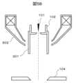
- FIG. 5B shows an example in which a bottom lens type magnetic field lens 502 that forms a lens below the coil is applied as the first condenser lens 105.
- the electrodes of the electron gun 100 are densely arranged, making it difficult to store a coil, whereas it is easier to secure space to store a coil above the electron source. For the same reason, it is also easy to add an axis adjustment mechanism above the electron source. As the center of gravity moves upward as mentioned above, measures against vibration can be taken, for example, by erecting vibration-damping supports.
- magnetic field lenses may contain resin in the coil portion, so it is undesirable to expose them to temperatures above 200°C.
- the area around the electron source is baked to high temperatures to increase the degree of vacuum, and in some places the temperature can reach around 300°C. For this reason, by increasing the distance between the main surface of the magnetic field lens and the coil, as in this modified example, the effects of baking the electron source can be avoided.
- the position of the coil of the magnetic field lens of the first condenser lens 105 can be selected at any location, thereby avoiding design risks.
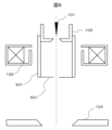
- (Variation 2) 6 shows an example of a second modification in which a differential exhaust aperture 601 is provided on the cylindrical electrode 301.
- the degree of vacuum in the space directly below the extraction electrode 102 is equal to that in the space around the acceleration electrode 104.
- the differential exhaust aperture 601 serves the function of differential exhaust to reduce the conductance of exhaust from the cylindrical electrode 301 to the acceleration electrode 104 side, thereby making it possible to maintain a high degree of vacuum. In addition, it is also possible to prevent gas adsorption to the electron source 101 by shielding gas molecules blowing up from below.
- the material of the differential exhaust aperture 601 is a non-magnetic metal such as SUS or phosphor bronze.
- the cylindrical electrode 301 forms an equipotential space immediately below the electron source 101, which is equipotential with the electrode to which the cylindrical electrode 301 is fixed (for example, the extraction electrode 102 in the example of FIG. 2).
- the distance over which electrons are accelerated from the extraction electrode 102 to the acceleration electrode 104 is shortened by the insertion of the cylindrical electrode 301.
- This means that a strong electrostatic lens is generated due to the increase in the gradient of the electric field between the cylindrical electrode 301 and the acceleration electrode 104.
- the trajectory of the electrons may be bent and focused at an angle greater than necessary at the end of the electrostatic lens, i.e., near the opening side wall of the cylindrical electrode 301 on the acceleration electrode 104 side.
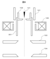
- the cylindrical electrode is modified from a simple cylindrical shape.
- the cylindrical electrode 701 shown in Figure 7 has a convex shape with a larger diameter near the opening on the acceleration electrode 104 side.
- the opening of the cylindrical electrode 701 on the acceleration electrode 104 side is made as large as possible, the focusing force of the electrostatic lens can be alleviated.
- Figure 7 shows an example in which the diameter of the cylindrical electrode increases in two stages in the optical axis direction, but the diameter may be increased in stages over three or more stages, or the diameter of the cylindrical electrode may be increased continuously.
- the strength of the electrostatic lens generated near the opening of the cylindrical electrode can be reduced by increasing the diameter of the opening on the acceleration electrode 104 side of the cylindrical electrode.
- (Variation 4) 8 shows an example of a fourth modification in which a magnetic field shield 121 is provided on the electron gun 100.
- the electrode the extraction electrode 102 in the example of FIG. 2 to which the cylindrical electrode 301 is fixed is made of a magnetic material so that the magnetic field from the magnetic field lens 105 does not leak to the electron source 101. In this case, there is a risk that a magnetic field lens will be formed due to the magnetic field concentrating at the opening of the extraction electrode 102.
- the material of the extraction electrode 102 is non-magnetic, and a magnetic field shield 121 is provided around the outer periphery of the extraction electrode 102.
- the magnetic field shield 121 is made of a magnetic material, and is positioned so as to hide the sidewall of the extraction electrode 102 from the magnetic field lens.
- the cylindrical magnetic field shield 121 is installed at the same height as the extraction electrode 102. It is preferable that the lower end of the magnetic field shield 121 reach a position that covers the area where the extraction electrode 102 and the cylindrical electrode 301 overlap.
- the magnetic field shield can suppress the generation of a magnetic field lens at the electrode opening where the cylindrical electrode is fixed, and prevent the magnetic field from leaking to the electron source.
- the cylindrical electrode 301 and an electrode located below the electron source are fixed and electrically connected to be at the same potential.
- the electrostatic lens directly below the cylindrical electrode 301 will be strong.
- a constant potential difference is given to the potential of the equipotential space with respect to the potential of the extraction electrode 102.
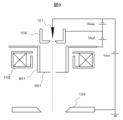
- Figure 9 shows an example of the power supply configuration in the electron gun of the second embodiment. As shown in Figure 9, a buffer potential Vbuf is applied to the cylindrical electrode 801, based on the potential Vbias of the extraction electrode 102.
- the cylindrical electrode 801 by making the cylindrical electrode 801 at a potential higher than the extraction electrode 102 by the buffer potential Vbuf, the potential difference between the cylindrical electrode 801 and the acceleration electrode 104 to which the potential Vacc is applied is smaller than in the configuration of the first embodiment, and the strength of the electrostatic lens directly below the cylindrical electrode 801 can be mitigated.
- a differential exhaust aperture 601 is provided as in Modification Example 2, a configuration in which a differential exhaust aperture 601 is not provided is also possible.
- the cylindrical electrode 801 is given a buffer potential Vbuf based on the potential Vbias of the extraction electrode 102, even if the observation conditions such as the acceleration voltage Vacc and extraction voltage Vbias are changed after the potential Vbuf is set, the potential difference between the extraction electrode 102 and the cylindrical electrode 801 is maintained at the buffer potential Vbuf regardless of the observation conditions.
- the potential difference between the cylindrical electrode and the acceleration electrode can be made smaller than in the first embodiment, and the strength of the electrostatic lens directly below the cylindrical electrode 801 can be reduced.
- Example 3 relates to an axial adjustment mechanism.
- the electrode structure may be either that of Example 1 or Example 2.
- Example 1 an example was described in which the cylindrical electrode 301 is assembled so as to be suspended from the extraction electrode 102. In this case, axial adjustment between the extraction electrode 102 and the cylindrical electrode 301 is impossible after assembly, and the potential of the equipotential space is inevitably the potential of the extraction electrode 102.
- the axial adjustment unit configuration shown below axial adjustment between the extraction electrode 102 and the cylindrical electrode 301 is possible after assembly, and the potential of the equipotential space as shown in Example 2 can be made different from the potential of the extraction electrode 102.
- FIG. 10 shows the configuration of an electron gun including an axial adjustment unit in the case of the electrode structure of Example 1.
- the first electrode 901 is, for example, an extraction electrode
- the second electrode 902 is a cylindrical electrode.
- a stopper 905 that supports the first electrode 901 is provided on the inner wall of the second electrode 902.
- a differential exhaust aperture 601 is provided at the opening of the second electrode 902.
- the electron source 101, the first electrode 901, and the second electrode 902 are integrated as an axial adjustment unit.
- the first electrode 901 and the second electrode 902 are attached to the electron source 101 in this order, upside down from the state when mounted on the charged particle beam device.
- fixing screws 904 are passed through drilled holes provided on both electrodes and fixed to the housing.
- the drilled hole 906 provided on the second electrode 902 is a drilled hole with a margin so that the second electrode 902 can be moved horizontally.
- a screw hole is provided in the side wall of the second electrode 902 (the side wall above the stopper 905 when mounted in the charged particle beam device).
- the axial adjustment screw 903 is passed through the screw hole of the second electrode 902, and the tip of the axial adjustment screw 903 is in contact with the first electrode 901.
- a temporary assembly is performed without tightening the screws, and then the position of the second electrode 902 relative to the first electrode 901 is moved by pushing the axial adjustment screw 903 toward the first electrode 901 (axial adjustment).
- the electron source 101, first electrode 901, second electrode 902, and differential exhaust aperture 601 can be axially adjusted by tightening the fixing screw 904. This unit is combined with the magnetic field lens 105, acceleration electrode 104, etc.
- an insulator is provided between the first electrode 901 and the second electrode 902 to prevent the first electrode 901 and the second electrode 902 from contacting each other, thereby preventing electrical contact between the two.
- the electron source 101, the first electrode 901, and the second electrode 902 can be integrated as an axis adjustment unit.
- the use of SEM has been exemplified by the inspection of semiconductor devices, similar issues arise in analytical applications used in universities and research facilities.
- the variety of samples increases more than in the inspection of semiconductor devices, such as in the observation of living organisms.
- the present disclosure is useful for charged particle beam devices in general that are equipped with a charged particle optical system that includes a charged particle gun including an electron source and a magnetic field lens.
- 101 electron source
- 102 extraction electrode
- 103 anode electrode
- 104 acceleration electrode
- 105 magnetic lens (first condenser lens)
- 106 aperture
- 107 magnetic lens (second condenser lens)
- 108 objective lens
- 109 sample
- 110 electron beam (small current)
- 111 electron beam (large current)
- 112 principal surface position (when magnetic field is not superimposed)
- 113 principal surface position (when magnetic field is superimposed)
- 121 magnetic field shield
- 301 701, 801: cylindrical electrodes
- 501 top lens type magnetic lens
- 502 bottom lens type magnetic lens
- 601 differential exhaust aperture
- 901 first electrode
- 902 second electrode
- 903 axis adjustment screw
- 904 fixing screw
- 905 stopper
- 906 drill hole.
Landscapes
- Chemical & Material Sciences (AREA)
- Analytical Chemistry (AREA)
- Physics & Mathematics (AREA)
- Electromagnetism (AREA)
- Electron Beam Exposure (AREA)
- Electron Sources, Ion Sources (AREA)
Abstract
Description
図5Aおよび図5Bに、図2に示した第1コンデンサレンズ105として、磁路を伸ばした形状をもつ磁場レンズを採用する例を示す。図2の構成では、磁場レンズ105のコイルの位置がレンズ主面と同じ筒状電極301の位置にある。このため、電子光学系を収容する筐体の最上部にある電子源101付近にコイルを収納するスペースが必要となる。これにより、電子源101周辺の構造が巨大化して筐体の重心も上方に移動するため、磁界非重畳の電子光学系を収容する筐体に比べると、振動に対して弱い構造といえる。
図6に変形例2として、筒状電極301に差動排気絞り601を設ける例を示す。図2のように、筒状電極301が単純な筒形状である場合には、引出電極102直下の空間の真空度は加速電極104周辺の空間と同等となる。しかしながら、電子源101に近く、低エネルギーの電子が通過する空間である引出電極102から筒状電極301までの間は高真空であることが望ましい。そこで、変形例2のように、筒状電極301の開口部に径の小さな差動排気絞り601を装着する。差動排気絞り601は筒状電極301から加速電極104側に排気するコンダクタンスを小さくする差動排気の機能を果たすことにより、高い真空度を維持することができる。また、下方から吹き上がるガス分子を遮蔽して、電子源101のガス吸着を防ぐこともできる。差動排気絞り601の材料は、SUSやリン青銅などの非磁性体の金属とする。
筒状電極301は、筒状電極301が固定された電極(例えば、図2の例であれば引出電極102)と等電位である等電位空間を電子源101直下に形成する。これにより、筒状電極301の挿入分だけ、引出電極102から加速電極104までの電子を加速させる距離が短くなる。このことは筒状電極301と加速電極104との間の電界の勾配が大きくなることにより、強い静電レンズが発生することを意味する。このため、高加速条件で電子ビームを放出させる場合、この静電レンズを制御できないリスクがある。例えば、静電レンズの端部、すなわち筒状電極301の加速電極104側の開口側壁付近で必要以上の角度で電子の軌道が曲げられ、集束する場合がある。
図8に変形例4として、電子銃100に磁場シールド121を設ける例を示す。実施例1では、電子源101に磁場レンズ105からの磁場が漏れないよう、筒状電極301が固定される電極(図2の例では引出電極102)を磁性体とする例を示した。この場合、引出電極102の開口部に磁場が集まることにより磁場レンズが形成されるリスクがある。
Claims (13)
- 荷電粒子源を備える荷電粒子銃と、
前記荷電粒子銃からの荷電粒子ビームをサンプル上に集束させる荷電粒子光学系と、を有し、
前記荷電粒子銃は、前記荷電粒子源の下側に位置する第1電極及び前記第1電極の下側に位置する加速電極を備え、前記第1電極と前記加速電極との間に、光軸を含んで、前記荷電粒子源からの荷電粒子の進行方向において前記第1電極の電位と等電位である、または前記第1電極の電位に対して一定の電位差をもつ等電位空間が形成されており、
前記荷電粒子光学系は、その主面が前記等電位空間を横切るように配置される磁場レンズを備える荷電粒子線装置。 - 請求項1において、
前記第1電極は、前記荷電粒子源から荷電粒子を引き出す引出電極であり、
前記等電位空間は、光軸方向に延びる側壁をもつ筒状電極の内部に形成される荷電粒子線装置。 - 請求項2において、
前記引出電極の材料は磁性体であり、前記筒状電極の材料は非磁性体である荷電粒子線装置。 - 請求項2において、
前記筒状電極は前記引出電極と電気的に接続されている荷電粒子線装置。 - 請求項2において、
前記筒状電極に前記引出電極の電位を基準として所定の緩衝電位が印加される荷電粒子線装置。 - 請求項1において、
前記磁場レンズは、前記主面よりも低い位置にコイルを備えるトップレンズ型磁場レンズ、または前記主面よりも高い位置にコイルを備えるボトムレンズ型磁場レンズである荷電粒子線装置。 - 請求項2において、
前記筒状電極は、前記加速電極側の開口部において差動排気絞りを備える荷電粒子線装置。 - 請求項2において、
前記筒状電極は、前記加速電極側の開口部において径が大きくされている荷電粒子線装置。 - 請求項2において、
前記荷電粒子銃は、前記引出電極の外周を囲う磁場シールドを備え、
前記磁場シールドの下端は、前記引出電極と前記筒状電極とが重なる箇所を覆う高さとする荷電粒子線装置。 - 荷電粒子源を備える荷電粒子銃と、
前記荷電粒子銃からの荷電粒子ビームをサンプル上に集束させる荷電粒子光学系と、を有し、
前記荷電粒子銃は、前記荷電粒子源、第1電極及び第2電極を一体化した軸調ユニットと加速電極とを含み、
前記第2電極の円筒形状の内壁にストッパーが設けられており、前記ストッパー上に前記第1電極が支持され、
前記第2電極の前記ストッパーよりも上側の側壁に設けられたネジ穴を通して軸調ネジが前記第1電極に接触するように設けられ、
前記荷電粒子光学系は、その主面が前記ストッパーよりも下の位置で前記第2電極を横切るように配置される磁場レンズを備える荷電粒子線装置。 - 請求項10において、
前記第1電極と前記第2電極とは電気的に接続されている、または前記第1電極と前記第2電極とは電気的に絶縁され、前記第2電極に前記第1電極の電位を基準として所定の緩衝電位が印加される荷電粒子線装置。 - 請求項10において、
前記第1電極は、前記荷電粒子源から荷電粒子を引き出す引出電極である荷電粒子線装置。 - 請求項10において、
前記第1電極の材料は磁性体であり、前記第2電極の材料は非磁性体である荷電粒子線装置。
Priority Applications (5)
| Application Number | Priority Date | Filing Date | Title |
|---|---|---|---|
| US19/150,591 US20260229443A1 (en) | 2023-03-29 | 2023-03-29 | Charged Particle Beam Device |
| PCT/JP2023/012891 WO2024201811A1 (ja) | 2023-03-29 | 2023-03-29 | 荷電粒子線装置 |
| KR1020257022939A KR20250120403A (ko) | 2023-03-29 | 2023-03-29 | 하전 입자선 장치 |
| CN202380092086.2A CN120513502A (zh) | 2023-03-29 | 2023-03-29 | 带电粒子束装置 |
| TW113111377A TWI917910B (zh) | 2023-03-29 | 2024-03-27 | 帶電粒子線裝置 |
Applications Claiming Priority (1)
| Application Number | Priority Date | Filing Date | Title |
|---|---|---|---|
| PCT/JP2023/012891 WO2024201811A1 (ja) | 2023-03-29 | 2023-03-29 | 荷電粒子線装置 |
Publications (1)
| Publication Number | Publication Date |
|---|---|
| WO2024201811A1 true WO2024201811A1 (ja) | 2024-10-03 |
Family
ID=92903632
Family Applications (1)
| Application Number | Title | Priority Date | Filing Date |
|---|---|---|---|
| PCT/JP2023/012891 Ceased WO2024201811A1 (ja) | 2023-03-29 | 2023-03-29 | 荷電粒子線装置 |
Country Status (5)
| Country | Link |
|---|---|
| US (1) | US20260229443A1 (ja) |
| KR (1) | KR20250120403A (ja) |
| CN (1) | CN120513502A (ja) |
| TW (1) | TWI917910B (ja) |
| WO (1) | WO2024201811A1 (ja) |
Cited By (1)
| Publication number | Priority date | Publication date | Assignee | Title |
|---|---|---|---|---|
| CZ310701B6 (cs) * | 2024-11-25 | 2026-05-13 | Tescan Group, A.S. | Kombinovaná elektrostaticko-magnetická objektivová čočka |
Citations (1)
| Publication number | Priority date | Publication date | Assignee | Title |
|---|---|---|---|---|
| JP2013225521A (ja) * | 2013-06-17 | 2013-10-31 | Hitachi High-Technologies Corp | 電子銃 |
Family Cites Families (7)
| Publication number | Priority date | Publication date | Assignee | Title |
|---|---|---|---|---|
| US9799484B2 (en) | 2014-12-09 | 2017-10-24 | Hermes Microvision, Inc. | Charged particle source |
| JP6177817B2 (ja) | 2015-01-30 | 2017-08-09 | 松定プレシジョン株式会社 | 荷電粒子線装置及び走査電子顕微鏡 |
| JP2019003863A (ja) | 2017-06-16 | 2019-01-10 | 株式会社島津製作所 | 電子ビーム装置、ならびに、これを備えるx線発生装置および走査電子顕微鏡 |
| US11211224B2 (en) | 2018-04-26 | 2021-12-28 | Hitachi High-Tech Corporation | Charged particle beam apparatus |
| EP3953960A1 (en) | 2019-04-10 | 2022-02-16 | ASML Netherlands B.V. | Stage apparatus suitable for a particle beam apparatus |
| JP6722958B1 (ja) | 2019-11-20 | 2020-07-15 | 株式会社Photo electron Soul | 電子線適用装置および電子線適用装置における電子ビームの射出方法 |
| US11636996B2 (en) | 2020-09-09 | 2023-04-25 | Kla Corporation | Magnetic immersion electron gun |
-
2023
- 2023-03-29 US US19/150,591 patent/US20260229443A1/en active Pending
- 2023-03-29 WO PCT/JP2023/012891 patent/WO2024201811A1/ja not_active Ceased
- 2023-03-29 CN CN202380092086.2A patent/CN120513502A/zh active Pending
- 2023-03-29 KR KR1020257022939A patent/KR20250120403A/ko active Pending
-
2024
- 2024-03-27 TW TW113111377A patent/TWI917910B/zh active
Patent Citations (1)
| Publication number | Priority date | Publication date | Assignee | Title |
|---|---|---|---|---|
| JP2013225521A (ja) * | 2013-06-17 | 2013-10-31 | Hitachi High-Technologies Corp | 電子銃 |
Cited By (1)
| Publication number | Priority date | Publication date | Assignee | Title |
|---|---|---|---|---|
| CZ310701B6 (cs) * | 2024-11-25 | 2026-05-13 | Tescan Group, A.S. | Kombinovaná elektrostaticko-magnetická objektivová čočka |
Also Published As
| Publication number | Publication date |
|---|---|
| CN120513502A (zh) | 2025-08-19 |
| TWI917910B (zh) | 2026-03-11 |
| TW202439358A (zh) | 2024-10-01 |
| US20260229443A1 (en) | 2026-08-06 |
| KR20250120403A (ko) | 2025-08-08 |
Similar Documents
| Publication | Publication Date | Title |
|---|---|---|
| US12027342B2 (en) | Charged particle beam device and axis adjustment method thereof | |
| US6191423B1 (en) | Correction device for correcting the spherical aberration in particle-optical apparatus | |
| TWI435362B (zh) | 帶電粒子裝置 | |
| TWI749396B (zh) | 電磁複合透鏡、帶電粒子光學系統、及用以組態具有光軸之電磁複合透鏡之方法 | |
| JP2020102452A (ja) | 荷電粒子ビーム装置、荷電粒子ビーム装置のための交換可能マルチ開孔構成、および荷電粒子ビーム装置を操作するための方法 | |
| CN1406391A (zh) | 带电粒子束设备的光学柱 | |
| JP6404736B2 (ja) | 複合荷電粒子線装置 | |
| JP6389569B2 (ja) | モノクロメーターおよびこれを備えた荷電粒子線装置 | |
| JPWO2018179115A1 (ja) | 荷電粒子線装置 | |
| WO2011055520A1 (ja) | 電子顕微鏡 | |
| US7326927B2 (en) | Focusing lens and charged particle beam device for titled landing angle operation | |
| US7652263B2 (en) | Focussing lens for charged particle beams | |
| TWI917910B (zh) | 帶電粒子線裝置 | |
| JP2006324119A (ja) | 電子銃 | |
| WO2014069271A1 (ja) | 荷電粒子線装置 | |
| EP0079931A4 (en) | FOCUSED ION RAY MICROMAKING PILLAR. | |
| JP2019075392A (ja) | 荷電粒子線装置 | |
| JP7751929B1 (ja) | 荷電粒子銃 | |
| KR102821024B1 (ko) | 대물 렌즈 및 이를 포함하는 하전 입자선 장치 | |
| CN120126987A (zh) | 物镜、包括该物镜的带电粒子显微镜以及相关方法 |
Legal Events
| Date | Code | Title | Description |
|---|---|---|---|
| 121 | Ep: the epo has been informed by wipo that ep was designated in this application |
Ref document number: 23930449 Country of ref document: EP Kind code of ref document: A1 |
|
| ENP | Entry into the national phase |
Ref document number: 1020257022939 Country of ref document: KR Free format text: ST27 STATUS EVENT CODE: A-0-1-A10-A15-NAP-PA0105 (AS PROVIDED BY THE NATIONAL OFFICE) |
|
| WWE | Wipo information: entry into national phase |
Ref document number: 1020257022939 Country of ref document: KR |
|
| WWE | Wipo information: entry into national phase |
Ref document number: 202380092086.2 Country of ref document: CN |
|
| WWP | Wipo information: published in national office |
Ref document number: 1020257022939 Country of ref document: KR |
|
| WWP | Wipo information: published in national office |
Ref document number: 202380092086.2 Country of ref document: CN |
|
| NENP | Non-entry into the national phase |
Ref country code: DE |
|
| 122 | Ep: pct application non-entry in european phase |
Ref document number: 23930449 Country of ref document: EP Kind code of ref document: A1 |
|
| NENP | Non-entry into the national phase |
Ref country code: JP |