WO2024201729A1 - 表示装置 - Google Patents
表示装置 Download PDFInfo
- Publication number
- WO2024201729A1 WO2024201729A1 PCT/JP2023/012590 JP2023012590W WO2024201729A1 WO 2024201729 A1 WO2024201729 A1 WO 2024201729A1 JP 2023012590 W JP2023012590 W JP 2023012590W WO 2024201729 A1 WO2024201729 A1 WO 2024201729A1
- Authority
- WO
- WIPO (PCT)
- Prior art keywords
- light
- layer
- resonator length
- distance
- emitting layer
- Prior art date
- Legal status (The legal status is an assumption and is not a legal conclusion. Google has not performed a legal analysis and makes no representation as to the accuracy of the status listed.)
- Ceased
Links
Images





Classifications
-
- H—ELECTRICITY
- H05—ELECTRIC TECHNIQUES NOT OTHERWISE PROVIDED FOR
- H05B—ELECTRIC HEATING; ELECTRIC LIGHT SOURCES NOT OTHERWISE PROVIDED FOR; CIRCUIT ARRANGEMENTS FOR ELECTRIC LIGHT SOURCES, IN GENERAL
- H05B33/00—Electroluminescent light sources
- H05B33/12—Light sources with substantially two-dimensional [2D] radiating surfaces
-
- H—ELECTRICITY
- H05—ELECTRIC TECHNIQUES NOT OTHERWISE PROVIDED FOR
- H05B—ELECTRIC HEATING; ELECTRIC LIGHT SOURCES NOT OTHERWISE PROVIDED FOR; CIRCUIT ARRANGEMENTS FOR ELECTRIC LIGHT SOURCES, IN GENERAL
- H05B33/00—Electroluminescent light sources
- H05B33/12—Light sources with substantially two-dimensional [2D] radiating surfaces
- H05B33/14—Light sources with substantially two-dimensional [2D] radiating surfaces characterised by the chemical or physical composition or the arrangement of the electroluminescent material, or by the simultaneous addition of the electroluminescent material in or onto the light source
-
- H—ELECTRICITY
- H05—ELECTRIC TECHNIQUES NOT OTHERWISE PROVIDED FOR
- H05B—ELECTRIC HEATING; ELECTRIC LIGHT SOURCES NOT OTHERWISE PROVIDED FOR; CIRCUIT ARRANGEMENTS FOR ELECTRIC LIGHT SOURCES, IN GENERAL
- H05B33/00—Electroluminescent light sources
- H05B33/12—Light sources with substantially two-dimensional [2D] radiating surfaces
- H05B33/22—Light sources with substantially two-dimensional [2D] radiating surfaces characterised by the chemical or physical composition or the arrangement of auxiliary dielectric or reflective layers
- H05B33/24—Light sources with substantially two-dimensional [2D] radiating surfaces characterised by the chemical or physical composition or the arrangement of auxiliary dielectric or reflective layers of metallic reflective layers
-
- H—ELECTRICITY
- H10—SEMICONDUCTOR DEVICES; ELECTRIC SOLID-STATE DEVICES NOT OTHERWISE PROVIDED FOR
- H10K—ORGANIC ELECTRIC SOLID-STATE DEVICES
- H10K50/00—Organic light-emitting devices
- H10K50/10—OLEDs or polymer light-emitting diodes [PLED]
- H10K50/11—OLEDs or polymer light-emitting diodes [PLED] characterised by the electroluminescent [EL] layers
- H10K50/115—OLEDs or polymer light-emitting diodes [PLED] characterised by the electroluminescent [EL] layers comprising active inorganic nanostructures, e.g. luminescent quantum dots
-
- H—ELECTRICITY
- H10—SEMICONDUCTOR DEVICES; ELECTRIC SOLID-STATE DEVICES NOT OTHERWISE PROVIDED FOR
- H10K—ORGANIC ELECTRIC SOLID-STATE DEVICES
- H10K50/00—Organic light-emitting devices
- H10K50/80—Constructional details
-
- H—ELECTRICITY
- H10—SEMICONDUCTOR DEVICES; ELECTRIC SOLID-STATE DEVICES NOT OTHERWISE PROVIDED FOR
- H10K—ORGANIC ELECTRIC SOLID-STATE DEVICES
- H10K50/00—Organic light-emitting devices
- H10K50/80—Constructional details
- H10K50/805—Electrodes
- H10K50/82—Cathodes
- H10K50/826—Multilayers, e.g. opaque multilayers
-
- H—ELECTRICITY
- H10—SEMICONDUCTOR DEVICES; ELECTRIC SOLID-STATE DEVICES NOT OTHERWISE PROVIDED FOR
- H10K—ORGANIC ELECTRIC SOLID-STATE DEVICES
- H10K50/00—Organic light-emitting devices
- H10K50/80—Constructional details
- H10K50/85—Arrangements for extracting light from the devices
- H10K50/852—Arrangements for extracting light from the devices comprising a resonant cavity structure, e.g. Bragg reflector pair
-
- H—ELECTRICITY
- H10—SEMICONDUCTOR DEVICES; ELECTRIC SOLID-STATE DEVICES NOT OTHERWISE PROVIDED FOR
- H10K—ORGANIC ELECTRIC SOLID-STATE DEVICES
- H10K59/00—Integrated devices, or assemblies of multiple devices, comprising at least one organic light-emitting element covered by group H10K50/00
- H10K59/10—OLED displays
- H10K59/12—Active-matrix OLED [AMOLED] displays
- H10K59/122—Pixel-defining structures or layers, e.g. banks
-
- H—ELECTRICITY
- H10—SEMICONDUCTOR DEVICES; ELECTRIC SOLID-STATE DEVICES NOT OTHERWISE PROVIDED FOR
- H10K—ORGANIC ELECTRIC SOLID-STATE DEVICES
- H10K59/00—Integrated devices, or assemblies of multiple devices, comprising at least one organic light-emitting element covered by group H10K50/00
- H10K59/30—Devices specially adapted for multicolour light emission
- H10K59/35—Devices specially adapted for multicolour light emission comprising red-green-blue [RGB] subpixels
-
- H—ELECTRICITY
- H10—SEMICONDUCTOR DEVICES; ELECTRIC SOLID-STATE DEVICES NOT OTHERWISE PROVIDED FOR
- H10K—ORGANIC ELECTRIC SOLID-STATE DEVICES
- H10K2102/00—Constructional details relating to the organic devices covered by this subclass
- H10K2102/10—Transparent electrodes, e.g. using graphene
-
- H—ELECTRICITY
- H10—SEMICONDUCTOR DEVICES; ELECTRIC SOLID-STATE DEVICES NOT OTHERWISE PROVIDED FOR
- H10K—ORGANIC ELECTRIC SOLID-STATE DEVICES
- H10K2102/00—Constructional details relating to the organic devices covered by this subclass
- H10K2102/20—Metallic electrodes, e.g. using a stack of layers
Definitions
- This disclosure relates to a display device.
- Patent document 1 discloses an organic EL device in which multiple pixels correspond to red (R), green (G), and blue (B), the material of the organic functional layer that constitutes the organic EL element is the same regardless of the corresponding color, an optical resonator is formed in each pixel, and the optical length of the optical resonator is set to a length corresponding to either red light, green light, or blue light depending on the thickness of the light-emitting layer.
- Patent Document 1 sets the resonance length (cavity length) for each emitted color by controlling the thickness of the light-emitting layer, which creates the problem of reduced luminous efficiency of the light-emitting elements of one of the colors.
- the display device includes a red light-emitting element including a first light-reflecting layer, a first light-emitting layer, and a common electrode in this order, a green light-emitting element including a second light-reflecting layer, a second light-emitting layer, and a common electrode in this order, and a blue light-emitting element including a third light-reflecting layer, a third light-emitting layer, and a common electrode in this order, and is configured such that the first distance is the distance from the first light-reflecting layer to the common electrode, the second distance is the distance from the second light-reflecting layer to the common electrode, the third distance is the distance from the third light-reflecting layer to the common electrode, the fourth distance is the distance from the center surface of the first light-emitting layer to the first light-reflecting layer, the fifth distance is the distance from the center surface of the second light-emitting layer to the second light-reflecting layer, and the first distance is the distance from the
- the light-emitting efficiency of the light-emitting element can be improved.
- FIG. 1 is a plan view illustrating an example of a configuration of a display device according to an embodiment of the present disclosure.
- 1 is a cross-sectional view illustrating an example of a configuration of a display device according to an embodiment of the present disclosure.
- 1A and 1B are diagrams illustrating an optical resonator that can be formed in a light-emitting device.
- 1A and 1B are diagrams illustrating an optical resonator that can be formed in a light-emitting device.
- FIG. 11 is a cross-sectional view showing a modified example of the configuration of a display device according to an embodiment of the present disclosure.
- 1 is a cross-sectional view illustrating an example of a configuration of a display device according to an embodiment of the present disclosure.
- 7 is a partial cross-sectional view showing an example of the configuration of a first light-emitting layer shown in FIG. 6.
- 7 is a partial cross-sectional view showing an example of the configuration of the second light-emitting layer shown in FIG. 6.
- 7 is a partial cross-sectional view showing an example of the configuration of a third light-emitting layer shown in FIG. 6.
- 1 is a cross-sectional view illustrating an example of a configuration of a display device according to an embodiment of the present disclosure.
- Fig. 1 is a plan view showing an example of the configuration of a display device according to an embodiment of the present disclosure.
- the display device 100 includes a display section DA in which a plurality of pixels PX are provided, and a drive circuit DC for driving the display section DA.
- the plurality of pixels PX include a red pixel P1 including a red light-emitting element D1 and a pixel circuit E1, a green pixel P2 including a green light-emitting element D2 and a pixel circuit E2, and a blue pixel P3 including a blue light-emitting element D3 and a pixel circuit E3.
- attention will be paid to the red light-emitting element D1, the green light-emitting element D2, and the blue light-emitting element D3.
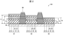
- the display device 100 includes a red light-emitting element D1 including a first light-reflecting layer A1, a first light-emitting layer B1, and a common electrode CE in this order, a green light-emitting element D2 including a second light-reflecting layer A2, a second light-emitting layer B2, and a common electrode CE in this order, and a blue light-emitting element D3 including a third light-reflecting layer A3, a third light-emitting layer B3, and a common electrode CE in this order, and the distance from the first light-reflecting layer A1 to the common electrode CE is a first distance f1, and the distance from the second light-reflecting layer A2 to the common electrode CE is a second distance f2.
- the distance at is the second distance f2
- the distance from the third light reflecting layer A3 to the common electrode CE is the third distance f3
- the distance from the center surface of the first light emitting layer B1 to the first light reflecting layer A1 is the fourth distance f4
- the distance from the center surface of the second light emitting layer B2 to the second light reflecting layer A2 is the fifth distance f5
- the distance from the center surface of the third light emitting layer B3 to the third light reflective layer A3 is the sixth distance f6, where first distance f1 > second distance f2 > third distance f3 and fourth distance f4 > fifth distance f5 > sixth distance f6.
- distance when used simply, it means geometric distance. When optical distance is intended, it is specified as “optical distance.” Similarly, “thickness” and “length” mean geometric thickness and geometric length, unless modified with “optical.” Distance, thickness, and length may be determined based on observation with a transmission electron microscope (TEM) or may be determined based on other methods such as ellipsometry.
- TEM transmission electron microscope
- central surface simply means the geometric central surface, i.e., the intermediate surface that is geometrically equidistant from the upper and lower surfaces.
- the surface with the highest brightness among the surfaces included in the light-emitting layer is referred to as the "light-emitting surface.”
- the first to third light-reflecting layers A1 to A3 may be light-reflecting electrodes or parts of light-reflecting electrodes, or light-reflecting films formed below the light-transmitting electrodes.
- the first to third light-reflecting layers A1 to A3 may be made of the same material and may be formed from the same layer.
- the first to third light-reflecting layers A1 to A3 may be made of silver (Ag), aluminum (Al), magnesium (Mg), or an alloy containing one or more of these.
- the common electrode CE has light-transmitting and light-reflective properties, and is located closer to the light extraction side than the first to third light-emitting layers B1 to B3.
- the common electrode CE may be made of a transparent metal oxide such as indium tin oxide (InTiO) and indium zinc oxide (InZnO).
- the red light-emitting element D1 includes a first light-transmitting layer G1 located between the first light-reflecting layer A1 and the first light-emitting layer B1
- the green light-emitting element D2 includes a second light-transmitting layer G2 located between the second light-reflecting layer A2 and the second light-emitting layer B2
- the blue light-emitting element D3 includes a third light-transmitting layer G3 located between the third light-reflecting layer A3 and the third light-emitting layer B3
- the thickness of the first light-transmitting layer G1 may be greater than the thickness of the second light-transmitting layer G2 and greater than the thickness of the third light-transmitting layer G3.
- the thickness of the first light-emitting layer B1 may be greater than the thickness of the second light-emitting layer B2 and greater than the thickness of the third light-emitting layer B3.
- the first to third light-emitting layers B1 to B3 may each contain an organic light-emitting material or quantum dots as the light-emitting material.
- the first to third light-emitting layers B1 to B3 may have substantially the same refractive index. In order to ensure good electrical characteristics of the red, green, and blue light-emitting elements D1 to D3, it is beneficial that the difference in thickness between the first light-emitting layer B1 and the third light-emitting layer B3 is 40 nm or less.
- Lower charge functional layers J1, J2, J3 of approximately the same thickness may be formed between the first light reflecting layer A1 and the first light emitting layer B1, between the second light reflecting layer A2 and the second light emitting layer B2, and between the third light reflecting layer A3 and the third light emitting layer B3.
- the lower charge functional layers J1, J2, J3 may be made of the same material and may be formed from the same layer.
- upper charge functional layers K1, K2, K3 of approximately the same thickness may be formed between the first light emitting layer B1 and the common electrode CE, between the second light emitting layer B2 and the common electrode CE, and between the third light emitting layer B3 and the common electrode CE.
- the upper charge functional layers K1, K2, K3 may be made of the same material and may be formed from the same layer.
- the thicknesses of the upper charge functional layers K1, K2, and K3 are measured at the center of each of the red, green, and blue light-emitting elements D1 to D3 in a plan view, and when the difference between the maximum and minimum thicknesses of the upper charge functional layers K1, K2, and K3 is 10 nm or less, the thicknesses of the upper charge functional layers K1, K2, and K3 may be considered to be the same.
- the layer above the common electrode CE may have a lower refractive index than the common electrode CE (e.g., the atmospheric layer).
- the display device 100 may include additional components (not shown) located above the first to third light-emitting layers B1 to B3, so long as the configuration of the layers above the first to third light-emitting layers B1 to B3 is common to the red, green, and blue light-emitting elements D1 to D3 in terms of material and layer thickness.
- the display device 100 may include other components as appropriate, such as a bank layer BH, a circuit board SB on which the red, green, and blue light-emitting elements D1 to D3 are formed, and a sealing layer (not shown) that covers the red, green, and blue light-emitting elements D1 to D3.
- the first light-emitting layer B1 may contain a light-emitting material other than a red light-emitting material.
- the second light-emitting layer B2 may contain a light-emitting material other than a green light-emitting material
- the third light-emitting layer B3 may contain a light-emitting material other than a blue light-emitting material.
- the first to third light-emitting layers B1 to B3 may contain the same light-emitting material group.
- the volume ratio of the red light-emitting material is the highest in the light-emitting material in the first light-emitting layer B1.
- the volume ratio of the green light-emitting material is the highest in the light-emitting material in the second light-emitting layer B2
- the volume ratio of the blue light-emitting material is the highest in the light-emitting material in the third light-emitting layer B3.
- the volume ratio of the light-emitting material may be determined from the area ratio. For example, if the first light-emitting layer B1 contains quantum dots as the light-emitting material, a cross section of the first light-emitting layer B1 is imaged with an electron microscope, the areas of the quantum dots in the image are measured, and the areas are added up for each light-emitting color. When the total area of the red-emitting quantum dots is the largest, it may be determined that the quantum dots with the highest volume ratio in the first light-emitting layer B1 are the red-emitting quantum dots.
- the common electrode CE may be a cathode, and the first light-reflecting layer A1, the second light-reflecting layer A2, and the third light-reflecting layer A3 may be anodes located below the common electrode CE. Additionally or alternatively, the common electrode CE may be a cathode, and the first light-transmitting layer G1, the second light-transmitting layer G2, and the third light-transmitting layer G3 may be anodes located below the common electrode CE. In the example shown in FIG.
- the first to third light-transmitting layers G1 to G3 are in contact with the first to third light-reflecting layers A1 to A3, respectively, and cooperate to form the first to third light-reflecting electrodes H1 to H3, and the first to third light-reflecting electrodes H1 to H3 are anodes, respectively.
- the first to third light-transmitting layers G1 to G3 may be separated from the first to third light-reflecting layers A1 to A3, respectively.
- the common electrode CE may be an anode, and each of the first to third light-reflecting layers A1 to A3 may be a cathode located below the common electrode CE. Additionally or alternatively, the common electrode CE may be an anode, and each of the first to third light-transmitting layers G1 to G3 may be a cathode located below the common electrode CE.
- the first to third light transmitting layers G1 to G3 may have substantially the same refractive index.
- the first to third light transmitting layers G1 to G3 may be made of the same material.
- the first light transmitting layer G1, the second light transmitting layer G2, and the third light transmitting layers G1 to G3 may each be made of a transparent metal oxide such as indium tin oxide (InTiO) and indium zinc oxide (InZnO).
- Optical resonator In the red light emitting element D1, one or more optical resonators in which the red light constructively interacts with each other may be formed.
- the wavelength of the red light is 600 to 770 nm.
- the first distance f1 may be an n-th order resonator length for the red light to constructively interact between the first light reflecting layer A1 and the common electrode CE, and at this time, an optical resonator in which the red light constructively interacts with each other is formed between the first light reflecting layer A1 and the common electrode CE.
- the distance from the light emitting surface of the first light emitting layer B1 to the first light reflecting layer A1 may be an n-th order resonator length for the red light to constructively interact between the light emitting surface of the first light emitting layer B1 and the first light reflecting layer A1, and at this time, an optical resonator in which the red light constructively interacts with each other is formed between the light emitting surface of the first light emitting layer B1 and the first light reflecting layer A1.
- the "n” in the "n-th order resonator length" is any natural number.
- Human visual sensitivity is highest in the vicinity of 555 [nm], that is, on the shorter wavelength side than red light.
- the above distances may be designed to be shorter than the n-th order resonator length.
- the light emitting surface of the first light emitting layer B1 may be replaced with the geometric center plane of the first light emitting layer B1.
- the first distance f1 may be equal to or less than the n-th order resonator length R 1,n , where R 1,n is the n-th order resonator length for the red light to reinforce each other between the first light reflecting layer A1 and the common electrode CE, and the difference between the first distance f1 and the n-th order resonator length R 1,n may be equal to or less than 20% of the difference between the (n-1)th order resonator length R 1,n-1 and the n-th order resonator length R 1,n .
- the difference is an absolute value. That is, the following inequality (1) may be satisfied.
- the zero-order resonator length R 1,0 is set to 0 [nm] regardless of the phase shift.
- the fourth distance f4 may be equal to or less than the n-th order resonator length R4 ,n, where R4,n is the n-th order resonator length for the red light to reinforce each other between the center surface of the first light emitting layer B1 and the first light reflecting layer A1, and the difference between the fourth distance f4 and the n-th order resonator length R4 ,n may be equal to or less than 20% of the difference between the (n-1)th order resonator length R4,n-1 and the n-th order resonator length R4 ,n .
- the difference is an absolute value. That is, the following inequality (2) may be satisfied.
- the 0th order resonator length R4,0 is set to 0 [nm] regardless of the phase shift.
- one or more optical resonators may be formed in which the green light reinforces each other.
- the wavelength of the green light is 490 to 550 nm.
- the second distance f2 may be an n-th order resonator length for the green light to reinforce each other between the second light reflecting layer A2 and the common electrode CE, and in this case, an optical resonator for the green light to reinforce each other is formed between the second light reflecting layer A2 and the common electrode CE.
- the distance from the light-emitting surface of the second light-emitting layer B2 to the second light reflecting layer A2 may be an n-th order resonator length for the green light to reinforce each other between the light-emitting surface of the second light-emitting layer B2 and the second light reflecting layer A2, and in this case, an optical resonator for the green light to reinforce each other is formed between the light-emitting surface of the second light-emitting layer B2 and the second light reflecting layer A2.
- the above distances may be designed to be longer than the n-th order resonator length.
- the light emitting surface of the second light emitting layer B2 may be replaced with the geometric center plane of the second light emitting layer B2.
- the second distance f2 may be greater than or equal to the n-th order resonator length R 2,n , where R 2,n is the n-th order resonator length for the green light to reinforce each other between the second light reflecting layer A2 and the common electrode CE, and the difference between the second distance f2 and the n-th order resonator length R 2 ,n may be 20% or less of the difference between the (n+1)th order resonator length R 2,n+1 and the n-th order resonator length R 2,n .
- the difference is an absolute value. That is, the following inequality (3) may be satisfied.
- the 0-th order resonator length R 2,0 is set to 0 [nm] regardless of the phase shift.
- the fifth distance f5 may be greater than or equal to the n-th order resonator length R5 ,n, where R5,n is the n-th order resonator length for the green light to reinforce each other between the center surface of the second light emitting layer B2 and the second light reflecting layer A2, and the difference between the fifth distance f5 and the n-th order resonator length R5 ,n may be less than or equal to 20% of the difference between the (n+1)th order resonator length R5,n+1 and the n-th order resonator length R5 ,n .
- the difference is an absolute value. That is, the following inequality (4) may be satisfied.
- the zeroth order resonator length R5,0 is set to 0 [nm] regardless of the phase shift.
- one or more optical resonators may be formed in which the blue light components are reinforced.
- the wavelength of the blue light is 430 to 490 nm.
- the third distance f3 may be an n-th order resonator length for the blue light components to reinforce each other between the third light reflecting layer A3 and the common electrode CE, and in this case, an optical resonator for the blue light components to reinforce each other is formed between the third light reflecting layer A3 and the common electrode CE.
- the distance from the light-emitting surface of the third light-emitting layer B3 to the third light reflecting layer A3 may be an n-th order resonator length for the blue light components to reinforce each other between the light-emitting surface of the third light-emitting layer B3 and the third light reflecting layer A3, and in this case, an optical resonator for the blue light components to reinforce each other is formed between the light-emitting surface of the third light-emitting layer B3 and the third light reflecting layer A3.
- the above distances may be designed to be longer than the n-th order resonator length.
- the light emitting surface of the third light emitting layer B3 may be replaced with the geometric center plane of the third light emitting layer B3.
- the third distance f3 may be greater than or equal to the n-th order resonator length R 3,n , where R 3,n is the n-th order resonator length for blue light to reinforce each other between the third light reflecting layer A3 and the common electrode CE, and the difference between the third distance f3 and the n-th order resonator length R 3,n may be 20% or less of the difference between the (n+1)th order resonator length R 3 ,n+1 and the n-th order resonator length R 3,n .
- the difference is an absolute value. That is, the following inequality (5) may be satisfied.
- the 0-th order resonator length R 3,0 is set to 0 [nm] regardless of the phase shift.
- the sixth distance f6 may be greater than or equal to the n-th resonator length R6 ,n, where R6,n is the n-th resonator length for blue light to reinforce each other between the central surface of the third light emitting layer B3 and the third light reflecting layer A3, and the difference between the sixth distance f6 and the n-th resonator length R6,n may be less than or equal to 20% of the difference between the (n+1)th resonator length R6,n+1 and the n-th resonator length R6 ,n .
- the difference is an absolute value. That is, the following inequality (6) may be satisfied.
- the 0th resonator length R5,0 is set to 0 [nm] regardless of the phase shift.
- the length of the optical resonator is a first-order resonator length
- plasmon loss is likely to occur.
- the length of the optical resonator is a third-order or higher resonator length
- color shift due to the optical resonator is large. Therefore, it is beneficial that the length of the resonator is a second-order resonator length or a value close to it.
- the length of the optical resonator formed between the light-emitting surface of the second light-emitting layer B2 and the second light-reflecting layer A2 and the length of the optical resonator formed between the light-emitting surface of the third light-emitting layer B3 and the third light-reflecting layer A3 are also the second-order resonator length or a length about the second-order resonator length.
- the fourth distance f4 may be equal to or greater than the secondary resonator length R4,2 minus 20% of the difference between the primary resonator length R4,1 and the secondary resonator length R4,2, and equal to or less than the secondary resonator length R4,2 plus 20% of the difference between the tertiary resonator length R4,3 and the secondary resonator length R4,2 , where R4,n is the n-th order resonator length, with respect to the resonator length for the red light to reinforce each other between the central surface of the first light-emitting layer B1 and the first light-reflecting layer A1.
- the fifth distance f5 may be, with respect to the resonator length for green light to reinforce each other between the central plane of the second light-emitting layer B2 and the second light-reflecting layer A2, where the n-th order resonator length is R5 ,n , the fifth distance f5 may be not less than the secondary resonator length R5,2 minus 20% of the difference between the primary resonator length R5,1 and the secondary resonator length R5,2 , and not more than the secondary resonator length R5,2 plus 20% of the difference between the tertiary resonator length R5,3 and the secondary resonator length R5,2 .
- the sixth distance f6 may be, with respect to the resonator length for constructively interfering with the blue light between the central plane of the third light emitting layer B3 and the third light reflecting layer A3, a value equal to or greater than the value obtained by subtracting the difference between the primary resonator length R6,1 and the secondary resonator length R6,2 from the secondary resonator length R6,2 , and a value equal to or less than the value obtained by adding 20% of the difference between the tertiary resonator length R6,3 and the secondary resonator length R6,2 to the secondary resonator length R6,2 , where R6,n is the n-th order resonator length.
- the difference is an absolute value.
- the difference in thickness between the first light-emitting layer B1 and the third light-emitting layer B3 is 40 nm or less, it is beneficial that the distance from the light-emitting surface of the first to third light-emitting layers B1 to B3 to the common electrode CE is equal to or approximately equal to the primary resonator length.
- the difference between the first distance f1 and the fourth distance f4 may be equal to or greater than the value obtained by subtracting 20% of the difference between the zeroth resonator length R7,0 and the primary resonator length R7,1 from the primary resonator length R7,1 , and equal to or less than the value obtained by adding 20% of the difference between the secondary resonator length R7,2 and the primary resonator length R7,1 to the primary resonator length R7,1 , with the nth resonator length being R7 ,n , with respect to the resonator length for the red light to reinforce each other between the central surface of the first light-emitting layer B1 and the common electrode CE.
- the difference between the second distance f2 and the fifth distance f5 may be, with respect to the resonator length for green light to reinforce each other between the central plane of the second light-emitting layer B2 and the common electrode CE, where the n-th order resonator length is R8 ,n , the difference between the second distance f2 and the fifth distance f5 may be not less than the value obtained by subtracting 20% of the difference between the zeroth order resonator length R8,0 and the primary resonator length R8,1 from the primary resonator length R8,1 , and not more than the value obtained by adding 20% of the difference between the secondary resonator length R8,2 and the primary resonator length R8,1 to the primary resonator length R8,1.
- the difference between the third distance f3 and the sixth distance f6 may be equal to or greater than the value obtained by subtracting 20% of the difference between the zeroth-order resonator length R9,0 and the primary resonator length R9,1 from the primary resonator length R9,1 , and equal to or less than the value obtained by adding 20% of the difference between the secondary resonator length R9,2 and the primary resonator length R9,1 to the primary resonator length R9,1 , where R9, n is the nth-order resonator length for constructively interfering with each other between the central surface of the third light-emitting layer B3 and the common electrode CE.
- the zeroth-order resonator lengths R7,0, R8,0 , and R9 ,n are 0 [ nm ], and the difference is an absolute value.
- the ratio of the third distance f3 to the emission peak wavelength of the blue light-emitting element D3 > the ratio of the second distance f2 to the emission peak wavelength of the green light-emitting element D2 > the ratio of the first distance f1 to the emission peak wavelength of the red light-emitting element D1 may be satisfied.
- the ratio of the sixth distance f6 to the emission peak wavelength of the blue light-emitting element D3 > the ratio of the fifth distance f5 to the emission peak wavelength of the green light-emitting element D2 > the ratio of the fourth distance f4 to the emission peak wavelength of the red light-emitting element D1 may be satisfied.
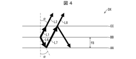
- the light-emitting element DX includes, in this order, a light-reflecting layer having a light-reflecting surface AA, a light-emitting layer having a light-emitting surface BB, and a light-semi-reflecting layer having a light-semi-reflecting surface CC.
- the light-semi-reflecting layer is located closer to the light-extracting side than the light-emitting layer.
- the distance from the light-reflecting surface AA to the light-semi-reflecting surface CC is the seventh distance f7
- the distance from the light-reflecting surface AA to the light-emitting surface BB is the eighth distance f8.
- the emission angle of the light ray with respect to the normal direction of the light-emitting surface BB is the angle ⁇ .
- the refractive index inside the light-emitting element DX is m, the absorption and refraction of light are ignored, and the light-reflecting surface AA, the light-emitting surface BB, and the light-semi-reflecting surface CC are assumed to be parallel planes to each other.
- light L1 emitted upward (to the light extraction side) from the light-emitting surface BB is split into light L2 that passes through the semi-reflective surface CC and light L3 that is reflected by the semi-reflective surface CC.
- the reflected light L3 becomes light L4 that is reflected by the semi-reflective surface AA, and is split into light L5 that passes through the semi-reflective surface CC and light that is reflected by the semi-reflective surface CC.
- the phases of light L2 and light L5 match, and light of wavelength ⁇ and its neighboring wavelengths are constructively coupled between the semi-reflective surface AA and the semi-reflective surface CC to form an optical resonator that selectively extracts light.
- the phases of light L2 and light L5 match.
- ⁇ is the circular constant
- N T is the order of resonance between the light reflecting surface AA and the light semi-reflecting surface CC
- ⁇ R is the phase shift due to reflection at the light reflecting surface AA
- ⁇ T is the phase shift due to reflection at the light semi-reflecting surface CC.
- the phase shifts ⁇ R and ⁇ T are set so that the minimum value of the order N T , which takes the resonator length as a positive value, is 1.
- ⁇ is the circular constant
- N R is the order of resonance between the light reflecting surface AA and the light emitting surface BB
- ⁇ R is the phase shift due to reflection at the light reflecting surface AA.
- the phase shift ⁇ R is set so that the minimum value of the order N R is 1.
- optical resonator in the light-emitting element DX can be applied to the optical resonators in the red, green, and blue light-emitting elements D1 to D3.
- the n-th order resonator lengths of the optical resonators in the red, green, and blue light-emitting elements D1 to D3 may be calculated or measured in a manner different from that described above.
- (Modification) 5 is a cross-sectional view showing a modified example of the configuration of a display device according to an embodiment of the present disclosure.
- lower charge functional layers J1, J2, and J3 of approximately the same thickness may be formed as a series of films JJ between the first light reflecting layer A1 and the first light emitting layer B1, between the second light reflecting layer A2 and the second light emitting layer B2, and between the third light reflecting layer A3 and the third light emitting layer B3.
- upper charge functional layers K1, K2, and K3 of approximately the same thickness may be formed as a series of films KK between the first light reflecting layer A1 and the common electrode CE, between the second light reflecting layer A2 and the common electrode CE, and between the third light reflecting layer A3 and the common electrode CE.
- the "series of films” refers to films formed in a single coating process in multiple pixels (multiple light emitting elements), for example, a film formed continuously across multiple pixels.
- the common electrode CE according to the second embodiment is made of silver (Ag) or an alloy containing silver, such as MgAg.
- the optical reflectance of a thin film of silver or a silver alloy is greater than that of a thin film of a transparent metal oxide. Therefore, according to the common electrode CE according to the second embodiment, the reinforcement effect of the optical resonator in the red, green, and blue light-emitting elements D1 to D3 is high, and the front brightness of the red, green, and blue light-emitting elements D1 to D3 can be improved.
- the thickness of the common electrode CE is small, and may be, for example, 15 to 30 nm.
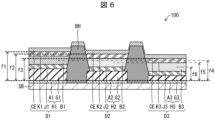
- FIG. 6 is a cross-sectional view showing an example of the configuration of a display device according to an embodiment of the present disclosure.
- FIG. 7 is a partial cross-sectional view showing an example of the configuration of the first light-emitting layer shown in FIG. 6.
- FIG. 8 is a partial cross-sectional view showing an example of the configuration of the second light-emitting layer shown in FIG. 6.
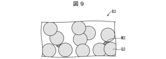
- FIG. 9 is a partial cross-sectional view showing an example of the configuration of the third light-emitting layer shown in FIG. 6. As shown in FIGS.
- the first light-emitting layer B1, the second light-emitting layer B2, and the third light-emitting layer B3 according to the third embodiment each include a plurality of quantum dots Q1, Q2, and Q3. At least one of the first light-emitting layer B1, the second light-emitting layer B2, and the third light-emitting layer B3 includes inorganic media M1 to M3 located between the plurality of quantum dots Q1, Q2, and Q3.
- the first light-emitting layer B1, the second light-emitting layer B2, and the third light-emitting layer B3 may be filled with inorganic media M1, M2, and M3 such that the filling rate of the first light-emitting layer B1>the filling rate of the second light-emitting layer B2>the filling rate of the third light-emitting layer B3.
- the third light-emitting layer B3 may not have the inorganic media M3.
- the refractive index of the cavity is usually smaller than the refractive index of the quantum dots Q1-Q3 and the inorganic media M1-M3.
- the filling rate of the light-emitting layer may be determined from the area ratio.
- a cross section of the first light-emitting layer B1 may be imaged using an electron microscope, and the total area of the quantum dots Q1 and the inorganic medium M1 in the image and the total cross-sectional area including the cavities of the first light-emitting layer B1 may be measured.
- the ratio of the total area of the quantum dots Q1 and the inorganic medium M1 to the total cross-sectional area may be determined as the filling rate of the first light-emitting layer B1.
- FIG. 10 is a cross-sectional view illustrating an example of a configuration of a display device according to an embodiment of the present disclosure.
- the display device 100 includes lower charge functional layers J1, J2, J3 formed with approximately the same thickness between the first light reflective layer A1 and the first light emitting layer B1, between the second light reflective layer A2 and the second light emitting layer B2, and between the third light reflective layer A3 and the third light emitting layer B3, upper charge functional layers K1, K2, K3 formed with approximately the same thickness between the first light reflective layer A1 and the common electrode CE, between the second light reflective layer A2 and the common electrode CE, and between the third light reflective layer A3 and the common electrode CE, and a bank layer BH located above the first light reflective layer A1, the second light reflective layer A2, and the third light reflective layer A3, and the first light emitting layer B1, the second light emitting layer B2, the third light emitting layer B3, the lower charge functional layers J1, J2, J3, and the upper charge functional layers K
- One of the lower charge functional layers J1, J2, J3 and the upper charge functional layers K1, K2, K3 may be a hole transport layer, and the other may be an electron transport layer.
- the first to third light emitting layers B1 to B3 are mounted on the bank layer BH together with the hole transport layer and the electron transport layer, respectively, and thus can emit light on the bank layer BH as well.
- an optical resonator can be formed for light from the first to third light emitting layers B1 to B3 on the bank layer BH, making it possible to effectively utilize the light emitted on the bank layer BH.
- the bank layer BH when the bank layer BH is substantially transparent and the optical distance from the upper surface of the bank layer BH on which the first light-emitting layer B1 lies to the first light-reflecting layer A1 is an integer multiple of the wavelength of red light, an optical resonator is formed in which the red light emitted on the upper surface of the bank layer BH reinforces each other.
- the bank layer BH is substantially transparent and the optical distance from the upper surface of the bank layer BH on which the second light-emitting layer B2 lies to the second light-reflecting layer A2 is an integer multiple of the wavelength of green light
- an optical resonator is formed in which the green light emitted on the upper surface of the bank layer BH reinforces each other.
- the bank layer BH is substantially transparent and the optical distance from the upper surface of the bank layer BH on which the third light-emitting layer B3 lies to the third light-reflecting layer A3 is an integer multiple of the wavelength of blue light, an optical resonator is formed in which the blue light emitted on the upper surface of the bank layer BH reinforces each other. In these cases, an error of about the half-width of the emission spectrum is allowed.
Landscapes
- Physics & Mathematics (AREA)
- Optics & Photonics (AREA)
- Engineering & Computer Science (AREA)
- Microelectronics & Electronic Packaging (AREA)
- Chemical & Material Sciences (AREA)
- Crystallography & Structural Chemistry (AREA)
- Inorganic Chemistry (AREA)
- Nanotechnology (AREA)
- Electroluminescent Light Sources (AREA)
Abstract
表示装置(100)は、第1光反射層(A1)、第1発光層(B1)および共通電極(CE)をこの順に含む赤色発光素子(D1)と、第2光反射層(A2)、第2発光層(B2)および共通電極(CE)をこの順に含む緑色発光素子(D2)と、第3光反射層(A3)、第3発光層(B3)および共通電極(CE)をこの順に含む青色発光素子(D3)とを備え、第1光反射層(A1)から共通電極(CE)までの距離を第1距離f1)、第2光反射層(A2)から共通電極(CE)までの距離を第2距離(f2)、第3光反射層(A3)から共通電極(CE)までの距離を第3距離(f3)、第1発光層(B1)の中心面から第1光反射層(A1)までの距離を第4距離(f4)、第2発光層(B2)の中心面から第2光反射層(A2)までの距離を第5距離(f5)、第3発光層(B3)の中心面から第3光反射層(A3)までの距離を第6距離(f6)として、第1距離(f1)>第2距離(f2)>第3距離(f3)、かつ第4距離(f4)>第5距離(f5)>第6距離(f6)である。
Description
本開示は、表示装置に関する。
特許文献1は、複数の画素が赤色(R)、緑色(G)、青色(B)に対応し、有機EL素子を構成する有機機能層の材質が対応する色にかかわらず共通であり、各画素に光共振器が構成され、発光層の厚さによって光共振器の光学長を赤色光、緑色光、青色光のいずれかに対応する長さに設定する有機EL装置を開示している。
特許文献1に開示の技術は、発光色ごとの共振長(共振器長)の設定を発光層の厚みの制御によって行うものであるため、何れかの色の発光素子の発光効率が低下する問題がある。
本開示の一態様に係る表示装置は、第1光反射層、第1発光層および共通電極をこの順に含む赤色発光素子と、第2光反射層、第2発光層および共通電極をこの順に含む緑色発光素子と、第3光反射層、第3発光層および共通電極をこの順に含む青色発光素子とを備え、前記第1光反射層から前記共通電極までの距離を第1距離、前記第2光反射層から前記共通電極までの距離を第2距離、前記第3光反射層から前記共通電極までの距離を第3距離、前記第1発光層の中心面から前記第1光反射層までの距離を第4距離、前記第2発光層の中心面から前記第2光反射層までの距離を第5距離、前記第3発光層の中心面から前記第3光反射層までの距離を第6距離として、前記第1距離>前記第2距離>前記第3距離、かつ前記第4距離>前記第5距離>前記第6距離である、構成である。
本開示の一態様によれば、発光素子の発光効率を向上させることができる。
〔実施形態1〕
図1は、本開示の一実施形態に係る表示装置の構成の一例を示す平面図である。図1に示すように、本開示に係る表示装置100は、複数の画素PXが設けられた表示部DAと、表示部DAを駆動する駆動回路DCとを備える。複数の画素PXは、赤色発光素子D1および画素回路E1を含む赤色画素P1と、緑色発光素子D2および画素回路E2を含む緑色画素P2と、青色発光素子D3および画素回路E3を含む青色画素P3と、を含む。以降、赤色発光素子D1、緑色発光素子D2および青色発光素子D3に注目する。
図1は、本開示の一実施形態に係る表示装置の構成の一例を示す平面図である。図1に示すように、本開示に係る表示装置100は、複数の画素PXが設けられた表示部DAと、表示部DAを駆動する駆動回路DCとを備える。複数の画素PXは、赤色発光素子D1および画素回路E1を含む赤色画素P1と、緑色発光素子D2および画素回路E2を含む緑色画素P2と、青色発光素子D3および画素回路E3を含む青色画素P3と、を含む。以降、赤色発光素子D1、緑色発光素子D2および青色発光素子D3に注目する。
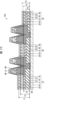
図2は、本開示の一実施形態に係る表示装置の構成の一例を示す断面図である。図2に示すように、表示装置100は、第1光反射層A1、第1発光層B1および共通電極CEをこの順に含む赤色発光素子D1と、第2光反射層A2、第2発光層B2および共通電極CEをこの順に含む緑色発光素子D2と、第3光反射層A3、第3発光層B3および共通電極CEをこの順に含む青色発光素子D3と、を備え、第1光反射層A1から共通電極CEまでの距離を第1距離f1、第2光反射層A2から共通電極CEまでの距離を第2距離f2、第3光反射層A3から共通電極CEまでの距離を第3距離f3、第1発光層B1の中心面から第1光反射層A1までの距離を第4距離f4、第2発光層B2の中心面から第2光反射層A2までの距離を第5距離f5、第3発光層B3の中心面から第3光反射層A3までの距離を第6距離f6として、第1距離f1>第2距離f2>第3距離f3、かつ、第4距離f4>第5距離f5>第6距離f6である。
本明細書において、単なる「距離」と記載した場合は、幾何学距離を意味する。光学距離を意図する場合は、「光学距離」と明示する。「厚さ」および「長さ」も同様に、「光学」と修飾しない限り、幾何学厚さおよび幾何学長さを意味する。距離、厚さおよび長さは、透過電子顕微鏡(TEM)による観察に基づいて決定してよく、あるいは、エリプソメトリーなど他の方法に基づいて決定してよい。
本明細書において、単なる「中心面」は、幾何学中心面、すなわち、上面および下面から幾何学的に等距離に位置する中間面を意味する。発光層に含まれる面(層厚方向に直交する面)のうち最も輝度が高い面を、「発光面」と記載する。
第1~第3光反射層A1~A3はそれぞれ、光反射電極または光反射電極の一部であっても、光透過電極よりも下層に形成された光反射膜であってもよい。第1~第3光反射層A1~A3は、同一材料から構成されてよく、同一層から形成されてよい。第1~第3光反射層A1~A3はそれぞれ、銀(Ag)、アルミニウム(Al)およびマグネシウム(Mg)とこれらの1つ以上を含む合金との何れかから構成されてよい。共通電極CEは、光透過性および光反射性を有し、第1~第3発光層B1~B3よりも光取り出し側に位置する。共通電極CEは、酸化インジウムスズ(InTiO)および酸化インジウム亜鉛(InZnO)などの透明金属酸化物からなってよい。
さらに、赤色発光素子D1は、第1光反射層A1および第1発光層B1の間に位置する第1光透過層G1を含み、緑色発光素子D2は、第2光反射層A2および第2発光層B2の間に位置する第2光透過層G2を含み、青色発光素子D3は、第3光反射層A3および第3発光層B3の間に位置する第3光透過層G3を含み、第1光透過層G1の厚さ>第2光透過層G2の厚さ>第3光透過層G3の厚さであってよい。
また、第1発光層B1の厚さ>第2発光層B2の厚さ>第3発光層B3の厚さであってよい。第1~第3発光層B1~B3はそれぞれ、発光材料として、有機発光材料を含んでも、量子ドットを含んでもよい。第1~第3発光層B1~B3は、屈折率が互いに略同一であってよい。赤色、緑色および青色発光素子D1~D3の電気特性が良好であるために、第1発光層B1および第3発光層B3の厚さの差が40〔nm〕以下であることが有益である。
第1光反射層A1と第1発光層B1との間、第2光反射層A2と第2発光層B2との間、および第3光反射層A3と第3発光層B3との間それぞれに、略同一厚さの下側電荷機能層J1,J2,J3が形成されていてよい。下側電荷機能層J1,J2,J3は、同一材料から構成されてよく、同一層から形成されてよい。また、第1発光層B1と共通電極CEとの間、第2発光層B2と共通電極CEとの間、および第3発光層B3と共通電極CEとの間それぞれに、略同一の厚さの上側電荷機能層K1,K2,K3が形成されていてよい。上側電荷機能層K1,K2,K3は、同一材料から構成されてよく、同一層から形成されてよい。赤色、緑色および青色発光素子D1~D3のそれぞれの平面視中央部で上側電荷機能層K1,K2,K3の厚さを測定し、上側電荷機能層K1,K2,K3の厚さにおける最大値と最小値との差異が10〔nm〕以下であるとき、上側電荷機能層K1,K2,K3の厚さを同一と見做してよい。
共通電極CEより上層は、共通電極CEよりも低屈折率(例えば、大気層)であってよい。
表示装置100は、第1~第3発光層B1~B3よりも上層の構成が、材料および層厚に関して赤色、緑色および青色発光素子D1~D3で共通である限り、第1~第3発光層B1~B3よりも上層に位置する追加の構成要素(不図示)を備えてもよい。表示装置100は、バンク層BH、赤色、緑色および青色発光素子D1~D3がその上に形成されている回路基板SB、ならびに、赤色、緑色および青色発光素子D1~D3を覆う封止層(不図示)などのその他の構成要素を適宜備えてよい。
赤色発光素子D1には、赤色光を強め合うための光共振器が形成され得る。そのため第1発光層B1は、赤色発光材料以外の発光材料を含んでよい。同様の理由で、第2発光層B2が緑色発光材料以外の発光材料を含んでよく、第3発光層B3が青色発光材料以外の発光材料を含んでよい。例えば、第1~第3発光層B1~B3が同一の発光材料群を含んでもよい。一方で、赤色発光素子D1の発光効率および輝度を向上するために、第1発光層B1中の発光材料においては、赤色発光材料の体積割合が最も高いことが有益である。同様の理由で、第2発光層B2中の発光材料においては、緑色発光材料の体積割合が最も高く、第3発光層B3中の発光材料においては、青色発光材料の体積割合が最も高いことが有益である。
発光材料の体積比は、面積比から判断してよい。例えば、第1発光層B1が発光材料として量子ドットを含む場合、第1発光層B1の断面を電子顕微鏡で撮像し、撮像画像における量子ドットの面積を計測し、該面積を発光色毎に合計し、赤色発光の量子ドットの合計面積が最大であるとき、第1発光層B1における最も体積比が高い量子ドットが赤色発光の量子ドットであると判断してよい。
共通電極CEがカソードであり、第1光反射層A1、第2光反射層A2および第3光反射層A3それぞれが、共通電極CEよりも下側に位置するアノードであってよい。加えて、または或いは、共通電極CEがカソードであり、第1光透過層G1、第2光透過層G2および第3光透過層G3それぞれが、共通電極CEよりも下側に位置するアノードであってよい。図2に示す例において、第1~第3光透過層G1~G3はそれぞれ、第1~第3光反射層A1~A3と接し、協働して第1~第3光反射電極H1~H3を構成し、第1~第3光反射電極H1~H3はそれぞれアノードである。これに限らず、第1~第3光透過層G1~G3はそれぞれ、第1~第3光反射層A1~A3から分離していてよい。
共通電極CEがアノードであり、第1~第3光反射層A1~A3それぞれが、共通電極CEよりも下側に位置するカソードであってよい。加えて、または或いは、共通電極CEがアノードであり、第1~第3光透過層G1~G3それぞれが、共通電極CEよりも下側に位置するカソードであってよい。
第1~第3光透過層G1~G3は、屈折率が互いに略同一であってよい。第1~第3光透過層G1~G3は、同一材料から構成されてよい。第1光透過層G1、第2光透過層G2、および第3光透過層G1~G3それぞれが、酸化インジウムスズ(InTiO)および酸化インジウム亜鉛(InZnO)などの透明金属酸化物からなってよい。
(光共振器)
赤色発光素子D1中に、赤色光が強め合う1つ以上の光共振器が形成され得る。赤色光の波長は、600~770〔nm〕である。第1距離f1は、赤色光が、第1光反射層A1および共通電極CE間で強め合うためのn次共振器長であってよく、このとき、第1光反射層A1および共通電極CE間に、赤色光が強め合う光共振器が形成される。また、第1発光層B1の発光面から第1光反射層A1までの距離は、赤色光が、第1発光層B1の発光面および第1光反射層A1間で強め合うためのn次共振器長であってよく、このとき、第1発光層B1の発光面および第1光反射層A1間に、赤色光が強め合う光共振器が形成される。「n次共振器長」の「n」は任意の自然数である。
赤色発光素子D1中に、赤色光が強め合う1つ以上の光共振器が形成され得る。赤色光の波長は、600~770〔nm〕である。第1距離f1は、赤色光が、第1光反射層A1および共通電極CE間で強め合うためのn次共振器長であってよく、このとき、第1光反射層A1および共通電極CE間に、赤色光が強め合う光共振器が形成される。また、第1発光層B1の発光面から第1光反射層A1までの距離は、赤色光が、第1発光層B1の発光面および第1光反射層A1間で強め合うためのn次共振器長であってよく、このとき、第1発光層B1の発光面および第1光反射層A1間に、赤色光が強め合う光共振器が形成される。「n次共振器長」の「n」は任意の自然数である。
人間の視感度が555〔nm〕近傍で、すなわち赤色光より短波長側で、最も高い。これを考慮して、上記距離をそれぞれn次共振器長より短く設計してもよい。また、簡単化のために、第1発光層B1の発光面を、第1発光層B1の幾何学中心面に置き換えてよい。具体的には、第1距離f1は、赤色光が、第1光反射層A1および共通電極CE間で強め合うための共振器長に対して、n次共振器長をR1,nとして、第1距離f1がn次共振器長R1,n以下であり、かつ、第1距離f1とn次共振器長R1,nとの差分が、(n-1)次共振器長R1,n-1とn次共振器長R1,nとの差分の2割以下であってよい。差分は絶対値である。すなわち、下記不等式(1)を満たしてよい。ただし、位相ずれと無関係に、0次共振器長R1,0を0〔nm〕とする。

また、第4距離f4は、赤色光が、第1発光層B1の中心面および第1光反射層A1間で強め合うための共振器長に対して、n次共振器長をR4,nとして、第4距離f4がn次共振器長R4,n以下であり、かつ、第4距離f4とn次共振器長R4,nとの差分が、(n-1)次共振器長R4,n-1とn次共振器長R4,nとの差分の2割以下であってよい。差分は絶対値である。すなわち、下記不等式(2)を満たしてよい。ただし、位相ずれと無関係に、0次共振器長R4,0を0〔nm〕とする。

緑色発光素子D2中に、緑色光が強め合う1つ以上の光共振器が形成され得る。緑色光の波長は、490~550〔nm〕である。第2距離f2は、緑色光が、第2光反射層A2および共通電極CE間で強め合うためのn次共振器長であってよく、このとき、第2光反射層A2および共通電極CE間に、緑色光が強め合う光共振器が形成される。また、第2発光層B2の発光面から第2光反射層A2までの距離は、緑色光が、第2発光層B2の発光面および第2光反射層A2間で強め合うためのn次共振器長であってよく、このとき、第2発光層B2の発光面および第2光反射層A2間に、緑色光が強め合う光共振器が形成される。
人間の視感度が緑色光より長波長側で最も高いことを考慮して、上記距離をそれぞれn次共振器長より長く設計してもよい。また、簡単化のために、第2発光層B2の発光面を、第2発光層B2の幾何学中心面に置き換えてよい。具体的には、第2距離f2は、緑色光が、第2光反射層A2および共通電極CE間で強め合うための共振器長に対して、n次共振器長をR2,nとして、第2距離f2がn次共振器長R2,n以上であり、かつ、第2距離f2とn次共振器長R2,nとの差分が、(n+1)次共振器長R2,n+1とn次共振器長R2,nとの差分の2割以下であってよい。差分は絶対値である。すなわち、下記不等式(3)を満たしてよい。ただし、位相ずれと無関係に、0次共振器長R2,0を0〔nm〕とする。

また、第5距離f5は、緑色光が、第2発光層B2の中心面および第2光反射層A2間で強め合うための共振器長に対して、n次共振器長をR5,nとして、第5距離f5がn次共振器長R5,n以上であり、かつ、第5距離f5とn次共振器長R5,nとの差分が、(n+1)次共振器長R5,n+1とn次共振器長R5,nとの差分の2割以下であってよい。差分は絶対値である。すなわち、下記不等式(4)を満たしてよい。ただし、位相ずれと無関係に、0次共振器長R5,0を0〔nm〕とする。

青色発光素子D3中に、青色光が強め合う1つ以上の光共振器が形成され得る。青色光の波長は、430~490〔nm〕である。第3距離f3は、青色光が、第3光反射層A3および共通電極CE間で強め合うためのn次共振器長であってよく、このとき、第3光反射層A3および共通電極CE間に、青色光が強め合う光共振器が形成される。また、第3発光層B3の発光面から第3光反射層A3までの距離は、青色光が、第3発光層B3の発光面および第3光反射層A3間で強め合うためのn次共振器長であってよく、このとき、第3発光層B3の発光面および第3光反射層A3間に、青色光が強め合う光共振器が形成される。
人間の視感度が青色光より長波長側で最も高いことを考慮して、上記距離をそれぞれn次共振器長より長く設計してもよい。また、簡単化のために、第3発光層B3の発光面を、第3発光層B3の幾何学中心面に置き換えてよい。具体的には、第3距離f3は、青色光が、第3光反射層A3および共通電極CE間で強め合うための共振器長に対して、n次共振器長をR3,nとして、第3距離f3がn次共振器長R3,n以上であり、かつ、第3距離f3とn次共振器長R3,nとの差分が、(n+1)次共振器長R3,n+1とn次共振器長R3,nとの差分の2割以下であってよい。差分は絶対値である。すなわち、下記不等式(5)を満たしてよい。ただし、位相ずれと無関係に、0次共振器長R3,0を0〔nm〕とする。

また、第6距離f6は、青色光が、第3発光層B3の中心面および第3光反射層A3間で強め合うための共振器長に対して、n次共振器長をR6,nとして、第6距離f6がn次共振器長R6,n以上であり、かつ、第6距離f6とn次共振器長R6,nとの差分が、(n+1)次共振器長R6,n+1とn次共振器長R6,nとの差分の2割以下であってよい。差分は絶対値である。すなわち、下記不等式(6)を満たしてよい。ただし、位相ずれと無関係に、0次共振器長R5,0を0〔nm〕とする。

第1発光層B1の発光面および第1光反射層A1間に形成される光共振器に関し、当該光共振器の長さが一次共振器長であるとき、プラズモン損失が発生しやすい。また、当該光共振器の長さが三次以上の共振器長であるとき、当該光共振器による色ずれが大きい。したがって、当該共振器の長さは二次共振器長またはその近傍値であることが有益である。同様の理由で、第2発光層B2の発光面および第2光反射層A2間に形成される光共振器と、第3発光層B3の発光面および第3光反射層A3間に形成される光共振器との長さも、二次共振器長またはその前後の長さであることが有益である。したがって、第4距離f4は、赤色光が、第1発光層B1の中心面および第1光反射層A1間で強め合うための共振器長に対して、n次共振器長をR4,nとして、第4距離f4が、2次共振器長R4,2から1次共振器長R4,1と2次共振器長R4,2との差分の2割を引いた値以上、かつ、2次共振器長R4,2に3次共振器長R4,3と2次共振器長R4,2との差分の2割を加えた値以下であってよい。同様に、第5距離f5は、緑色光が、第2発光層B2の中心面および第2光反射層A2間で強め合うための共振器長に対して、n次共振器長をR5,nとして、第5距離f5が、2次共振器長R5,2から1次共振器長R5,1と2次共振器長R5,2との差分の2割を引いた値以上、2次共振器長R5,2に3次共振器長R5,3と2次共振器長R5,2との差分の2割を加えた値以下であってよい。また、第6距離f6は、青色光が、第3発光層B3の中心面および第3光反射層A3間で強め合うための共振器長に対して、n次共振器長をR6,nとして、第6距離f6が、2次共振器長R6,2から1次共振器長R6,1と2次共振器長R6,2との差分を引いた値以上、2次共振器長R6,2に3次共振器長R6,3と2次共振器長R6,2との差分の2割を加えた値以下であってよい。何れについても差分は絶対値である。
すなわち、下記連立不等式(7)を満たしてよい。

第1発光層B1および第3発光層B3の厚さの差が40〔nm〕以下であるために、第1~第3発光層B1~B3の発光面から共通電極CEまでの距離がそれぞれ、一次共振器長またはその前後の長さであることが有益である。したがって、第1距離f1と第4距離f4との差分は、赤色光が、第1発光層B1の中心面および共通電極CE間で強め合うための共振器長に対して、n次共振器長をR7,nとして、第1距離f1と第4距離f4との差分が、1次共振器長R7,1から0次共振器長R7,0と1次共振器長R7,1との差分の2割を引いた値以上、かつ、1次共振器長R7,1に2次共振器長R7,2と1次共振器長R7,1との差分の2割を加えた値以下であってよい。同様に、第2距離f2と第5距離f5との差分は、緑色光が、第2発光層B2の中心面および共通電極CE間で強め合うための共振器長に対して、n次共振器長をR8,nとして、第2距離f2と第5距離f5との差分が、1次共振器長R8,1から0次共振器長R8,0と1次共振器長R8,1との差分の2割を引いた値以上、かつ、1次共振器長R8,1に2次共振器長R8,2と1次共振器長R8,1との差分の2割を加えた値以下であってよい。また、第3距離f3と第6距離f6との差分は、第3発光層B3の中心面および共通電極CE間で強め合うための共振器長に対して、n次共振器長をR9,nとして、第3距離f3と第6距離f6との差分が、1次共振器長R9,1から0次共振器長R9,0と1次共振器長R9,1との差分の2割を引いた値以上、かつ、1次共振器長R9,1に2次共振器長R9,2と1次共振器長R9,1との差分の2割を加えた値以下であってよい。何れについても0次共振器長R7,0,R8,0,R9,nは0〔nm〕であり、差分は絶対値である。
すなわち、下記連立不等式(8)を満たしてよい。

人間の視感度、反射の位相ずれ、および発光層内での発光位置を考慮すると、第3距離f3の青色発光素子D3の発光ピーク波長に対する比>第2距離f2の緑色発光素子D2の発光ピーク波長に対する比>第1距離f1の赤色発光素子D1の発光ピーク波長に対する比であってよい。また、第6距離f6の青色発光素子D3の発光ピーク波長に対する比>第5距離f5の緑色発光素子D2の発光ピーク波長に対する比>第4距離f4の赤色発光素子D1の発光ピーク波長に対する比であってよい。
(n次共振器長)
図3および図4はそれぞれ、発光素子に形成され得る光共振器を説明する図である。図3および図4に示すように、発光素子DXは、光反射面AAを有する光反射層と、発光面BBを有する発光層と、光半反射面CCを有する光半反射層と、をこの順に含む。光半反射層は、発光層よりも光取り出し側に位置する。光反射面AAから光半反射面CCまでの距離を第7距離f7とし、光反射面AAから発光面BBまでの距離を第8距離f8とする。また、発光面BBの法線方向に対する光線の出射角を角度αとする。以降、説明の簡単化のために、発光素子DX内部における屈折率をmとし、光の吸収および屈折を無視し、光反射面AAと発光面BBと光半反射面CCとを互いに平行な平面であるとする。
図3および図4はそれぞれ、発光素子に形成され得る光共振器を説明する図である。図3および図4に示すように、発光素子DXは、光反射面AAを有する光反射層と、発光面BBを有する発光層と、光半反射面CCを有する光半反射層と、をこの順に含む。光半反射層は、発光層よりも光取り出し側に位置する。光反射面AAから光半反射面CCまでの距離を第7距離f7とし、光反射面AAから発光面BBまでの距離を第8距離f8とする。また、発光面BBの法線方向に対する光線の出射角を角度αとする。以降、説明の簡単化のために、発光素子DX内部における屈折率をmとし、光の吸収および屈折を無視し、光反射面AAと発光面BBと光半反射面CCとを互いに平行な平面であるとする。
図3に示すように、発光面BBから上方(光取り出し側)に出射された光L1は、光半反射面CCを通過した光L2と、光半反射面CCで反射された光L3とに分かれる。反射された光L3は、光反射面AAで反射された光L4となり、光半反射面CCを通過した光L5と、光半反射面CCで反射された光とに分かれる。所望の波長λにおいて、下記の強め合いの条件式(9)を満たすとき、光L2と光L5との位相(あるいは、光L1と光L4との位相)が整合し、光反射面AAと光半反射面CCとの間に波長λおよびその近傍波長の光が強め合って、選択的に取り出される光共振器が形成される。特に、発光素子DXの正面への光の取り出しに関し、cosα=1であり、下記の強め合いの条件式(10)を満たすときに、光L2と光L5との位相が整合する。


図4に示すように、光L1と同位相かつ同一出射角度で、発光面BBから下方(光取り出し側の反対側)に出射された光L6は、光反射面AAで反射された光L7となり、光半反射面CCを通過した光L8と、光半反射面CCで反射された光とに分かれる。所望の波長λにおいて、下記の強め合いの条件式(11)を満たすとき、光L2と光L8との位相(あるいは、光L1と光L7との位相)が整合し、光反射面AAと発光面BBとの間に波長λおよびその近傍波長の光が強め合って、選択的に取り出される光共振器が形成される。特に、発光素子DXの正面への光の取り出しに関し、cosα=1であり、下記の強め合いの条件式(12)を満たすときに、光L2と光L8との位相が整合する。


したがって、波長λの光が光反射面AAと光半反射面CCとの間で強め合うためのn次共振器長は、n=NTとして、下記式(13)で表される。また、波長λの光が発光面BBと光反射面AAとの間で強め合うためのn次共振器長は、n=NRとして、下記式(14)で表される。


(変形例)
図5は、本開示の一実施形態に係る表示装置の構成の変形例を示す断面図である。図5に示すように、第1光反射層A1と第1発光層B1との間、第2光反射層A2と第2発光層B2との間、および第3光反射層A3と第3発光層B3との間にわたって、略同一厚さの下側電荷機能層J1,J2,J3が一連の膜JJとして形成されていてよい。また、第1光反射層A1と共通電極CEとの間、第2光反射層A2と共通電極CEとの間、および第3光反射層A3と共通電極CEとの間にわたって、略同一の厚さの上側電荷機能層K1,K2,K3が一連の膜KKとして形成されていてよい。ここで「一連の膜」とは、複数の画素(複数の発光素子)において単一の塗布工程で作成される膜であり、例えば、複数の画素に渡って連続して形成される膜である。
図5は、本開示の一実施形態に係る表示装置の構成の変形例を示す断面図である。図5に示すように、第1光反射層A1と第1発光層B1との間、第2光反射層A2と第2発光層B2との間、および第3光反射層A3と第3発光層B3との間にわたって、略同一厚さの下側電荷機能層J1,J2,J3が一連の膜JJとして形成されていてよい。また、第1光反射層A1と共通電極CEとの間、第2光反射層A2と共通電極CEとの間、および第3光反射層A3と共通電極CEとの間にわたって、略同一の厚さの上側電荷機能層K1,K2,K3が一連の膜KKとして形成されていてよい。ここで「一連の膜」とは、複数の画素(複数の発光素子)において単一の塗布工程で作成される膜であり、例えば、複数の画素に渡って連続して形成される膜である。
〔実施形態2〕
本開示の他の実施形態について、以下に説明する。なお、説明の便宜上、上記実施形態にて説明した部材と同じ機能を有する部材については、同じ符号を付記し、その説明を繰り返さない。
本開示の他の実施形態について、以下に説明する。なお、説明の便宜上、上記実施形態にて説明した部材と同じ機能を有する部材については、同じ符号を付記し、その説明を繰り返さない。
本実施形態2に係る共通電極CEは、銀(Ag)またはMgAgなどの銀を含む合金からなる。銀または銀合金の薄膜の光反射率は、透明金属酸化物の薄膜の光反射率よりも大きい。したがって、本実施形態2に係る共通電極CEによれば、赤色、緑色および青色発光素子D1~D3における光共振器による強め合い効果が高く、赤色、緑色および青色発光素子D1~D3の正面輝度を向上できる。一方で、銀または銀合金による光吸収を低減するために、共通電極CEの厚みは、小さいことが好ましく、例えば、15~30〔nm〕であってよい。
〔実施形態3〕
図6は、本開示の一実施形態に係る表示装置の構成の一例を示す断面図である。図7は、図6に示した第1発光層の構成の一例を示す部分断面図である。図8は、図6に示した第2発光層の構成の一例を示す部分断面図である。図9は、図6に示した第3発光層の構成の一例を示す部分断面図である。図6~図9に示すように、本実施形態3に係る第1発光層B1、第2発光層B2および第3発光層B3それぞれが、複数の量子ドットQ1,Q2,Q3を含む。第1発光層B1、第2発光層B2および第3発光層B3の少なくとも1つが、複数の量子ドットQ1,Q2,Q3の間に位置する無機媒体M1~M3を含む。
図6は、本開示の一実施形態に係る表示装置の構成の一例を示す断面図である。図7は、図6に示した第1発光層の構成の一例を示す部分断面図である。図8は、図6に示した第2発光層の構成の一例を示す部分断面図である。図9は、図6に示した第3発光層の構成の一例を示す部分断面図である。図6~図9に示すように、本実施形態3に係る第1発光層B1、第2発光層B2および第3発光層B3それぞれが、複数の量子ドットQ1,Q2,Q3を含む。第1発光層B1、第2発光層B2および第3発光層B3の少なくとも1つが、複数の量子ドットQ1,Q2,Q3の間に位置する無機媒体M1~M3を含む。
第1発光層B1、第2発光層B2および第3発光層B3には、第1発光層B1の充填率>第2発光層B2の充填率>第3発光層B3の充填率となるように、無機媒体M1,M2,M3が充填されてよい。なお、第3発光層B3に無機媒体M3が無くてもよい。空洞の屈折率は通常、量子ドットQ1~Q3および無機媒体M1~M3の屈折率より小さい。これによって、第1~第3発光層B1~B3の厚さが略同一であり、量子ドットQ1~Q3および無機媒体M1~M3の屈折率が略同一であるときに、第1発光層B1の光学厚さ>第2発光層B2の光学厚さ>第3発光層B3の光学厚さとなる。したがって、第1~第3発光層B1~B3の厚みの差を低減しつつ、表示装置100の光学構造および電気構造を最適化することができる。例えば、第1発光層B1および第3発光層B3の厚さの差が40〔nm〕以下であるようにし易い。
発光層の充填率は、面積比から判断してよい。例えば、第1発光層B1の断面を電子顕微鏡で撮像し、撮像画像における量子ドットQ1および無機媒体M1の合計面積と、第1発光層B1の空洞を含む全断面積と、を計測し、全断面積に対する量子ドットQ1および無機媒体M1の合計面積の比を、第1発光層B1の充填率としてよい。
〔実施形態4〕
図10は、本開示の一実施形態に係る表示装置の構成の一例を示す断面図である。図10に示すように、表示装置100が、第1光反射層A1と第1発光層B1との間、第2光反射層A2と第2発光層B2との間、および第3光反射層A3と第3発光層B3との間にわたって略同一厚さで形成された下側電荷機能層J1,J2,J3と、第1光反射層A1と共通電極CEとの間、第2光反射層A2と共通電極CEとの間、および第3光反射層A3と共通電極CEとの間にわたって略同一の厚さで形成された上側電荷機能層K1,K2,K3と、第1光反射層A1、第2光反射層A2および第3光反射層A3よりも上層に位置するバンク層BHとを備え、第1発光層B1、第2発光層B2、第3発光層B3、下側電荷機能層J1,J2,J3、および上側電荷機能層K1,K2,K3がバンク層BHに乗り上げてよい。
図10は、本開示の一実施形態に係る表示装置の構成の一例を示す断面図である。図10に示すように、表示装置100が、第1光反射層A1と第1発光層B1との間、第2光反射層A2と第2発光層B2との間、および第3光反射層A3と第3発光層B3との間にわたって略同一厚さで形成された下側電荷機能層J1,J2,J3と、第1光反射層A1と共通電極CEとの間、第2光反射層A2と共通電極CEとの間、および第3光反射層A3と共通電極CEとの間にわたって略同一の厚さで形成された上側電荷機能層K1,K2,K3と、第1光反射層A1、第2光反射層A2および第3光反射層A3よりも上層に位置するバンク層BHとを備え、第1発光層B1、第2発光層B2、第3発光層B3、下側電荷機能層J1,J2,J3、および上側電荷機能層K1,K2,K3がバンク層BHに乗り上げてよい。
下側電荷機能層J1,J2,J3および上側電荷機能層K1,K2,K3の一方が正孔輸送層であり、他方が電子輸送層であってよい。第1~第3発光層B1~B3はそれぞれ、正孔輸送層および電子輸送層と共にバンク層BHに乗り上げていることによって、バンク層BH上でも発光し得る。また、バンク層BH上の第1~第3発光層B1~B3からの光に対しても光共振器を形成して、バンク層BH上での発光を有効利用できる。
例えば、バンク層BHが実質的に透明であり、第1発光層B1が乗り上げているバンク層BHの上面から第1光反射層A1までの光学距離が、赤色光の波長の整数倍であるとき、バンク層BHの上面で発光された赤色光を強め合う光共振器が形成される。バンク層BHが実質的に透明であり、第2発光層B2が乗り上げているバンク層BHの上面から第2光反射層A2までの光学距離が、緑色光の波長の整数倍であるとき、バンク層BHの上面で発光された緑色光を強め合う光共振器が形成される。バンク層BHが実質的に透明であり、第3発光層B3が乗り上げているバンク層BHの上面から第3光反射層A3までの光学距離が、青色光の波長の整数倍であるとき、バンク層BHの上面で発光された青色光を強め合う光共振器が形成される。これらにおいて、発光スペクトルの半値幅程度の誤差が許容される。
本開示は上述した各実施形態に限定されるものではなく、請求項に示した範囲で種々の変更が可能であり、異なる実施形態にそれぞれ開示された技術的手段を適宜組み合わせて得られる実施形態についても本開示の技術的範囲に含まれる。さらに、各実施形態にそれぞれ開示された技術的手段を組み合わせることにより、新しい技術的特徴を形成することができる。
100 表示装置
A1 第1光反射層
A2 第2光反射層
A3 第3光反射層
B1 第1発光層
B2 第2発光層
B3 第3発光層
CE 共通電極
D1 赤色発光素子
D2 緑色発光素子
D3 青色発光素子
f1 第1距離
f2 第2距離
f3 第3距離
f4 第4距離
f5 第5距離
f6 第6距離
G1 第1光透過層
G2 第2光透過層
G3 第3光透過層
J1~J3 下側電荷機能層
JJ 一連の膜
K1~K3 上側電荷機能層
KK 一連の膜
M1~M3 無機媒体
Q1~Q3 量子ドット
A1 第1光反射層
A2 第2光反射層
A3 第3光反射層
B1 第1発光層
B2 第2発光層
B3 第3発光層
CE 共通電極
D1 赤色発光素子
D2 緑色発光素子
D3 青色発光素子
f1 第1距離
f2 第2距離
f3 第3距離
f4 第4距離
f5 第5距離
f6 第6距離
G1 第1光透過層
G2 第2光透過層
G3 第3光透過層
J1~J3 下側電荷機能層
JJ 一連の膜
K1~K3 上側電荷機能層
KK 一連の膜
M1~M3 無機媒体
Q1~Q3 量子ドット
Claims (31)
- 第1光反射層、第1発光層および共通電極をこの順に含む赤色発光素子と、第2光反射層、第2発光層および共通電極をこの順に含む緑色発光素子と、第3光反射層、第3発光層および共通電極をこの順に含む青色発光素子とを備え、
前記第1光反射層から前記共通電極までの距離を第1距離、
前記第2光反射層から前記共通電極までの距離を第2距離、
前記第3光反射層から前記共通電極までの距離を第3距離、
前記第1発光層の中心面から前記第1光反射層までの距離を第4距離、
前記第2発光層の中心面から前記第2光反射層までの距離を第5距離、
前記第3発光層の中心面から前記第3光反射層までの距離を第6距離として、
前記第1距離>前記第2距離>前記第3距離、かつ前記第4距離>前記第5距離>前記第6距離である、表示装置。 - 前記赤色発光素子は、前記第1光反射層および前記第1発光層間に位置する第1光透過層を含み、
前記緑色発光素子は、前記第2光反射層および前記第2発光層間に位置する第2光透過層を含み、
前記青色発光素子は、前記第3光反射層および前記第3発光層間に位置する第3光透過層を含み、
前記第1光透過層の厚さ>前記第2光透過層の厚さ>前記第3光透過層の厚さである、請求項1に記載の表示装置。 - 前記共通電極がカソードであり、
前記第1光透過層、前記第2光透過層および前記第3光透過層それぞれが、前記共通電極よりも下側に位置するアノードである、請求項2に記載の表示装置。 - 前記第1光透過層、前記第2光透過層、および前記第3光透過層それぞれが透明金属酸化物からなる、請求項2または3に記載の表示装置。
- 前記第1発光層の厚さ>前記第2発光層の厚さ>前記第3発光層の厚さである、請求項1~4の何れか1項に記載の表示装置。
- 前記第1光反射層と前記第1発光層との間、前記第2光反射層と前記第2発光層との間、および前記第3光反射層と前記第3発光層との間それぞれに、同一厚さの下側電荷機能層が形成されている、請求項1~5のいずれか1項に記載の表示装置。
- 前記第1光反射層と前記第1発光層との間、前記第2光反射層と前記第2発光層との間、および前記第3光反射層と前記第3発光層との間にわたって、同一厚さの下側電荷機能層が一連の膜として形成されている、請求項1~5のいずれか1項に記載の表示装置。
- 前記第1発光層と前記共通電極との間、前記第2発光層と前記共通電極との間、および前記第3発光層と前記共通電極との間それぞれに、同一厚さの上側電荷機能層が形成されている、請求項1~7のいずれか1項に記載の表示装置。
- 前記第1発光層と前記共通電極との間、前記第2発光層と前記共通電極との間、および前記第3発光層と前記共通電極との間にわたって、同一厚さの上側電荷機能層が一連の膜として形成されている、請求項1~7のいずれか1項に記載の表示装置。
- 前記第1発光層中の発光材料においては、赤色発光材料の体積割合が最も高く、
前記第2発光層中の発光材料においては、緑色発光材料の体積割合が最も高く、
前記第3発光層中の発光材料においては、青色発光材料の体積割合が最も高い、請求項1~9のいずれか1項に記載の表示装置。 - 前記第1発光層、前記第2発光層および前記第3発光層それぞれが複数の量子ドットを含む、請求項1~10のいずれか1項に記載の表示装置。
- 前記第1発光層、前記第2発光層および前記第3発光層の少なくとも1つが、前記複数の量子ドットの間に位置する無機媒体を含む、請求項11に記載の表示装置。
- 前記第1発光層、前記第2発光層および前記第3発光層には、前記第1発光層の充填率>前記第2発光層の充填率>前記第3発光層の充填率となるように無機媒体が充填されている、請求項12に記載の表示装置。
- 前記第1発光層および前記第3発光層の厚さの差が40〔nm〕以下である、請求項1~13のいずれか1項に記載の表示装置。
- 赤色光が前記第1光反射層および前記共通電極間で強め合うための共振器長に対して、前記第1距離がn次共振器長以下であり、かつ、前記第1距離とn次共振器長との差分が、(n-1)次共振器長とn次共振器長との差分の2割以下である、請求項1~14のいずれか1項に記載の表示装置。
- 緑色光が前記第2光反射層および前記共通電極間で強め合うための共振器長に対して、前記第2距離がn次共振器長以上であり、かつ、前記第2距離とn次共振器長との差分が、(n+1)次共振器長とn次共振器長との差分の2割以下である、請求項1~15のいずれか1項に記載の表示装置。
- 青色光が前記第3光反射層および前記共通電極間で強め合うための共振器長に対して、前記第3距離がn次共振器長以上であり、かつ、前記第3距離とn次共振器長との差分が、(n+1)次共振器長とn次共振器長との差分の2割以下である、請求項1~16のいずれか1項に記載の表示装置。
- 赤色光が前記第1発光層の中心面および前記第1光反射層間で強め合うための共振器長に対して、前記第4距離がn次共振器長以下であり、かつ、前記第4距離とn次共振器長との差分が、(n-1)次共振器長とn次共振器長との差分の2割以下である、請求項1~17のいずれか1項に記載の表示装置。
- 緑色光が前記第2発光層の中心面および前記第2光反射層間で強め合うための共振器長に対して、前記第5距離がn次共振器長以上であり、かつ、前記第5距離とn次共振器長との差分が、(n+1)次共振器長とn次共振器長との差分の2割以下である、請求項1~18のいずれか1項に記載の表示装置。
- 青色光が前記第3発光層の中心面および前記第3光反射層間で強め合うための共振器長に対して、前記第6距離がn次共振器長以上であり、かつ、前記第6距離とn次共振器長との差分が、(n+1)次共振器長とn次共振器長との差分の2割以下である、請求項1~19のいずれか1項に記載の表示装置。
- 前記共通電極がカソードであり、
前記第1光反射層、前記第2光反射層および前記第3光反射層それぞれが、前記共通電極よりも下側に位置するアノードである、請求項1~20の何れか1項に記載の表示装置。 - 前記第4距離は、赤色光が前記第1発光層の中心面および前記第1光反射層間で強め合うための共振器長に対して、2次共振器長から1次共振器長と2次共振器長との差分の2割を引いた値以上、かつ、2次共振器長に3次共振器長と2次共振器長との差分の2割を加えた値以下であり、
前記第5距離は、緑色光が前記第2発光層の中心面および前記第2光反射層間で強め合うための共振器長に対して、2次共振器長から1次共振器長と2次共振器長との差分の2割を引いた値以上、かつ、2次共振器長に3次共振器長と2次共振器長との差分の2割を加えた値以下であり、
前記第6距離は、青色光が前記第3発光層の中心面および前記第3光反射層間で強め合うための共振器長に対して、2次共振器長から1次共振器長と2次共振器長との差分の2割を引いた値以上、かつ、2次共振器長に3次共振器長と2次共振器長との差分の2割を加えた値以下である、請求項1~21のいずれか1項に記載の表示装置。 - 前記第1距離と前記第4距離との差分は、赤色光が前記第1発光層の中心面および前記共通電極間で強め合うための共振器長に対して、1次共振器長から0次共振器長と1次共振器長との差分の2割を引いた値以上、かつ、1次共振器長に2次共振器長と1次共振器長との差分の2割を加えた値以下であり、
前記第2距離と前記第5距離との差分は、緑色光が前記第2発光層の中心面および前記共通電極間で強め合うための共振器長に対して、1次共振器長から0次共振器長と1次共振器長との差分の2割を引いた値以上、かつ、1次共振器長に2次共振器長と1次共振器長との差分の2割を加えた値以下であり、
前記第3距離と前記第6距離との差分は、青色光が前記第3発光層の中心面および前記共通電極間で強め合うための共振器長に対して、1次共振器長から0次共振器長と1次共振器長との差分の2割を引いた値以上、かつ、1次共振器長に2次共振器長と1次共振器長との差分の2割を加えた値以下である、請求項1~22のいずれか1項に記載の表示装置。 - 前記第1光反射層と前記第1発光層との間、前記第2光反射層と前記第2発光層との間、および前記第3光反射層と前記第3発光層との間にわたって同一の厚さで形成された下側電荷機能層と、
前記第1発光層と前記共通電極との間、前記第2発光層と前記共通電極との間、および前記第3発光層と前記共通電極との間にわたって同一の厚さで形成された上側電荷機能層と、
前記第1光反射層、前記第2光反射層および前記第3光反射層よりも上層に位置するバンク層とを備え、
前記第1発光層、前記第2発光層、前記第3発光層、前記下側電荷機能層、および前記上側電荷機能層が前記バンク層に乗り上げている、請求項1~23のいずれか1項に記載の表示装置。 - 前記下側電荷機能層および前記上側電荷機能層の一方が正孔輸送層であって他方が電子輸送層である、請求項24に記載の表示装置。
- 前記共通電極は、光透過性および光反射性を有し、前記第1発光層、前記第2発光層、および前記第3発光層よりも光取り出し側に位置する、請求項1~25のいずれか1項に記載の表示装置。
- 前記共通電極は、銀または銀を含む合金からなる、請求項1~26のいずれか1項に記載の表示装置。
- 前記共通電極の厚みは、15~30〔nm〕である、請求項27に記載の表示装置。
- 前記共通電極は、透明金属酸化物からなる、請求項1~28のいずれか1項に記載の表示装置。
- 前記第3距離の前記青色発光素子の発光ピーク波長に対する比>前記第2距離の前記緑色発光素子の発光ピーク波長に対する比>前記第1距離の前記赤色発光素子の発光ピーク波長に対する比である、請求項1~29のいずれか1項に記載の表示装置。
- 前記第6距離の前記青色発光素子の発光ピーク波長に対する比>前記第5距離の前記緑色発光素子の発光ピーク波長に対する比>前記第4距離の前記赤色発光素子の発光ピーク波長に対する比である、請求項1~30のいずれか1項に記載の表示装置。
Priority Applications (1)
| Application Number | Priority Date | Filing Date | Title |
|---|---|---|---|
| PCT/JP2023/012590 WO2024201729A1 (ja) | 2023-03-28 | 2023-03-28 | 表示装置 |
Applications Claiming Priority (1)
| Application Number | Priority Date | Filing Date | Title |
|---|---|---|---|
| PCT/JP2023/012590 WO2024201729A1 (ja) | 2023-03-28 | 2023-03-28 | 表示装置 |
Publications (1)
| Publication Number | Publication Date |
|---|---|
| WO2024201729A1 true WO2024201729A1 (ja) | 2024-10-03 |
Family
ID=92903561
Family Applications (1)
| Application Number | Title | Priority Date | Filing Date |
|---|---|---|---|
| PCT/JP2023/012590 Ceased WO2024201729A1 (ja) | 2023-03-28 | 2023-03-28 | 表示装置 |
Country Status (1)
| Country | Link |
|---|---|
| WO (1) | WO2024201729A1 (ja) |
Citations (6)
| Publication number | Priority date | Publication date | Assignee | Title |
|---|---|---|---|---|
| JP2014140048A (ja) * | 2008-10-10 | 2014-07-31 | Canon Inc | 有機el表示装置 |
| JP2015015157A (ja) * | 2013-07-05 | 2015-01-22 | 三星電子株式会社Samsung Electronics Co.,Ltd. | 有機発光素子および該有機発光素子を用いたディスプレイ、バックライト、照明器具、有機発光素子の製造方法 |
| JP2015095293A (ja) * | 2013-11-08 | 2015-05-18 | 昭和電工株式会社 | 有機el素子、並びに、それを備えた画像表示装置及び照明装置 |
| JP2018142535A (ja) * | 2017-02-28 | 2018-09-13 | 株式会社半導体エネルギー研究所 | 表示装置、表示モジュール、及び電子機器 |
| JP2019096428A (ja) * | 2017-11-21 | 2019-06-20 | 株式会社ジャパンディスプレイ | 表示装置 |
| JP2019207868A (ja) * | 2018-05-29 | 2019-12-05 | 株式会社Joled | 発光装置 |
-
2023
- 2023-03-28 WO PCT/JP2023/012590 patent/WO2024201729A1/ja not_active Ceased
Patent Citations (6)
| Publication number | Priority date | Publication date | Assignee | Title |
|---|---|---|---|---|
| JP2014140048A (ja) * | 2008-10-10 | 2014-07-31 | Canon Inc | 有機el表示装置 |
| JP2015015157A (ja) * | 2013-07-05 | 2015-01-22 | 三星電子株式会社Samsung Electronics Co.,Ltd. | 有機発光素子および該有機発光素子を用いたディスプレイ、バックライト、照明器具、有機発光素子の製造方法 |
| JP2015095293A (ja) * | 2013-11-08 | 2015-05-18 | 昭和電工株式会社 | 有機el素子、並びに、それを備えた画像表示装置及び照明装置 |
| JP2018142535A (ja) * | 2017-02-28 | 2018-09-13 | 株式会社半導体エネルギー研究所 | 表示装置、表示モジュール、及び電子機器 |
| JP2019096428A (ja) * | 2017-11-21 | 2019-06-20 | 株式会社ジャパンディスプレイ | 表示装置 |
| JP2019207868A (ja) * | 2018-05-29 | 2019-12-05 | 株式会社Joled | 発光装置 |
Similar Documents
| Publication | Publication Date | Title |
|---|---|---|
| US9136504B2 (en) | Organic electroluminescent device | |
| US12069889B2 (en) | White organic light emitting device comprising reflective layer and display apparatus including the same | |
| US8482195B2 (en) | Display apparatus | |
| JP4730469B2 (ja) | 表示装置 | |
| US7045949B2 (en) | Display unit | |
| US7538485B2 (en) | Organic electroluminescent display panel and production method thereof | |
| CN110299472B (zh) | 一种阵列基板、显示面板及显示装置 | |
| CN113066830B (zh) | 一种显示面板及其制备方法、显示装置 | |
| CN101257037A (zh) | 显示装置 | |
| CN111293161A (zh) | 一种显示面板及显示装置 | |
| TW201301602A (zh) | 發光裝置、照明設備及顯示設備 | |
| JP4402069B2 (ja) | 多色有機elディスプレイ | |
| WO2024201729A1 (ja) | 表示装置 | |
| US8205999B2 (en) | Multi view display device | |
| US20130082909A1 (en) | Display apparatus | |
| US20210028401A1 (en) | High-efficiency qled structures | |
| US8759817B2 (en) | Organic light-emitting device array and display | |
| JP4548404B2 (ja) | 表示装置 | |
| JP2010040486A (ja) | 発光素子および発光装置 | |
| JP2013026067A (ja) | 表示装置 | |
| JP2019200974A (ja) | 表示装置およびその製造方法 | |
| WO2007004106A1 (en) | Light-emitting device | |
| WO2025074562A1 (ja) | 表示装置 | |
| US12543484B2 (en) | Display device | |
| CN115968227B (zh) | 一种显示面板及显示装置 |
Legal Events
| Date | Code | Title | Description |
|---|---|---|---|
| 121 | Ep: the epo has been informed by wipo that ep was designated in this application |
Ref document number: 23930369 Country of ref document: EP Kind code of ref document: A1 |
|
| NENP | Non-entry into the national phase |
Ref country code: DE |
|
| 122 | Ep: pct application non-entry in european phase |
Ref document number: 23930369 Country of ref document: EP Kind code of ref document: A1 |