WO2024201728A1 - 光導波路素子とそれを用いた光変調デバイス並びに光送信装置 - Google Patents
光導波路素子とそれを用いた光変調デバイス並びに光送信装置 Download PDFInfo
- Publication number
- WO2024201728A1 WO2024201728A1 PCT/JP2023/012582 JP2023012582W WO2024201728A1 WO 2024201728 A1 WO2024201728 A1 WO 2024201728A1 JP 2023012582 W JP2023012582 W JP 2023012582W WO 2024201728 A1 WO2024201728 A1 WO 2024201728A1
- Authority
- WO
- WIPO (PCT)
- Prior art keywords
- optical
- optical waveguide
- light
- absorber
- waveguide element
- Prior art date
- Legal status (The legal status is an assumption and is not a legal conclusion. Google has not performed a legal analysis and makes no representation as to the accuracy of the status listed.)
- Ceased
Links
Images





Classifications
-
- G—PHYSICS
- G02—OPTICS
- G02B—OPTICAL ELEMENTS, SYSTEMS OR APPARATUS
- G02B6/00—Light guides; Structural details of arrangements comprising light guides and other optical elements, e.g. couplings
- G02B6/10—Light guides; Structural details of arrangements comprising light guides and other optical elements, e.g. couplings of the optical waveguide type
- G02B6/12—Light guides; Structural details of arrangements comprising light guides and other optical elements, e.g. couplings of the optical waveguide type of the integrated circuit kind
Definitions
- the present invention relates to an optical waveguide element and an optical modulation device and optical transmission device using the same, and in particular to an optical waveguide element having an optical waveguide substrate in which a thin plate on which an optical waveguide is formed and a clad layer is disposed in contact with the lower surface of the thin plate.
- optical waveguide elements such as optical modulators are widely used, which form an optical waveguide on a substrate with electro-optical effects such as lithium niobate (LN) and have a modulation electrode that modulates the light waves propagating through the optical waveguide.
- LN lithium niobate
- driver-integrated modulators such as the High Bandwidth Coherent Driver Modulator (HB-CDM)
- HB-CDM High Bandwidth Coherent Driver Modulator
- the optical waveguide element itself is also miniaturized, and a thin plate on which a rib-type optical waveguide with a width and height of about 1 ⁇ m is formed is used.
- an optical waveguide substrate in which a clad layer is placed between the thin plate and the holding substrate is used.
- the shape and arrangement of the optical waveguide also adopts a so-called folded structure in which the optical input and output parts of the optical waveguide are arranged on the same side of the optical waveguide substrate.
- part of the input light Lin entering the optical waveguide 10 becomes leakage light LL, which propagates through the thin plate and cladding layer, causing the leakage light to mix with the optical output part and degrade the extinction ratio of the signal light.
- the leakage light LL enters the light receiving element 3 that monitors the signal light, causing problems such as reduced monitoring accuracy.
- Patent Document 1 proposes a method of absorbing stray light using a metal film or the like placed on a substrate.
- a cladding layer 2 that is thicker than the thin plate exists below the thin plate 1, and this is insufficient to absorb or remove leaked light that propagates through this cladding layer 2.
- an optical member 6 such as a lens
- an optical waveguide element thin plate 1
- Small optical modulators developed in recent years have an optical waveguide width of 1 ⁇ m or less, which is extremely small, less than 1/10 the width of conventional optical modulators, and the visibility of the optical waveguide itself is poor.
- the end of the optical waveguide element employs a structure in which a reinforcing member 5 is bonded to the thin plate, which makes the poor visibility of the optical waveguide 10 even more pronounced and makes it difficult to align the optical waveguide element with the optical member.
- the problem that the present invention aims to solve is to provide an optical waveguide element that solves the problems described above and has an optical waveguide substrate in which a clad layer is disposed on the underside of a thin plate on which an optical waveguide is formed, and that suppresses deterioration of the extinction ratio and complication of alignment work with optical components. It is also an object of the present invention to provide an optical modulation device and an optical transmission device that use this optical waveguide element.
- the optical waveguide element, the optical modulation device, and the optical transmission device of the present invention have the following technical features.
- the optical waveguide is characterized in that an optical input portion and an optical output portion of the optical waveguide are disposed on the same side surface of the optical waveguide substrate, and a light absorber is provided between the optical input portion and the optical output portion and has an exposed portion exposed to the side surface.
- the size of the exposed portion of the optical absorber is larger than the mode field diameter of the optical input portion.
- the exposed portion of the optical absorber is characterized by being composed of a plurality of separate optical absorbers.
- the optical absorber is arranged so as to penetrate into the cladding layer.
- the optical waveguide element described in (4) above is characterized in that a pseudo-waveguide is formed in part of the thin plate between the optical input section and the optical output section, inside the range in which the optical absorber is arranged.
- the cross-sectional area of the pseudo-waveguide is equal to or greater than the area of the mode field diameter of the optical input section, and is equal to or less than four times the area of the mode field diameter.
- the distance between the optical absorber and the optical input section is 0.75 times or more the mode field diameter of the optical input section and is shorter than the distance between the optical absorber and the optical output section.
- An optical modulation device comprising an optical waveguide element according to any one of (1) to (7) above, a housing for accommodating the optical waveguide element, and an optical fiber for inputting and outputting light waves to and from the optical waveguide element.
- the optical modulation device described in (8) above is characterized in that a modulation electrode that modulates the light wave propagating through the optical waveguide is provided on the substrate, and an electronic circuit that amplifies the modulation signal input to the modulation electrode is provided inside or outside the housing.
- An optical transmission device comprising the optical modulation device described in (9) above and an electronic circuit that outputs a modulation signal that causes the optical modulation device to perform a modulation operation.
- the present invention provides an optical waveguide element having a thin plate on which an optical waveguide is formed and an optical waveguide substrate on which a clad layer is disposed in contact with the lower surface of the thin plate, in which the optical input and output parts of the optical waveguide are disposed on the same side of the optical waveguide substrate, and an optical absorber is disposed between the optical input and output parts and has an exposed part exposed on the side, so that it is possible to prevent leakage light from the optical input part from being mixed into the optical output part, and to prevent deterioration of the extinction ratio of the signal light.
- the input light (monitor light) used for aligning the optical member is irradiated onto the exposed part of the optical absorber, a decrease in the monitor signal occurs, making it possible to easily align the input light to the optical input part of the optical waveguide, and making it possible to smoothly align the optical member. It is also possible to provide an optical modulation device and an optical transmission device using an optical waveguide element that achieves this excellent effect.
- FIG. 1 is a plan view illustrating a conventional optical waveguide element.
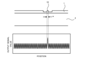
- 1 is a diagram (top) showing the shapes of the thin plate and cladding layer at the end face of an optical waveguide element, and a graph (bottom) explaining the state of the output signal value of monitor light at the position of input light.
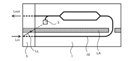
- FIG. 1 is a plan view illustrating an optical waveguide element according to the present invention. 1 is a diagram (top) showing the shapes of a thin plate, a cladding layer and an optical absorber at an end face of an optical waveguide element of the present invention, and a graph (bottom) explaining the state of an output signal value of a monitor light at the position of an input light.
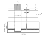
- FIG. 1 is a plan view illustrating a conventional optical waveguide element. 1 is a diagram (top) showing the shapes of the thin plate and cladding layer at the end face of an optical waveguide element, and a graph (bottom) explaining the state of the output signal value of monitor light at the position of an input light.
- FIG. 2 is a diagram for explaining the arrangement position of a light absorber in the optical waveguide element of the present invention.
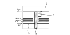
- 1A and 1B are diagrams illustrating a state in which a plurality of optical absorbers are arranged to sandwich an optical waveguide in the optical waveguide element of the present invention.
- 1A to 1C are diagrams illustrating an example in which a plurality of optical absorbers are arranged on one side of an optical waveguide in an optical waveguide element of the present invention.
- FIG. 8 is a diagram showing an application example of the embodiment of FIG. 7.
- 1A to 1C are diagrams illustrating an example in which an optical absorber is disposed within a cladding layer in the optical waveguide element of the present invention.
- FIGS. 1A to 1C are diagrams illustrating an example in which a pseudo waveguide is used in the optical waveguide element of the present invention.
- FIG. 11 is a diagram showing an application example of the embodiment of FIG. 10.
- 1A to 1C are diagrams illustrating an example in which electrodes are also used as part of a light absorbing means in the optical waveguide element of the present invention.
- 10A and 10B are plan views showing other optical waveguide shapes that can be used in the optical waveguide element of the present invention.
- 1 is a plan view showing an optical modulation device and an optical transmission device according to the present invention;
- the present invention is an optical waveguide element having a thin plate 1 on which an optical waveguide 10 is formed and an optical waveguide substrate having a cladding layer 2 arranged in contact with the lower surface of the thin plate, the optical waveguide is characterized in that the optical input section and the optical output section of the optical waveguide are arranged on the same side surface of the optical waveguide substrate, and a light absorber LA is provided between the optical input section and the optical output section and has an exposed portion exposed on the side surface.
- the light absorber LA extends so as to interrupt the straight line connecting the optical input section and the light receiving element 3, so that it is possible to suppress the leakage light LL from the optical input section from being coupled to the light receiving element. Furthermore, by arranging the light absorber also at the end of the substrate opposite to the end of the substrate where the optical input section is located, it is possible to further suppress the coupling of the leakage light from the optical waveguide to the light receiving element 3 and the folded waveguide.
- the thin plate 1 can be made of a variety of materials, including substrates with electro-optical effects such as lithium niobate (LN), lithium tantalate (LT), and PLZT (lead lanthanum zirconate titanate), vapor-grown films made from these materials, and even semiconductor and organic materials.
- substrates with electro-optical effects such as lithium niobate (LN), lithium tantalate (LT), and PLZT (lead lanthanum zirconate titanate), vapor-grown films made from these materials, and even semiconductor and organic materials.
- an optical waveguide As a method of forming an optical waveguide, it is possible to use a rib-type optical waveguide or a slot waveguide, in which the part of the substrate that corresponds to the optical waveguide is made convex by etching the surface of the substrate other than the optical waveguide and forming grooves on both sides of the optical waveguide.
- a convex waveguide with a width w or height of about 1 ⁇ m that provides strong light confinement is used.
- the thin plate on which the optical waveguide is formed is thinned by grinding and polishing to a thickness of 10 ⁇ m or less, more preferably 5 ⁇ m or less, and even more preferably less than 1 ⁇ m (the lower limit of the thickness is preferably 0.3 ⁇ m or more), or a thin-film substrate is produced using the smart cut method (a method of thinning by ion implantation peeling).
- the height of the rib-type optical waveguide or slot waveguide is preferably set to 1 ⁇ m or less in the direction perpendicular to the interface between the cladding layer and the optical waveguide substrate. It is also possible to form a vapor-grown film on another substrate to about the thickness of the substrate described above, and process the film into the shape of the optical waveguide described above.
- the thin plate 1 on which the optical waveguide is formed is adhesively fixed to a holding substrate (not shown) via an intermediate clad layer 2.
- a substrate formed by integrating the thin plate 1, the clad layer 2, and the holding substrate is called an "optical waveguide substrate.”
- the support substrate can be made of silicon (Si) of 1 mm or less, crystal such as alpha quartz single crystal having a low dielectric constant, glass material, sapphire, or the like.
- a material with a lower refractive index than the thin plate 1 is used for the cladding layer 2.
- a material with a thermal expansion coefficient close to that of the thin plate 1 is used.
- a Si oxide film such as SiO2, SiN, Al2O3 , MgF, La2O3 , ZnO, MgO, CaF2 , Y2O3 , or the like is used with a thickness of 10 ⁇ m or less.
- the optical waveguide element of the present invention is characterized in that, as shown in Fig. 3, the optical input section and the optical output section of the optical waveguide 10 are arranged on the same side (left side of the figure) of the optical waveguide substrate (thin plate 1), and an optical absorber LA is provided between the optical input section and the optical output section and has an exposed portion exposed on the side.
- the optical absorber LA does not need to be arranged at the location where the optical waveguide 10 and the optical absorber LA intersect, and a non-optical absorber such as a material usable for the cladding layer 2, such as SiO2, or a permanent resist may be arranged between the optical waveguide 10 and the optical absorber LA to reduce absorption of the light waves propagating through the optical waveguide 10.
- This optical absorber LA suppresses the leakage light LL leaking from the optical input section from entering the optical output section or the light receiving element 3, thereby increasing the extinction ratio of the signal light and suppressing the noise of the light receiving element.
- the meaning of the "light absorber" in the present invention does not only mean a state in which the end face of the light absorber is disposed on the end face of the optical waveguide substrate, like the end face of the optical waveguide, as shown in Fig. 4.
- the end face of the light absorber is slightly recessed from the end face of the optical waveguide substrate toward the inside of the substrate, it is understood to be an “exposed portion” if the end face of the light absorber suppresses the intrusion of light input from outside the substrate.
- the recess distance of the end face of the light absorber is preferably 10 ⁇ m or less, taking into consideration the absorption of light.
- the light absorber LA Since the light absorber LA is exposed from the side of the optical waveguide substrate, as shown in the lower graph of Figure 4, when input light is irradiated at the position of the light absorber LA, the light intensity of the output light Lout and the output signal value of the light receiving element 3 are lower than other signal levels. As a result, by monitoring the output signal value, it is easy to determine which position the input light is irradiated at, and the position of the optical waveguide 10 can be easily determined.
- the shape of the end of the light absorber does not need to be rectangular as shown in the upper diagram of FIG. 4, but it is desirable to make it a shape and size that fully includes the mode field diameter (MFD) of the light input/output end.
- MFD mode field diameter
- the light absorber LA a structure larger than the light guide 10
- the visibility of the light absorber is ensured when the light guide element is viewed in a plan view, and at the same time, it becomes easier to estimate the position of the light guide.
- the width w of the light guide is about 1 ⁇ m
- the width w1 of the light absorber needs to be 1 ⁇ m or more.
- the size of the exposed part of the light absorber is set larger than the mode field diameter.
- the light absorber LA As described above, by arranging the light absorber at the light input/output end, it can be used as an alignment mark during assembly and as a structure for improving the extinction ratio after assembly.
- the material used for the light absorber LA is not particularly limited as long as it is a material that can absorb light, but for example, metals (Nb, Ti, Ni, Au, Si, Al, Cu, Cr, etc.) and carbon black can be used.
- metals Nb, Ti, Ni, Au, Si, Al, Cu, Cr, etc.
- carbon black carbon black
- the distance g1 from the center of the MFD at the input/output end of the optical waveguide 10 to the light absorber is preferably 0.75 times or more the mode field diameter of the light input part and shorter than the distance g2 between the light absorber LA and the light output part.
- the distance g1 is large, it becomes difficult to specify the position of the optical waveguide 10, so it is more preferable to set the distance g1 to 10 ⁇ m or less.
- the circular symbols under Lin and Lout indicate the propagation direction of the light wave, with Lin indicating that the light wave propagates into the drawing, and Lout indicating that the light wave propagates towards the front of the drawing.
- the exposed portion of the light absorber is composed of a plurality of separate light absorbers.
- the optical absorbers (LA1, LA2) are arranged so as to sandwich the optical waveguide 10, so that the position of the optical waveguide 10 can be more easily specified.
- Figs. 7 and 8 it is possible to arrange a plurality of optical absorbers on one side of the optical waveguide 10.
- the size of the end of the optical absorber is set to 1 to 3 times the MFD size of the optical input section, and as shown in Fig. 7, absorbers of the same size may be arranged at equal intervals, or as shown in Fig. 8, the size of the end of the optical absorber may be simply increased (decreased).
- Fig. 8 shows an arrangement in which the optical absorbers become smaller as they approach the optical input waveguide.
- the volume of the light absorbers increases, and the light absorption effect is also improved.
- the width of the light absorber the time when the output of the light receiving element is turned off (width of the light absorber) changes, so it becomes easier to identify the current position of the optical member and the direction of the optical waveguide 10 than by arranging multiple light absorbers of the same size.
- the side of the optical absorber LA that is closest to the optical waveguide 10 is separated from the thin plate 1 and the cladding layer 2, but leaking light can be absorbed more reliably if these are in contact with each other.
- the light absorber LA is placed on the clad layer 2, and in Figs. 7 and 8, a groove is machined in the clad layer 2 and the light absorber LA is placed in it. Furthermore, in Fig. 9, the light absorber LA is placed so as to fill the groove formed in the clad layer 2, and by placing the light absorber LA in close contact with the thin plate 1 and the clad layer 2, the light absorber can be fixed more firmly. Moreover, by placing the light absorber in the clad layer as shown in Figs. 7 to 9, the leaked light leaked into the clad layer 2 can be absorbed more reliably.
- the depth to which the light absorber penetrates the clad layer is set to a range of 1/2 or less of the thickness of the clad layer. For example, when the clad layer thickness is 2 ⁇ m, the depth to which the light absorber penetrates the clad layer is set to a range of 0 ⁇ m to 1 ⁇ m.
- FIG. 10 and 11 show an embodiment using a pseudo-waveguide DW.
- the light absorber is disposed so as to penetrate into the cladding layer at multiple points, a part of the thin plate (DW) remains as shown in Fig. 10. It is possible to avoid forming the remaining part of the thin plate as shown in Fig. 5, but by using this remaining part as a pseudo-waveguide DW, it becomes possible to absorb leaked light more effectively.
- a pseudo-waveguide DW with the same height as the optical waveguide and width w2 is formed between the optical absorbers LA1 and LA2. Furthermore, in FIG. 11, the optical absorber LA is arranged so as to cover the pseudo-waveguide DW.
- the effect of capturing the leaking light is improved. Even the leaking light that cannot be completely absorbed by the optical absorber can be guided to the pseudo-waveguide, and the optical absorber arranged in contact with the pseudo-waveguide DW can effectively absorb the leaking light propagating through the pseudo-waveguide.
- the light absorption effect can be improved by separately arranging an optical absorber or an electrode (described later) on part of the upper surface of the pseudo-waveguide DW in FIG. 10.
- the cross-sectional area of the pseudo-waveguide DW is equal to or larger than the area of the mode field diameter of the optical input portion of the optical waveguide 10, and is equal to or smaller than four times the area of the mode field diameter. If the cross-sectional area of the pseudo-waveguide DW is made too large, the leaked light is diffused, and not only the effect of capturing the leaked light is reduced, but also the amount of the leaked light absorbed by the optical absorber is reduced. Furthermore, as shown in FIG. 11, if there are projections and recesses below the light absorber LA, this helps prevent the light absorber from peeling off due to an anchor effect.
- leakage light propagates through the pseudo-waveguide DW and is absorbed, so it is more preferable to make the length of the light absorber LA in the pseudo-waveguide DW direction (depth direction in the drawing) greater than the width of the light absorber LA.
- the light absorption function not only of the light absorber but also of a part M of the electrode arranged on the thin plate 1.
- an electrode M for example, on the upper surface of the pseudo-waveguide DW in FIG. 10 or on the extension line of the pseudo-waveguide, the leaked light propagating through the pseudo-waveguide can be absorbed by the electrode M.
- the light absorber LA1, LA2
- the light absorber and the electrode are arranged in a replaced manner as shown in FIG. 12 to avoid a short circuit with the electrode M.
- the light absorber LA extends to the end of the substrate (near the light input section), it is also possible to suppress the leaked light LL from the light input section from being directly received by the PD. Furthermore, by providing a pseudo-waveguide DW as shown in FIG. 10 and arranging light absorbers LA1 and LA2 on both sides of it, the light propagating through the pseudo-waveguide can be absorbed in the longitudinal direction of the light absorbers LA1 and LA2, further suppressing the coupling of the leaked light LL to the light receiving element 3.
- the optical waveguide 10 of the optical waveguide element is folded once, but it is not limited to this, and it is also possible to fold it three or more times as shown in FIG. 13.
- the optical absorber LA extends so as to block the straight line connecting the optical input section and the light receiving element 3, so that it is possible to suppress the leakage light LL from the optical input section from coupling to the light receiving element.
- the optical absorber at the end of the substrate opposite to the end of the substrate where the optical input section is located, it is possible to further suppress the coupling of the leakage light LL to the light receiving element 3 and the folded waveguide.
- the optical member used in the optical waveguide element of the present invention is not limited to the lens array as shown in FIG.
- a rib-type optical waveguide formed of an LN thin plate is illustrated as the shape of the optical waveguide at the chip end of the optical waveguide substrate, but it goes without saying that the present invention can also be applied in the same way when a spot size conversion section is formed at the end of the optical waveguide.
- a compact optical modulation device MD can be provided by housing the optical waveguide element (thin plate 1) of the present invention in a housing CA made of metal or the like and connecting the outside of the housing to the optical waveguide element with an optical fiber F.
- a collimator lens LN is disposed at the tip of the optical fiber F, and light waves are input and output between the optical waveguide 10 and the optical waveguide 10 via a lens array 6 disposed on the side of the optical waveguide element.
- the reference numeral 5 denotes a reinforcing member superimposed on the substrate 1 along the end face of the substrate 1, and is used when directly joining an optical component such as an optical fiber to the end face of the substrate 1.
- An electronic circuit that outputs a modulation signal S0 that causes the optical modulation device MD to perform a modulation operation can be connected to the optical modulation device MD to configure an optical transmission device OTA. Since the modulation signal S to be applied to the optical waveguide element needs to be amplified, a driver circuit DRV is used.
- the driver circuit DRV and the digital signal processor DSP can be placed outside the housing CA, but can also be placed inside the housing CA. In particular, by placing the driver circuit DRV inside the housing, the propagation loss of the modulation signal from the driver circuit can be further reduced and a wider bandwidth can be achieved.
- an optical waveguide element having an optical waveguide substrate in which a clad layer is disposed on the underside of a thin plate on which an optical waveguide is formed, which suppresses deterioration of the extinction ratio and the complication of alignment work with optical components.
- an optical modulation device and an optical transmission device using an optical waveguide element having such excellent effects.
Landscapes
- Physics & Mathematics (AREA)
- Engineering & Computer Science (AREA)
- Microelectronics & Electronic Packaging (AREA)
- General Physics & Mathematics (AREA)
- Optics & Photonics (AREA)
- Optical Integrated Circuits (AREA)
Abstract
本発明の目的は、光導波路を形成した薄板の下面にクラッド層を配置した光導波路基板を有する光導波路素子において、消光比の劣化や光学部材との位置合わせ作業の煩雑化を抑制した光導波路素子を提供することである。 本発明は、光導波路(10)を形成した薄板(1)と、該薄板の下面に接してクラッド層(2)を配置した光導波路基板を有する光導波路素子において、該光導波路は、該光導波路の光入力部と光出力部とが、該光導波路基板の同じ側面に配置されており、該光入力部と該光出力部との間に配置され、該側面に露出する露出部分を有する光吸収体(LA)を設けたことを特徴とする。
Description
本発明は、光導波路素子とそれを用いた光変調デバイス並びに光送信装置に関し、特に、光導波路を形成した薄板と、該薄板の下面に接してクラッド層を配置した光導波路基板を有する光導波路素子に関する。
光通信分野や光計測分野において、ニオブ酸リチウム(LN)などの電気光学効果を有する基板に光導波路を形成し、光導波路を伝搬する光波を変調する変調電極を備えた光変調器などの光導波路素子が多用されている。
HB-CDM(High Bandwidth Coherent Driver Modulator)のようなドライバ集積型変調器では、光導波路素子を駆動するドライバ回路を光導波路素子と一緒に筐体内に組み込み、さらに全体のパッケージを小型化することなどが求められている。このため、光導波路素子自体も小型化し、1μm程度の幅や高さを有するリブ型光導波路を形成した薄板が利用されている。光導波路を形成する薄板の機械的強度を高め、また、光導波路による光閉じ込め強度を高め、さらには、光波とマイクロ波との速度整合を図るため、薄板と保持基板との間にクラッド層を配置した光導波路基板が利用されている。
また、光導波路の形状や配置としては、図1に示すように、光導波路基板の同一側面に光導波路の光入力部と光出力部を配置した、所謂、折り返し構造も採用されている。このため、光導波路10に入射する入力光Linの一部が漏れ光LLとなって、薄板やクラッド層を伝搬し、光出力部に漏れ光が混入し、信号光の消光比が劣化するなどの原因となっている。また、信号光をモニタする受光素子3に漏れ光LLが入射し、モニタ精度が低下するなどの不具合も生じていた。
光導波路以外を伝搬する漏れ光などの迷光を除去する方法として、特許文献1では基板の上に配置した金属膜などで迷光を吸収する方法が提案されている。しかしながら、薄板1を用いた光導波路素子では、図2の上側に示すように、薄板1の下には、薄板よりも厚みの大きいクラッド層2が存在しており、このクラッド層2を伝搬する漏れ光まで吸収や除去するには、不十分であった。
光変調器において、光導波路素子(薄板1)に取り付けるレンズ等の光学部材6の位置は光変調器の特性に大きく影響する。近年開発されている小型の光変調器は、光導波路幅が1μm以下と従来の光変調器に比べて1/10以下と極めて小さくなっており、光導波路自体の視認性が悪い。さらに光導波路素子の端部では、薄板上に補強部材5を貼り合わせる構造を採用しており、光導波路10の視認性の悪さはより顕著となり、光導波路素子と光学部材との位置合わせを難しくしている。
図1のように、薄板1を含む光導波路基板と光学部材6などを位置合わせする際には、光入力部に光波を入力し、出力光Loutをモニタしながら光学部材の位置を調整している。小型の光変調器では、光入出力部が光導波路基板の同じ一辺にあるため、光学部材のアライメントには光の出射光のみでなく、受光素子3も併用しての光学部材の位置合わせが有効である。しかしながら、入力光の漏れ光が受光素子に直接結合してノイズとなり、図2の下側に示すグラフのように、入力光の入射位置が変化しても受光素子の出力信号値には多くのノイズが存在する。その結果、光導波路幅wが1μm以下の場合には、光学部材の位置合わせの難易度は極めて高くなる。
本発明が解決しようとする課題は、上述したような問題を解決し、光導波路を形成した薄板の下面にクラッド層を配置した光導波路基板を有する光導波路素子において、消光比の劣化や光学部材との位置合わせ作業の煩雑化を抑制した光導波路素子を提供することである。また、この光導波路素子を用いた光変調デバイス及び光送信装置を提供することである。
上記課題を解決するため、本発明の光導波路素子、光変調デバイス、及び光送信装置は、以下のような技術的特徴を有する。
(1) 光導波路を形成した薄板と、該薄板の下面に接してクラッド層を配置した光導波路基板を有する光導波路素子において、該光導波路は、該光導波路の光入力部と光出力部とが、該光導波路基板の同じ側面に配置されており、該光入力部と該光出力部との間に配置され、該側面に露出する露出部分を有する光吸収体を設けたことを特徴とする。
(1) 光導波路を形成した薄板と、該薄板の下面に接してクラッド層を配置した光導波路基板を有する光導波路素子において、該光導波路は、該光導波路の光入力部と光出力部とが、該光導波路基板の同じ側面に配置されており、該光入力部と該光出力部との間に配置され、該側面に露出する露出部分を有する光吸収体を設けたことを特徴とする。
(2) 上記(1)に記載の光導波路素子において、該光吸収体の前記露出部分の大きさは、該光入力部のモードフィールド径よりも大きいことを特徴とする。
(3) 上記(1)に記載の光導波路素子において、該光吸収体の前記露出部分は、複数の分離した光吸収体で構成されていることを特徴とする。
(4) 上記(1)に記載の光導波路素子において、該光吸収体は該クラッド層に入り込むように配置されていることを特徴とする。
(5) 上記(4)に記載の光導波路素子において、該光入力部と該光出力部との間で、該光吸収体が配置される範囲の内側には、該薄板の一部で疑似導波路が形成されていることを特徴とする。
(6) 上記(5)に記載の光導波路素子において、該疑似導波路の断面積は、該光入力部のモードフィールド径の面積以上であり、該モードフィールド径の面積の4倍以下であることを特徴とする。
(7) 上記(1)に記載の光導波路素子において、該光吸収体と該光入力部との距離は、該光入力部のモードフィールド径の0.75倍以上であり、該光吸収体と該光出力部との距離よりも短いことを特徴とする。
(8) 上記(1)乃至(7)のいずれかに記載の光導波路素子と、該光導波路素子を収容する筐体と、該光導波路素子に光波を入出力する光ファイバとを有することを特徴とする光変調デバイスである。
(9) 上記(8)に記載の光変調デバイスにおいて、該光導波路を伝搬する光波を変調する変調電極を該基板に設け、該変調電極に入力する変調信号を増幅する電子回路を該筐体の内部又は外部に有することを特徴とする。
(10) 上記(9)に記載の光変調デバイスと、該光変調デバイスに変調動作を行わせる変調信号を出力する電子回路とを有することを特徴とする光送信装置である。
本発明により、光導波路を形成した薄板と、該薄板の下面に接してクラッド層を配置した光導波路基板を有する光導波路素子において、該光導波路は、該光導波路の光入力部と光出力部とが、該光導波路基板の同じ側面に配置されており、該光入力部と該光出力部との間に配置され、該側面に露出する露出部分を有する光吸収体を設けたため、光入力部の漏れ光が光出力部に混入することを抑制でき、信号光の消光比の劣化を抑制することが可能となる。しかも、光学部材の位置合わせに使用する入力光(モニタ光)が、光吸収体の露出部分に照射された際には、モニタ信号の低下が発生し、入力光を光導波路の光入力部に容易に位置合わせすることが可能となり、光学部材の位置合わせ作業を円滑に行うことが可能となる。また、この優れた効果を奏する光導波路素子を用いた光変調デバイス及び光送信装置も提供することが可能となる。
以下、本発明について好適例を用いて詳細に説明する。
本発明は、図3及び4に示すように、光導波路10を形成した薄板1と、該薄板の下面に接してクラッド層2を配置した光導波路基板を有する光導波路素子において、該光導波路は、該光導波路の光入力部と光出力部とが、該光導波路基板の同じ側面に配置されており、該光入力部と該光出力部との間に配置され、該側面に露出する露出部分を有する光吸収体LAを設けたことを特徴とする。光吸収体LAは、光入力部と受光素子3を結ぶ直線を遮るように延伸しているため、光入力部からの漏れ光LLが受光素子に結合することを抑制できる。さらに、光吸収体を、光入力部のある基板端部の反対側にある基板端部にも配置することで、受光素子3や折り返し導波路への光導波路からの漏れ光の結合をより抑制することが可能である。
本発明は、図3及び4に示すように、光導波路10を形成した薄板1と、該薄板の下面に接してクラッド層2を配置した光導波路基板を有する光導波路素子において、該光導波路は、該光導波路の光入力部と光出力部とが、該光導波路基板の同じ側面に配置されており、該光入力部と該光出力部との間に配置され、該側面に露出する露出部分を有する光吸収体LAを設けたことを特徴とする。光吸収体LAは、光入力部と受光素子3を結ぶ直線を遮るように延伸しているため、光入力部からの漏れ光LLが受光素子に結合することを抑制できる。さらに、光吸収体を、光入力部のある基板端部の反対側にある基板端部にも配置することで、受光素子3や折り返し導波路への光導波路からの漏れ光の結合をより抑制することが可能である。
薄板1としては、ニオブ酸リチウム(LN)やタンタル酸リチウム(LT)、PLZT(ジルコン酸チタン酸鉛ランタン)などの電気光学効果を有する基板や、これらの材料による気相成長膜、さらには、半導体材料や有機材料など種々の材料も利用可能である。
光導波路の形成方法としては、光導波路以外の基板表面をエッチングし、光導波路の両側に溝を形成するなど、基板の光導波路に対応する部分を凸状としたリブ型光導波路やスロット導波路を利用することが可能である。特に、光導波路素子自体を小型化する場合や折り曲げた光導波路を使用する場合などには、光閉じ込めの強い、幅w又は高さが1μm程度の凸状導波路を用いる。
光導波路を形成した薄板は、変調信号のマイクロ波と光波との速度整合を図るため、10μm以下、より好ましくは5μm以下、更に好ましくは1μm未満の厚さ(厚さの下限は0.3μm以上が好ましい)まで研削研磨により薄板化する方法と、スマートカット法(イオン注入剥離により薄膜化する方法)を用いて薄膜化基板を作製する。リブ型光導波路やスロット導波路の高さは、クラッド層と光導波路基板の界面から垂直な方向に、1μm以下に設定することが好ましい。また、他の基板上に気相成長膜を上述の基板の厚さ程度で形成し、当該膜を上述のような光導波路の形状に加工することも可能である。
光導波路を形成した薄板1は、機械的強度を高めるため、中間層となるクラッド層2を介して、保持基板(不図示)に接着固定される。本発明では、薄板1、クラッド層2及び保持基板を一体化した基板を「光導波路基板」という。
保持基板には、1mm以下のシリコン(Si)や誘電率の低いアルファ石英単結晶等の水晶やガラス材、サファイア等が利用可能である。
また、クラッド層2には、光波と電気信号(マイクロ波)との速度整合を図るため、薄板1よりも屈折率の低い材料が使用される。また、薄板1に熱応力が加わるのを抑制するため、熱膨張率が薄板1に近い材料を使用する。具体的には、SiO2などのSi酸化膜やSiN、Al2O3、MgF、La2O3、ZnO、MgO,CaF2,Y2O3などを厚さ10μm以下で用いる。
保持基板には、1mm以下のシリコン(Si)や誘電率の低いアルファ石英単結晶等の水晶やガラス材、サファイア等が利用可能である。
また、クラッド層2には、光波と電気信号(マイクロ波)との速度整合を図るため、薄板1よりも屈折率の低い材料が使用される。また、薄板1に熱応力が加わるのを抑制するため、熱膨張率が薄板1に近い材料を使用する。具体的には、SiO2などのSi酸化膜やSiN、Al2O3、MgF、La2O3、ZnO、MgO,CaF2,Y2O3などを厚さ10μm以下で用いる。
本発明の光導波路素子の特徴は、図3に示すように、光導波路10は、該光導波路の光入力部と光出力部とが、光導波路基板(薄板1)の同じ側面(図の左側)に配置されており、該光入力部と該光出力部との間に配置され、該側面に露出する露出部分を有する光吸収体LAを設けたことである。光導波路10と光吸収体LAとが交差する場所には、光吸収体LAを配置しなくてもよいし、光導波路10と光吸収体LAとの間にSiO2などクラッド層2に使用可能な材料や永久レジストなどの非光吸収体を配して光導波路10を伝搬する光波の吸収を低減する構成としてもよい。この光吸収体LAにより、光入力部から漏れた漏れ光LLが光出力部や受光素子3に入射することが抑制され、信号光の消光比を高め、受光素子のノイズを抑制することが可能となる。
また、本発明における「光吸収体」が「(光導波路基板の)側面に露出する露出部分を有する」ことの意味は、図4に示すように、光導波路基板の端面において、光導波路の端面と同様に、光吸収体の端面が配置されている状態だけを意味しているのではない。例えば、光吸収体の端面が光導波路基板の端面から基板の内側に若干後退していても、基板外部から入力される光に対し、光吸収体の端面で該光の侵入が抑制されている場合には、「露出部分」と解される。
なお、光吸収体の端面の後退距離は光の吸収を考慮すると10μm以下が好ましい。
なお、光吸収体の端面の後退距離は光の吸収を考慮すると10μm以下が好ましい。
光吸収体LAが光導波路基板の側面から露出しているため、図4の下側のグラフに示すように、光吸収体LAの位置に入力光を照射した場合には、出力光Loutの光強度や受光素子3の出力信号値は他の信号レベルと比較し低くなる。これにより、出力信号値をモニタすることで、入力光がどの位置に照射されているのかを容易に判断でき、光導波路10の位置を容易に判定することが可能となる。
光吸収体の端部の形状は図4の上側の図に示すように、矩形である必要はないが、光入出力端部のモードフィールド径(MFD)が十分に包含される形状・大きさにすることが望ましい。また、光吸収体LAを光導波路10よりも大きい構造物にすることで、光導波路素子を平面視した際に光吸収体の視認性が確保され、同時に光導波路の位置の推定も容易になる。光吸収体に照射された光を十分に吸収又は基板内に侵入するのを抑制するためには、光導波路の幅wよりも光吸収体LAの幅w1をより広くとることが必要であり、例えば、光導波路幅wが1μm程度の場合は、光吸収体の幅w1は1μm以上は必要となる。また、光導波路の光入力部のモードフィールド径(MFD)に着目した場合には、光吸収体の露出部分の大きさは、該モードフィールド径よりも大きく設定することが必要である。光吸収体の端部における大きさをMFDが包含できる大きさと規定することで、光学部材のアライメント時に確実に光が吸収でき、受光素子などの出力を0に近づけることが可能となる。
以上のように、光吸収体を光入出力端部に配置することで組立時のアライメントマークとして、また、組立後の消光比を改善する構造として使用できる。
光吸収体LAに使用する材料としては、光を吸収できる材料であれば、特に限定されないが、例えば、金属(Nb,Ti,Ni,Au,Si,Al,Cu,Cr等)や、カーボンブラックなどを用いることができる。
図4では、薄板1に溝加工を行い、光吸収体LAをクラッド層2上に接して配置しているが、後述するように、クラッド層2に入り込むように光吸収体を配置してもよい。
光吸収体LAに使用する材料としては、光を吸収できる材料であれば、特に限定されないが、例えば、金属(Nb,Ti,Ni,Au,Si,Al,Cu,Cr等)や、カーボンブラックなどを用いることができる。
図4では、薄板1に溝加工を行い、光吸収体LAをクラッド層2上に接して配置しているが、後述するように、クラッド層2に入り込むように光吸収体を配置してもよい。
以下では、光吸収体を用いた様々な実施例について説明する。
光吸収体LAは光導波路10の光入力部に近いほど、漏れ光がLNなどの薄板内やクラッド層内を拡散しにくくなり、光吸収効果が高まるため、可能な限り光入力部に近い方が望ましい。図5に示すように、光吸収体LAは光導波路10の入出力端部のMFDの中心から光吸収体までの距離g1は、光入力部のモードフィールド径の0.75倍以上であり、光吸収体LAと光出力部との距離g2よりも短いことが好ましい。また、距離g1が大きくなると、光導波路10の位置を特定する作業が難しくなるため、距離g1を10μm以下に設定することがより好ましい。
図5における、Lin、Loutの下の丸の符号は、光波の伝搬方向を示し、Linは図面の奥方向に、Loutは図面の表方向に光波が伝搬すること意味している。以下の図面も同様である。
光吸収体LAは光導波路10の光入力部に近いほど、漏れ光がLNなどの薄板内やクラッド層内を拡散しにくくなり、光吸収効果が高まるため、可能な限り光入力部に近い方が望ましい。図5に示すように、光吸収体LAは光導波路10の入出力端部のMFDの中心から光吸収体までの距離g1は、光入力部のモードフィールド径の0.75倍以上であり、光吸収体LAと光出力部との距離g2よりも短いことが好ましい。また、距離g1が大きくなると、光導波路10の位置を特定する作業が難しくなるため、距離g1を10μm以下に設定することがより好ましい。
図5における、Lin、Loutの下の丸の符号は、光波の伝搬方向を示し、Linは図面の奥方向に、Loutは図面の表方向に光波が伝搬すること意味している。以下の図面も同様である。
図6乃至図8は、複数の光吸収体を配置したものである。特に、光吸収体の露出部分は、複数の分離した光吸収体で構成されている。
図6では、光導波路10を挟むように光吸収体(LA1,LA2)を配置することで、光導波路10の位置をより特定し易くなる。また、図7及び8に示すように、光導波路10の片側に複数の光吸収体を配置することも可能である。光吸収体の端部における大きさは光入力部のMFDサイズの1~3倍に設定され、図7に示すように、同じ大きさの吸収体を等間隔で配置してもよいし、図8に示すように、光吸収体の端部の大きさが単純増加(減少)するように配置してもよい。図8では、光吸収体が光入力導波路に近づくにつれ小さくなるように配置している図を示している。
図6では、光導波路10を挟むように光吸収体(LA1,LA2)を配置することで、光導波路10の位置をより特定し易くなる。また、図7及び8に示すように、光導波路10の片側に複数の光吸収体を配置することも可能である。光吸収体の端部における大きさは光入力部のMFDサイズの1~3倍に設定され、図7に示すように、同じ大きさの吸収体を等間隔で配置してもよいし、図8に示すように、光吸収体の端部の大きさが単純増加(減少)するように配置してもよい。図8では、光吸収体が光入力導波路に近づくにつれ小さくなるように配置している図を示している。
光吸収体を複数配置することで、光吸収体の体積が増え、光吸収効果もより高くなる。アライメント時には、受光素子の出力のON/OFFを繰り返す回数・時間(光吸収体の幅や距離)から、光学部材の現在位置を確認することが容易となる。また、光吸収体の幅を変化させることで、受光素子の出力がOFFになる時間(光吸収体の幅)が変化するので、同じ大きさの光吸収体を複数配置するよりも、光学部材の現在位置や光導波路10のある方向をより特定し易くなる。
なお、図7や図8では複数の光吸収体LAのうち光導波路10に最も近い光吸収体LAの側面が薄板1やクラッド層2から乖離しているが、これらは接触させた方が漏れ光をより確実に吸収することができる。
なお、図7や図8では複数の光吸収体LAのうち光導波路10に最も近い光吸収体LAの側面が薄板1やクラッド層2から乖離しているが、これらは接触させた方が漏れ光をより確実に吸収することができる。
図5及び6では、クラッド層2の上に光吸収体LAを配置し、図7及び8では、クラッド層2に溝を加工し、その中に光吸収体LAを配置している。さらに、図9では、クラッド層2に形成した溝を満たすように光吸収体LAを配置しており、薄板1やクラッド層2と密着させて光吸収体LAを配置することで、より強固に光吸収体を固定することができる。しかも、図7乃至9に示すように、クラッド層に入り込んで光吸収体を配置することで、クラッド層2内に漏れた漏れ光をより確実に吸収することができる。光吸収体がクラッド層に入り込む深さは、クラッド層の厚さの1/2以下の範囲で設定される。例えば、クラッド層厚さが2μmの場合には、光吸収体がクラッド層に入り込む深さは0μm以上1μm以下範囲で決められる。
図10及び11は、疑似導波路DWを用いた実施例を示す。
光吸収体をクラッド層内に複数個所で入り込むように配置すると、図10に示すように、薄板の一部(DW)が残存する。図5に示すように、薄板の残存部分を形成しないようにすることも可能であるが、この残存部分を疑似導波路DWとして利用することで、漏れ光をより効果的に吸収することが可能となる。
光吸収体をクラッド層内に複数個所で入り込むように配置すると、図10に示すように、薄板の一部(DW)が残存する。図5に示すように、薄板の残存部分を形成しないようにすることも可能であるが、この残存部分を疑似導波路DWとして利用することで、漏れ光をより効果的に吸収することが可能となる。
図10では、光吸収体LA1とLA2との間に、高さは光導波路と同じで幅がw2の疑似導波路DWが形成されている。さらに、図11では、疑似導波路DWを覆うように光吸収体LAが配置されている。漏れ光が結合するような疑似導波路DWを光吸収体の間や光吸収体の下に配置することで、漏れ光の捕捉効果を高めている。光吸収体で完全に吸収できなかった漏れ光も、疑似導波路に誘導することで、疑似導波路DWに接触して配置された光吸収体により、疑似導波路を伝搬する漏れ光を効果的に吸収することが可能となる。また、図10の疑似導波路DWの上面の一部に、別途、光吸収体や後述する電極等を配置することで、光吸収効果を高めることも可能である。
疑似導波路DWの断面積は、光導波路10の光入力部のモードフィールド径の面積以上であり、該モードフィールド径の面積の4倍以下である。疑似導波路DWの断面積を大きくし過ぎると、漏れ光が拡散し、漏れ光の補足効果が低下するだけでなく、光吸収体に吸収される漏れ光の量も減少する。
また、図11のように、光吸収体LAの下に凹凸があれば、アンカー効果により、光吸収体の剥離防止にも役立つ。
図11や図12の構成は疑似導波路DWを漏れ光が伝搬することで吸収されるため、光吸収体LAの幅よりも疑似導波路DW方向(図面奥行方向)の長さの方を大きくする方がより好ましい。
また、図11のように、光吸収体LAの下に凹凸があれば、アンカー効果により、光吸収体の剥離防止にも役立つ。
図11や図12の構成は疑似導波路DWを漏れ光が伝搬することで吸収されるため、光吸収体LAの幅よりも疑似導波路DW方向(図面奥行方向)の長さの方を大きくする方がより好ましい。
さらに、図12に示すように、光吸収作用を光吸収体だけでなく、薄板1上に配置した電極の一部Mに担わせることも可能である。このような電極Mを、例えば、図10の疑似導波路DWの上面又は疑似導波路の延長線上に配置することで、疑似導波路を伝搬する漏れ光を電極Mで吸収できる。ただし、光吸収体(LA1,LA2)を金属で作成する場合には、電極Mとのショートを回避するため、図12に示すように、光吸収体と電極とは置換して配置する。この場合には、受光素子3の周囲の少なくとも一部を電極Mと光吸収体LAとで囲むことで漏れ光LLの受光素子3への結合を抑制できる。さらに光吸収体LAは、基板端部(光入力部近傍)にまで延伸しているため、光入力部からの漏れ光LLが直接PDに受光することも抑制可能である。また、図10のように疑似導波路DWを設け、その両側に光吸収体LA1、LA2を配置すると、疑似導波路を伝搬する光が、光吸収体LA1,LA2の長手方向で吸収できるため、受光素子3への漏れ光LLの結合がさらに抑制できる。
以上の説明では、光導波路素子の光導波路10を1回折り返した構造としたが、これに限らず、図13に示すように、3回以上折り返した構造100とすることも可能である。この場合にも、光吸収体LAは、光入力部と受光素子3を結ぶ直線を遮るように延伸しているため、光入力部からの漏れ光LLが受光素子に結合することを抑制できる。さらに、光吸収体を、光入力部のある基板端部の反対側にある基板端部にも配置することで、受光素子3や折り返し導波路への漏れ光LLの結合をより抑制することが可能である。また、本発明の光導波路素子に使用する光学部材は、図1のようなレンズアレイに限定されず、ファイバアレイやPLCなどの異種導波路基板にも適用可能である。さらに、光導波路基板のチップ端部における光導波路の形状として、LN薄板で形成したリブ型光導波路を図示したが、光導波路端部にスポットサイズ変換部を形成した場合も同様に、本発明が適用できることは言うまでもない。
さらに、図14に示すように、本発明の光導波路素子(薄板1)を金属等の筐体CA内に収容し、筐体の外部と光導波路素子とを光ファイバFで接続することで、コンパクトな光変調デバイスMDを提供することができる。図14では、光ファイバFの先端にコリメータレンズLNを配置し、さらに光導波路素子の側面に配置したレンズアレイ6を介して、光導波路10との間で光波の入出力を行っている。当然、空間光学系を介して光学的に接続するだけでなく、薄板1の光導波路の入出力部に光ファイバを直接接続することも可能である。なお、符号5は、基板1の端面に沿って基板1に重ね合わせた補強部材であり、光ファイバなどの光学部品を基板1の端面に直接接合する際に使用される。
光変調デバイスMDに変調動作を行わせる変調信号S0を出力する電子回路(デジタル信号プロセッサーDSP)を、光変調デバイスMDに接続することにより、光送信装置OTAを構成することが可能である。光導波路素子に印加する変調信号Sは増幅する必要があるため、ドライバ回路DRVが使用される。ドライバ回路DRVやデジタル信号プロセッサーDSPは、筐体CAの外部に配置することも可能であるが、筐体CA内に配置することも可能である。特に、ドライバ回路DRVを筐体内に配置することで、ドライバ回路からの変調信号の伝搬損失をより低減し広帯域化が可能となる。
以上のように、本発明によれば、光導波路を形成した薄板の下面にクラッド層を配置した光導波路基板を有する光導波路素子において、消光比の劣化や光学部材との位置合わせ作業の煩雑化を抑制した光導波路素子を提供することが可能となる。また、このような優れた効果を有する光導波路素子を用いた光変調デバイス及び光送信装置を提供することができる。
1 薄板
2 クラッド層
3 受光素子
10 光導波路
LA,LA1,LA2 光吸収体
2 クラッド層
3 受光素子
10 光導波路
LA,LA1,LA2 光吸収体
Claims (10)
- 光導波路を形成した薄板と、該薄板の下面に接してクラッド層を配置した光導波路基板を有する光導波路素子において、
該光導波路は、該光導波路の光入力部と光出力部とが、該光導波路基板の同じ側面に配置されており、
該光入力部と該光出力部との間に配置され、該側面に露出する露出部分を有する光吸収体を設けたことを特徴とする光導波路素子。 - 請求項1に記載の光導波路素子において、該光吸収体の前記露出部分の大きさは、該光入力部のモードフィールド径よりも大きいことを特徴とする光導波路素子。
- 請求項1に記載の光導波路素子において、該光吸収体の前記露出部分は、複数の分離した光吸収体で構成されていることを特徴とする光導波路素子。
- 請求項1に記載の光導波路素子において、該光吸収体は該クラッド層に入り込むように配置されていることを特徴とする光導波路素子。
- 請求項4に記載の光導波路素子において、該光入力部と該光出力部との間で、該光吸収体が配置される範囲の内側には、該薄板の一部で疑似導波路が形成されていることを特徴とする光導波路素子。
- 請求項5に記載の光導波路素子において、該疑似導波路の断面積は、該光入力部のモードフィールド径の面積以上であり、該モードフィールド径の面積の4倍以下であることを特徴とする光導波路素子。
- 請求項1に記載の光導波路素子において、該光吸収体と該光入力部との距離は、該光入力部のモードフィールド径の0.75倍以上であり、該光吸収体と該光出力部との距離よりも短いことを特徴とする光導波路素子。
- 請求項1乃至7のいずれかに記載の光導波路素子と、該光導波路素子を収容する筐体と、該光導波路素子に光波を入出力する光ファイバとを有することを特徴とする光変調デバイス。
- 請求項8に記載の光変調デバイスにおいて、該光導波路を伝搬する光波を変調する変調電極を該基板に設け、該変調電極に入力する変調信号を増幅する電子回路を該筐体の内部又は外部に有することを特徴とする光変調デバイス。
- 請求項9に記載の光変調デバイスと、該光変調デバイスに変調動作を行わせる変調信号を出力する電子回路とを有することを特徴とする光送信装置。
Priority Applications (1)
| Application Number | Priority Date | Filing Date | Title |
|---|---|---|---|
| PCT/JP2023/012582 WO2024201728A1 (ja) | 2023-03-28 | 2023-03-28 | 光導波路素子とそれを用いた光変調デバイス並びに光送信装置 |
Applications Claiming Priority (1)
| Application Number | Priority Date | Filing Date | Title |
|---|---|---|---|
| PCT/JP2023/012582 WO2024201728A1 (ja) | 2023-03-28 | 2023-03-28 | 光導波路素子とそれを用いた光変調デバイス並びに光送信装置 |
Publications (1)
| Publication Number | Publication Date |
|---|---|
| WO2024201728A1 true WO2024201728A1 (ja) | 2024-10-03 |
Family
ID=92904325
Family Applications (1)
| Application Number | Title | Priority Date | Filing Date |
|---|---|---|---|
| PCT/JP2023/012582 Ceased WO2024201728A1 (ja) | 2023-03-28 | 2023-03-28 | 光導波路素子とそれを用いた光変調デバイス並びに光送信装置 |
Country Status (1)
| Country | Link |
|---|---|
| WO (1) | WO2024201728A1 (ja) |
Citations (7)
| Publication number | Priority date | Publication date | Assignee | Title |
|---|---|---|---|---|
| JP2004093905A (ja) * | 2002-08-30 | 2004-03-25 | Sumitomo Osaka Cement Co Ltd | 光変調器 |
| JP2006276518A (ja) * | 2005-03-29 | 2006-10-12 | Sumitomo Osaka Cement Co Ltd | 光変調器 |
| JP2006301612A (ja) * | 2005-03-25 | 2006-11-02 | Sumitomo Osaka Cement Co Ltd | 光変調器 |
| JP2008250019A (ja) * | 2007-03-30 | 2008-10-16 | Furukawa Electric Co Ltd:The | 光集積回路および光集積回路モジュール |
| JP2014048516A (ja) * | 2012-08-31 | 2014-03-17 | Sumitomo Osaka Cement Co Ltd | 光変調器 |
| JP2022155813A (ja) * | 2021-03-31 | 2022-10-14 | 住友大阪セメント株式会社 | 光導波路素子とそれを用いた光変調デバイス並びに光送信装置 |
| JP2023008095A (ja) * | 2021-07-05 | 2023-01-19 | 富士通オプティカルコンポーネンツ株式会社 | 光デバイス及び光通信装置 |
-
2023
- 2023-03-28 WO PCT/JP2023/012582 patent/WO2024201728A1/ja not_active Ceased
Patent Citations (7)
| Publication number | Priority date | Publication date | Assignee | Title |
|---|---|---|---|---|
| JP2004093905A (ja) * | 2002-08-30 | 2004-03-25 | Sumitomo Osaka Cement Co Ltd | 光変調器 |
| JP2006301612A (ja) * | 2005-03-25 | 2006-11-02 | Sumitomo Osaka Cement Co Ltd | 光変調器 |
| JP2006276518A (ja) * | 2005-03-29 | 2006-10-12 | Sumitomo Osaka Cement Co Ltd | 光変調器 |
| JP2008250019A (ja) * | 2007-03-30 | 2008-10-16 | Furukawa Electric Co Ltd:The | 光集積回路および光集積回路モジュール |
| JP2014048516A (ja) * | 2012-08-31 | 2014-03-17 | Sumitomo Osaka Cement Co Ltd | 光変調器 |
| JP2022155813A (ja) * | 2021-03-31 | 2022-10-14 | 住友大阪セメント株式会社 | 光導波路素子とそれを用いた光変調デバイス並びに光送信装置 |
| JP2023008095A (ja) * | 2021-07-05 | 2023-01-19 | 富士通オプティカルコンポーネンツ株式会社 | 光デバイス及び光通信装置 |
Similar Documents
| Publication | Publication Date | Title |
|---|---|---|
| JP4874685B2 (ja) | 光変調器 | |
| JP5454547B2 (ja) | 光変調器 | |
| JP4658658B2 (ja) | 光変調器 | |
| JP6137023B2 (ja) | 光導波路素子 | |
| EP2624029B1 (en) | Optical waveguide element | |
| JP5012624B2 (ja) | 光導波路素子 | |
| WO2007122877A1 (ja) | 光変調素子 | |
| CN214795475U (zh) | 光波导元件、使用光波导元件的光调制器件及光发送装置 | |
| JP7666070B2 (ja) | 光導波路素子及びそれを用いた光変調デバイス並びに光送信装置 | |
| JP4183716B2 (ja) | 光導波路素子 | |
| CN101840026B (zh) | 光波导设备 | |
| JP4868763B2 (ja) | 光変調器 | |
| WO2024201728A1 (ja) | 光導波路素子とそれを用いた光変調デバイス並びに光送信装置 | |
| JP5494400B2 (ja) | 光導波路素子 | |
| CN118732154A (zh) | 光波导元件、使用光波导元件的光调制器件及光发送装置 | |
| US20260086397A1 (en) | Optical waveguide element, optical modulator, and optical transmission apparatus | |
| JP4589884B2 (ja) | 光制御素子及びその製造方法 | |
| JP2003270597A (ja) | 光可変減衰装置 | |
| JP7670153B2 (ja) | 光導波路素子及びそれを用いた光変調デバイス並びに光送信装置 | |
| WO2024166351A1 (ja) | 光導波路素子とそれを用いた光変調デバイス並びに光送信装置 | |
| US20240134117A1 (en) | Optical waveguide element, and optical transmission apparatus and optical modulation device using same | |
| JP2024107822A (ja) | 光導波路素子及びそれを用いた光変調デバイス並びに光送信装置 | |
| CN121444002A (zh) | 光波导元件、光调制器及光发送装置 | |
| CN118765382A (zh) | 光波导元件、使用光波导元件的光调制器件及光发送装置 | |
| WO2024069977A1 (ja) | 光導波路素子及びそれを用いた光変調デバイス並びに光送信装置 |
Legal Events
| Date | Code | Title | Description |
|---|---|---|---|
| 121 | Ep: the epo has been informed by wipo that ep was designated in this application |
Ref document number: 23930368 Country of ref document: EP Kind code of ref document: A1 |
|
| NENP | Non-entry into the national phase |
Ref country code: DE |
|
| 122 | Ep: pct application non-entry in european phase |
Ref document number: 23930368 Country of ref document: EP Kind code of ref document: A1 |