WO2024201683A1 - プラズマ処理装置 - Google Patents
プラズマ処理装置 Download PDFInfo
- Publication number
- WO2024201683A1 WO2024201683A1 PCT/JP2023/012352 JP2023012352W WO2024201683A1 WO 2024201683 A1 WO2024201683 A1 WO 2024201683A1 JP 2023012352 W JP2023012352 W JP 2023012352W WO 2024201683 A1 WO2024201683 A1 WO 2024201683A1
- Authority
- WO
- WIPO (PCT)
- Prior art keywords
- power supply
- heater
- film
- regions
- connector
- Prior art date
- Legal status (The legal status is an assumption and is not a legal conclusion. Google has not performed a legal analysis and makes no representation as to the accuracy of the status listed.)
- Ceased
Links
Images





Classifications
-
- H—ELECTRICITY
- H05—ELECTRIC TECHNIQUES NOT OTHERWISE PROVIDED FOR
- H05B—ELECTRIC HEATING; ELECTRIC LIGHT SOURCES NOT OTHERWISE PROVIDED FOR; CIRCUIT ARRANGEMENTS FOR ELECTRIC LIGHT SOURCES, IN GENERAL
- H05B3/00—Ohmic-resistance heating
- H05B3/20—Heating elements having extended surface area substantially in a two-dimensional [2D] plane, e.g. plate-heater
- H05B3/22—Heating elements having extended surface area substantially in a two-dimensional [2D] plane, e.g. plate-heater non-flexible
- H05B3/28—Heating elements having extended surface area substantially in a two-dimensional [2D] plane, e.g. plate-heater non-flexible heating conductor embedded in insulating material
-
- H—ELECTRICITY
- H01—ELECTRIC ELEMENTS
- H01J—ELECTRIC DISCHARGE TUBES OR DISCHARGE LAMPS
- H01J37/00—Discharge tubes with provision for introducing objects or material to be exposed to the discharge, e.g. for the purpose of examination or processing thereof
- H01J37/32—Gas-filled discharge tubes
- H01J37/32431—Constructional details of the reactor
- H01J37/32532—Electrodes
- H01J37/32577—Electrical connecting means
-
- H—ELECTRICITY
- H01—ELECTRIC ELEMENTS
- H01J—ELECTRIC DISCHARGE TUBES OR DISCHARGE LAMPS
- H01J37/00—Discharge tubes with provision for introducing objects or material to be exposed to the discharge, e.g. for the purpose of examination or processing thereof
- H01J37/32—Gas-filled discharge tubes
- H01J37/32431—Constructional details of the reactor
- H01J37/32715—Workpiece holder
- H01J37/32724—Temperature
-
- H—ELECTRICITY
- H05—ELECTRIC TECHNIQUES NOT OTHERWISE PROVIDED FOR
- H05B—ELECTRIC HEATING; ELECTRIC LIGHT SOURCES NOT OTHERWISE PROVIDED FOR; CIRCUIT ARRANGEMENTS FOR ELECTRIC LIGHT SOURCES, IN GENERAL
- H05B3/00—Ohmic-resistance heating
- H05B3/02—Details
- H05B3/03—Electrodes
-
- H—ELECTRICITY
- H10—SEMICONDUCTOR DEVICES; ELECTRIC SOLID-STATE DEVICES NOT OTHERWISE PROVIDED FOR
- H10P—GENERIC PROCESSES OR APPARATUS FOR THE MANUFACTURE OR TREATMENT OF DEVICES COVERED BY CLASS H10
- H10P50/00—Etching of wafers, substrates or parts of devices
- H10P50/20—Dry etching; Plasma etching; Reactive-ion etching
- H10P50/24—Dry etching; Plasma etching; Reactive-ion etching of semiconductor materials
- H10P50/242—Dry etching; Plasma etching; Reactive-ion etching of semiconductor materials of Group IV materials
-
- H—ELECTRICITY
- H01—ELECTRIC ELEMENTS
- H01J—ELECTRIC DISCHARGE TUBES OR DISCHARGE LAMPS
- H01J2237/00—Discharge tubes exposing object to beam, e.g. for analysis treatment, etching, imaging
- H01J2237/32—Processing objects by plasma generation
- H01J2237/33—Processing objects by plasma generation characterised by the type of processing
- H01J2237/334—Etching
Definitions
- This disclosure relates to a plasma processing apparatus in which a substrate-like sample such as a semiconductor wafer is placed on the top surface of a sample stage in a processing chamber inside a vacuum vessel, and the sample is processed using plasma formed by supplying a processing gas into the processing chamber, and in particular to a plasma processing apparatus that includes multiple film-like heaters in a dielectric film that covers the top surface of the sample stage, and that uses these heaters to adjust the temperature of the sample while processing it.
- a multi-layer film which is a multi-layer film formed on the surface of a plate-shaped sample such as a semiconductor wafer (hereinafter simply referred to as a wafer)
- adjacent films are processed vertically in the same processing chamber, without removing the wafer from the processing chamber between the processing of each of these films.
- Patent Document 1 discloses a plasma processing apparatus described as "(see claim 1) a vacuum processing apparatus having a vacuum vessel in which the inside is depressurized, a sample stage arranged in the vacuum vessel, and an electrostatic adsorption device provided on the sample stage for holding a semiconductor wafer, which generates plasma above the sample stage and etches the semiconductor wafer, the electrostatic adsorption device being a vacuum processing apparatus in which a first dielectric film is formed on a conductive substrate, a plurality of approximately ring-shaped electrode films for electrostatic adsorption are formed concentrically and spaced apart on the surface of the first dielectric film, a ring-shaped heater film is formed between the electrode films in the radial direction, and a second dielectric film is formed on the upper surface of the electrode film and the heater film.”
- the configuration of Patent Document 1 makes it possible to change the temperature distribution within the wafer surface for each etching
- Patent Document 2 discloses a plasma processing apparatus including "(see claim 1) an electrostatic chuck unit having a mounting surface on one main surface for mounting a plate-shaped sample and equipped with an electrode for electrostatic adsorption, a temperature adjustment base portion arranged on the opposite side of the electrostatic chuck unit from the mounting surface and cooling the electrostatic chuck unit, a first heater element consisting of a single or multiple main heaters that adjusts the temperature of the adsorption surface of the electrostatic chuck unit in a single or multiple main heater adjustment area, a second heater element consisting of multiple sub-heaters that adjusts the temperature of a sub-heater adjustment area that is larger than the main heater adjustment area of the first heater element, and a control unit that controls the voltage applied to the sub-heater.”
- the temperature distribution of each zone divided into multiple main heaters can be individually controlled, and the temperature adjustment in each zone divided into multiple main heaters.
- the purpose of this disclosure is to provide a technology that allows electrodes for multi-zone heater layers (heater wires) to be safely, easily, and at low cost.
- a processing chamber disposed within the vacuum vessel, the processing chamber having a wafer to be processed disposed therein and in which plasma is generated; a cylindrical sample stage disposed within the processing chamber and on whose upper surface the wafer is placed; the sample stage includes a disk-shaped substrate, a dielectric film covering an upper surface of the substrate, and a heater layer disposed inside the dielectric film; the heater layer includes a plurality of film heaters arranged in each of a plurality of rectangular regions; Each of the plurality of regions is disposed such that one side of the rectangular shape faces an adjacent region, a power supply connector having a cylindrical shape that is attached to and detached from the bottom of the base material; the power supply connector is configured to be electrically connected to one location of each of the plurality of film heaters arranged in each of the plurality of regions to supply power from a DC power source; a wiring member including a plurality of wires to which the power is supplied and made of a resin plate-like member connected to a bottom of the power supply
- This disclosure provides a plasma processing device that is safe, low-cost, and easy to manufacture.
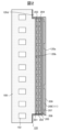
- FIG. 1 is a vertical cross-sectional view showing an outline of a configuration of a plasma processing apparatus according to an embodiment
- 2 is a cross-sectional view showing a schematic view of a part of a configuration of a sample stage of the plasma processing apparatus shown in FIG. 1
- 3 is a partially enlarged cross-sectional view showing a schematic view of a part of the configuration of the sample stage of the plasma processing apparatus shown in FIG. 2.
- FIG. 13 is a diagram showing an example of a second heater in the sample stage in the embodiment.
- FIG. 4 is a diagram showing an example of a first heater in a sample stage in the embodiment;
- FIG. 4 is a layout diagram of a power supply section and a return section of a grid heater according to an embodiment.
- FIG. 2 is a close-up view of a set of four grid heaters according to an embodiment.
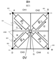
- FIG. 13 is a diagram showing an example of polarity reversal in four grid heaters and their power supply parts according to an embodiment.
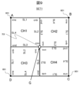
- 7 is a schematic diagram showing the relationship between the four corners (first corner cna, second corner cnb, third corner cnc, fourth corner cnd) and four sides (first side SL1, second side SL2, third side SL3, fourth side SL4) of the rectangular region 501 described in FIG. 5 and the four regions (first region CH1, second region CH2, third region CH3, fourth region CH4) of FIG.
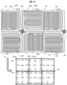
- FIG. 1 is a plan view showing a schematic arrangement of heaters, power supply parts, and return parts in a plurality of adjacent regions arranged on the upper surface of a sample stage in an embodiment.
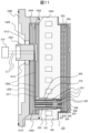
- FIG. 2 is a vertical sectional view showing a schematic outline of the structure of a lower part of a sample stage of the plasma processing apparatus according to the embodiment shown in FIG. 1;
- FIG. 12 is a perspective view showing a schematic outline of the overall configuration of the FPC provided under the sample stage shown in FIG.
- FIG. 13 is a perspective view that diagrammatically illustrates the outline of the configuration of the tip of the arm of the FPC shown in FIG.
- FIG. 14 is a plan view that illustrates an outline of the configuration of an FPC according to a modified example.
- Fig. 1 is a cross-sectional view showing a schematic outline of a configuration of a plasma processing apparatus according to an embodiment.
- Fig. 1 shows a plasma etching apparatus 100 that uses a microwave electric field as an electric field for forming plasma, generates an ECR (Electron Cyclotron Resonance) between the electric field and magnetic field of the microwave to form plasma, and uses the plasma to etch a substrate-like sample such as a semiconductor wafer.
- ECR Electro Cyclotron Resonance
- the plasma etching apparatus 100 has a vacuum vessel 101 with an internal processing chamber 104 where plasma is formed.
- the vacuum vessel 101 has a cylindrical shape and an open top, to which a dielectric window 103 (e.g., made of quartz) for introducing microwaves is disposed as a lid member, forming the processing chamber 104 with the inside and outside airtightly separated.
- a vacuum exhaust port 110 is disposed at the bottom of the vacuum vessel 101, and is connected to a vacuum exhaust device (not shown) disposed below and connected to the vacuum vessel 101.
- a shower plate 102 that constitutes the ceiling surface of the processing chamber 104 is provided below the bottom surface of the dielectric window 103 that constitutes the upper cover member of the vacuum vessel 101.
- the shower plate 102 has multiple gas introduction holes 102a located in the center, and etching process gas is introduced into the processing chamber 104 through these multiple gas introduction holes 102a.
- the shower plate 102 is a circular plate made of a dielectric material such as quartz.
- an electric field/magnetic field generating section 160 that generates an electric field and a magnetic field for generating plasma 116 is disposed at a location above the exterior of vacuum vessel 101.
- the electric field/magnetic field generating section 160 is provided in plasma etching apparatus 100 and includes the following configuration. That is, electric field/magnetic field generating section 160 is disposed above dielectric window 103, and includes a waveguide 105 through which an electric field is transmitted to supply a high-frequency electric field of a predetermined frequency for generating plasma 116 to processing chamber 104.
- the electric field transmitted inside the waveguide 105 is generated by oscillation in the electric field generating power supply 106.
- the frequency of the electric field is not particularly limited, but in this embodiment, microwaves of 2.45 GHz are used.
- magnetic field generating coils 107 that generate a magnetic field are arranged above the dielectric window 103 of the processing chamber 104, on the side wall of the vacuum vessel 101 that constitutes the cylindrical portion of the processing chamber 104, and on the outer periphery of the lower end of the waveguide 105, surrounding these.
- the electric field of the microwaves generated by the electric field generating power supply 106 propagates inside the waveguide 105, passes through the dielectric window 103 and the shower plate 102, and is supplied to the processing chamber 104 from above.
- the magnetic field generating coil 107 generates an ECR (Electron Cyclotron Resonance) by interacting with the magnetic field supplied into the processing chamber 104. Then, by exciting and dissociating the atoms or molecules of the processing gas introduced into the processing chamber 104 through the gas introduction holes 102a of the shower plate 102, a high-density plasma 116 is generated in the processing chamber 104.
- ECR Electro Cyclotron Resonance
- a wafer-mounting electrode (first electrode) 120 constituting a sample stage.
- the wafer-mounting electrode 120 has a mounting surface 120a on which a semiconductor wafer (hereinafter simply referred to as a wafer) 109, which is the sample (subject to be processed), is placed.
- the wafer-mounting electrode 120 is disposed so that its mounting surface 120a faces the shower plate 102 or the dielectric window 103.
- the wafer-mounting electrode 120 may also be described as the sample stage 120.
- the upper surface 120b of the wafer mounting electrode 120 is covered with a dielectric film 140 that constitutes the mounting surface 120a. Inside the dielectric film 140, multiple conductive films (electrostatic attraction electrodes) 111 for electrostatic attraction are arranged, which are connected to a DC power source 126 via a high-frequency filter 125 shown in FIG. 1.
- the conductive film 111 constitutes the mounting surface 120a of the sample stage 120, and is a film-like electrostatic adsorption electrode to which DC power for electrostatically adsorbing a semiconductor wafer is supplied.
- the conductive film 111 may be bipolar, in which one of the multiple film-like electrodes is given a different polarity from the other, or may be unipolar, in which the same polarity is given, but in this embodiment it is shown as unipolar.
- a high frequency power supply (first high frequency power supply) 124 and a matcher 129 are disposed closer to the electrostatic attraction electrode (conductive film 111) than the high frequency filter 125, and these high frequency power supply 124 and matcher 129 are connected to an electrode substrate 108 having a circular or cylindrical shape and made of a conductive material, which is disposed inside the wafer mounting electrode 120.
- the high frequency power supply 124 is connected to ground 112.
- the electrode substrate 108 may also be simply referred to as substrate 108.
- high frequency power (first high frequency power) of a predetermined frequency is supplied from the high frequency power supply 124 to the electrode substrate 108, and a bias potential is formed above the wafer 109, which is attracted and held on the upper surface of the wafer mounting electrode 120, during processing of the wafer 109.
- the sample stage has a wafer mounting electrode 120 to which high frequency power (first high frequency power) is supplied from the high frequency power supply 124 while the plasma 116 is being generated.
- multiple refrigerant flow paths 152 are arranged in a spiral or concentric manner around the central axis in the vertical direction of the electrode substrate 108 or the wafer-mounting electrode 120.
- a cooling refrigerant for cooling the electrode substrate 108 flows through these refrigerant flow paths 152.
- a recess 120d is disposed on the outer periphery of the upper part of the wafer mounting electrode 120, surrounding the upper part on the outer periphery of the mounting surface 120a.
- a susceptor ring 113 which is a ring-shaped member made of a dielectric material such as quartz or ceramics such as alumina, is placed on the ring-shaped upper surface of this recess 120d, which is formed at a lower height than the mounting surface 120a of the sample stage.
- the upper surface of the susceptor ring 113 When the upper surface of the susceptor ring 113 is placed on the recess 120d, the upper surface of the susceptor ring 113 has dimensions that make it higher than the mounting surface 120a of the wafer mounting electrode 120.
- the susceptor ring 113 is disposed on the outer periphery of the mounting surface 120a of the wafer mounting electrode (sample stage) 120, and covers the surface of the wafer mounting electrode 120.
- the susceptor ring 113 is configured to cover the upper surface and cylindrical side wall surface of the recess 120d, as well as the cylindrical side wall surface of the wafer mounting electrode 120 below the recess 120d.
- a plasma etching apparatus 100 in a vacuum transfer chamber that is depressurized to the same pressure as the processing chamber 104 inside a vacuum transfer vessel, which is another vacuum vessel connected to the side wall of the vacuum vessel 101, an unprocessed wafer 109 is placed on the arm tip of a wafer transfer robot arranged in the vacuum transfer chamber. Then, a gate, which is a passage connecting the vacuum transfer chamber and the processing chamber 104, is opened by the operation of a valve arranged in the vacuum transfer chamber, and the unprocessed wafer 109 is transferred into the processing chamber 104 while being placed on the arm tip of the robot.
- the wafer 109 that has been transferred to above the mounting surface 120a of the wafer mounting electrode 120 in the processing chamber 104 is transferred onto the lift pins by the vertical movement of the lift pins, and after being placed on the mounting surface, it is attracted to and held on the mounting surface 120a of the wafer mounting electrode 120 by the electrostatic force formed by the DC power applied from the DC power source 126.
- the etching gas has its flow rate or speed adjusted by a mass flow controller (not shown) and is introduced into the space between the dielectric window 103 and the quartz shower plate 102. After diffusing in this space, it is introduced into the processing chamber 104 through the gas inlet hole 102a of the shower plate 102. The gas and particles in the processing chamber 104 are then exhausted through the vacuum exhaust port 110 by the operation of the vacuum exhaust device. Depending on the balance between the amount of gas supplied from the gas inlet hole 102a of the shower plate 102 and the amount exhausted from the vacuum exhaust port 110, the inside of the processing chamber 104 is adjusted to a predetermined value within a range suitable for processing the wafer 109.
- a heat-conductive gas such as He (helium) is supplied from an opening (not shown) on the top surface of the dielectric film 140 to the gap between the wafer 109 and the top surface of the dielectric film 140, which is the mounting surface 120a of the wafer mounting electrode 120, thereby promoting heat transfer between the wafer 109 and the wafer mounting electrode 120.
- the temperature of the wafer mounting electrode 120 or the electrode substrate 108 is adjusted in advance before the wafer 109 is placed on it by circulating a coolant adjusted to a predetermined temperature range through the coolant flow passage 152 arranged in the electrode substrate 108 of the wafer mounting electrode 120.
- the temperature of the wafer 109 is adjusted to be close to these temperatures before processing, and even after processing begins, heat is transferred from the wafer 109 to adjust the temperature of the wafer 109.
- a microwave electric field and a magnetic field are supplied into the processing chamber 104, and plasma 116 is generated using the gas.
- radio frequency (RF) bias power is supplied from the radio frequency power supply 124 to the electrode substrate 108, a bias potential is formed above the upper surface of the wafer 109, and charged particles such as ions in the plasma 116 are attracted to the upper surface of the wafer 109 according to the potential difference with the potential of the plasma 116. Furthermore, the charged particles collide with a mask previously placed on the upper surface of the wafer 109 and the surface of the film layer to be processed of the film structure including the film layer to be processed, thereby performing an etching process.
- the processing gas introduced into the processing chamber 104 and particles of reaction products generated during the process are exhausted from the vacuum exhaust port 110.
- the plasma etching apparatus 100 supplies second high-frequency power from the high-frequency power source (second high-frequency power source) 127 to a conductor ring (second electrode) 131 located on the upper part of the outer periphery of the sample stage via a power supply connector 161 (described later) that is provided on the sample stage and has an elastic conductive member.
- the AC high voltage generated by the high frequency power source (second high frequency power source) 127 is introduced to a conductor ring (second electrode) 131 made of a conductive material arranged inside the susceptor ring 113 via a load matching unit 128 and a load impedance variable box 130.
- the impedance value for the high frequency power from the high frequency power source 127 through the electrode substrate 108 to the outer periphery of the wafer 109 is relatively low by combining the load impedance variable box 130 adjusted to a suitable impedance value with a relatively high impedance portion arranged on the upper part of the susceptor ring 113.
- the high frequency power supply 127 is connected to the ground 112.
- the frequency of the high frequency power supply 127 is preferably set to the same value as that of the high frequency power supply 124 or a constant multiple thereof.
- Figure 2 is a cross-sectional view showing a schematic view of a portion of the configuration of the sample stage of the plasma processing apparatus shown in Figure 1.
- Figure 3 is an enlarged cross-sectional view showing a schematic view of a portion of the configuration of the sample stage of the plasma processing apparatus shown in Figure 2.
- the disk- or cylindrical-shaped substrate 108 is arranged inside the sample stage 120 shown in FIG. 2 and is made of a metallic material such as titanium, aluminum, or a compound of these. It is electrically connected to the ground electrode S and is connected conductively to the wall surface of the vacuum vessel 100 shown in FIG. 1, and is fixed to the ground potential.
- the substrate 108 has a convex portion in the center on which the wafer 109 is placed, and a concave portion that is arranged in a ring shape on the outer periphery of the convex portion, surrounds the convex portion, and has a lowered top surface.
- a step that forms the outer circumferential sidewall of the protrusions is a step that forms the outer circumferential sidewall of the protrusions.
- a susceptor ring 113 made of a ceramic material is placed on the ring-shaped recess.
- a dielectric film 201 which is a film made of a dielectric material such as ceramics, is disposed on the flat upper surface of the convex portion of the substrate 108. Furthermore, on top of the film layer of this dielectric film 201, a plurality of first heater films (also called first heater layers) 202, which are film-like electrodes made of a conductive material and generate heat when DC power is supplied, are disposed covering a plurality of regions on the upper surface of the substrate 108. In other words, the dielectric film 201 is disposed on the upper surface of the substrate 108, and further, on top of this dielectric film 201, a heater film 202, which is a film-like heater, is formed.
- first heater films also called first heater layers
- the heater film 202 is further covered by an upper dielectric film 203, and the heater film 202 is surrounded by a dielectric member (dielectric film 203).
- the sample stage 120 is arranged on top of the dielectric film 201, and on top of the dielectric film 203 that covers the heater film 202, a plurality of second heater films (also called second heater layers) 204, which are film-like electrodes made of a conductive material of the same structure as above and generate heat when DC power is supplied, are arranged to cover multiple areas of the upper surface of the substrate 108.
- a dielectric film 205 is disposed so as to cover the heater film 204.
- a first heater film 202 surrounded by dielectric films 201 and 203 is disposed on the upper surface 120b of the substrate 108
- a second heater film 204 surrounded by dielectric films 203 and 205 is disposed on the upper surface of the first heater film 202 in the same manner as described above.
- Each of these heater films 202, 204 is connected to DC power sources 314, 315, whose operation is adjusted according to a command signal from the controller, via power supply cables (power supply lines, power supply paths) 316, 317, and is configured so that DC power can be supplied from the DC power sources 314, 315.
- the power supply cables 316, 317 are cables that electrically connect the heater films 202, 204 to the DC power sources 314, 315 that supply DC power to the heater films 202, 204.
- the power supply cables 316, 317 do not include a filter for high-frequency power.
- the inside of the dielectric film 201 arranged on the upper surface 120b of the sample stage 120 is configured to have a plurality of first heater films 202 (called multi-zone heaters) that can adjust the temperature of the upper surface of the dielectric film 201 by adjusting the amount of heat generated for each region (zone), and a plurality of second heater films 204 on top of them that can adjust the temperature of the upper surface.
- first heater films 202 called multi-zone heaters
- the sample stage 120 has a first heater film 202 surrounded by dielectric films 201 and 203 arranged on the upper surface 120b of the substrate 108, and a second heater film 204 surrounded by dielectric films 203 and 205 arranged on the upper surface of the first heater film 202 as described above. Furthermore, a shield film 206, which is a film-like conductive member arranged on the upper surface of the dielectric film 205 and surrounding the outer periphery of the upper and peripheral parts, is provided, and the heater films 202 and 204 are surrounded (covered) by the shield film 206.
- the structure in which the heater films 202 and 204 are surrounded by the shield film (conductor film) 206 is encapsulated by the dielectric material that constitutes part of the dielectric films 201, 203, and 205.
- the shield film 206 is electrically connected to the substrate 108, and as a result, the shield film 206 is fixed to the ground potential like the substrate 108, and as a result, the inflow of high frequency waves into the heater films 202 and 204 can be suppressed.
- a dielectric film 207 is disposed on the upper surface of the shielding film 206, and on top of this dielectric material member are disposed an electrode 111 for electrostatic attraction and an electrode film 208, which is an electrode to which high frequency power for forming a high frequency bias is supplied.
- the electrode film 208 is a film made of a conductive material, and is electrically connected to a high frequency bias power supply 313 that supplies high frequency power of a predetermined frequency.
- the electrode film 208 is also electrically connected to a DC power supply 312, and by applying a DC voltage, the wafer 109 placed on the mounting surface of the sample stage 120 can be attracted by static electricity.
- the DC power supply 312 corresponds to the DC power supply 126 in FIG. 1.
- a dielectric film (electrostatic adsorption member) 209 made of a ceramic material constituting the top surface of the sample stage 120 and the mounting surface on which the wafer 109 is placed is disposed, covering the top surface of the convex portion, the surrounding concave portion, and the step portion which is the side wall of the convex portion. That is, on the top surface of the sample stage 120, a dielectric film 209 is disposed on the shielding film 206, the dielectric film 209 including an electrode film (electrode) 208 which adsorbs the wafer 109 by electrostatic force disposed on the top of the shielding film 206.
- the dielectric film 140 in FIG. 1 can be regarded as the dielectric films 201, 203, 205, 207, and 209.
- the sample stage 120 has a plurality of through holes (301, 302, 303, 304, 305) that penetrate between the upper surface of the dielectric film 209 on the convex portion and the bottom surface of the substrate 108.
- These through holes include a plurality of lift pin through holes 302 that house lift pins (pins) 311 that move up and down inside to support the wafer 109 from below and move it above the upper surface of the sample stage 120, and a heat transfer gas supply hole 301 through which a heat transfer gas such as He flows to be supplied to the gap between the upper surface of the dielectric film 209 and the back surface of the wafer 109 placed thereon.
- the lift pins 311 arranged in the lift pin through holes 302 raise or lower the wafer 109 above the upper surface of the dielectric film 209.
- the multiple lift pin through holes 302 open on the top surface of the dielectric film 209 and penetrate the dielectric film 201, the dielectric film 203, the dielectric film 205 and the dielectric film 206.
- an electrostatic adsorption power supply hole 303 with a power supply cable and connector disposed therein for applying power to the electrode film 208
- a heater power supply hole 305 with a power supply path 317 and connector disposed therein for supplying power to the first grid-shaped heater film 202
- a heater power supply hole 304 with a power supply cable 316 and connector disposed therein for supplying power to the second ring-shaped heater film 204.
- the inner wall surface of the holes (301, 302, 303, 304, 305) that penetrate the inside of the base material 108 is provided with insulating bosses 306, 307, 308, 309, 310, which are cylindrical members made of a dielectric material or an insulating material. That is, the base material 108 of the sample stage 120 is provided with insulating bosses 306, 307, 308, 309, 310, which are cylindrical members made of an insulating material that form the inner wall surface of the base material 108 inside the base material 108 and are disposed inside each of the multiple through holes.
- the insulating bosses 306, 307, 308, 309, and 310 can suppress the occurrence of discharge in the space inside the hole that is exposed to the electric field caused by high frequency power during processing of the wafer 109.
- the insulating bosses 306, 307, 308, 309, and 310 can be made of ceramic materials such as alumina and yttria, or resin materials.
- the heater power supply hole 305 is provided with a plurality of power supply paths that supply power to the plurality of heater films 202, and an insulating connector 310 that is made of a dielectric material that surrounds the plurality of power supply paths and insulates each of the power supply paths.
- the insulating connector 310 is configured by connecting a plurality of cylindrical members in the vertical direction, and a conductive member such as a metal that constitutes the power supply path is arranged inside the plurality of cylindrical members.
- the lower insulating connector 322 which is at least the lowest member among the insulating members that constitute the insulating boss, is configured to be detachable (attachable and detachable) from the bottom (bottom surface) of the substrate 108.
- the lower insulating connector 322 has a cylindrical shape, and is configured so that the power supply path that supplies power to the first grid-shaped heater film 202 is connected or disconnected by attaching or detaching the lower insulating connector 322 to the bottom of the substrate 108.
- the lower insulating connector 322 can be rephrased as a power supply connector for supplying power to the heater film 202.
- the lower insulating connector 322 is inserted into the heater power supply hole 305 from below, and the bottom surface (lower end) of the upper insulating connector 321 made of an insulating material such as ceramics arranged at the top inside the heater power supply hole 305 faces or comes into contact with the upper surface (upper end) of the lower insulating connector 322.
- the lower part of each of the multiple power supply pins 320 that penetrate the center of the upper insulating connector 321 is inserted into the multiple insertion holes 318 arranged in the center of the lower connector 322.
- the insertion hole 318 can be called a through hole.
- the upper insulating connector 321 is composed of three upper and lower members (an upper insulating sleeve, a screw-in sleeve, and a lower insulating sleeve).
- the uppermost upper insulating sleeve constituting the upper insulating connector 321 has the power supply pin 320 inserted in the center, and while holding the power supply pin 320, is inserted into the upper end of the heater power supply hole 305 of the substrate 108 and fixed in position with adhesive. In this state, the position of the power supply pin 320 is also fixed.
- a ceramic adhesive can be used as this adhesive, and the upper insulating sleeve and the heater power supply hole 305 are vacuum sealed with the ceramic adhesive.
- the power supply pin 320 is composed of a rod-shaped conductive member having a cylindrical shape. The upper end of the power supply pin 320 is configured to be connected to the bottom surface of the first heater film 202 formed on the dielectric film 203.
- the upper insulating sleeve (with the multiple power supply pins 320 held in the center of the upper insulating sleeve) is inserted into the heater power supply hole 305, and with the upper insulating sleeve joined to the top of the heater power supply hole 305, a cylindrical screw-in sleeve made of an insulating material is inserted into the heater power supply hole 305. The screw-in sleeve is then screwed in so that the threads formed in advance on the cylindrical side wall surface engage with the threads formed on the inner peripheral side wall surface of the heater power supply hole 305.
- the upper insulating sleeve is supported from below by the screw-in sleeve as the upper end of the screw-in sleeve is screwed in until it comes into contact with the bottom surface (lower end) of the upper insulating sleeve.
- the cylindrical lower insulating sleeve is inserted into the heater power supply hole 305 until the upper end of the lower insulating sleeve comes into contact with the bottom surface (lower end) of the screw-in sleeve. Then, an insulating adhesive is sandwiched between the cylindrical side surface of the lower insulating sleeve and the inner side wall surface of the heater power supply hole 305 to bond them.
- a silicone-based adhesive can be used as the insulating adhesive.
- the lower insulating connector 322 is inserted into the heater power supply hole 305 from below.
- the power supply pin 320 is inserted into the inside of each through hole 318 arranged in an axially symmetrical position around the vertical axis in the central region of the circular upper surface of the lower insulating connector 322. Then, the power supply pin 320 comes into contact with a conductive connector terminal arranged inside each through hole 318.
- Each of the connector terminals inside the multiple through holes 318 of the lower insulating connector 322 is connected to a DC power source 315 via each power supply path 317.
- the substrate 108 connected to the ground electrode S is insulated from the power supply path 317 and the power supply pin 320 by the upper insulating connector 321, adhesive (silicone-based adhesive in this example), and lower insulating connector 322.
- the processing chamber 104 and the inside of the heater power supply hole 305 which is kept at atmospheric pressure or a pressure close to atmospheric pressure, are hermetically separated by an adhesive (ceramic-based adhesive in this example) that joins the upper insulating connector 321 and substrate 108.
- the devices that adjust the operation of the plasma etching apparatus 100 including the electric field generating power supply 106, the magnetic field generating coil 107, the high frequency power supply 124, the high frequency filter 125, the DC power supply 126, the high frequency power supply 127, the matching box 128, 129, the load impedance variable box 130, and other electric field/magnetic field adjustment systems, as well as the DC power supplies 314, 315 that supply power to the first heater film 202 and the second heater film 204 inside the dielectric film 201, and the devices that configure the pressure adjustment system, such as the vacuum exhaust device and the mass flow controller that adjusts the gas supply amount described below, each have a detector that detects the operating state such as output, flow rate, pressure, etc., or a plurality of temperature sensors located inside the substrate 108 of the wafer mounting electrode 120, and are connected to the control unit 170 so as to be able to communicate via wire or wirelessly.
- the calculator of the control unit 170 When signals indicating the operating status of each of these devices output from the detectors provided in each of these devices are transmitted to the control unit 170, the calculator of the control unit 170 reads out software stored in the internal storage device of the control unit 170 and detects the amount of that status from the signals received from the detectors based on the algorithm, and calculates and transmits a command signal to adjust this to an appropriate value.
- the devices included in the electric field/magnetic field adjustment system, DC power supplies 314, 315, or pressure adjustment system that receive the command signal adjust their operation in response to the command signal.
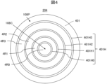
- FIG. 4 is a diagram showing an example of the arrangement of the second heater film inside the sample stage.
- the heater arrangement 401 shown in FIG. 4 is an example of the arrangement of multiple ring-shaped second heater films 204 inside the sample stage 120.
- Each heater film 204 has a heater wire inside, and the purpose of the heater film 204 is to perform temperature control according to the reaction product distribution and plasma density distribution during plasma processing of the wafer 109.
- the second heater layer 204 includes a plurality of film-shaped heater parts 401H (401H0, 401H1, 401H2, 401H3).
- the plurality of film-shaped heater parts 401H (401H0, 401H1, 401H2, 401H3) are disposed inside the dielectric film (dielectric film 203, 205) above the first heater layer 202, on a plurality of radii in the radial direction from the center (108C) of the upper surface of the substrate 108 of the sample stage 120 toward the outer periphery (108P), in each of three or more radial regions (4R0, 4R1, 4R2, 4R3) including circular regions arranged concentrically around the center and ring-shaped regions surrounding the outer periphery of the circular regions.
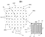
- FIG. 5 is a diagram showing an example of the arrangement of the first heater film provided on the sample stage of the plasma processing apparatus according to this embodiment.
- the film-like first heater film 202 of this embodiment is a metal film-like heater arranged inside the dielectric film 140 that covers the circular upper surface of the substrate 108 in multiple layers, and is arranged in multiple regions 501 corresponding to each of the circuit patterns of multiple semiconductor devices formed in advance on the upper surface of the wafer 109 placed on the upper surface of the dielectric film 209 when viewed from above.
- the region 501 is not a perfect rectangular shape but has a partially arc-shaped ARC.
- the first heater film 202 is provided to adjust the temperature of each circuit pattern (also called a die or chip area) of the semiconductor device formed on the wafer 109 during plasma processing.
- the first heater film 202 has, in the rectangular region 501, a rectangular outer frame wiring portion 501CL and an internal wiring portion 801 formed inside the outer frame wiring portion 501CL.
- the internal wiring portion 801 is connected, for example, between a pair of opposing corners (cna, cnc) at the four corners (first corner cna, second corner cnb, third corner cnc, fourth corner cnd) of the outer frame wiring portion 501CL.
- the pair of corners (cna, cnc) are diagonal corners.
- the internal wiring section 801 is a film-like heater wire, and is configured, for example, with a meandering heater wiring (also called a meander wiring) between a pair of opposing corners (cna, cnc) of the outer frame wiring section 501CL so as to heat the entire internal region of the outer frame wiring section 501CL.
- the outer frame wiring section 501CL has a first side SL1 provided between the first corner cna and the second corner cnb, a second side SL2 provided between the second corner cnb and the third corner cnc, a third side SL3 provided between the third corner cnc and the fourth corner cnd, and a fourth side SL4 provided between the fourth corner cnd and the first corner cna.
- the first side SL1 and the third side SL3 are arranged opposite each other, the second side SL2 is arranged between the first side SL1 and the third side SL3, and the fourth side SL4 is arranged opposite the second side
- the outer frame wiring portion 501CL of the first heater film 202 is rectangular in shape inside each of a plurality of rectangular regions 501 divided into a grid shape by a plurality of first line segments (RL) that are parallel and extend in the front-rear direction at equal intervals on the upper surface of the dielectric film 201 in accordance with the shape of the die of the semiconductor device, and a plurality of second line segments (CL) that are perpendicular to the plurality of first line segments (RL) and extend in the front-rear direction at equal intervals.
- the outer frame wiring portion 501CL is rectangular in shape to match the outer shape of each region 501.
- the region 501 is not completely rectangular, but has a partly arc-shaped ARC, so that the outer frame wiring portion 501CL is shaped to match the outer shape of the region 501 with the arc-shaped ARC (see FIG. 6 for this).
- the number of regions 501 of the first heater film 202 is greater than the number of regions (4R0, 4R1, 4R2, 4R3 in this example) of the heater arrangement 401 of the multiple ring-shaped second heater film 204 shown in FIG. 4. While the number of regions (4R0, 4R1, 4R2, 4R3 in this example) of the heater arrangement 401 is, for example, 3 to 40, the number of regions 501 can be, for example, 10 to 200.
- a thin metal film constituting the first heater layer 202 is folded back horizontally multiple times along the sides of the rectangular outer shape to form a rectangular film-like heater wire (801).
- the temperature of the wafer 109 can be precisely adjusted for each location on the top surface of the wafer 109 corresponding to each die of the semiconductor device of the wafer 109.
- the film thickness of the multiple film heaters formed by the second heater layer 204 is configured to be larger (thicker) than the film thickness of the multiple film heaters 801 formed by the first heater layer 202.
- a plurality of temperature sensors TS are disposed inside the substrate 108 below the first heater film 202.
- the plurality of temperature sensors TS are electrically connected to the control unit 170, for example, by metal wiring, and the temperature values measured and detected by the plurality of temperature sensors TS are configured to be transmitted to the control unit 170 via the metal wiring.
- the control unit 170 receives the output from the temperature sensor TS and detects the temperature of the top surface of the substrate 108 or the surface of the dielectric film 201 corresponding to each zone (501) according to the algorithm of the software stored in the internal storage device. The control unit 170 then adjusts the amount of DC power supplied to the heater wire (801) of each zone (501) according to the algorithm of the software that was also read out based on the detected temperature, thereby adjusting the heat generation amount of the heater wire (801) of each zone (501) or the heat generation amount on the substrate 108.
- control unit 170 is configured to perform feedback control based on the detected temperatures corresponding to the outputs from the multiple temperature sensors TS so that the heat generation amount of the film-like heater wire (801) constituting the first heater layer (202) of each zone (region 501) or the heat generation amount on the substrate 108 becomes the desired heat generation amount or the desired heat generation amount.
- the heater wire (801) that is feedback controlled is the first heater film 202.
- the second heater film 204 maintains a predetermined amount of power supply to the heater in each of the ring-shaped zones (4R0, 4R1, 4R2, 4R3) of connected circular or arc-shaped regions shown in FIG. 4 for each wafer 109 or for each type of film structure on the top surface of the wafer 109, or for each batch (lot) of a predetermined number of wafers 109.
- the amount of heat generated by the second heater film 204 is fixed, and the temperature of the first heater film 202 (heater wire 801) is adjusted according to the temperature obtained by output from the temperature sensor TS.
- control unit 170 adjusts the output of the film heater 801 located within one of the rectangular regions (region 501, CH1-CH4 in Figures 7 and 8) of the first heater layer 202, while maintaining the output of the heater of the second heater layer 204 located above one of the rectangular regions (region 501, CH1-CH4 in Figures 7 and 8) corresponding to the die of the semiconductor device, in response to the output from the multiple temperature sensors TS.
- FIG. 6 is a top view that shows a schematic arrangement of the first heater films 202 arranged in multiple grid-shaped areas on the sample stage according to this embodiment shown in FIG. 5, and the power supply section (601) and current return section (701) to each first heater film 202.
- FIG. 6 shows an example of the arrangement of the power supply section (601) and current return section (701) together with the arrangement of the grid heater (first heater film 202).
- the four grid-shaped regions 501 are formed by connecting two regions 501 in the front-to-back and left-to-right directions to form a rectangular region as a whole, and the current return section (also called return path) 701 is located at the corner of each of the four grid-shaped regions 501, which is the center of the entire region, and the power supply section 601 of each region 501 is located at the corner diagonally opposite the corner where the current return section 701 is located.
- a current return section (701) is arranged in the center, and power supply sections (601) are arranged at the four corners.
- the four film heaters 801 arranged in each of the four regions (CH1-CH4) are treated as one group, and four power supply paths (power supply sections 601) that are electrically connected to one location (A, B, C, D) of each of the film heaters 801 in this group and supply power from the DC power source 315, and one return path (701) that is electrically connected to another location (G) of each of the film heaters 801 and returns power to the DC power source 315 are provided.
- one return path (701) is electrically connected to each end of multiple film heaters 801 arranged in multiple adjacent regions (CH1-CH4), and is configured so that the supplied power returns to the DC power source 315 via each end of the heaters 801 and the substrate 108.
- the connector parts of the power supply unit 601 and the connector parts of the current return unit 701 are arranged alternately at the boundaries (corners) of two areas 501 on the boundaries of the grid in the front-back and left-right directions that divide the areas 501 arranged in a lattice pattern.
- Each of the boundaries that divide the grid-shaped regions 501 in the front-back and left-right directions is disposed through the center of the top surface of the circular substrate 108 or dielectric film 203.
- four rectangular regions 501, two of which are adjacent to each other cannot be configured as a single group, so three grid-shaped regions 501 are disposed as a set.
- These regions 501 or first heater films 202 at the outer periphery may be composed of two or three.
- the connector portion of the supply portion 601 and the connector portion of the current return portion 701 are arranged in a set (SET2) of three grids.
- the connector part of the current return part (701) is made of a conductive material and is connected to the substrate 108, which is grounded and electrically set to ground potential, by tungsten via wiring. With this configuration, the current supplied to the first heater film 202 flows through the current return part 701 to the substrate 108, which is set to a constant voltage (ground potential).
- the labor and cost of manufacturing the sample stage 120 or plasma processing device can be reduced.
- the number of holes required for the return current to be processed in the substrate 108 can be reduced.
- processing vias on the substrate 108 and forming tungsten via wiring between the first heater layer 202 and the substrate 108 it becomes possible to collect the return current of the heater wire 801 in the substrate 108.
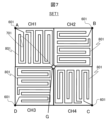
- Figure 7 is a top view that shows a schematic outline of the configuration of the first heater film 202 of the set of four regions (SET1) on the sample stage 120 shown in Figure 6. It shows an enlarged view of the heater wire (801) of the first heater film 202 in each region 501.
- FIG. 8 is a diagram showing a schematic of the current flowing through the first heater film 202 between the power supply section 601 and the current return section 701 in the set of four regions (SET1) shown in FIG. 7.
- FIG. 8 shows an equivalent circuit diagram in which the four heater wires 801 shown in FIG. 7 are rewritten as four resistance elements (R1, R2, R3, R4).
- FIG. 8 also shows the relative magnitude of the potential of the power supply section 601 with respect to the potential of the current return section 701 (ground potential in this embodiment) as positive and negative polarity.
- the positive and negative signs (+, -) and arrangement in FIG. 8 show the potential of the power supply section (601) higher than the potential of the return section 701 with "+" and lower with "-".
- one set (SET1) is composed of four grids, and the four grids are composed of four regions (CH1, CH2, CH3, CH4) corresponding to the four dies of the semiconductor device.
- One set (SET1) is rectangular in plan view and has four corners (A, B, C, D) and a center point (G). The four corners (A, B, C, D) are arranged in the order of the first corner A, the second corner B, the third corner C, and the fourth corner D in a clockwise direction in plan view.
- first corner A and the third corner C correspond to a pair of opposing corners.
- the second corner B and the fourth corner D correspond to another pair of opposing corners.
- the first region CH1 is disposed in the rectangular portion between the first corner A and the center point (G).
- the power supply section 601 is disposed in the first corner A, and the current return section 701 is disposed in the center point (G).
- a heater wire (801) is connected between the power supply section 601 in the first corner A and the current return section 701 in the center point (G).
- the second region CH2 is disposed in the rectangular portion between the second corner B and the center point (G).
- the power supply section 601 is disposed in the second corner B.
- a heater wire (801) is connected between the power supply section 601 in the second corner B and the current return section 701 in the center point (G).
- the third region CH3 is located in the rectangular portion between the third corner C and the center point (G).
- the power supply unit 601 is located in the third corner C.
- a heater wire (801) is connected between the power supply unit 601 in the third corner C and the current return unit 701 in the center point (G).
- the fourth region CH4 is located in the rectangular portion between the fourth corner A and the center point (G).
- the power supply unit 601 is located in the fourth corner D.
- a heater wire (801) is connected between the power supply unit 601 in the fourth corner D and the current return unit 701 in the center point (G).
- the first region CH1 and the second region CH2 are arranged rotationally symmetrically with respect to the center point (G).
- the first region CH1 and the third region CH3, and the first region CH1 and the fourth region CH4 are also arranged rotationally symmetrically with respect to the center point (G).
- the four first to fourth regions (CH1-CH4) are arranged with one side of each rectangle facing the adjacent region.
- the current return section 701 which is a return path
- the current return section 701 is disposed at the location (G) where the four corners of each of the four mutually adjacent rectangular regions (CH1-CH4) are adjacent to each other.
- the power supply section (601) which is a power supply path, is connected to the corners (A, B, C, D) diagonally opposite the corner to which the return path (701) is connected.
- FIG. 9 is a schematic diagram showing the relationship between the four corners (first corner cna, second corner cnb, third corner cnc, fourth corner cnd) and four sides (first side SL1, second side SL2, third side SL3, fourth side SL4) of the rectangular region 501 described in FIG. 5 and the four regions (first region CH1, second region CH2, third region CH3, fourth region CH4) in FIG. 7.
- the second region CH2 is positioned by rotating the first region CH1 90 degrees to the right with respect to the center point (G) or the third corner cnc, so that the second side SL2 of the first region CH1 overlaps with the third side SL3 of the second region CH1.
- the third region CH3 is positioned by rotating the second region CH2 90 degrees to the right with respect to the center point (G), so that the second side SL2 of the second region CH1 overlaps with the third side SL3 of the third region CH3.
- the fourth region CH4 is positioned by rotating the third region CH3 90 degrees to the right with respect to the center point (G), so that the second side SL2 of the third region CH1 overlaps with the third side SL3 of the fourth region CH3. And, the second side SL2 of the fourth region CH1 overlaps with the third side SL3 of the first region CH3.
- the four first to fourth regions are arranged with one side of the rectangle (second side SL2 and third side SL3) facing the adjacent region (first region CH1 and second region CH2, second region CH2 and third region CH3, third region CH3 and fourth region CH4, fourth region CH4 and first region CH1).
- the center point (G) is adjacent to the third corners cnc of the four regions (first region CH1, second region CH2, third region CH3, fourth region CH4).
- the potential of at least one of the connector parts of the power supply part 601 located at the diagonal corners (B, D) of the corners (A, B, C, D) of each of the four areas 501 in which the current return part 701 is arranged is set to a negative potential (-) with respect to the connector part of the current return part 701 set to a ground potential (0V).
- the polarity of the potential of the connector part set to a positive potential (+) value in two power supply parts 601 is set to a negative potential (-) value that is the inverse of the potential in the other two power supply parts 601.
- the potential of at least one point (A, B, C, or D) where each film heater (801) is connected to each of the four power supply parts (601) that are the power supply paths is made lower (negative potential (-)) than the potential (0V: ground potential) of the point (G) where each film heater (801) is connected to one return path (701).
- the number (2) of power supply parts 601 with a high potential (+) relative to the current return part 701 is set to two, the same as the number (2) of power supply parts 601 with a low potential (0-).
- the set (SET1) of four grid-like regions 501 is arranged with rotational symmetry with respect to the center (G).
- the number of power supply parts 601 (the number of positive potentials (+)) is equal to the number of power supply parts 601 that are not inverted (the number of negative potentials (-))
- the magnitudes of the currents (I1, I2, I3, I4) flowing through the heater wires 801 located at positions that are line-symmetric or point-symmetric with respect to the center point G (current return part 701) are equal, and it is guaranteed that the apparent current flowing through the substrate 108 is half that in the case where the polarity is not inverted.
- the temperature of the heater wires 801 becomes almost the same under flat temperature conditions or temperature conditions where the temperature near the center of the electrode is high. In this case, it is expected that the return current of the current return portion 701 can be suppressed to about one-third compared to the case where the polarity is not reversed.
- the current flowing through the substrate 108 increases as the number of heater wires 801 increases. Joule heat is generated in the substrate 108 in proportion to the square of the magnitude of the current flowing through the substrate 108, affecting the temperature control of the wafer 109. Alternatively, a large amount of current flowing through the substrate 108 may pose a risk of electric shock.
- Figure 10 is a plan view that shows the arrangement of heaters, power supply units, and return units in multiple adjacent regions arranged on the upper surface of the sample stage in this embodiment.
- Figure 10 shows the reference symbols of the four first to fourth regions (CH1-CH4) shown in Figures 7, 8, and 9, and the corresponding relationship with the first to fourth regions (CH1-CH4) shown in Figure 9.
- the explanation of Figure 9 can be referred to for the sides, corners, and layout arrangement of the first to fourth regions (CH1-CH4) shown in Figure 10, so duplicate explanations will be omitted.
- the point where the corners A, B, C, and D of the first to fourth regions (CH1-CH4) are butted together is the power supply unit 601.
- a heater power supply hole 305 having an opening on the bottom surface of the substrate 108 is provided, and a lower insulating connector 322 is inserted and attached to this heater power supply hole 305, so that power is supplied to multiple film-like heater wires 801 arranged in the first to fourth regions (CH1-CH4) via the lower insulating connector 322.
- the first heater film 202 (heater wire 801) of this embodiment is disposed on the dielectric film 201 and inside the dielectric film 203 over almost the entire rectangular area, with the heater wire 801 of a predetermined width arranged back and forth along the sides of the rectangle.
- the four corners corresponding to the corners A, B, C, and D shown in FIG. 7, FIG. 8, and FIG. 9
- one end of each of the heater wires 801 in the four areas is disposed, and below the points is disposed a power supply unit 601 in which a power supply pin 320 (not shown) (see FIG. 3) is connected to one end of each of the heater wires 801. Power from the DC power source 315 is supplied to each heater wire 801 from the power supply unit 601 through one end.
- the four power supply pins 320 are fixed and arranged symmetrically around the vertical central axis of the cylindrical upper insulating connector 321, which is arranged at the top of the heater power supply hole 305, and the lower end of each power supply pin 320 protruding below the upper insulating connector 321 is inserted into four through holes 318 arranged symmetrically around the central axis of the lower insulating connector 322 and connected to the terminals, with the cylindrical lower insulating connector 322 inserted into the heater power supply hole 305 from below.
- Each power supply pin 320 is electrically connected to the DC power source 315 through the terminal in the through hole 318.
- each power supply pin 320 is connected to one end of each heater wire 801 in four different regions arranged with their corners butted together, and DC power is supplied.
- Each of these four regions (first region to fourth region: CH1-CH4) has a different set of heaters to which the internal heater wire 801 belongs, and one power supply unit 601 is configured to be able to supply power to four different sets of heaters when the power supply pin 320 is inserted into the through hole 318.
- Figure 11 is a vertical cross-sectional view that shows a schematic outline of the structure of the lower part of the sample stage of the plasma processing apparatus according to the embodiment shown in Figure 1.
- a space is arranged in which a power supply path to the heater films 202, 204 is arranged.
- This space is hermetically sealed and partitioned from the processing chamber 104, is connected to the space outside the plasma processing apparatus 100, and is maintained at atmospheric pressure or approximately atmospheric pressure.
- the lower end of the lower insulating connector 322 is connected to the tip of a flexible printed circuit (FPC) 1002 having multiple power supply wiring 1008 for the heater film 202 inside.
- the FPC 1002 connected to the circular bottom surface of the lower end of each cylindrical lower insulating connector 322 has multiple arms 1200 that have a predetermined width and extend in the horizontal direction (up and down in the figure).
- Each of the multiple arms 1200 is mainly provided between the lower end of the corresponding lower insulating connector 322 and the corresponding collective connector 1007, and is arranged to extend along the bottom surface of the base material 108.
- the flexible printed circuit board 1002 can be said to be a wiring member composed of a plate-shaped member made of resin, and has multiple power supply wiring 1008 inside to which power for the heater film 202 is supplied from the DC power source 315. Therefore, the multiple film-like heater wires 801 arranged in the multiple regions, the first region to the fourth region CH1-CH4, are electrically connected to each of the multiple power supply wirings 1008 of the flexible printed wiring board 1002 via the lower insulating connector 322, which is a power supply connector.
- the bottom surface of the substrate 108 of the sample stage 120 is provided with a plurality of through holes (e.g., thermally conductive gas supply hole 301, lift pin through hole 302, electrostatic adsorption power supply hole 303, heater power supply hole 304 of the second heater film 204, through holes through which the detection wiring of the plurality of temperature sensors TS passes, etc.). Therefore, the power supply wiring to the lower insulating connector 322 provided in the plurality of power supply parts 601 needs to be provided while bypassing the installation area of the plurality of through holes provided in the bottom surface of the substrate 108.
- the plurality of arms 1200 of the flexible printed wiring board 1002 have the effect of easily making it possible to bypass the installation area of the plurality of through holes.
- the width of the arm 1200 is, for example, slightly smaller than the diameter of one of the lower insulating connectors 322.
- the top surface of the tip of a corresponding one of the arm 1200 is joined to the bottom surface of the corresponding lower insulating connector 322.
- the power supply wiring 1008 arranged inside the FPC 1002 corresponding to the arm 1200 is a set of four power supply wirings, and each tip of one end of the four power supply wirings is electrically connected to each terminal that engages and contacts with the power supply pins 320 arranged inside each of the four through holes 318.
- the other ends of the multiple power supply wirings 1008 arranged inside each of the multiple arms 1200 are connected to each of the multiple power supply lines arranged inside the collective connector 1007 arranged in the center in contact with the bottom surface of the FPC 1002.
- multiple power supply lines extending in the vertical direction are grouped together as a group, with their upper ends connected to the power supply wirings 1008 arranged inside the multiple arms 1200.
- the lower ends of the multiple power supply lines form a connector section at the bottom of the collective connector 1007 that is connected to the power supply path 317 that electrically connects these power supply lines to the DC power source 315, and another connector that forms the tip of the power supply path 317 is connected to this connector section.
- the heater wires 801 arranged over almost the entire rectangular area are basically grouped into four in the central part of the upper surface of the sample stage 120, and two or three in the peripheral part, which have a common return section 701 (see FIG. 6).
- the power supply section 601 is arranged where the corners (C, D, B, A) of the four areas 802A to 802D of each rectangular first heater film 202 are butted together, and the upper insulating connector 321, lower insulating connector 322, and four power supply pins 320 are arranged below the power supply section 601.
- the upper insulating connector 321 is connected to the power supply sections 601 of the multiple first heater films 202, and the lower insulating connector 322 connected to the upper insulating connector 321 is connected above the tip of the arm section 1200 of the FPC 1002.
- the number of arms 1200 of the FPC 1002 is the same as the number of lower insulating connectors 322. Also, the number of arms 1200 of the FPC 1002 is the same as the number of upper insulating connectors 321.
- the regions 802A (CH4), 802B (CH3), 802C (CH2), and 802D (CH1) shown in FIG. 10 and the heater wires 801A, 801B, 801C, and 801D arranged therein each belong to different heater groups.
- the power supply path insulated from the substrate 108 by the upper insulating connector 321 connected to the power supply unit 601 and the connected lower insulating connector 322 is connected to a different heater group.
- the arm portion 1200 of the FPC 1002 is disposed below the bottom surface of the substrate 108 and extends along its surface.
- an assembly connector 1007 is disposed, which is in contact with the underside of the FPC 1002 and has a predetermined height.
- the assembly connector 1007 is connected to another connector (not shown) that constitutes the power supply path 317, thereby electrically connecting the power supply unit 601 and the DC power source 315 with the lower insulating connector 322 connected to the upper insulating connector 321.
- Insulating plates 1003 and 1004 are arranged between the FPC 1002 and the bottom surface of the upper substrate 108 and between the FPC 1002 and the universal plate 1006 made of a conductor such as metal arranged below.
- the insulating plates 1003 and 1004 cover the FPC 1002 and prevent electrical contact between the substrate 108 and the universal plate 1006 and the FPC 1002 and the lower insulating connector 322.
- the upper insulating plate 1003 has through holes 1011 arranged at positions corresponding to the multiple heater power supply holes 305.
- the lower insulating connector 322 joined to the tip of the arm 1200 of the FPC 1002 is inserted into the heater power supply hole 305 through the through hole 1011 from the lower side of the bottom surface of the insulating plate 1003 attached to the bottom surface of the substrate 108.
- Each of the insulating plates 1003 and 1004 is a circular plate-like member, and the insulating plates 1003 and 1004 are configured to be connectable in the vertical direction. At least one of the opposing surfaces of the insulating plates 1003 and 1004 has a recess so that a gap 1005 is formed in the region of the connection of the insulating plates 1003 and 1004 when the insulating plates 1003 and 1004 are connected.
- the FPC 1002 and the arm portion 1200 are stored in the gap 1005 formed between the insulating plates 1003 and 1004.
- the height of the lower insulating connector 322 is configured to protrude from the bottom surface of the substrate 108 when connected to the upper insulating connector 321, and is at least greater than the vertical length of the through hole 1011 of the upper insulating plate 1003, i.e., the thickness of the FPC 1002.
- a through hole 1012 is arranged in the center of the lower insulating plate 1004.
- an assembly connector 1007 connected to the underside of the center of the FPC 1002 sandwiched between the insulating plates 1003 and 1004 is inserted into the through hole 1012.
- the lower end of the assembly connector 1007 may protrude below the universal plate 1006 through the through hole 1012.
- the insulating plate 1004 sandwiches the FPC 1002 between the insulating plate 1003, covers the FPC 1002 from below, and is attached to the insulating plate 1003 or the substrate 108. This holds the FPC 1002 inside a gap 1005 that has a height slightly greater than the vertical thickness of the FPC 1002. This suppresses vertical movement of the FPC 1002, and in particular, vertical movement of the lower insulating connector 322 joined to the tip of the arm 1200. This reduces unintended breaks in engagement or connection between the lower insulating connector 322 and the power supply pin 320.
- a universal plate 1006 is provided.
- the universal plate 1006 is disposed below the substrate 108 and the insulating plates 1003 and 1004, and is configured to have a disk shape in which the peripheral portion of the upper surface of the universal plate 1006 is connected to the peripheral portion of the bottom surface of the substrate 108.
- the upper end of the outer peripheral portion of the upper part of the universal plate 1006 is attached to the outer peripheral portion of the bottom surface of the substrate 108 with a sealing member such as an O-ring sandwiched therebetween, and the space inside the processing chamber 104 is airtightly sealed.
- a cylindrical recessed portion that forms a gap 1010 is provided in the center of the upper surface of the universal plate 1006.
- the cylindrical recessed portion that forms the gap 1010 is configured to accommodate the insulating plate 1003 attached to the bottom surface of the substrate 108 and the insulating plate 1004 in a state in which the FPC 1002 is held within the gap 1005.
- the outer peripheral edge of the bottom surface of the universal plate 1006 is attached by sandwiching a sealing member such as an O-ring between it and a circular member of the plasma etching apparatus 100 disposed below the sample stage 120, and the space inside the processing chamber 104 is airtightly sealed.
- a recess 1009 recessed upward is disposed in the center of the bottom surface of the universal plate 1006, and a power supply path to the heater film 204, a connector of the power supply path to the electrode film 208, and a temperature sensor that detects the local temperature of the substrate 108 are attached to the bottom surface (recess 1009) of the universal plate 1006.
- the power supply path to the heater film 204, the connector of the power supply path to the electrode film 208, and the temperature sensor that detects the local temperature of the substrate 108 are inserted into the substrate 108 through the universal plate 1006 and the insulating plates 1003 and 1004.
- the space below the sample stage 120, which the bottom surface of the universal plate 1006 faces, is a space at atmospheric pressure or a pressure close to it, and the inside of the gap 1005 and heater power supply hole 305 that communicate with this space are also at the same pressure.
- a through hole 1013 is disposed in the center of the upper part of the universal plate 1006, and with the universal plate 1006 connected to the base material 108, an assembly connector 1007 connected to the underside of the center of the FPC 1002 is inserted into the inside of the through hole 1013.
- the lower end of the assembly connector 1007 may protrude downward from the lower end of the through hole 1013.
- Another connector constituting the power supply path 317 is connected to the assembly connector 1007 within the recess 1009 of the universal plate 1006.
- FIG. 12 is a perspective view that shows a schematic outline of the overall configuration of the FPC according to the embodiment shown in FIG. 11.
- FIG. 12 shows one configuration example of the FPC 1002, but the configuration of the FPC 1002 is not limited to that shown in FIG. 12.
- Multiple sets, for example, two, three, or four sets, of the FPC 1002 (including the multiple arms 1200) and the assembly connector 1007 may be provided for one base material 108 of the sample stage 120.
- the multiple through holes vertical hole structures provided in the base material 108, such as the heat transfer gas supply hole 301, the lift pin through hole 302, the electrostatic adsorption power supply hole 303, the heater power supply hole 304 of the second heater film 204, the through holes through which the detection wiring of the multiple temperature sensors TS passes, etc.
- the FPC 1002 including the multiple arms 1200
- the collective connector 1007 for one base material 108.
- the FPC 1002 has multiple arms 1200 (1201-1207) (seven arms are shown in FIG. 12 as an example).
- the multiple arms 1201-1207 extend from the center of the bottom surface of the FPC 1002 toward its outer periphery, and each has a predetermined width.
- a cylindrical lower insulating connector 322 is connected to the upper surface of the tip of each of the arms 1201-1207.
- seven lower insulating connectors 322 of the same size and shape are connected to the tip of each arm 1201-1207.
- the heater power supply hole 305 and through hole 1011 into which the lower insulating connectors 322 are inserted have the same diameter and depth, and the upper insulating connector 321 that contacts the lower insulating connector 322 also has the same size and shape.
- a collective connector 1007 is connected to the underside of the center of the FPC 1002, and the collective connector 1007 protrudes downward (upward in the figure) at a predetermined height from the underside of the FPC 1002.
- a recess 1009 is formed on the inside of the lower part of the collective connector 1007, and the collective connector 1007 may protrude into the recess 1009.
- the upper ends of the multiple terminals TT or the wires connected to the terminals TT arranged in parallel and spaced apart in the left-right and front-back directions inside the collective connector 1007 are connected to the ends of the multiple power supply wires 1008 built into the FPC 1002 inside the FPC 1002 above the upper end of the collective connector 1007.
- Each of the multiple power supply wires 1008 is arranged inside each of the arms 1201-1207, and the other ends of the power supply wires 1008 are electrically connected to the terminals housed inside the multiple through holes 318 of the lower insulating connector 322 connected to the ends of the arms 1201-1207.
- the FPC 1002 is sandwiched between an upper insulating plate 1003 connected to the bottom surface of the substrate 108, and the lower insulating connectors 322 are inserted into the interior through through holes 1011 formed at locations that align with the vertical axis to correspond to the heater power supply holes 305 that each correspond to.
- the arms 1201-1207 of the FPC 1002 and the center of the FPC 1002 are made of a plate-shaped resin member that includes multiple power supply wiring 1008 therein and has a horizontal (left-right) width that is sufficiently larger than the thickness in the vertical (up-down) direction that intersects the horizontal direction.
- the small (thin) plate-like arms 1201-1207 to which the lower insulating connector 322 is connected extend from the center of the FPC 1002 along the bottom surface of the insulating plate 1003 or 1004, or the substrate 108.
- At least the arms 1201-1207 of the FPC 1002 have relatively large flexibility in the vertical direction or can be bent.
- bending deformation in the left-right direction occurs in any of the arms 1201-1207, a twist will occur in one of the arms 1201-1207, causing the twisted arms 1201-1207 to roll up, increasing the vertical height occupied by the arms 1201-1207.
- the cylindrical lower insulating connector 322 has multiple through holes 318 (see Figures 11 and 13) with built-in terminals, and the through holes 318 are arranged symmetrically around the central axis in the vertical direction. Therefore, when the lower insulating connector 322 is inserted into the heater power supply hole 305, there are four possible positions around the central axis where it can be connected to the power supply pin 320 held by the upper insulating connector 321.
- the lower insulating connector 322 When the lower insulating connector 322 is correctly electrically connected to the FPC 1002, if the lower insulating connector 322 is inserted into the heater power supply hole 305 and the power supply pin 320 is inserted into an incorrect position around the axis inside the heater power supply hole 305, the arms 1201 to 1207 of the FPC 1002 to which the lower insulating connector 322 is connected at its tip will be turned up, and it will be easy to visually determine whether the connection is correct or not.
- FIG. 13 shows in detail the connection between the lower power supply connector 322 and the tip of the arm of the FPC 1002.
- FIG. 13 is a perspective view that shows a schematic outline of the configuration of the tip of the arm of the FPC in the embodiment shown in FIG. 11.
- FIG. 13 shows an enlarged view of one of the arms 1201 to 1207 shown in FIG. 12 (here, the lower insulating connector 322 at the tip of the arm 1201 is shown enlarged as a representative example).
- the lower insulating connector 322 has four through holes 318 that penetrate vertically between the circular upper and lower surfaces and are arranged symmetrically around the central axis, and each of the through holes 318 is press-fitted with a socket 1301 as a terminal that connects when the power supply pin 320 is inserted.
- a groove 1302 is formed in the circumferential direction at the bottom of the cylindrical outer side wall of the cylindrical lower insulating connector 322, and when the power supply pin 320 is inserted inside the heater power supply hole 305 and contacts the upper insulating connector 321, the lower end of the lower insulating connector 322 including the groove 1302 protrudes below the lower end of the through hole 1011 of the upper insulating plate 1003 below the substrate 108.
- the configuration of arm 1201 out of the seven is shown as a representative example.
- the other arms 1202-1207 have the same configuration as arm 1201 shown in Figure 13.
- the arm 1201 is made of a resin material such as polyimide formed into a film shape, and inside the arm 1201, multiple (four in this example) power supply wirings 1008 are arranged at a predetermined distance L2 in the longitudinal direction (extension direction) of the power supply wirings 1008, left and right (or horizontal direction with respect to the bottom surface of the substrate 108), and are sandwiched between resin materials above and below.
- the line width L1 of each of the multiple power supply wirings 1008 is selected so that sufficient current resistance performance is ensured.
- One end 8A of each power supply wiring 1008 is connected to each socket 1301 by soldering.
- FIG. 14 is a plan view showing a schematic outline of the configuration of an FPC according to a modified example.
- FIG. 14 shows an example of the configuration of the back surface of a substrate 108 when three sets of FPC 1002 (including multiple arms) and connector assembly 1007 are provided for one substrate 108 of a sample stage 120.
- the back surface of the substrate 108 is provided with multiple lower insulating connectors 322 fitted into the heater power supply holes 305, three connector assembly 1007, multiple return portions 701, and three lift pin through holes 302.
- the multiple lower insulating connectors 322 are arranged as follows: a lower insulating connector 322 with four power supply pins 320 (first lower insulating connector 322: four small circles arranged in one circle) and a lower insulating connector 322 with two power supply pins 320 (second lower insulating connector 322: two small circles arranged in one circle).
- the second lower insulating connector 322 is mainly arranged on the periphery of the substrate 108.
- the multiple thick lines arranged between the collective connector 1007 and the lower insulating connector 322 correspond to the multiple arms 1200 of the FPC 1002.
- one collective connector 1007 is connected to 20 heater wires 801, and three collective connectors 1007 are configured to be able to control the temperature of 60 heater wires 801 provided in 60 regions.
- the multiple thick lines indicating the multiple arms 1200 of the FPC 1002 arranged between the collective connector 1007 and the lower insulating connector 322 are arranged so as to bypass (avoid) the arrangement areas of the lift pin through holes 302 and the return portion 701 provided in the substrate 108.
- the planar layout arrangement of the multiple arms 1200 of the FPC 1002 is determined so as to bypass (avoid) the arrangement areas of the multiple through holes (e.g., the thermally conductive gas supply hole 301, the lift pin through hole 302, the electrostatic adsorption power supply hole 303, the heater power supply hole 304 of the second heater film 204, the through holes through which the detection wiring of the multiple temperature sensors TS is passed, etc.) provided on the bottom surface of the substrate 108, and the layout arrangement of the planar wiring area is determined so as to prevent the arms 1200 from intersecting with each other. Since the planar layout of the multiple through holes provided on the bottom surface of the substrate 108 is known, the planar layout of the multiple arms 1200 of the FPC 1002 can be determined relatively easily and at low cost.
- the planar layout of the multiple arms 1200 of the FPC 1002 can be determined relatively easily and at low cost.
- This disclosure can be used in a plasma processing apparatus that processes a sample using plasma while adjusting the temperature of the sample.
- 101 vacuum vessel, 104: processing chamber, 108: substrate, 109: wafer, 120: sample stage, 140: dielectric film, 202: heater film 202, 305: heater power supply hole, 315: DC power supply, 317: power supply path, 318: through hole, 320: power supply pin, 321: upper insulating connector, 322: lower insulating connector, 601: power supply section, 701: return section, 801: heater, 1002: FPC, 1003, 1004: insulating plate, 1006: universal plate, 1007: collective connector.
Landscapes
- Physics & Mathematics (AREA)
- Engineering & Computer Science (AREA)
- Plasma & Fusion (AREA)
- Chemical & Material Sciences (AREA)
- Analytical Chemistry (AREA)
- Drying Of Semiconductors (AREA)
- Plasma Technology (AREA)
Abstract
Description
真空容器の内部に配置され、その内側に、処理対象のウエハが配置され、プラズマが形成される処理室と、
前記処理室内に配置され、その上面に前記ウエハが載置される円筒形を有した試料台と、を備え、
前記試料台は、円板形状を有した基材と、前記基材の上面を覆う誘電体製の膜と、前記誘電体製の膜の内部に配置されたヒータ層と、を有し、
前記ヒータ層は、矩形形状を有する複数の領域の各々に配置された複数の膜状のヒータを備え、
前記複数の領域の各々は、前記矩形形状の1つの辺同士を隣接する領域と向かい合わせて配置され、
前記基材の底部に取り付け及び取り外しされる円筒形を有した給電コネクタを有し、
前記給電コネクタは前記複数の領域の各々に配置された前記複数の膜状のヒータ各々の一箇所に電気的に接続されて直流電源からの電力を供給するように構成され、
前記電力が供給される複数の配線を内部に含み、前記給電コネクタの底部に接続された樹脂製の板状の部材から構成された配線部材を含み、
前記配線部材は、前記基材の底面に沿って延在する腕部を有する、技術(プラズマ処理装置)が提供される。
以下、本開示の実施の形態を、主に、図1乃至図8を用いて説明する。図1は、実施の形態に係るプラズマ処理装置の構成の概略を模式的に示す断面図である。特に、図1は、プラズマを形成するための電界としてマイクロ波の電界を用いて、上記マイクロ波の電界と磁界とのECR(Electron Cyclotron Resonance)を生起してプラズマを形成し、上記プラズマを用いて半導体ウエハなどの基板状の試料をエッチング処理するプラズマエッチング装置100を示している。
Claims (5)
- 真空容器の内部に配置され、その内側に、処理対象のウエハが配置され、プラズマが形成される処理室と、
前記処理室内に配置され、その上面に前記ウエハが載置される円筒形を有した試料台と、を備え、
前記試料台は、円板形状を有した基材と、前記基材の上面を覆う誘電体製の膜と、前記誘電体製の膜の内部に配置されたヒータ層と、を有し、
前記ヒータ層は、矩形形状を有する複数の領域の各々に配置された複数の膜状のヒータを備え、
前記複数の領域の各々は、前記矩形形状の1つの辺同士を隣接する領域と向かい合わせて配置され、
前記基材の底部に取り付け及び取り外しされる円筒形を有した給電コネクタを有し、
前記給電コネクタは前記複数の領域の各々に配置された前記複数の膜状のヒータ各々の一箇所に電気的に接続されて直流電源からの電力を供給するように構成され、
前記電力が供給される複数の配線を内部に含み、前記給電コネクタの底部に接続された樹脂製の板状の部材から構成された配線部材を含み、
前記配線部材は、前記基材の底面に沿って延在する腕部を有する、プラズマ処理装置。 - 請求項1に記載のプラズマ処理装置であって、
前記給電コネクタが、前記矩形形状の辺同士を対向させて隣接する前記複数の領域の角部が突き合わされた箇所の下方の前記基材の底面に開口を有する孔に挿入されて取り付けられ、前記給電コネクタを介して前記複数の領域に配置された前記複数の膜状のヒータが前記複数の配線の各々と電気的に接続される、プラズマ処理装置。 - 請求項2に記載されたプラズマ処理装置であって、
前記給電コネクタが、前記孔の内部に挿入された状態で前記複数の膜状のヒータの各々に電気的に接続され、前記孔の中心軸の周りに軸対称に配置された複数のピンと接続される複数の端子を備える、プラズマ処理装置。 - 請求項2または3に記載されたプラズマ処理装置であって、
前記複数の領域は、4つの領域とされ、
前記給電コネクタが、前記矩形形状の辺同士を対向させて隣接する前記4つの領域の角部が突き合わされた箇所の下方に配置され、前記4つの領域の各々に配置された前記膜状のヒータの各々が前記複数の配線の各々と電気的に接続される、プラズマ処理装置。 - 請求項2または3に記載されたプラズマ処理装置であって、
隣接する前記複数の領域に配置された前記複数の膜状のヒータの各々の端部と電気的に接続され、前記供給された前記電力が前記端部および前記基材を介して前記直流電源に帰還する1つの戻り経路を備える、プラズマ処理装置。
Priority Applications (6)
| Application Number | Priority Date | Filing Date | Title |
|---|---|---|---|
| KR1020247005865A KR102836506B1 (ko) | 2023-03-27 | 2023-03-27 | 플라스마 처리 장치 |
| JP2024515441A JP7610761B1 (ja) | 2023-03-27 | 2023-03-27 | プラズマ処理装置 |
| US18/691,315 US20250232962A1 (en) | 2023-03-27 | 2023-03-27 | Plasma processing apparatus |
| CN202380013310.4A CN119054054A (zh) | 2023-03-27 | 2023-03-27 | 等离子处理装置 |
| PCT/JP2023/012352 WO2024201683A1 (ja) | 2023-03-27 | 2023-03-27 | プラズマ処理装置 |
| TW113109246A TWI897293B (zh) | 2023-03-27 | 2024-03-13 | 電漿處理裝置 |
Applications Claiming Priority (1)
| Application Number | Priority Date | Filing Date | Title |
|---|---|---|---|
| PCT/JP2023/012352 WO2024201683A1 (ja) | 2023-03-27 | 2023-03-27 | プラズマ処理装置 |
Publications (1)
| Publication Number | Publication Date |
|---|---|
| WO2024201683A1 true WO2024201683A1 (ja) | 2024-10-03 |
Family
ID=92904301
Family Applications (1)
| Application Number | Title | Priority Date | Filing Date |
|---|---|---|---|
| PCT/JP2023/012352 Ceased WO2024201683A1 (ja) | 2023-03-27 | 2023-03-27 | プラズマ処理装置 |
Country Status (6)
| Country | Link |
|---|---|
| US (1) | US20250232962A1 (ja) |
| JP (1) | JP7610761B1 (ja) |
| KR (1) | KR102836506B1 (ja) |
| CN (1) | CN119054054A (ja) |
| TW (1) | TWI897293B (ja) |
| WO (1) | WO2024201683A1 (ja) |
Citations (4)
| Publication number | Priority date | Publication date | Assignee | Title |
|---|---|---|---|---|
| JP2013508968A (ja) * | 2009-10-21 | 2013-03-07 | ラム リサーチ コーポレーション | 半導体処理用の平面ヒータゾーンを備える加熱プレート |
| JP2013143512A (ja) * | 2012-01-12 | 2013-07-22 | Hitachi High-Technologies Corp | プラズマ処理装置 |
| JP2014112672A (ja) * | 2012-11-30 | 2014-06-19 | Lam Research Corporation | 温度制御素子アレイを備えるesc用の電力切替システム |
| JP2018120881A (ja) * | 2017-01-23 | 2018-08-02 | 株式会社日立ハイテクノロジーズ | 真空処理装置 |
Family Cites Families (9)
| Publication number | Priority date | Publication date | Assignee | Title |
|---|---|---|---|---|
| JP2007067036A (ja) | 2005-08-30 | 2007-03-15 | Hitachi High-Technologies Corp | 真空処理装置 |
| JP5396353B2 (ja) * | 2009-09-17 | 2014-01-22 | 日本碍子株式会社 | 静電チャック及びその製法 |
| EP2599115B1 (en) * | 2010-07-27 | 2015-02-25 | TEL Solar AG | Heating arrangement and method for heating substrates |
| JP6351408B2 (ja) | 2014-07-08 | 2018-07-04 | アズビル株式会社 | 画像検査装置および画像検査方法 |
| KR102233925B1 (ko) | 2014-11-20 | 2021-03-30 | 스미토모 오사카 세멘토 가부시키가이샤 | 정전 척 장치 |
| US12334316B2 (en) * | 2020-04-21 | 2025-06-17 | Hitachi High-Tech Corporation | Plasma processing apparatus and plasma processing method |
| JP7183526B2 (ja) | 2020-09-28 | 2022-12-06 | Toto株式会社 | 静電チャック及び半導体製造装置 |
| KR102794111B1 (ko) * | 2022-03-14 | 2025-04-14 | 주식회사 히타치하이테크 | 플라스마 처리 장치 |
| US20250118541A1 (en) * | 2022-06-23 | 2025-04-10 | Hitachi High-Tech Corporation | Plasma processing apparatus |
-
2023
- 2023-03-27 KR KR1020247005865A patent/KR102836506B1/ko active Active
- 2023-03-27 JP JP2024515441A patent/JP7610761B1/ja active Active
- 2023-03-27 US US18/691,315 patent/US20250232962A1/en active Pending
- 2023-03-27 WO PCT/JP2023/012352 patent/WO2024201683A1/ja not_active Ceased
- 2023-03-27 CN CN202380013310.4A patent/CN119054054A/zh active Pending
-
2024
- 2024-03-13 TW TW113109246A patent/TWI897293B/zh active
Patent Citations (4)
| Publication number | Priority date | Publication date | Assignee | Title |
|---|---|---|---|---|
| JP2013508968A (ja) * | 2009-10-21 | 2013-03-07 | ラム リサーチ コーポレーション | 半導体処理用の平面ヒータゾーンを備える加熱プレート |
| JP2013143512A (ja) * | 2012-01-12 | 2013-07-22 | Hitachi High-Technologies Corp | プラズマ処理装置 |
| JP2014112672A (ja) * | 2012-11-30 | 2014-06-19 | Lam Research Corporation | 温度制御素子アレイを備えるesc用の電力切替システム |
| JP2018120881A (ja) * | 2017-01-23 | 2018-08-02 | 株式会社日立ハイテクノロジーズ | 真空処理装置 |
Also Published As
| Publication number | Publication date |
|---|---|
| JPWO2024201683A1 (ja) | 2024-10-03 |
| KR20240146648A (ko) | 2024-10-08 |
| CN119054054A (zh) | 2024-11-29 |
| JP7610761B1 (ja) | 2025-01-08 |
| TW202439374A (zh) | 2024-10-01 |
| US20250232962A1 (en) | 2025-07-17 |
| TWI897293B (zh) | 2025-09-11 |
| KR102836506B1 (ko) | 2025-07-22 |
Similar Documents
| Publication | Publication Date | Title |
|---|---|---|
| KR102825639B1 (ko) | 기판 지지부를 위한 통합 전극 및 접지 평면 | |
| CN101978475B (zh) | 屏蔽性盖加热器组件 | |
| JP7158131B2 (ja) | ステージ及びプラズマ処理装置 | |
| US9293353B2 (en) | Faraday shield having plasma density decoupling structure between TCP coil zones | |
| JP6081292B2 (ja) | プラズマ処理装置 | |
| TWI772200B (zh) | 溫度控制裝置及溫度控制方法 | |
| US10361089B2 (en) | Plasma processing method | |
| KR20190021472A (ko) | 대칭적 피드 구조를 갖는 기판 지지체 | |
| JP7509997B2 (ja) | プラズマ処理装置 | |
| JP2023550342A (ja) | 静磁場を使用するプラズマ一様性制御 | |
| JP7761728B2 (ja) | プラズマ処理装置 | |
| JP7610761B1 (ja) | プラズマ処理装置 | |
| US20230136720A1 (en) | Substrate support, plasma processing apparatus, and plasma processing method | |
| JP2025010796A (ja) | プラズマ処理装置 |
Legal Events
| Date | Code | Title | Description |
|---|---|---|---|
| WWE | Wipo information: entry into national phase |
Ref document number: 202380013310.4 Country of ref document: CN |
|
| WWE | Wipo information: entry into national phase |
Ref document number: 2024515441 Country of ref document: JP |
|
| WWE | Wipo information: entry into national phase |
Ref document number: 18691315 Country of ref document: US |
|
| 121 | Ep: the epo has been informed by wipo that ep was designated in this application |
Ref document number: 23930323 Country of ref document: EP Kind code of ref document: A1 |
|
| WWP | Wipo information: published in national office |
Ref document number: 18691315 Country of ref document: US |
|
| NENP | Non-entry into the national phase |
Ref country code: DE |
|
| 122 | Ep: pct application non-entry in european phase |
Ref document number: 23930323 Country of ref document: EP Kind code of ref document: A1 |