WO2024201262A1 - 半導体装置及び半導体装置の作製方法 - Google Patents
半導体装置及び半導体装置の作製方法 Download PDFInfo
- Publication number
- WO2024201262A1 WO2024201262A1 PCT/IB2024/052817 IB2024052817W WO2024201262A1 WO 2024201262 A1 WO2024201262 A1 WO 2024201262A1 IB 2024052817 W IB2024052817 W IB 2024052817W WO 2024201262 A1 WO2024201262 A1 WO 2024201262A1
- Authority
- WO
- WIPO (PCT)
- Prior art keywords
- insulating layer
- layer
- transistor
- semiconductor
- opening
- Prior art date
- Legal status (The legal status is an assumption and is not a legal conclusion. Google has not performed a legal analysis and makes no representation as to the accuracy of the status listed.)
- Ceased
Links
Images
















































Classifications
-
- H—ELECTRICITY
- H10—SEMICONDUCTOR DEVICES; ELECTRIC SOLID-STATE DEVICES NOT OTHERWISE PROVIDED FOR
- H10D—INORGANIC ELECTRIC SEMICONDUCTOR DEVICES
- H10D86/00—Integrated devices formed in or on insulating or conducting substrates, e.g. formed in silicon-on-insulator [SOI] substrates or on stainless steel or glass substrates
- H10D86/40—Integrated devices formed in or on insulating or conducting substrates, e.g. formed in silicon-on-insulator [SOI] substrates or on stainless steel or glass substrates characterised by multiple TFTs
- H10D86/60—Integrated devices formed in or on insulating or conducting substrates, e.g. formed in silicon-on-insulator [SOI] substrates or on stainless steel or glass substrates characterised by multiple TFTs wherein the TFTs are in active matrices
-
- G—PHYSICS
- G02—OPTICS
- G02F—OPTICAL DEVICES OR ARRANGEMENTS FOR THE CONTROL OF LIGHT BY MODIFICATION OF THE OPTICAL PROPERTIES OF THE MEDIA OF THE ELEMENTS INVOLVED THEREIN; NON-LINEAR OPTICS; FREQUENCY-CHANGING OF LIGHT; OPTICAL LOGIC ELEMENTS; OPTICAL ANALOGUE/DIGITAL CONVERTERS
- G02F1/00—Devices or arrangements for the control of the intensity, colour, phase, polarisation or direction of light arriving from an independent light source, e.g. switching, gating or modulating; Non-linear optics
- G02F1/01—Devices or arrangements for the control of the intensity, colour, phase, polarisation or direction of light arriving from an independent light source, e.g. switching, gating or modulating; Non-linear optics for the control of the intensity, phase, polarisation or colour
- G02F1/13—Devices or arrangements for the control of the intensity, colour, phase, polarisation or direction of light arriving from an independent light source, e.g. switching, gating or modulating; Non-linear optics for the control of the intensity, phase, polarisation or colour based on liquid crystals, e.g. single liquid crystal display cells
- G02F1/133—Constructional arrangements; Operation of liquid crystal cells; Circuit arrangements
- G02F1/136—Liquid crystal cells structurally associated with a semi-conducting layer or substrate, e.g. cells forming part of an integrated circuit
- G02F1/1362—Active matrix addressed cells
- G02F1/1368—Active matrix addressed cells in which the switching element is a three-electrode device
-
- G—PHYSICS
- G09—EDUCATION; CRYPTOGRAPHY; DISPLAY; ADVERTISING; SEALS
- G09F—DISPLAYING; ADVERTISING; SIGNS; LABELS OR NAME-PLATES; SEALS
- G09F9/00—Indicating arrangements for variable information in which the information is built-up on a support by selection or combination of individual elements
-
- G—PHYSICS
- G09—EDUCATION; CRYPTOGRAPHY; DISPLAY; ADVERTISING; SEALS
- G09F—DISPLAYING; ADVERTISING; SIGNS; LABELS OR NAME-PLATES; SEALS
- G09F9/00—Indicating arrangements for variable information in which the information is built-up on a support by selection or combination of individual elements
- G09F9/30—Indicating arrangements for variable information in which the information is built-up on a support by selection or combination of individual elements in which the desired character or characters are formed by combining individual elements
-
- H—ELECTRICITY
- H05—ELECTRIC TECHNIQUES NOT OTHERWISE PROVIDED FOR
- H05B—ELECTRIC HEATING; ELECTRIC LIGHT SOURCES NOT OTHERWISE PROVIDED FOR; CIRCUIT ARRANGEMENTS FOR ELECTRIC LIGHT SOURCES, IN GENERAL
- H05B33/00—Electroluminescent light sources
- H05B33/10—Apparatus or processes specially adapted to the manufacture of electroluminescent light sources
-
- H—ELECTRICITY
- H05—ELECTRIC TECHNIQUES NOT OTHERWISE PROVIDED FOR
- H05B—ELECTRIC HEATING; ELECTRIC LIGHT SOURCES NOT OTHERWISE PROVIDED FOR; CIRCUIT ARRANGEMENTS FOR ELECTRIC LIGHT SOURCES, IN GENERAL
- H05B33/00—Electroluminescent light sources
- H05B33/12—Light sources with substantially two-dimensional [2D] radiating surfaces
- H05B33/14—Light sources with substantially two-dimensional [2D] radiating surfaces characterised by the chemical or physical composition or the arrangement of the electroluminescent material, or by the simultaneous addition of the electroluminescent material in or onto the light source
-
- H—ELECTRICITY
- H10—SEMICONDUCTOR DEVICES; ELECTRIC SOLID-STATE DEVICES NOT OTHERWISE PROVIDED FOR
- H10D—INORGANIC ELECTRIC SEMICONDUCTOR DEVICES
- H10D30/00—Field-effect transistors [FET]
- H10D30/01—Manufacture or treatment
- H10D30/021—Manufacture or treatment of FETs having insulated gates [IGFET]
- H10D30/031—Manufacture or treatment of FETs having insulated gates [IGFET] of thin-film transistors [TFT]
-
- H—ELECTRICITY
- H10—SEMICONDUCTOR DEVICES; ELECTRIC SOLID-STATE DEVICES NOT OTHERWISE PROVIDED FOR
- H10D—INORGANIC ELECTRIC SEMICONDUCTOR DEVICES
- H10D30/00—Field-effect transistors [FET]
- H10D30/60—Insulated-gate field-effect transistors [IGFET]
- H10D30/67—Thin-film transistors [TFT]
-
- H—ELECTRICITY
- H10—SEMICONDUCTOR DEVICES; ELECTRIC SOLID-STATE DEVICES NOT OTHERWISE PROVIDED FOR
- H10D—INORGANIC ELECTRIC SEMICONDUCTOR DEVICES
- H10D30/00—Field-effect transistors [FET]
- H10D30/60—Insulated-gate field-effect transistors [IGFET]
- H10D30/67—Thin-film transistors [TFT]
- H10D30/6704—Thin-film transistors [TFT] having supplementary regions or layers in the thin films or in the insulated bulk substrates for controlling properties of the device
- H10D30/6713—Thin-film transistors [TFT] having supplementary regions or layers in the thin films or in the insulated bulk substrates for controlling properties of the device characterised by the properties of the source or drain regions, e.g. compositions or sectional shapes
-
- H—ELECTRICITY
- H10—SEMICONDUCTOR DEVICES; ELECTRIC SOLID-STATE DEVICES NOT OTHERWISE PROVIDED FOR
- H10D—INORGANIC ELECTRIC SEMICONDUCTOR DEVICES
- H10D30/00—Field-effect transistors [FET]
- H10D30/60—Insulated-gate field-effect transistors [IGFET]
- H10D30/67—Thin-film transistors [TFT]
- H10D30/6729—Thin-film transistors [TFT] characterised by the electrodes
- H10D30/673—Thin-film transistors [TFT] characterised by the electrodes characterised by the shapes, relative sizes or dispositions of the gate electrodes
- H10D30/6736—Thin-film transistors [TFT] characterised by the electrodes characterised by the shapes, relative sizes or dispositions of the gate electrodes characterised by the shape of gate insulators
-
- H—ELECTRICITY
- H10—SEMICONDUCTOR DEVICES; ELECTRIC SOLID-STATE DEVICES NOT OTHERWISE PROVIDED FOR
- H10D—INORGANIC ELECTRIC SEMICONDUCTOR DEVICES
- H10D30/00—Field-effect transistors [FET]
- H10D30/60—Insulated-gate field-effect transistors [IGFET]
- H10D30/67—Thin-film transistors [TFT]
- H10D30/674—Thin-film transistors [TFT] characterised by the active materials
- H10D30/6755—Oxide semiconductors, e.g. zinc oxide, copper aluminium oxide or cadmium stannate
-
- H—ELECTRICITY
- H10—SEMICONDUCTOR DEVICES; ELECTRIC SOLID-STATE DEVICES NOT OTHERWISE PROVIDED FOR
- H10D—INORGANIC ELECTRIC SEMICONDUCTOR DEVICES
- H10D30/00—Field-effect transistors [FET]
- H10D30/60—Insulated-gate field-effect transistors [IGFET]
- H10D30/67—Thin-film transistors [TFT]
- H10D30/6757—Thin-film transistors [TFT] characterised by the structure of the channel, e.g. transverse or longitudinal shape or doping profile
-
- H—ELECTRICITY
- H10—SEMICONDUCTOR DEVICES; ELECTRIC SOLID-STATE DEVICES NOT OTHERWISE PROVIDED FOR
- H10D—INORGANIC ELECTRIC SEMICONDUCTOR DEVICES
- H10D84/00—Integrated devices formed in or on semiconductor substrates that comprise only semiconducting layers, e.g. on Si wafers or on GaAs-on-Si wafers
- H10D84/01—Manufacture or treatment
- H10D84/0123—Integrating together multiple components covered by H10D12/00 or H10D30/00, e.g. integrating multiple IGBTs
- H10D84/0126—Integrating together multiple components covered by H10D12/00 or H10D30/00, e.g. integrating multiple IGBTs the components including insulated gates, e.g. IGFETs
-
- H—ELECTRICITY
- H10—SEMICONDUCTOR DEVICES; ELECTRIC SOLID-STATE DEVICES NOT OTHERWISE PROVIDED FOR
- H10D—INORGANIC ELECTRIC SEMICONDUCTOR DEVICES
- H10D84/00—Integrated devices formed in or on semiconductor substrates that comprise only semiconducting layers, e.g. on Si wafers or on GaAs-on-Si wafers
- H10D84/01—Manufacture or treatment
- H10D84/02—Manufacture or treatment characterised by using material-based technologies
- H10D84/03—Manufacture or treatment characterised by using material-based technologies using Group IV technology, e.g. silicon technology or silicon-carbide [SiC] technology
- H10D84/038—Manufacture or treatment characterised by using material-based technologies using Group IV technology, e.g. silicon technology or silicon-carbide [SiC] technology using silicon technology, e.g. SiGe
-
- H—ELECTRICITY
- H10—SEMICONDUCTOR DEVICES; ELECTRIC SOLID-STATE DEVICES NOT OTHERWISE PROVIDED FOR
- H10D—INORGANIC ELECTRIC SEMICONDUCTOR DEVICES
- H10D86/00—Integrated devices formed in or on insulating or conducting substrates, e.g. formed in silicon-on-insulator [SOI] substrates or on stainless steel or glass substrates
- H10D86/40—Integrated devices formed in or on insulating or conducting substrates, e.g. formed in silicon-on-insulator [SOI] substrates or on stainless steel or glass substrates characterised by multiple TFTs
- H10D86/421—Integrated devices formed in or on insulating or conducting substrates, e.g. formed in silicon-on-insulator [SOI] substrates or on stainless steel or glass substrates characterised by multiple TFTs having a particular composition, shape or crystalline structure of the active layer
-
- H—ELECTRICITY
- H10—SEMICONDUCTOR DEVICES; ELECTRIC SOLID-STATE DEVICES NOT OTHERWISE PROVIDED FOR
- H10D—INORGANIC ELECTRIC SEMICONDUCTOR DEVICES
- H10D86/00—Integrated devices formed in or on insulating or conducting substrates, e.g. formed in silicon-on-insulator [SOI] substrates or on stainless steel or glass substrates
- H10D86/40—Integrated devices formed in or on insulating or conducting substrates, e.g. formed in silicon-on-insulator [SOI] substrates or on stainless steel or glass substrates characterised by multiple TFTs
- H10D86/441—Interconnections, e.g. scanning lines
-
- H—ELECTRICITY
- H10—SEMICONDUCTOR DEVICES; ELECTRIC SOLID-STATE DEVICES NOT OTHERWISE PROVIDED FOR
- H10D—INORGANIC ELECTRIC SEMICONDUCTOR DEVICES
- H10D86/00—Integrated devices formed in or on insulating or conducting substrates, e.g. formed in silicon-on-insulator [SOI] substrates or on stainless steel or glass substrates
- H10D86/40—Integrated devices formed in or on insulating or conducting substrates, e.g. formed in silicon-on-insulator [SOI] substrates or on stainless steel or glass substrates characterised by multiple TFTs
- H10D86/471—Integrated devices formed in or on insulating or conducting substrates, e.g. formed in silicon-on-insulator [SOI] substrates or on stainless steel or glass substrates characterised by multiple TFTs having different architectures, e.g. having both top-gate and bottom-gate TFTs
-
- H—ELECTRICITY
- H10—SEMICONDUCTOR DEVICES; ELECTRIC SOLID-STATE DEVICES NOT OTHERWISE PROVIDED FOR
- H10H—INORGANIC LIGHT-EMITTING SEMICONDUCTOR DEVICES HAVING POTENTIAL BARRIERS
- H10H29/00—Integrated devices, or assemblies of multiple devices, comprising at least one light-emitting semiconductor element covered by group H10H20/00
- H10H29/30—Active-matrix LED displays
-
- H—ELECTRICITY
- H10—SEMICONDUCTOR DEVICES; ELECTRIC SOLID-STATE DEVICES NOT OTHERWISE PROVIDED FOR
- H10K—ORGANIC ELECTRIC SOLID-STATE DEVICES
- H10K50/00—Organic light-emitting devices
- H10K50/80—Constructional details
- H10K50/84—Passivation; Containers; Encapsulations
-
- H—ELECTRICITY
- H10—SEMICONDUCTOR DEVICES; ELECTRIC SOLID-STATE DEVICES NOT OTHERWISE PROVIDED FOR
- H10K—ORGANIC ELECTRIC SOLID-STATE DEVICES
- H10K59/00—Integrated devices, or assemblies of multiple devices, comprising at least one organic light-emitting element covered by group H10K50/00
- H10K59/10—OLED displays
- H10K59/12—Active-matrix OLED [AMOLED] displays
-
- H—ELECTRICITY
- H10—SEMICONDUCTOR DEVICES; ELECTRIC SOLID-STATE DEVICES NOT OTHERWISE PROVIDED FOR
- H10K—ORGANIC ELECTRIC SOLID-STATE DEVICES
- H10K59/00—Integrated devices, or assemblies of multiple devices, comprising at least one organic light-emitting element covered by group H10K50/00
- H10K59/10—OLED displays
- H10K59/12—Active-matrix OLED [AMOLED] displays
- H10K59/131—Interconnections, e.g. wiring lines or terminals
-
- H—ELECTRICITY
- H10—SEMICONDUCTOR DEVICES; ELECTRIC SOLID-STATE DEVICES NOT OTHERWISE PROVIDED FOR
- H10K—ORGANIC ELECTRIC SOLID-STATE DEVICES
- H10K71/00—Manufacture or treatment specially adapted for the organic devices covered by this subclass
- H10K71/20—Changing the shape of the active layer in the devices, e.g. patterning
Definitions
- One aspect of the present invention relates to a semiconductor device and a manufacturing method thereof.
- One aspect of the present invention relates to a transistor and a manufacturing method thereof.
- One aspect of the present invention relates to a display device having a semiconductor device.
- one embodiment of the present invention is not limited to the above technical field.
- Examples of technical fields of one embodiment of the present invention include semiconductor devices, display devices, light-emitting devices, power storage devices, memory devices, electronic devices, lighting devices, input devices (e.g., touch sensors), input/output devices (e.g., touch panels), driving methods thereof, or manufacturing methods thereof.
- a semiconductor device is a device that utilizes semiconductor characteristics, and refers to a circuit including a semiconductor element (transistor, diode, photodiode, etc.), a device having such a circuit, etc. Also, it refers to any device that can function by utilizing semiconductor characteristics. For example, an integrated circuit, a chip including an integrated circuit, and an electronic component that houses a chip in a package are examples of semiconductor devices. Also, memory devices, display devices, light-emitting devices, lighting devices, and electronic devices may themselves be semiconductor devices and each may have a semiconductor device.
- Display devices are used in, for example, mobile information terminals, television devices (also called television receivers), digital signage, and public information displays (PIDs).
- display devices include display devices having organic electroluminescence (EL) elements or light-emitting diodes (LEDs), display devices having liquid crystal elements, and electronic paper that displays using an electrophoretic method.
- EL organic electroluminescence
- LEDs light-emitting diodes
- the pixel size can be reduced and the resolution can be increased.
- the aperture ratio can be increased. For these reasons, there is a demand for miniaturized transistors.
- Devices requiring high-definition display devices such as those for virtual reality (VR), augmented reality (AR), substitute reality (SR), and mixed reality (MR), are being actively developed.
- VR virtual reality
- AR augmented reality
- SR substitute reality
- MR mixed reality
- Patent document 1 discloses a high-definition display device that uses organic EL elements.
- One aspect of the present invention has an object to provide a transistor with a fine size. Another object is to provide a transistor with a long channel length. Another object is to provide a transistor with a long channel length and a transistor with a short channel length. Another object is to provide a transistor with good electrical characteristics. Another object is to provide a semiconductor device with a small occupation area. Another object is to provide a semiconductor device with low wiring resistance. Another object is to provide a semiconductor device or display device with low power consumption. Another object is to provide a highly reliable transistor, semiconductor device, or display device. Another object is to provide a high-definition display device. Another object is to provide a method for manufacturing a semiconductor device or display device with high productivity. Another object is to provide a new transistor, semiconductor device, or display device, or a manufacturing method thereof.
- One aspect of the present invention is a semiconductor device having a first insulating layer, a second insulating layer on the first insulating layer, and a transistor, the transistor having a semiconductor layer, a third insulating layer, a fourth insulating layer, a gate electrode, a source electrode, and a drain electrode, the source electrode and the drain electrode being provided on the first insulating layer, the second insulating layer having an opening that reaches the first insulating layer and overlaps with a part of the source electrode and a part of the drain electrode, the semiconductor layer and the third insulating layer being provided along the periphery of the opening, the semiconductor layer being provided in contact with the side surface of the opening of the second insulating layer, the upper surface of the opening of the first insulating layer, the upper surface of the source electrode, and the upper surface of the drain electrode, the third insulating layer being located on the semiconductor layer, the fourth insulating layer covering the third insulating layer and the semiconductor layer and in contact with the first insulating layer, the gate electrode
- the third insulating layer is surrounded by the semiconductor layer and the fourth insulating layer. Also, in the above, it is preferable that the third insulating layer contains oxygen and silicon.
- the semiconductor layer has an oxide semiconductor containing at least indium.
- the contour shape of the opening is a circle, an ellipse, a rectangle with rounded corners, a regular polygon, a polygon other than a regular polygon, a concave polygon, a polygon with rounded corners, or a closed curve that combines straight lines and curves.
- Another aspect of the present invention is a semiconductor device having a first insulating layer, a second insulating layer on the first insulating layer, a first transistor, and a second transistor, the first transistor having a first semiconductor layer, a third insulating layer, a fourth insulating layer, a first gate electrode, a first source electrode, and a first drain electrode, the first source electrode and the first drain electrode being provided on the first insulating layer, the second insulating layer reaching the first insulating layer and a portion of the first source electrode and the first drain electrode being provided on the first insulating layer.
- the semiconductor device has a first opening overlapping a portion of the electrode, the first semiconductor layer and the third insulating layer are provided along a periphery of the first opening, the first semiconductor layer is provided in contact with a side surface of the second insulating layer in the first opening, an upper surface of the first insulating layer in the first opening, an upper surface of the first source electrode, and an upper surface of the first drain electrode, the third insulating layer is located on the first semiconductor layer, the fourth insulating layer covers the third insulating layer and the first semiconductor layer and is in contact with the first insulating layer, and the first gate electrode is in contact with the first opening.
- the second transistor overlaps the first semiconductor layer and is located on the fourth insulating layer, and at least a part of the first semiconductor layer faces the first gate electrode via the third insulating layer and the fourth insulating layer.
- the second transistor has a second semiconductor layer, a fourth insulating layer, a second gate electrode, a second source electrode, and a second drain electrode, and the second source electrode and the second drain electrode are located at different heights.
- the second insulating layer has a second opening that reaches one of the second source electrode and the second drain electrode.
- the other of the first electrode and the second drain electrode is provided on the second insulating layer
- the second semiconductor layer is provided in contact with the side of the second opening of the second insulating layer, one upper surface of the second source electrode and the second drain electrode, and the other side of the second source electrode and the second drain electrode
- the fourth insulating layer is located on the second semiconductor layer, the second source electrode, and the second drain electrode
- the second gate electrode overlaps the second opening and is located on the fourth insulating layer.
- the third insulating layer is surrounded by the first semiconductor layer and the fourth insulating layer. Also, in the above, it is preferable that the third insulating layer contains oxygen and silicon.
- the first semiconductor layer and the second semiconductor layer have an oxide semiconductor containing at least indium.
- the contour shape of the first opening is any one of a circle, an ellipse, a rectangle with rounded corners, a regular polygon, a polygon other than a regular polygon, a concave polygon, a polygon with rounded corners, or a closed curve that combines straight lines and curves.
- Another aspect of the present invention is a method for manufacturing a semiconductor device, which includes forming a source electrode and a drain electrode on a first insulating layer, forming a second insulating layer to cover the source electrode and the drain electrode, processing the second insulating layer to form an opening that reaches the first insulating layer and overlaps with a part of the source electrode and a part of the drain electrode, depositing a semiconductor layer to cover the opening, depositing a third insulating layer on the semiconductor layer, processing the third insulating layer using a dry etching method to form a sidewall-shaped third insulating layer along the side of the opening in the second insulating layer, processing the semiconductor layer using a wet etching method to form a sidewall-shaped semiconductor layer that contacts the side of the opening in the second insulating layer, depositing a fourth insulating layer to cover the opening, and forming a gate electrode on the fourth insulating layer to cover the opening.
- One embodiment of the present invention can provide a transistor with a fine size.
- a transistor with a long channel length can be provided.
- a transistor with a long channel length and a transistor with a short channel length can be provided.
- a transistor with good electrical characteristics can be provided.
- a semiconductor device with a small occupation area can be provided.
- a semiconductor device with low wiring resistance can be provided.
- a semiconductor device or display device with low power consumption can be provided.
- a highly reliable transistor, semiconductor device, or display device can be provided.
- a high-definition display device can be provided.
- a method for manufacturing a semiconductor device or display device with high productivity can be provided.
- a new transistor, semiconductor device, or display device, or a manufacturing method thereof can be provided.
- Figure 1A is a schematic perspective view of a transistor
- Figure 1B is a schematic cross-sectional view of the transistor
- Figures 1C and 1D are schematic top views of the transistor.
- 2A to 2D are schematic top views of a transistor.
- 3A and 3B are schematic top and cross-sectional views of a transistor.
- 4A-4C are schematic top views of a transistor.
- Fig. 5A is a top view showing an example of a semiconductor device
- Figs. 5B and 5C are cross-sectional views showing the example of the semiconductor device.
- 6A and 6B are a top view and a cross-sectional view illustrating an example of a semiconductor device.
- 7A and 7B are a top view and a cross-sectional view illustrating an example of a semiconductor device.
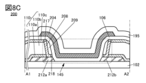
- 8A to 8C are cross-sectional views showing an example of a semiconductor device.
- 9A to 9C are cross-sectional views showing an example of a semiconductor device.
- 10A is a top view illustrating an example of a semiconductor device
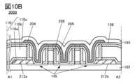
- FIG 10B is a cross-sectional view illustrating the example of the semiconductor device.
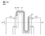
- 11A is a top view illustrating an example of a semiconductor device
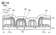
- FIG 11B is a cross-sectional view illustrating the example of the semiconductor device.
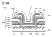
- 12A and 12B are cross-sectional views showing an example of a semiconductor device.
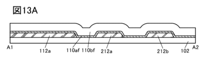
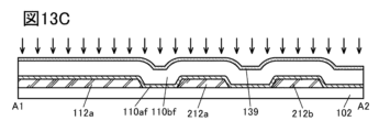
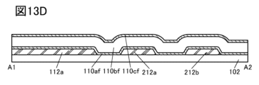
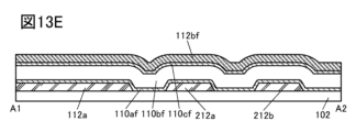
- 13A to 13E are cross-sectional views showing an example of a method for manufacturing a semiconductor device.
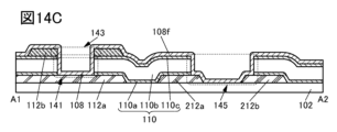
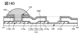
- 14A to 14D are cross-sectional views showing an example of a method for manufacturing a semiconductor device.
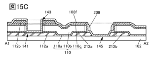
- 15A to 15D are cross-sectional views showing an example of a method for manufacturing a semiconductor device.
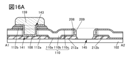
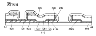
- 16A to 16C are cross-sectional views showing an example of a method for manufacturing a semiconductor device.
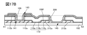
- 17A to 17C are cross-sectional views showing an example of a method for manufacturing a semiconductor device.
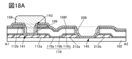
- 18A and 18B are cross-sectional views illustrating an example of a method for manufacturing a semiconductor device.
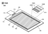
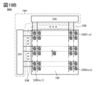
- Fig. 19A is a perspective view showing an example of a display device
- Fig. 19B is a block diagram showing an example of the display device.
- Fig. 20A is a circuit diagram of a latch circuit
- Fig. 20B is a circuit diagram of an inverter circuit.
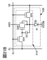
- FIG. 21A and 21B are circuit diagrams of a pixel circuit
- Fig. 21C is a cross-sectional view showing an example of a pixel circuit
- FIG. 22 is a schematic cross-sectional view showing a configuration example of a display device.
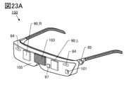
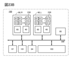
- 23A and 23B are diagrams illustrating an example of the configuration of an electronic device.
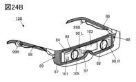
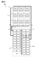
- 24A and 24B are diagrams illustrating an example of the configuration of an electronic device.
- 25A and 25B are diagrams illustrating a configuration example of a display device.
- FIG. 26 is a diagram illustrating an example of the configuration of a display device.
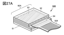
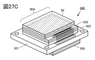
- 27A to 27C are perspective views of a display module.
- 28A and 28B are diagrams illustrating a configuration example of a display device.
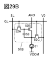
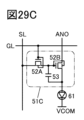
- 29A to 29D are diagrams for explaining a configuration example of a display device.
- 30A to 30D are diagrams illustrating a configuration example of a display device.
- 31A and 31B are diagrams illustrating a configuration example of a display device.
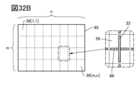
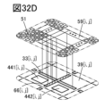
- 32A to 32D are diagrams for explaining a configuration example of a display device.
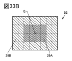
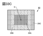
- 33A to 33C are diagrams illustrating a configuration example of a display device.
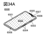
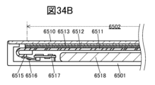
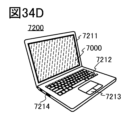
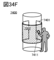
- 34A to 34F are diagrams showing an example of an electronic device.
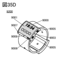
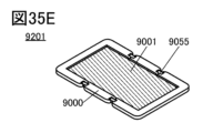
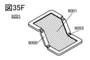
- 35A to 35G are diagrams showing an example of an electronic device.
- Fig. 36A is a diagram for explaining a sub-display section
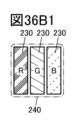
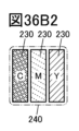
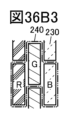
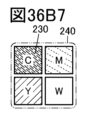
- Figs. 36B1 to 36B7 are diagrams for explaining examples of pixel configurations.
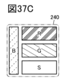
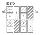
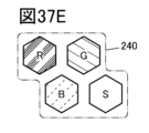
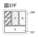
- 37A to 37G are diagrams for explaining examples of pixel configurations.
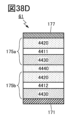
- FIGS. 38A to 38D are diagrams for explaining configuration examples of a light-emitting device.
- Fig. 39A is an optical microscope photograph according to this example
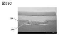
- Fig. 39B and Fig. 39C are cross-sectional STEM images according to this example.
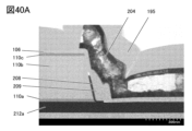
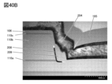
- 40A and 40B are cross-sectional STEM images according to this example.
- FIG. 41 is a diagram showing electrical characteristics according to this embodiment.
- an identification reference number such as “_1”, “[n]”, “[m,n]” may be added to the reference number.
- an identification reference number such as “_1”, “[n]”, “[m,n]” is added to a reference number in a drawing, etc., when it is not necessary to distinguish between them in this specification, the identification reference number may not be added.
- ordinal numbers “first” and “second” are used for convenience and do not limit the number of components or the order of the components (e.g., process order or stacking order). Furthermore, an ordinal number attached to a component in one place in this specification may not match an ordinal number attached to the same component in another place in this specification or in the claims.
- film and “layer” can be interchanged depending on the circumstances.
- conductive layer can be changed to the term “conductive film.”
- insulating film can be changed to the term “insulating layer.”
- a transistor is a type of semiconductor element that can perform functions such as amplifying current or voltage, and switching operations that control conduction or non-conduction.
- transistor includes IGFETs (Insulated Gate Field Effect Transistors) and thin film transistors (TFTs).
- source and drain may be interchanged when transistors of different polarity are used, or when the direction of current changes during circuit operation. For this reason, in this specification and the like, the terms “source” and “drain” may be used interchangeably. Note that the source and drain of a transistor may be appropriately referred to as the source terminal and drain terminal, or the source electrode and drain electrode, depending on the situation.
- Gate and backgate can be used interchangeably. For this reason, in this specification and the like, the terms “gate” and “backgate” can be used interchangeably. Note that the names of the gate and backgate of a transistor can be appropriately changed depending on the situation, such as gate electrode and backgate electrode.
- electrically connected includes cases where the connection is made via "something that has some kind of electrical action.”
- something that has some kind of electrical action is not particularly limited as long as it allows the transmission and reception of electrical signals between the connected objects.
- something that has some kind of electrical action includes electrodes or wiring, as well as switching elements such as transistors, resistive elements, coils, and other elements with various functions.
- the off-state current refers to a leakage current between the source and drain when a transistor is in an off state (also referred to as a non-conducting state or a cut-off state).
- the off-state refers to a state in which the voltage Vgs between the gate and source of an n-channel transistor is lower than the threshold voltage Vth (higher than Vth for a p-channel transistor).
- top surface shapes roughly match means that at least a portion of the contours of the stacked layers overlap. For example, this includes cases where the upper and lower layers are processed using the same mask pattern, or where parts of the mask pattern are the same. However, strictly speaking, the contours may not overlap, and the upper layer may be located inside the lower layer, or outside the lower layer, in which case it may also be said that “top surface shapes roughly match.” Furthermore, when the top surface shapes match or roughly match, it can also be said that the edges are aligned or roughly aligned.
- a tapered shape refers to a shape in which at least a portion of the side of the structure is inclined with respect to the substrate surface or the surface to be formed.
- the side of the structure, the substrate surface, and the surface to be formed do not necessarily need to be completely flat, and may be approximately planar with a slight curvature, or approximately planar with fine irregularities.
- a device manufactured using a metal mask or an FMM may be referred to as a device with an MM (metal mask) structure.
- a device manufactured without using a metal mask or an FMM may be referred to as a device with an MML (metal maskless) structure.
- devices with an MML structure can be manufactured without using a metal mask, they can exceed the upper limit of fineness resulting from the alignment accuracy of the metal mask.
- devices with an MML structure can eliminate the need for equipment related to the manufacture of metal masks and the process of cleaning the metal masks.
- devices with an MML structure are suitable for mass production because they make it possible to keep manufacturing costs low.
- SBS Side By Side
- the SBS structure allows the materials and configuration to be optimized for each light-emitting device, increasing the freedom of material and configuration selection and making it easier to improve brightness and reliability.
- holes or electrons may be referred to as "carriers".
- the hole injection layer or electron injection layer may be referred to as the "carrier injection layer”
- the hole transport layer or electron transport layer may be referred to as the “carrier transport layer”
- the hole block layer or electron block layer may be referred to as the "carrier block layer”.
- the above-mentioned carrier injection layer, carrier transport layer, and carrier block layer may not be clearly distinguishable.
- one layer may have two or three functions among the carrier injection layer, carrier transport layer, and carrier block layer.
- a light-emitting device has an EL layer between a pair of electrodes.
- the EL layer has at least a light-emitting layer.
- layers also called functional layers
- a light-receiving element also called a light-receiving device
- one of the pair of electrodes may be referred to as a pixel electrode, and the other as a common electrode.
- the sacrificial layer (which may also be referred to as a mask layer) is located at least above the light-emitting layer (more specifically, the layer that is processed into an island shape among the layers that make up the EL layer) and has the function of protecting the light-emitting layer during the manufacturing process.
- step discontinuity refers to the phenomenon in which a layer, film, or electrode is divided due to the shape of the surface on which it is formed (e.g., a step, etc.).
- FIG 1A shows a schematic perspective view of a transistor 20.
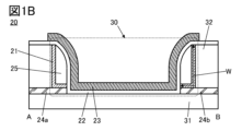
- FIG 1B shows a schematic cross-sectional view taken along dashed line A-B in FIG 1A.
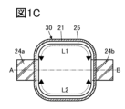
- FIG 1C shows a schematic top view (also referred to as a schematic plan view) of the transistor 20. Note that some components (such as a gate electrode 23, an insulating layer 22, and an insulating layer 25) are omitted in FIG 1A and FIG 1C.
- FIG 1A also shows the source electrode 24a and the drain electrode 24b through the insulating layer 32.
- the transistor 20 is provided on an insulating layer 31 and has a semiconductor layer 21, an insulating layer 22, an insulating layer 25, a gate electrode 23, a source electrode 24a, and a drain electrode 24b.
- the source electrode 24a and the drain electrode 24b are provided on the insulating layer 31. Furthermore, an insulating layer 32 is provided on the insulating layer 31, and the insulating layer 32 has an opening 30 that reaches the insulating layer 31.
- the opening 30 is provided so as to overlap a part of the source electrode 24a and a part of the drain electrode 24b.
- a part of the source electrode 24a and a part of the drain electrode 24b are provided so as to protrude from the side wall of the opening 30 (which may refer to the side surface of the opening 30, or the side surface of the insulating layer 32 in the opening 30).
- the semiconductor layer 21 is provided in contact with the side surface of the insulating layer 32 in the opening 30.
- the insulating layer 25 is provided on the semiconductor layer 21.
- the insulating layer 22 is provided on the semiconductor layer 21, the insulating layer 25, the insulating layer 31, the source electrode 24a, the drain electrode 24b, etc.
- the gate electrode 23 overlaps the opening 30 and is located on the insulating layer 22.
- the semiconductor layer 21 is provided in contact with each of the source electrode 24a and the drain electrode 24b. At least a portion of the semiconductor layer 21 is provided facing the gate electrode 23 via the insulating layer 22 and the insulating layer 25. In other words, the insulating layer 22 and the insulating layer 25 function as a gate insulating layer.
- the semiconductor layer 21 and the insulating layer 25 are provided in a sidewall shape along the periphery of the opening 30 (which can also be called the side surface of the opening 30).
- the stack consisting of the semiconductor layer 21 and the insulating layer 25 provided thereon in contact is provided in a sidewall shape along the periphery of the opening 30.
- the stack can be formed in a sidewall shape by forming it using an anisotropic etching method.
- a protrusion is formed in a portion of the semiconductor layer 21 that contacts the upper surface of a part of the source electrode 24a or a part of the drain electrode 24b.
- the insulating layer 25 is provided on the protrusion of the semiconductor layer 21.
- the protrusion of the semiconductor layer 21 is shaped to protrude toward the center of the opening 30 more than the other portions.
- the semiconductor layer 21 can be said to have a so-called L-shape. Therefore, the insulating layer 25 provided on the protruding portion of the semiconductor layer 21 is surrounded by the semiconductor layer 21 and the insulating layer 22, and does not come into contact with the insulating layer 31, the insulating layer 32, the source electrode 24a, and the drain electrode 24b.
- the insulating layer 25 functions as a hard mask for the semiconductor layer 21.
- the semiconductor layer 21 is covered with the insulating layer 25 when processed into the sidewall shape, so that it is possible to prevent impurities from adhering to the surface of the semiconductor layer 21 (which can also be called the interface between the semiconductor layer 21 and the insulating layer 25). This makes it possible to improve the electrical characteristics and reliability of the transistor 20.
- the semiconductor layer 21 When the semiconductor layer 21 is formed in a sidewall shape, the semiconductor layer 21 contacts a part of the upper surface of the source electrode 24a and a part of the upper surface of the drain electrode 24b. Also, as shown in FIG. 1A, the part of the lower surface of the semiconductor layer 21 that is not in contact with the source electrode 24a and the drain electrode 24b contacts the upper surface of the insulating layer 31. Also, as shown in FIG. 1B, the upper surface of the protruding portion of the semiconductor layer 21 contacts the lower surface of the insulating layer 25. Also, the upper end of the semiconductor layer 21, the side of the protruding portion of the semiconductor layer 21, and the side of the insulating layer 25 on the central side of the opening 30 contact the insulating layer 22. Also, since an area where the semiconductor layer 21 is not provided is formed at the bottom of the opening 30, the insulating layer 22 contacts the insulating layer 31 at the bottom of the opening 30.
- the channel length of the transistor 20 corresponds to the distance between the source electrode 24a and the drain electrode 24b in the circumferential direction of the semiconductor layer 21 provided on the side wall of the opening 30.
- the ring-shaped semiconductor layer 21 is provided over the entire side wall of the opening 30, there are two paths connecting the source electrode 24a and the drain electrode 24b in the semiconductor layer 21, one of which can be the channel length L1, and the other can be the channel length L2.
- the opening 30 is made substantially circular (also called a square shape with rounded corners) and the source electrode 24a and the drain electrode 24b are provided at both ends, so that the channel length L1 and the channel length L2 can be made equal relatively easily.
- the channel width W of the transistor 20 is the sum of the width of the semiconductor layer 21 along the depth direction of the opening 30 and the length of the protruding portion of the semiconductor layer 21.
- the width of the semiconductor layer 21 along the depth direction of the opening 30 can be approximated as the channel width W.
- both paths function as channel formation regions, so that the effective channel width of the transistor 20 may be twice the channel width W.
- the channel width W can be controlled by the thickness of the insulating layer 32 and the depth of the opening 30, a transistor with an extremely short channel width can be realized. For example, it is possible to realize a transistor with an extremely small channel width that could not be realized using exposure equipment for mass production. In addition, it is also possible to realize a transistor with a channel width of less than 10 nm without using the extremely expensive exposure equipment used in cutting-edge LSI technology.
- the channel width W of the transistor can be precisely controlled by the thickness of the insulating layer 32, so that the variation in the channel width W can be made extremely small. Furthermore, a transistor with an extremely small channel width W can be realized.
- the ratio of channel width W to channel length L may be used as an index of transistor characteristics.
- the minimum values of channel length and channel width depend on the exposure limit of an exposure device, so that in order to reduce the W/L ratio, it is necessary to increase L, resulting in a problem of an increase in the area occupied by the transistor.
- the channel width W can be made smaller than the exposure limit of an exposure device, so that a transistor with an extremely small W/L ratio can be realized without increasing the area occupied by the transistor.
- the contour shape of the opening 30 (also referred to as the top surface shape or planar shape) is a square shape with rounded corners, but the present invention is not limited to this.
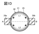
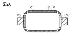
- the contour shape of the opening 30 may be circular as shown in FIG. 1D, or may be rectangular with rounded corners as shown in FIG. 2A.
- the channel length L can be extended.
- the contour shape of the opening 30 circular or approximately circular as shown in FIG. 1C or FIG. 1D, the area occupied by the transistor can be reduced.
- the shape of the opening 30 is simple, the variation in shape can be reduced, and the variation in the electrical characteristics of the transistor can be suppressed.
- the contour shape of the opening 30 is not limited to the above and can be various shapes.
- it can be an ellipse, a rectangle, etc.
- It can also be a regular polygon such as an equilateral triangle, a square, a regular pentagon, or a polygon other than a regular polygon.
- the channel length L can be increased by using a concave polygon such as a star-shaped polygon, which is a polygon with at least one interior angle exceeding 180 degrees.
- it can be a polygon with rounded corners, or a closed curve that combines straight lines and curves.
- the more complex the contour shape of the opening 30 is the greater the channel length L can be.
- the semiconductor layer 21 and insulating layer 25 formed along the side wall of the opening 30 may have a shape in which a part is removed.
- the contour shape of the semiconductor layer 21 and insulating layer 25 shown in FIG. 2A is a closed curve
- the contour shape of the semiconductor layer 21 and insulating layer 25 shown in FIG. 2B is an open curve.
- the entire semiconductor layer 21 can be made into one channel formation region. Therefore, the channel length of the channel formation region of the semiconductor layer 21 shown in FIG. 2B can be made longer than the channel formation region of the semiconductor layer 21 shown in FIG. 2A.
- FIG. 2C also shows an example in which the source electrode 24a and the drain electrode 24b are provided next to each other.
- the semiconductor layer 21 can be provided on most of the sidewall of the opening 30. This allows the channel length L of the transistor to approach the perimeter of the opening 30, and a transistor with a long channel length L can be realized.
- the channel length L is 70% or more, preferably 80% or more, and more preferably 90% or more of the perimeter of the opening 30.
- a configuration in which one transistor is disposed in one opening 30 has been shown, but the present invention is not limited to this.
- a configuration in which two transistors are disposed in one opening 30 may be used.
- the semiconductor layer 21a and the insulating layer 25a, and the semiconductor layer 21b and the insulating layer 25b are provided without contacting each other.
- the transistor 20a having the semiconductor layer 21a and the transistor 20b having the semiconductor layer 21b are provided so as to share one opening 30.
- the transistors 20a and 20b have the same channel width W.
- the transistors 20a and 20b may have different channel lengths L.
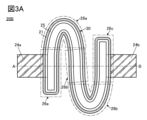
- FIG. 3A is a schematic top view of a transistor 20B.
- Fig. 3B is a schematic cross-sectional view of a cut surface taken along dashed line A-B shown in Fig. 3A. Note that some components (e.g., gate electrode 23, insulating layer 22) are omitted in Fig. 3A.
- transistor 20B differs from transistor 20 shown in configuration example 1 mainly in that opening 30 has a contour shape that includes an extension portion and a bend portion.
- the contour shape of opening 30 formed by combining an extension portion and a bend portion can be called a serpentine shape, a roundabout shape, a meandering shape, or a meandering shape.
- the opening 30 has extension portion 26a, extension portion 26b, extension portion 26c, bend portion 28a, and bend portion 28b.
- the contour shape of the opening 30 can be considered to be a shape in which extension portion 26a and extension portion 26b are connected via bend portion 28a, and extension portion 26b and extension portion 26c are connected via bend portion 28b.
- the semiconductor layer 21 and the insulating layer 25 are provided along the side of the insulating layer 32 in the opening 30. Furthermore, the semiconductor layer 21 has a region in contact with the source electrode 24a and a region in contact with the drain electrode 24b. Furthermore, within the opening 30, the semiconductor layer 21 is provided facing the gate electrode 23 via the insulating layer 22 and the insulating layer 25.
- the semiconductor layer 21 contacts the source electrode 24a at the extension 26a and contacts the drain electrode 24b at the extension 26c.
- the semiconductor layer 21 may also be configured to contact the source electrode 24a or the drain electrode 24b at the bent portion.
- the semiconductor layer 21 may be configured to contact the source electrode 24a at the bent portion 28a and contact the drain electrode 24b at the bent portion 28b.
- a folded structure By connecting two extensions with one bent portion, a folded structure can be formed in the opening 30.
- the length of the opening 30 can be made significantly longer than the distance between the source electrode 24a and the drain electrode 24b. Therefore, the channel length L can be increased without increasing the area occupied by the transistor.
- a transistor with high saturation properties can be obtained.
- a transistor with an extremely small ratio of the channel width W to the channel length L (W/L ratio) can be realized.
- high saturation may be used to refer to a small change in current in the saturation region in the ID-VD characteristics of a transistor.
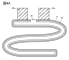
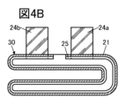
- Figure 4A shows an example of a configuration in which the semiconductor layer 21 is not provided on a portion of the sidewall of the opening 30.
- Figure 4A is a schematic top view.
- FIG. 4A shows an example of a configuration in which the source electrode 24a and the drain electrode 24b are provided adjacent to each other, and further, the semiconductor layer 21 and the insulating layer 25 are not provided on the sidewall of the opening 30 between the source electrode 24a and the drain electrode 24b.
- the channel length L of the transistor can be made closer to the perimeter of the opening 30, and the channel length L can be made longer.
- the opening 30 has extensions 26a, 26b, 26c, bends 28a, and 28b, but the present invention is not limited to this.
- the opening 30 may have multiple extensions and at least one bend. Here, it is preferable that the number of bends is one less than the number of extensions.
- the opening 30 may have two extensions and one bend.
- the opening 30 may have four or more extensions and three or more bends.
- the contour shape of the opening 30 may be a roll shape, as shown in FIG. 4C.
- the semiconductor layer 21 contacts the source electrode 24a and the drain electrode 24b at the extension portion 26a, but this is not a limitation of one aspect of the present invention.
- the semiconductor layer 21 may be configured to contact the source electrode 24a and the drain electrode 24b at the bent portion.
- the semiconductor layer 21 may be configured to contact one of the source electrode 24a and the drain electrode 24b at the bent portion and to contact the other at the extension portion.
- the configuration of the semiconductor layer 21 shown here can also be applied to other configuration examples.
- the corners of the bent portion of the opening 30 are shown as rounded, but this is not a limitation of one aspect of the present invention, and the corners of the bent portion may be angular.
- the contour shape of the opening 30 may be called a zigzag shape.
- the configuration of the opening 30 shown here can also be applied to other configuration examples.
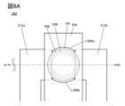
- FIG. 5A A top view (also called a plan view) of the semiconductor device 10 is shown in Fig. 5A.
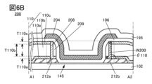
- a cross-sectional view of the cut surface taken along dashed line A1-A2 shown in Fig. 5A is shown in Fig. 5B.
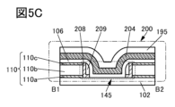
- a cross-sectional view of the cut surface taken along dashed line B1-B2 shown in Fig. 5A is shown in Fig. 5C.
- dashed line B1-B2 is perpendicular to dashed line A1-A2.
- some of the components of the semiconductor device 10 are omitted in Fig. 5A.
- some of the components are omitted in the top views of the semiconductor device in the following drawings.
- the semiconductor device 10 has a transistor 100, a transistor 200, and an insulating layer 110.
- the transistor 100, the transistor 200, and the insulating layer 110 are provided on a substrate 102.
- an insulating layer serving as a base film may be provided on the upper part of the substrate 102.
- the transistor 100, the transistor 200, and the insulating layer 110 are formed on the insulating layer serving as a base film. Therefore, hereinafter, the upper surface of the substrate 102 also includes the upper surface of the insulating layer serving as a base film on the upper part of the substrate 102.
- the insulating layer serving as a base film may be a laminated film of two or more layers.
- Transistor 100 and transistor 200 have different structures. Transistor 100 and transistor 200 can be formed by sharing some of the steps.
- transistor 100 When semiconductor device 10 is applied to a display device, it is preferable to use transistor 100 as a pixel selection transistor and transistor 200 as a driving transistor. More specifically, since it is preferable for the driving transistor to have high saturation, transistor 200 with a long channel length can be preferably used. In this way, the semiconductor device of one embodiment of the present invention has an excellent effect that transistors with different channel lengths can be freely designed on the same substrate by changing the thickness of the insulating layer and pattern formation.
- transistor 200 The configuration of transistor 200 will be explained. Here, an example is shown in which the configuration of transistor 20 described above is applied to transistor 200.
- the transistor 200 includes a conductive layer 204, a conductive layer 212a, a conductive layer 212b, an insulating layer 106, an insulating layer 209, and a semiconductor layer 208.
- the conductive layer 204 functions as a gate electrode
- a part of the insulating layer 106 and a part of the insulating layer 209 function as a gate insulating layer.
- the conductive layer 212a functions as one of a source electrode and a drain electrode
- the conductive layer 212b functions as the other.
- Each layer constituting the transistor 200 may have a single-layer structure or a stacked structure.
- the above-mentioned descriptions regarding the gate electrode 23, the source electrode 24a, the drain electrode 24b, the insulating layer 22, the insulating layer 25, and the semiconductor layer 21 can be referred to.
- the insulating layer 110 has an opening 145.
- a conductive layer 212a and a conductive layer 212b are provided under the insulating layer 110.
- the opening 145 is formed so as to overlap a part of the conductive layer 212a and a part of the conductive layer 212b. It can also be said that the vicinity of the side end of the conductive layer 212a and the vicinity of the side end of the conductive layer 212b protrude from the side wall of the opening 145 (which may refer to the side of the opening 145 or the side of the insulating layer 110 in the opening 145).
- the conductive layer 212a and the conductive layer 212b can be made of the same material.
- the conductive layer 212a and the conductive layer 212b can be formed in the same process.
- the conductive layer 212a and the conductive layer 212b can be formed by forming a film that will become the conductive layer 212a and the conductive layer 212b and processing the film.
- the insulating layer 110 and the opening 145 please refer to the description of the insulating layer 32 and the opening 30 described above.
- the semiconductor layer 208 is provided in contact with a portion of the upper surface of the conductive layer 212a and a portion of the upper surface of the conductive layer 212b. Also, as shown in FIGS. 5A and 5C, the lower surface of the semiconductor layer 208 that is not in contact with the conductive layer 212a and the conductive layer 212b is in contact with the upper surface of the substrate 102. Note that the semiconductor layer 208 is not formed so as to cover the substrate 102 at the bottom of the opening 145. In other words, at least a portion of the bottom of the opening 145 is provided with an area where the semiconductor layer 208 is not formed, and in this area, the upper surface of the substrate 102 and the insulating layer 106 are in contact.
- the region of the semiconductor layer 208 in contact with the conductive layer 212a functions as one of the source region and the drain region, and the region in contact with the conductive layer 212b functions as the other of the source region and the drain region.
- a channel formation region is provided between the source region and the drain region.
- the semiconductor layer 208 and the insulating layer 209 are provided in a sidewall shape along the periphery of the opening 145 (which can also be called the side surface of the opening 145).
- the stack of the semiconductor layer 208 and the insulating layer 209 provided thereon in contact therewith is provided in a sidewall shape along the periphery of the opening 145.
- the stack can be formed in a sidewall shape by forming it using an anisotropic etching method.
- a protrusion is formed on a part of the upper surface of the conductive layer 212a or a part of the semiconductor layer 208 that contacts the upper surface of the conductive layer 212b.
- the insulating layer 209 is provided on the protrusion of the semiconductor layer 208.
- the protrusion of the semiconductor layer 208 is shaped to protrude toward the center of the opening 145 more than the other parts. That is, in the cross-sectional view of the opening 145 as shown in FIG. 5B or FIG. 5C, the semiconductor layer 208 can be said to have a so-called L-shape.
- the insulating layer 209 provided on the protruding portion of the semiconductor layer 208 is surrounded by the semiconductor layer 208 and the insulating layer 106, and does not contact the substrate 102, the insulating layer 110, the conductive layer 212a, and the conductive layer 212b.
- the semiconductor layer 208 is provided in contact with the side wall of the opening 145.
- the lower surface of the insulating layer 209 is in contact with the protruding portion of the semiconductor layer 208.
- the side surface of the insulating layer 209 on the insulating layer 110 side is in contact with the portion of the semiconductor layer 208 along the depth direction of the opening 145.
- the height of the upper end of the semiconductor layer 208 and the height of the upper end of the insulating layer 209 are preferably the same or approximately the same.
- the height of the upper end of the semiconductor layer 208, the height of the upper end of the insulating layer 209, and the height of the upper surface of the insulating layer 110 are preferably the same or approximately the same.
- the lower part of the side surface of the insulating layer 209 on the central side of the opening 145 and the upper part of the side surface of the protruding portion of the semiconductor layer 208 are preferably the same or approximately the same.
- the lower part of the side surface of the protruding portion of the semiconductor layer 208 may be the same or approximately the same as the upper part of the side surface of the conductive layer 212a or the conductive layer 212b.
- the insulating layer 209 functions as a hard mask for the semiconductor layer 208.
- the semiconductor layer 208 is covered with the insulating layer 209 when processed into a sidewall shape, it is possible to prevent impurities from adhering to the surface of the semiconductor layer 208 (which can also be called the interface between the semiconductor layer 208 and the insulating layer 209). This makes it possible to improve the electrical characteristics and reliability of the transistor 200.
- the insulating layer 106 is provided so as to cover the opening 145.
- the semiconductor layer 208 and insulating layer 209 provided inside the opening 145 are also covered by the insulating layer 106.
- the insulating layer 106 is provided on the substrate 102, the semiconductor layer 208, the insulating layer 209, the conductive layer 212a, the conductive layer 212b, and the insulating layer 110.
- the insulating layer 106 has a region in contact with the upper end and side of the protruding portion of the semiconductor layer 208, the side of the insulating layer 209 on the central side of the opening 145, the side near the side end of the conductive layer 212a, the side near the side end of the conductive layer 212b, the side of the insulating layer 110, and the upper surface of the substrate 102.
- the insulating layer 106 has a shape that conforms to the shape of the upper end and side of the protruding portion of the semiconductor layer 208, the side of the insulating layer 209 on the central side of the opening 145, the side near the side end of the conductive layer 212a, the side near the side end of the conductive layer 212b, the side of the insulating layer 110, and the upper surface of the substrate 102. At least a part of the insulating layer 106 and the insulating layer 209 is provided between the semiconductor layer 208 and the conductive layer 204. That is, the insulating layer 106 and the insulating layer 209 function as a gate insulating layer.
- the conductive layer 204 is provided on the insulating layer 106, overlapping the opening 145, and has a region in contact with the upper surface of the insulating layer 106.
- the conductive layer 204 has a region facing the semiconductor layer 208 via the insulating layer 106 and the insulating layer 209.
- the conductive layer 204 has a shape that follows the shape of the upper surface and side surface of the insulating layer 106.
- the transistor 100 has a conductive layer 104, an insulating layer 106, a semiconductor layer 108, a conductive layer 112a, and a conductive layer 112b.
- the conductive layer 104 functions as a gate electrode
- a part of the insulating layer 106 functions as a gate insulating layer.
- the conductive layer 112a functions as one of a source electrode and a drain electrode
- the conductive layer 112b functions as the other.
- Each layer constituting the transistor 100 may have a single-layer structure or a stacked structure.
- a conductive layer 112a is provided on the substrate 102, and an insulating layer 110 is provided on the conductive layer 112a.
- the insulating layer 110 is provided so as to cover the upper surface and side surfaces of the conductive layer 112a.
- the insulating layer 110 has an opening 141 that reaches the conductive layer 112a in a region overlapping with the conductive layer 112a. It can also be said that the conductive layer 112a is exposed in the opening 141.
- the conductive layer 112a can be formed using the same material as the conductive layer 212a and the conductive layer 212b. In addition, the conductive layer 112a can be formed in the same process as the conductive layer 212a and the conductive layer 212b.
- the conductive layer 112a, the conductive layer 212a, and the conductive layer 212b can be formed by forming a film that will become the conductive layer 112a, the conductive layer 212a, and the conductive layer 212b, and processing the film.
- the tapered shapes of the side ends of the conductive layer 112a, the conductive layer 212a, and the conductive layer 212b may be similar.
- a conductive layer 112b is provided on the insulating layer 110.
- the conductive layer 112b has an area that overlaps with the conductive layer 112a via the insulating layer 110.
- the conductive layer 112b has an opening 143 in the area that overlaps with the conductive layer 112a.
- the opening 143 is provided in the area that overlaps with the opening 141.
- the semiconductor layer 108 is provided so as to cover the openings 141 and 143.
- the same material as the semiconductor layer 208 can be used for the semiconductor layer 108.
- the semiconductor layer 108 can be formed in the same process as the semiconductor layer 208.
- the semiconductor layer 108 and the semiconductor layer 208 can be formed by forming a film that will become the semiconductor layer 108 and the semiconductor layer 208 and processing the film.
- the semiconductor layer 108 has a region in contact with the upper surface and side surfaces of the conductive layer 112b, the side surfaces of the insulating layer 110, and the upper surface of the conductive layer 112a.
- the semiconductor layer 108 is electrically connected to the conductive layer 112a through the openings 141 and 143.
- the semiconductor layer 108 has a shape that conforms to the shapes of the upper surface and side surfaces of the conductive layer 112b, the side surfaces of the insulating layer 110, and the upper surface of the conductive layer 112a.
- the semiconductor layer 108 has a region that overlaps with the conductive layer 112a through the insulating layer 110. It can also be said that the insulating layer 110 has a region that is sandwiched between the conductive layer 112a and the semiconductor layer 108.
- the region of the semiconductor layer 108 in contact with the conductive layer 112a functions as one of the source region and the drain region, and the region in contact with the conductive layer 112b functions as the other of the source region and the drain region.
- a channel formation region is provided between the source region and the drain region.
- the insulating layer 106 is provided so as to cover the openings 141 and 143.
- the insulating layer 106 is provided on the semiconductor layer 108, the conductive layer 112b, and the insulating layer 110.
- the insulating layer 106 has an area that contacts the upper surface and side surfaces of the semiconductor layer 108, the upper surface and side surfaces of the conductive layer 112b, and the upper surface of the insulating layer 110.
- the insulating layer 106 has a shape that follows the shapes of the upper surface and side surfaces of the semiconductor layer 108, the upper surface and side surfaces of the conductive layer 112b, and the upper surface of the insulating layer 110.
- the conductive layer 104 is provided on the insulating layer 106 and has a region in contact with the upper surface of the insulating layer 106.
- the conductive layer 104 has a region that overlaps with the semiconductor layer 108 through the insulating layer 106.
- the conductive layer 104 has a shape that matches the shapes of the upper surface and side surface of the insulating layer 106.
- the conductive layer 104 can be formed using the same material as the conductive layer 204.
- the conductive layer 104 can be formed in the same process as the conductive layer 204.
- the conductive layer 104 and the conductive layer 204 can be formed by forming a film that will become the conductive layer 104 and the conductive layer 204 and processing the film.
- the transistor 100 is a so-called top-gate transistor having a gate electrode above the semiconductor layer 108. Furthermore, since the bottom surface of the semiconductor layer 108 is in contact with the conductive layer 112a and the conductive layer 112b that function as a source electrode and a drain electrode, the transistor 100 can be called a TGBC (Top Gate Bottom Contact) type transistor.
- the source electrode and the drain electrode of the transistor 100 are located at different heights with respect to the surface of the substrate 102, which is the surface on which the transistor 100 is formed, and the drain current flows in a direction perpendicular to or approximately perpendicular to the surface of the substrate 102. It can also be said that the drain current flows vertically or approximately vertically in the transistor 100.
- the transistor that is one embodiment of the present invention can be called a vertical channel transistor or a VFET (Vertical Field Effect Transistor).
- transistor 200 is configured to allow current to flow both vertically and horizontally, it can be called a VLFET (Vertical Lateral Field Effect Transistor).
- the channel length of the transistor 100 can be controlled by the thickness of the insulating layer 110 (specifically, the insulating layer 110b) provided between the conductive layer 112a and the conductive layer 112b. Therefore, a transistor having a channel length shorter than the limit resolution of an exposure device used to manufacture the transistor can be manufactured with high precision.
- the characteristic variation between multiple transistors 100 is also reduced. This makes it possible to stabilize the operation of a semiconductor device including the transistor 100 and to increase its reliability.
- the reduced characteristic variation increases the degree of freedom in circuit design and allows the operating voltage of the semiconductor device to be reduced. This allows the power consumption of the semiconductor device to be reduced.
- the transistor 100 can have a source electrode, a layer having a channel formation region, and a drain electrode stacked on top of each other, so the area it occupies can be significantly reduced compared to a so-called planar type transistor in which the layer having the channel formation region is arranged in a planar shape.
- the conductive layer 112a, the conductive layer 112b, and the conductive layer 104 can each function as wiring, and the transistor 100 can be provided in a region where these wirings overlap. That is, in a circuit having the transistor 100 and the wiring, the area occupied by the transistor 100 and the wiring can be reduced. Therefore, the area occupied by the circuit can be reduced, and a small-sized semiconductor device can be obtained.
- the transistor 100 with a short channel length and the transistor 200 with a long channel length can be formed on the same substrate by sharing some of the processes.
- a high-performance semiconductor device can be obtained by applying the transistor 100 to a transistor that requires a large on-state current and the transistor 200 to a transistor that requires high saturation.
- the conductive layer 112a and the conductive layer 112b functioning as the source electrode and the drain electrode of the transistor 100 are provided on different surfaces. Specifically, the conductive layer 112a is provided on the substrate 102, the conductive layer 112b is provided on the insulating layer 110, and the insulating layer 110 is sandwiched between the conductive layer 112a and the conductive layer 112b.
- the conductive layer 212a and the conductive layer 212b functioning as the source electrode and the drain electrode of the transistor 200 are provided on the same surface. Specifically, the conductive layer 212a and the conductive layer 212b are provided on the substrate 102. It can also be said that one of the source electrode and the drain electrode of the transistor 100 is provided on a surface different from the source electrode and the drain electrode of the transistor 200, and the other is provided on the same surface as the source electrode and the drain electrode of the transistor 200.
- a semiconductor device of one embodiment of the present invention when a semiconductor device of one embodiment of the present invention is applied to a pixel circuit of a display device, the area occupied by the pixel circuit can be reduced, and a high-definition display device can be obtained.
- a semiconductor device of one embodiment of the present invention when a semiconductor device of one embodiment of the present invention is applied to a driver circuit of a display device (e.g., one or both of a gate line driver circuit and a source line driver circuit), the area occupied by the driver circuit can be reduced, and a display device with a narrow frame can be obtained.
- An insulating layer 195 is provided to cover the transistors 100 and 200.
- the insulating layer 195 functions as a protective layer for the transistors 100 and 200.
- transistor 100 and transistor 200 Next, the detailed configuration of transistor 100 and transistor 200 will be described.
- the semiconductor layer 108 and the semiconductor layer 208 each have a metal oxide (also called an oxide semiconductor) that exhibits semiconductor properties.
- a metal oxide also called an oxide semiconductor
- the band gap of the metal oxide used in the semiconductor layer 108 and the semiconductor layer 208 is preferably 2.0 eV or more, and more preferably 2.5 eV or more.
- OS transistors have extremely high field-effect mobility compared to transistors using amorphous silicon.
- OS transistors have an extremely small off-state current and can hold charge accumulated in a capacitor connected in series with the transistor for a long period of time.
- the use of OS transistors can reduce the power consumption of a semiconductor device.
- the crystallinity of the semiconductor material used for the semiconductor layer 108 and the semiconductor layer 208 is not particularly limited, and any of an amorphous semiconductor, a single crystal semiconductor, and a semiconductor having crystallinity other than single crystal (a microcrystalline semiconductor, a polycrystalline semiconductor, or a semiconductor having a crystalline region in part) may be used.
- the use of a single crystal semiconductor or a semiconductor having crystallinity is preferable because it can suppress deterioration of the transistor characteristics.
- the semiconductor material used for the semiconductor layer 108 and the semiconductor layer 208 is not particularly limited.
- a semiconductor made of a single element or a compound semiconductor can be used.
- semiconductors made of a single element include silicon and germanium.
- compound semiconductors include gallium arsenide and silicon germanium.
- Other examples of compound semiconductors include organic semiconductors, nitride semiconductors, and oxide semiconductors (OS: oxide semiconductor). Note that these semiconductor materials may contain impurities as dopants.
- the semiconductor layer 108 and the semiconductor layer 208 can each be made of silicon.
- silicon examples include single crystal silicon, polycrystalline silicon, microcrystalline silicon, and amorphous silicon.
- polycrystalline silicon examples include low temperature polysilicon (LTPS).
- Transistors using amorphous silicon in the channel formation region can be formed on a large glass substrate and can be manufactured at low cost. Transistors using polycrystalline silicon in the channel formation region have high field effect mobility and can operate at high speed. Furthermore, transistors using microcrystalline silicon in the channel formation region have higher field effect mobility and can operate at high speed than transistors using amorphous silicon.
- the insulating layer 110 preferably has one or more inorganic insulating films.
- materials that can be used for the inorganic insulating film include oxides, nitrides, oxynitrides, and nitride oxides.
- oxides include silicon oxide, aluminum oxide, magnesium oxide, gallium oxide, germanium oxide, yttrium oxide, zirconium oxide, lanthanum oxide, neodymium oxide, hafnium oxide, tantalum oxide, cerium oxide, gallium zinc oxide, and hafnium aluminate.
- nitrides include silicon nitride and aluminum nitride.
- Examples of oxynitrides include silicon oxynitride, aluminum oxynitride, gallium oxynitride, yttrium oxynitride, and hafnium oxynitride.
- Examples of nitride oxides include silicon nitride oxide and aluminum nitride oxide.
- an oxynitride refers to a material whose composition contains more oxygen than nitrogen.
- a nitride oxide refers to a material whose composition contains more nitrogen than oxygen.
- silicon oxynitride refers to a material whose composition contains more oxygen than nitrogen.
- Silicon nitride oxide refers to a material whose composition contains more nitrogen than oxygen.
- the region of the semiconductor layer 208 in contact with the insulating layer 110 functions as a channel formation region.
- the region of the semiconductor layer 108 in contact with the insulating layer 110 functions as a channel formation region.
- the region of the insulating layer 110 in contact with the channel formation region of the semiconductor layer 108 and the region in contact with the channel formation region of the semiconductor layer 208 contain oxygen.
- One or more of an oxide and an oxynitride can be suitably used for the region of the insulating layer 110 in contact with the channel formation region of the semiconductor layer 108 and the region in contact with the channel formation region of the semiconductor layer 208.
- the insulating layer 110 preferably has a laminated structure.
- FIG. 5B and other figures show an example in which the insulating layer 110 has an insulating layer 110a, an insulating layer 110b on the insulating layer 110a, and an insulating layer 110c on the insulating layer 110b.
- FIGS. 6A and 6B show enlarged views of the transistor 200 shown in FIG. 5A and FIG. 5B.
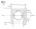
- FIGS. 7A and 7B show enlarged views of the transistor 100.
- the insulating layer 110b preferably contains oxygen, and preferably uses one or more of the oxides and oxynitrides described above. Specifically, one or both of silicon oxide and silicon oxynitride can be preferably used for the insulating layer 110b. Thus, at least the region of the semiconductor layer 208 in contact with the insulating layer 110b and the region of the semiconductor layer 108 in contact with the insulating layer 110b can each function as a channel formation region.
- a film that releases oxygen when heated for the insulating layer 110b It is more preferable to use a film that releases oxygen when heated for the insulating layer 110b.
- the insulating layer 110b releases oxygen, so that oxygen can be supplied to the semiconductor layer 108.
- oxygen vacancies (V O ) are repaired, and the oxygen vacancies (V O ) can be reduced.
- defects in which hydrogen has entered the oxygen vacancies (V O ) (hereinafter also referred to as V O H) can be reduced by supplying oxygen. Therefore, a transistor that exhibits good electrical characteristics and is highly reliable can be obtained.
- oxygen can be supplied to the insulating layer 110b by performing heat treatment in an oxygen-containing atmosphere or plasma treatment in an oxygen-containing atmosphere.
- oxygen may be supplied to the insulating layer 110b by forming an oxide film in an oxygen-containing atmosphere on the upper surface of the insulating layer 110b by a sputtering method. The oxide film may then be removed. Note that in the third embodiment described later, an example of supplying oxygen to the insulating layer 110b by forming a metal oxide layer 137 is shown.
- the insulating layer 110b is preferably formed by a deposition method such as a sputtering method or a plasma enhanced chemical vapor deposition (PECVD) method.
- a deposition method such as a sputtering method or a plasma enhanced chemical vapor deposition (PECVD) method.
- PECVD plasma enhanced chemical vapor deposition
- the insulating layer 110b it is preferable that substances (e.g., atoms, molecules, and ions) diffuse easily. It can also be said that it is preferable that the diffusion coefficient of the substance in the insulating layer 110b is large. In particular, it is preferable that oxygen diffuses easily in the insulating layer 110b. In other words, it is preferable that the diffusion coefficient of oxygen in the insulating layer 110b is large.
- the oxygen contained in the insulating layer 110b diffuses through the insulating layer 110b and is supplied to the semiconductor layer 108 via the interface between the insulating layer 110b and the semiconductor layer 108, and is also supplied to the semiconductor layer 208 via the interface between the insulating layer 110b and the semiconductor layer 208.
- V O oxygen vacancies
- V O H increases due to an increase in oxygen vacancies (V O ) in the channel formation region, which may shift the threshold voltage of the transistor and increase the drain current (hereinafter also referred to as cutoff current) that flows when the gate voltage is 0 V.
- cutoff current may increase due to a shift in the threshold voltage to the negative side.
- oxygen is supplied to at least the region of the semiconductor layer 108 that is in contact with the insulating layer 110b and the region of the semiconductor layer 208 that is in contact with the insulating layer 110b, that is, the channel formation regions of the transistors 100 and 200, and the oxygen vacancies (V O ) and V O H in the channel formation regions can be reduced.
- V O oxygen vacancies
- V O H oxygen vacancies
- the region of the semiconductor layer 108 in contact with the conductive layer 112a functions as one of the source and drain regions of the transistor 100, and the region in contact with the conductive layer 112b functions as the other.
- the source and drain regions are regions with lower electrical resistance than the channel formation region.
- the source and drain regions can also be said to be regions with a higher carrier concentration and a higher oxygen defect density than the channel formation region.
- the insulating layer 110a is provided between the insulating layer 110b and the conductive layer 112a.
- the insulating layer 110c is provided between the insulating layer 110b and the conductive layer 112b. It is preferable that the insulating layer 110a and the insulating layer 110c each release a small amount of impurities (e.g., hydrogen and water) and are difficult for the impurities to permeate. This can prevent the impurities contained in the insulating layer 110a and the insulating layer 110c from diffusing into the channel formation region. Therefore, it is possible to obtain a transistor that exhibits good electrical characteristics and is highly reliable.
- impurities e.g., hydrogen and water
- the insulating layer 110a and the insulating layer 110c are preferably made of a film that is difficult for oxygen to permeate. This can suppress the oxygen contained in the insulating layer 110b from diffusing to the conductive layer 112a through the insulating layer 110a. Similarly, the oxygen contained in the insulating layer 110b can be suppressed from diffusing to the conductive layer 112b through the insulating layer 110c. This can suppress the conductive layer 112a and the conductive layer 112b from being oxidized and their electrical resistance from increasing. In addition, the amount of oxygen supplied from the insulating layer 110b to the channel formation region is increased, and oxygen vacancies (V O ) and V O H in the channel formation region can be reduced.
- oxygen can be effectively supplied from the insulating layer 110b to the channel formation region.
- a configuration in which one or both of the insulating layers 110a and 110c are not provided may also be used.
- the insulating layer 110a and the insulating layer 110c each preferably contain nitrogen, and preferably use one or more of the above-mentioned nitrides and nitride oxides.
- silicon nitride or silicon nitride oxide may be preferably used for the insulating layer 110a and the insulating layer 110c.
- one or both of the insulating layer 110a and the insulating layer 110c may use one or more of an oxide and an oxynitride.
- aluminum oxide may be preferably used for the insulating layer 110a and the insulating layer 110c.
- the insulating layer 110a may use the same material as the insulating layer 110c, or a different material.
- different materials refer to materials in which some or all of the constituent elements are different, or materials in which the constituent elements are the same but the composition is different.
- the thickness T110a of the insulating layer 110a can be, for example, 3 nm or more, 5 nm or more, 10 nm or more, 20 nm or more, 50 nm or more, or 70 nm or more, and can be less than 1 ⁇ m, 500 nm or less, 400 nm or less, 300 nm or less, 200 nm or less, 150 nm or less, or 120 nm or less. As shown in FIG. 7B, the thickness T110a can be the shortest distance between the surface on which the insulating layer 110a is formed (here, the upper surface of the conductive layer 112a) and the lower surface of the insulating layer 110b in a cross-sectional view.
- the thickness T110a of the insulating layer 110a When the thickness T110a of the insulating layer 110a is large, the amount of impurities released from the insulating layer 110a increases, and the amount of impurities diffusing into the channel formation region may increase. On the other hand, when the thickness T110a is small, oxygen contained in the insulating layer 110b may diffuse to the conductive layer 112a side through the insulating layer 110a, and the amount of oxygen supplied to the channel formation region may decrease. By setting the thickness T110a within the above range, oxygen vacancies (V O ) and V O H in the channel formation region can be reduced. In addition, the conductive layer 112a is oxidized by the oxygen contained in the insulating layer 110b, and the electrical resistance of the conductive layer 112a can be prevented from increasing.
- the thickness T110c of the insulating layer 110c can be, for example, 3 nm or more, 5 nm or more, 10 nm or more, 15 nm or more, or 20 nm or more, and can be 1 ⁇ m or less, 500 nm or less, 300 nm or less, 200 nm or less, 150 nm or less, 120 nm or less, or 100 nm or less. As shown in FIG. 7B, the thickness T110c can be the shortest distance between the surface on which the insulating layer 110c is formed (here, the upper surface of the insulating layer 110b) and the lower surface of the conductive layer 112b in a cross-sectional view.
- the thickness T110c of the insulating layer 110c When the thickness T110c of the insulating layer 110c is large, the amount of impurities released from the insulating layer 110c increases, and the amount of impurities diffusing into the channel formation region may increase. On the other hand, when the thickness T110c is small, oxygen contained in the insulating layer 110b may diffuse to the conductive layer 112b side through the insulating layer 110c, and the amount of oxygen supplied to the channel formation region may decrease. By setting the thickness T110c within the above range, oxygen vacancies (V O ) and V O H in the channel formation region can be reduced. In addition, the conductive layer 112b is oxidized by the oxygen contained in the insulating layer 110b, and the electrical resistance of the conductive layer 112b can be prevented from increasing.
- At least one of the region of the semiconductor layer 108 in contact with the insulating layer 110a and the region of the semiconductor layer 108 in contact with the insulating layer 110c may be a region having a lower electrical resistance than the channel formation region (hereinafter, also referred to as a low-resistance region).
- the region may be a region having a higher carrier concentration or a higher oxygen defect density than the channel formation region.
- the semiconductor layer 108 can be configured to have a low-resistance region between the region in contact with the conductive layer 112a (one of the source region and the drain region) and the channel formation region. Similarly, by using a material that releases impurities in the insulating layer 110c, the region of the semiconductor layer 108 in contact with the insulating layer 110c can be a low-resistance region.
- the semiconductor layer 108 can be configured to have a low-resistance region between the region in contact with the conductive layer 112b (the other of the source region and the drain region) and the channel formation region.
- the low resistance regions can function as buffer regions to reduce the drain electric field. These low resistance regions may also function as source or drain regions.
- the conductive layer 112a functions as a drain electrode and the conductive layer 112b functions as a source electrode, by making the region of the semiconductor layer 108 in contact with the insulating layer 110a into a low resistance region, a high electric field is unlikely to occur near the drain region, the generation of hot carriers is suppressed, and deterioration of the transistor can be suppressed.
- the conductive layer 112a functions as a source electrode and the conductive layer 112b functions as a drain electrode, by making the region of the semiconductor layer 108 in contact with the insulating layer 110c into a low resistance region, a high electric field is unlikely to occur near the drain region, the generation of hot carriers is suppressed, and deterioration of the transistor can be suppressed.
- the region of the semiconductor layer 208 in contact with the insulating layer 110a may be a low resistance region compared to the channel formation region.
- This region can also be said to be a region with a high carrier concentration or a high oxygen defect density compared to the channel formation region.
- impurities e.g., water or hydrogen
- the region in contact with the insulating layer 110a can be made into a low resistance region.
- the semiconductor layer 208 can be configured to have a low resistance region between the region in contact with the conductive layer 212a (one of the source region and the drain region) and the channel formation region.
- the low resistance region can function as a buffer region for relaxing the drain electric field. Note that the low resistance region may function as a source region or a drain region.
- the amount of impurities released from the insulating layers 110a and 110c is too large, the impurities may diffuse into the channel formation region. Even if a material that releases impurities is used for the insulating layers 110a and 110c, it is preferable that the amount of released impurities is small.
- the insulating layer 110 has at least the insulating layer 110b.
- the insulating layer 110 may not have one or both of the insulating layer 110a and the insulating layer 110c.
- the insulating layer 110 may have a stacked structure of two layers, four or more layers, or a single layer structure.
- the top surface shapes of the openings 145, 141, and 143 are not limited, and may be, for example, a circle, an ellipse, a triangle, a quadrangle (including a rectangle, a diamond, and a square), a pentagon, or other polygonal shape, or a shape with rounded corners of these polygons.
- the polygon may be either a concave polygon (a polygon with at least one interior angle exceeding 180 degrees) or a convex polygon (a polygon with all interior angles less than 180 degrees).
- it is preferable that the top surface shapes of the openings 141 and 143 are each circular. By making the top surface shapes of the openings circular, the processing accuracy when forming the openings can be improved, and openings of a fine size can be formed.
- a circle is not limited to a perfect circle.
- the top surface shape of the opening 145 is circular, but the present invention is not limited to this, and various shapes are possible as described above.
- the top surface shape of opening 145 refers to the shape of the top surface end portion of insulating layer 110 on the opening 145 side.
- the top surface shape of opening 141 refers to the shape of the top surface end portion of insulating layer 110 on the opening 141 side.
- the top surface shape of opening 143 refers to the shape of the bottom surface end portion of conductive layer 112b on the opening 143 side.
- the top surface shapes of openings 141 and 143 can be made to match or roughly match each other.
- the bottom surface end of conductive layer 112b on the opening 143 side match or roughly match the top surface end of insulating layer 110 on the opening 141 side.
- the bottom surface of conductive layer 112b refers to the surface on the insulating layer 110 side.
- the top surface of insulating layer 110 refers to the surface on the conductive layer 112b side.
- openings 141 and 143 can be viewed together as a single opening.
- openings 141 and 143 do not have to be the same. Furthermore, when the top surface shapes of openings 141 and 143 are circular, openings 141 and 143 may or may not be concentric.
- the channel length L100 of the transistor 100 is indicated by a double-headed dashed arrow.
- the channel length L100 of the transistor 100 corresponds to the length of the side of the insulating layer 110b on the opening 141 side in a cross-sectional view.
- the channel length L100 is determined by the thickness T110b of the insulating layer 110b and the angle ⁇ 110 between the side of the insulating layer 110b on the opening 141 side and the surface on which the insulating layer 110b is to be formed (here, the upper surface of the insulating layer 110a). Therefore, the channel length L100 can be set to a value smaller than the limit resolution of the exposure device, and a transistor of a fine size can be realized.
- a transistor with an extremely small channel length that could not be realized with a conventional exposure device for mass production of flat panel displays (for example, a minimum line width of about 2 ⁇ m or 1.5 ⁇ m).
- a transistor with a channel length of less than 10 nm without using an extremely expensive exposure device used in cutting-edge LSI technology.
- the channel length L100 can be, for example, 5 nm or more, 7 nm or more, or 10 nm or more, and less than 3 ⁇ m, 2.5 ⁇ m or less, 2 ⁇ m or less, 1.5 ⁇ m or less, 1.2 ⁇ m or less, 1 ⁇ m or less, 500 nm or less, 300 nm or less, 200 nm or less, 100 nm or less, 50 nm or less, 30 nm or less, or 20 nm or less.
- the channel length L100 can be 100 nm or more and 1 ⁇ m or less.
- the on-state current of the transistor 100 can be increased.
- the transistor 100 By using the transistor 100, a circuit capable of high-speed operation can be manufactured. Furthermore, the area occupied by the circuit can be reduced. Therefore, a small-sized semiconductor device can be obtained. For example, when the semiconductor device of one embodiment of the present invention is applied to a large display device or a high-definition display device, even if the number of wirings is increased, signal delay in each wiring can be reduced and display unevenness can be suppressed. Furthermore, since the area occupied by the circuit can be reduced, the frame of the display device can be narrowed.
- the channel length L100 can be controlled by adjusting the thickness T110b and angle ⁇ 110 of the insulating layer 110b. Note that in FIG. 7B, the thickness T110b of the insulating layer 110b is indicated by a double-headed arrow of a dashed line.
- the thickness T110b of the insulating layer 110b can be, for example, 5 nm or more, 7 nm or more, or 10 nm or more, and less than 3 ⁇ m, 2.5 ⁇ m or less, 2 ⁇ m or less, 1.5 ⁇ m or less, 1.2 ⁇ m or less, 1 ⁇ m or less, 500 nm or less, 300 nm or less, 200 nm or less, 100 nm or less, 50 nm or less, 30 nm or less, or 20 nm or less.
- the side of the insulating layer 110 on the opening 141 side can also be tapered.
- the angle ⁇ 110 is preferably 90 degrees or less.
- the coverage of the layer (e.g., semiconductor layer 108) formed on the insulating layer 110 can be improved.
- the angle ⁇ 110 can be, for example, 30 degrees or more, 35 degrees or more, 40 degrees or more, 45 degrees or more, 50 degrees or more, 55 degrees or more, 60 degrees or more, 65 degrees or more, or 70 degrees or more, and 90 degrees or less, 85 degrees or less, or 80 degrees or less.
- the angle ⁇ 110 may also be 75 degrees or less, 70 degrees or less, 65 degrees or less, or 60 degrees or less.
- the shape of the side of the insulating layer 110 on the opening 141 side is shown as straight lines in cross section, but this is not a limitation of one embodiment of the present invention. In cross section, the shape of the side of the insulating layer 110 on the opening 141 side may be curved, or the side may have both straight and curved regions.
- the conductive layer 112b is not provided inside the opening 141. Specifically, it is preferable that the conductive layer 112b does not have a region that is in contact with the side surface of the insulating layer 110 on the opening 141 side. If the conductive layer 112b is also provided inside the opening 141, the channel length L100 of the transistor 100 becomes shorter than the length of the side surface of the insulating layer 110b, which may make it difficult to control the channel length L100. Therefore, it is preferable that the top shape of the opening 143 matches the top shape of the opening 141, or that the opening 143 encompasses the opening 141 in a top view (also referred to as a plan view).
- the width D141 of opening 141 is indicated by a double-headed arrow with a dashed two-dot line.
- Figure 7A shows an example in which the top surface shape of opening 141 is circular.
- width D141 corresponds to the diameter of the circle
- channel width W100 of transistor 100 is the circumference of the circle.
- channel width W100 is ⁇ x D141.
- the width D141 of the opening 141 may vary in the depth direction.
- the width D141 of the opening 141 may be the average value of the diameter at the highest point of the insulating layer 110b (or insulating layer 110) in a cross-sectional view, the diameter at the lowest point, and the diameter at the midpoint between these three diameters.
- the diameter of the opening 141 may be any of the diameters at the highest point of the insulating layer 110b (or insulating layer 110) in a cross-sectional view, the diameter at the lowest point, and the diameter at the midpoint between these three diameters.
- the width D141 of the opening 141 is equal to or greater than the limit resolution of the exposure device.
- the width D141 can be, for example, 200 nm or more, 300 nm or more, 400 nm or more, or 500 nm or more, and less than 5 ⁇ m, 4.5 ⁇ m or less, 4 ⁇ m or less, 3.5 ⁇ m or less, 3 ⁇ m or less, 2.5 ⁇ m or less, 2 ⁇ m or less, 1.5 ⁇ m or less, or 1 ⁇ m or less.
- the insulating layer 110a and the insulating layer 110c are made of a material that releases less hydrogen.
- the insulating layer 110a and the insulating layer 110c are made of a material that releases even a small amount of hydrogen, it is preferable that the thicknesses of these layers are thin.
- the thickness T110a of the insulating layer 110a and the thickness T110c of the insulating layer 110c are 1 nm or more, 3 nm or more, or 5 nm or more, and preferably 50 nm or less, 40 nm or less, 30 nm or less, 20 nm or less, 15 nm or less, or 10 nm or less. This makes it possible to reduce the amount of impurities that diffuse into the channel formation region, and to provide a transistor that exhibits good electrical characteristics and is highly reliable even when the channel length L100 is short.
- the region of the semiconductor layer 108 in contact with the insulating layer 110b functions as a channel formation region
- one embodiment of the present invention is not limited to this.
- the region of the semiconductor layer 108 in contact with the insulating layer 110a may also function as a channel formation region.
- the region in contact with the insulating layer 110c may also function as a channel formation region.
- a step may be formed between the insulating layer 110 and the conductive layer 112a, and the semiconductor layer 108, the insulating layer 106, and the conductive layer 104 may be provided along the step.
- the semiconductor layer 108 and the insulating layer 109 may be provided in a sidewall shape along the sidewalls of the openings 141 and 143 in the transistor 100.
- the semiconductor layer 108 has the same shape as the semiconductor layer 208
- the insulating layer 109 has the same shape as the insulating layer 209.
- the insulating layer 109 can be formed in the same process as the insulating layer 209, so that the insulating layer 109 and the insulating layer 109 have the same insulating material.
- the upper part of the semiconductor layer 108 contacts the side surface of the conductive layer 112b, which is the sidewall of the opening 143.
- the lower surface of the semiconductor layer 108 contacts the upper surface of the conductive layer 112a.
- at least a part of the semiconductor layer 108 faces the conductive layer 104 through the insulating layer 109 and the insulating layer 106. That is, the insulating layer 109 and the insulating layer 106 function as the gate insulating layer of the transistor 100.
- the transistor 100 may be configured such that an insulating layer 109 is provided further inside the semiconductor layer 108 provided inside the openings 141 and 143. That is, the transistor 100 shown in FIG. 7B may be configured such that an insulating layer 109 is further provided.
- the transistor 100 at least a part of the semiconductor layer 108 faces the conductive layer 104 via the insulating layer 109 and the insulating layer 106. That is, the insulating layer 109 and the insulating layer 106 function as the gate insulating layer of the transistor 100.
- the channel length L200a and the channel length L200b of the transistor 200 are indicated by solid double-headed arrows.
- the channel length L200a and the channel length L200b correspond to the distance between the conductive layer 212a and the conductive layer 212b along the circumferential direction of the semiconductor layer 208 provided on the side wall of the opening 145.
- the annular semiconductor layer 208 is provided over the entire side wall of the opening 145, so that there are two paths connecting the conductive layer 212a and the conductive layer 212b in the semiconductor layer 208, one of which can be the channel length L200a and the other can be the channel length L200b.
- the channel length L200a and the channel length L200b are equal or approximately equal.
- the conductive layer 212a and the conductive layer 212b are arranged symmetrically with respect to the opening 145.
- the channel length L200a and the channel length L200b can be made equal.
- the channel length L200a and the channel length L200b of the transistor 200 can be controlled by the top surface shape and size of the opening 145. Therefore, the channel length L200a and the channel length L200b can be made greater than the channel length L100.
- the channel width W200 of the transistor 200 is indicated by a double-headed dashed arrow.
- the channel width W200 is the sum of the width of the semiconductor layer 208 along the depth direction of the opening 145 and the length of the protruding portion of the semiconductor layer 208.
- the protruding portion of the semiconductor layer 208 is sufficiently smaller than the width of the semiconductor layer 208 along the depth direction of the opening 145, the width of the semiconductor layer 208 along the depth direction of the opening 145 can be approximated to the channel width W200.
- both paths function as channel formation regions, so that the effective channel width of the transistor 200 may be twice the channel width W200.
- the channel width W200 of the transistor 200 can be controlled by the thickness of the insulating layer 110 (particularly the thickness of the insulating layer 110b).
- the channel width W200 of the transistor 200 can be made into a very fine structure below the exposure limit of photolithography.
- the channel width W200 can be, for example, 5 nm or more, 7 nm or more, or 10 nm or more, and less than 3 ⁇ m, 2.5 ⁇ m or less, 2 ⁇ m or less, 1.5 ⁇ m or less, 1.2 ⁇ m or less, 1 ⁇ m or less, 500 nm or less, 300 nm or less, 200 nm or less, 100 nm or less, 50 nm or less, 30 nm or less, or 20 nm or less.
- the channel length L200a and the channel length L200b can be increased, and the channel width W200 can be decreased. This allows the transistor 200 to be a transistor with high saturation properties.
- the channel length L100 of the transistor 100 can be set to a value smaller than the limit resolution of the exposure device.
- the channel length L100 is determined by the film thickness of the insulating layer 110b, when multiple transistors 100 are formed on the same surface in the same process, the channel lengths of all the transistors 100 are the same.
- the channel length L200a and the channel length L200b of the transistor 200 can be controlled by the upper surface shape and size of the opening 145.
- the transistor 200 can be formed by sharing some of the processes with the transistor 100. Therefore, the transistor 100 with a short channel length and the transistor 200 with a longer channel length can be formed on the same surface with good productivity.
- the transistor 100 can be used as a transistor that functions as a switch, and the transistor 200 can be used as a driving transistor for controlling the current flowing through a light-emitting element.
- the transistors 100 and 200 can be formed in part by sharing some of the steps. Specifically, the semiconductor layer 108 and the semiconductor layer 208 can be formed in the same step. A part of the insulating layer 106 functions as a gate insulating layer for the transistor 100, and another part of the insulating layer 106 functions as a gate insulating layer for the transistor 200.
- the conductive layer 104 and the conductive layer 204 can be formed in the same step.
- the conductive layer 112a, the conductive layer 212a, and the conductive layer 212b can be formed in the same step. Therefore, the productivity of the semiconductor device 10 can be increased, and the manufacturing cost can be reduced.
- the angle between the side of insulating layer 110b on the opening 145 side and the surface on which insulating layer 110b is to be formed may also match or approximately match angle ⁇ 110, as in transistor 100.
- Figure 6B and other figures show an example in which the side of insulating layer 110 on the opening 145 side is vertical, as shown in Figure 8A, the side of insulating layer 110 on the opening 145 side may also be tapered.
- the upper end of the semiconductor layer 208 and the upper end of the insulating layer 209 may be configured to be lower than the upper surface of the insulating layer 110.
- the insulating layer 106 contacts a part of the side surface of the insulating layer 110.
- the lower part of the side surface of the protruding part of the semiconductor layer 208 may be recessed from the upper part of the side surface of the conductive layer 212a (or conductive layer 212b).
- the insulating layer 106 contacts the upper surface of the conductive layer 212a (or conductive layer 212b).
- the 6B and other figures show a configuration in which the height of the upper end of the semiconductor layer 208 and the height of the upper end of the insulating layer 209 are the same or approximately the same, and the lower part of the side surface of the central part of the opening 145 of the insulating layer 209 and the upper part of the side surface of the protruding part of the semiconductor layer 208 are the same or approximately the same, but the present invention is not limited to this.
- the upper end of the semiconductor layer 208 may be lower than the upper end of the insulating layer 209.
- a cavity 217 surrounded by the semiconductor layer 208, the insulating layer 209, the insulating layer 110, and the insulating layer 106 may be formed above the upper end of the semiconductor layer 208.
- the side surface of the protruding part of the semiconductor layer 208 may be recessed from the side surface of the central part of the opening 145 of the insulating layer 209.
- a cavity 218 surrounded by the semiconductor layer 208, the insulating layer 209, the conductive layer 212a (or the conductive layer 212b), and the insulating layer 106 may be formed at the center of the opening 145 on the side of the protruding portion of the semiconductor layer 208.
- the element M include aluminum, gallium, tin, yttrium, titanium, vanadium, chromium, manganese, iron, cobalt, nickel, zirconium, molybdenum, hafnium, tantalum, tungsten, lanthanum, cerium, neodymium, magnesium, calcium, strontium, barium, boron, silicon, germanium, and antimony.
- the element M of the metal oxide is preferably one or more of the above elements, more preferably one or more selected from aluminum, gallium, tin, and yttrium, and even more preferably one or more of gallium and tin.
- metal elements and metalloid elements may be collectively referred to as "metal elements", and the "metal element" described in this specification may include metalloid elements.
- the semiconductor layer 108 and the semiconductor layer 208 may each be, for example, indium oxide (In oxide), indium zinc oxide (In-Zn oxide), indium tin oxide (In-Sn oxide, also written as ITO), indium titanium oxide (In-Ti oxide), indium gallium oxide (In-Ga oxide), indium tungsten oxide (In-W oxide, also written as IWO), indium gallium aluminum oxide (In-Ga-Al oxide), indium gallium tin oxide (In-Ga-Sn oxide), gallium zinc oxide (Ga-Zn oxide, also written as GZO), aluminum zinc oxide (Al-Z oxide), or the like.
- In oxide indium oxide
- In-Zn oxide indium zinc oxide
- In-Sn oxide indium tin oxide
- ITO indium titanium oxide
- In-Ga oxide indium gallium oxide
- In-W oxide also written as IWO
- IWO indium gallium aluminum oxide
- In-Ga-Sn oxide indium gallium tin oxide
- indium tin oxide containing silicon also written as ITSO
- gallium tin oxide Ga-Sn oxide
- aluminum tin oxide Al-Sn oxide
- materials not containing Zn such as indium oxide, are suitable because they have high affinity with Si processes.
- materials containing Zn are suitable because they can improve crystallinity.
- the field effect mobility of the transistor can be increased.
- a transistor with a large on-current can be realized.
- the metal oxide may contain one or more nonmetallic elements.
- the carrier concentration increases or the band gap decreases, which may increase the field effect mobility of the transistor.
- nonmetallic elements include carbon, nitrogen, phosphorus, sulfur, selenium, fluorine, chlorine, bromine, and hydrogen.
- the metal oxide becomes highly crystalline and the diffusion of impurities in the metal oxide can be suppressed. This suppresses fluctuations in the electrical characteristics of the transistor and increases its reliability.
- the electrical characteristics and reliability of the transistors vary depending on the composition of the metal oxide applied to the semiconductor layer 108 and the semiconductor layer 208. Therefore, by varying the composition of the metal oxide depending on the electrical characteristics and reliability required of the transistor, a semiconductor device that combines excellent electrical characteristics and high reliability can be obtained.
- the metal oxide is an In-M-Zn oxide
- the atomic ratio of In in the In-M-Zn oxide is equal to or greater than the atomic ratio of element M.
- element M contains multiple metal elements
- the total proportion of the atomic numbers of the metal elements can be regarded as the proportion of the atomic number of element M.
- the ratio of the number of indium atoms to the sum of the numbers of atoms of all metal elements contained may be referred to as the indium content. The same applies to other metal elements.
- the element M is preferably one or more of the above elements, and more preferably one or more selected from aluminum, gallium, tin, and yttrium.
- In:Al:Zn 40:1:10 and metal oxides in the vicinity thereof can be preferably used.
- a metal oxide having a polycrystalline structure is used for the semiconductor layer 108 and the semiconductor layer 208, the grain boundaries become the recombination centers, and carriers are captured, which may reduce the on-current of the transistor.
- a metal oxide having a composition that is likely to form a polycrystalline structure it is preferable to include an element that inhibits crystallization.
- ITSO is less likely to form a polycrystalline structure, so it can be suitably used for the semiconductor layer 108 and the semiconductor layer 208.
- the composition of the semiconductor layer 108 and the semiconductor layer 208 can be analyzed using, for example, energy dispersive X-ray spectrometry (EDX), X-ray photoelectron spectrometry (XPS), inductively coupled plasma mass spectrometry (ICP-MS), or inductively coupled plasma-atomic emission spectrometry (ICP-AES).
- EDX energy dispersive X-ray spectrometry
- XPS X-ray photoelectron spectrometry
- ICP-MS inductively coupled plasma mass spectrometry
- ICP-AES inductively coupled plasma-atomic emission spectrometry
- a combination of these techniques may be used for the analysis.
- the actual content may differ from the content obtained by analysis due to the influence of analytical accuracy. For example, if the content of element M is low, the content of element M obtained by analysis may be lower than the actual content.
- the metal oxide can be formed preferably by sputtering or atomic layer deposition (ALD).
- ALD atomic layer deposition
- the composition of the formed metal oxide may differ from the composition of the sputtering target.
- the zinc content in the formed metal oxide may decrease to about 50% compared to the sputtering target.
- the two or more metal oxide layers in each of the semiconductor layer 108 and the semiconductor layer 208 may have different compositions.
- gallium, aluminum, or tin as the element M.
- the element M in the first metal oxide layer and the second metal oxide layer may be the same or different from each other.
- the first metal oxide layer and the second metal oxide layer may be IGZO layers having different compositions from each other.
- a laminated structure of any one selected from indium oxide, indium gallium oxide, and IGZO and any one selected from IAZO, IAGZO, and ITZO (registered trademark) may be used.
- the boundary (interface) between the first metal oxide layer and the second metal oxide layer may not be clearly identified.
- the semiconductor layer 108 and the semiconductor layer 208 are preferably made of a crystalline metal oxide.
- a crystalline metal oxide examples include a CAAC (c-axis aligned crystal) structure, a polycrystalline structure, and a nanocrystalline (nc: nano-crystal) structure.
- the semiconductor layer 108 and the semiconductor layer 208 each use CAAC-OS or nc-OS.
- CAAC-OS has multiple layered crystals.
- the c-axes of the crystals are oriented in the normal direction of the surface on which they are formed.
- Each of the semiconductor layer 108 and the semiconductor layer 208 preferably has layered crystals parallel or approximately parallel to the surface on which they are formed.
- the semiconductor layer 108 preferably has layered crystals parallel or approximately parallel to the top surface in a region in contact with the top surface of the conductive layer 112b, and has layered crystals parallel or approximately parallel to the side surface in a region in contact with the side surface of the conductive layer 112b.
- the semiconductor layer 108 preferably has layered crystals parallel or approximately parallel to the side surface of the insulating layer 110, which is the surface on which they are formed, in the opening 141.
- the layered crystals of the semiconductor layer 108 are formed approximately parallel to the channel length direction of the transistor 100, and therefore the transistor can have a large on-current.
- the semiconductor layer 208 preferably has layered crystals that are parallel or approximately parallel to the surface on which it is formed (here, the side of the insulating layer 110, the side of the conductive layer 212a, and the side of the conductive layer 212b).
- the semiconductor layer 208 preferably has layered crystals that are parallel or approximately parallel to the side of the insulating layer 110, which is the surface on which it is formed, in the region that overlaps with the conductive layer 204.
- the density of defect states in the channel formation region can be reduced.
- a metal oxide with low crystallinity a transistor capable of passing a large current can be realized.
- the higher the substrate temperature during formation the more crystalline the metal oxide can be formed.
- the substrate temperature during formation can be adjusted, for example, by the temperature of the stage on which the substrate is placed during formation.
- the higher the ratio of the flow rate of oxygen gas to the total deposition gas used in formation (hereinafter also referred to as the oxygen flow rate ratio) or the higher the oxygen partial pressure in the processing chamber the more crystalline the metal oxide can be formed.
- the crystallinity of the semiconductor layer 108 and the semiconductor layer 208 can be analyzed, for example, by X-ray diffraction (XRD), a transmission electron microscope (TEM), or electron diffraction (ED). Alternatively, the analysis may be performed by combining a plurality of these techniques.
- XRD X-ray diffraction
- TEM transmission electron microscope
- ED electron diffraction
- V O H When a metal oxide is used for the semiconductor layer 108 and the semiconductor layer 208, it is preferable to reduce V O H in the channel formation region as much as possible to make it highly pure or substantially highly pure.
- it is important to remove impurities such as water and hydrogen in the metal oxide (sometimes referred to as dehydration or dehydrogenation treatment) and to supply oxygen to the metal oxide to repair oxygen vacancies (V O ).
- impurities such as water and hydrogen in the metal oxide
- V O repair oxygen vacancies
- supplying oxygen to a metal oxide to repair oxygen vacancies (V O ) may be referred to as oxygen addition treatment.
- the carrier concentration of the channel formation region is preferably 1 ⁇ 10 18 cm ⁇ 3 or less, more preferably less than 1 ⁇ 10 17 cm ⁇ 3 , further preferably less than 1 ⁇ 10 16 cm ⁇ 3 , further preferably less than 1 ⁇ 10 13 cm ⁇ 3 , and further preferably less than 1 ⁇ 10 12 cm ⁇ 3 .
- the carrier concentration of the channel formation region can be, for example, 1 ⁇ 10 ⁇ 9 cm ⁇ 3 .
- OS transistors have small variations in electrical characteristics due to radiation exposure, i.e., they have high resistance to radiation, and therefore can be suitably used in environments where radiation may be present. It can also be said that OS transistors have high reliability against radiation.
- OS transistors can be suitably used in pixel circuits of X-ray flat panel detectors.
- OS transistors can also be suitably used in semiconductor devices used in outer space.
- radiation include electromagnetic radiation (e.g., X-rays and gamma rays) and particle radiation (e.g., alpha rays, beta rays, proton rays, and neutron rays).
- the semiconductor layer 108 and the semiconductor layer 208 may each have a layered material that functions as a semiconductor.
- a layered material is a general term for a group of materials that have a layered crystal structure.
- a layered crystal structure is a structure in which layers formed by covalent bonds or ionic bonds are stacked via bonds weaker than covalent bonds or ionic bonds, such as van der Waals bonds.
- a layered material has high electrical conductivity within a unit layer, that is, high two-dimensional electrical conductivity.
- Examples of the layered material include graphene, silicene, and chalcogenides.
- Chalcogenides are compounds containing chalcogen (an element belonging to Group 16).
- Examples of the chalcogenides include transition metal chalcogenides and Group 13 chalcogenides.
- MoS 2 molybdenum sulfide
- MoSe 2 molybdenum selenide
- MoTe 2 molybdenum
- Conductive layer 112a, conductive layer 112b, conductive layer 104, conductive layer 204, conductive layer 212a, conductive layer 212b The conductive layer 112a, the conductive layer 112b, the conductive layer 104, the conductive layer 204, the conductive layer 212a, and the conductive layer 212b can each have a single-layer structure or a stacked structure of two or more layers. Examples of materials that can be used for the conductive layer 104, the conductive layer 204, the conductive layer 212a, and the conductive layer 212b include chromium, copper, aluminum, gold, silver, zinc, tantalum, titanium, tungsten, manganese, nickel, and iron.
- the layers 212b may be made of a low-resistance conductive material, such as one or more of copper, silver, gold, and aluminum. Copper and aluminum are particularly preferred because of their excellent mass productivity.
- the conductive layer 112a, the conductive layer 112b, the conductive layer 104, the conductive layer 204, the conductive layer 212a, and the conductive layer 212b can each be made of a metal oxide (oxide conductor) having electrical conductivity.
- oxide conductors include indium oxide, zinc oxide, In-Sn oxide (ITO), In-Zn oxide, In-W oxide, In-W-Zn oxide, In-Ti oxide, In-Ti-Sn oxide, In-Sn-Si oxide (also called ITO containing silicon, ITSO), zinc oxide with added gallium, and In-Ga-Zn oxide.
- oxide conductors containing indium are preferred because of their high electrical conductivity.
- a metal oxide that has become a conductor can be called an oxide conductor.
- the conductive layer 112a, the conductive layer 112b, the conductive layer 104, the conductive layer 204, the conductive layer 212a, and the conductive layer 212b may each have a stacked structure of a conductive film containing the oxide conductor (metal oxide) described above and a conductive film containing a metal or an alloy.
- a conductive film containing a metal or an alloy By using a conductive film containing a metal or an alloy, the wiring resistance can be reduced.
- the conductive layers 112a, 112b, 104, 204, 212a, and 212b may each be a Cu-X alloy film (X is Mn, Ni, Cr, Fe, Co, Mo, Ta, or Ti).
- X is Mn, Ni, Cr, Fe, Co, Mo, Ta, or Ti.
- the conductive layer 112a, the conductive layer 112b, the conductive layer 104, the conductive layer 204, the conductive layer 212a, and the conductive layer 212b may be made of the same material or different materials.
- the conductive layer 112a, the conductive layer 212a, and the conductive layer 212b, which can be formed in the same process, are preferably made of the same material.
- the conductive layer 104 and the conductive layer 204 which can be formed in the same process, are preferably made of the same material.
- the conductive layer 112a and the conductive layer 112b have a region in contact with the semiconductor layer 108.
- the conductive layer 212a and the conductive layer 212b have a region in contact with the semiconductor layer 208.
- a metal oxide is used as the semiconductor layer 108
- an insulating oxide e.g., aluminum oxide
- a metal oxide is used as the semiconductor layer 208
- a metal that is easily oxidized is used for the conductive layer 212a and the conductive layer 212b
- an insulating oxide may be formed between the conductive layer 212a and the semiconductor layer 208, and between the conductive layer 212b and the semiconductor layer 208, which may hinder the conduction between them. Therefore, it is preferable to use a conductive material that is not easily oxidized, a conductive material that maintains low electrical resistance even when oxidized, or an oxide conductive material for the conductive layers 112a, 112b, 212a, and 212b.
- conductive layer 112a, conductive layer 112b, conductive layer 112a, and conductive layer 112b it is preferable to use, for example, titanium, tantalum nitride, titanium nitride, nitride containing titanium and aluminum, nitride containing tantalum and aluminum, ruthenium, ruthenium oxide, ruthenium nitride, oxide containing strontium and ruthenium, and oxide containing lanthanum and nickel, respectively. These are preferable because they are conductive materials that are difficult to oxidize, or materials that maintain low electrical resistance even when oxidized.
- oxide conductors can be used for the conductive layers 112a, 112b, 212a, and 212b.
- oxide conductors such as indium oxide, zinc oxide, ITO, In-Zn oxide, In-W oxide, In-W-Zn oxide, In-Ti oxide, In-Ti-Sn oxide, In-Sn oxide containing silicon, and zinc oxide doped with gallium can be used.
- the conductive layers 112a, 112b, 212a, and 212b may each be made of a nitride conductor.
- nitride conductors include tantalum nitride and titanium nitride.
- the conductive layer 112a, the conductive layer 112b, the conductive layer 104, the conductive layer 212a, the conductive layer 212b, and the conductive layer 204 may each have a stacked structure.
- ITSO can be suitably used in a region in contact with the semiconductor layer 108 or the semiconductor layer 208
- copper or tungsten can be suitably used in a region that is not in contact with the semiconductor layer 108 or the semiconductor layer 208.
- the conductive layer 112a, the conductive layer 212a, and the conductive layer 212b that are in contact with the semiconductor layer 108 or the semiconductor layer 208 and are formed in a flat portion on the substrate 102 have a stacked structure in which an ITSO layer is provided on a copper layer.
- the conductive layer 112a, the conductive layer 212a, and the conductive layer 212b are formed on the flat portion of the substrate 102, and therefore can be routed relatively easily.
- the oxidation of the low-resistance copper layer can be reduced, and the layer can function as a good wiring with low electrical resistance.
- the insulating layer 106 and the insulating layer 209 can have a single-layer structure or a stacked structure of two or more layers.
- the insulating layer 106 and the insulating layer 209 preferably have one or more inorganic insulating films. Examples of materials that can be used for the inorganic insulating film include oxides, nitrides, oxynitrides, and nitride oxides.
- the insulating layer 106 and the insulating layer 209 can be made of the same material as the insulating layer 110.
- the insulating layer 106 and the insulating layer 209 have regions in contact with the semiconductor layer 108 and the semiconductor layer 208.
- a metal oxide is used for the semiconductor layer 108 and the semiconductor layer 208
- the insulating layer 106 and the insulating layer 209 each have a single-layer structure, it is preferable to use an oxide or an oxynitride for the insulating layer 106 and the insulating layer 209. Specifically, it is preferable to use silicon oxide or silicon oxynitride for the insulating layer 106 and the insulating layer 209.
- the insulating film in contact with the semiconductor layer 108 and the semiconductor layer 208 has an oxide or an oxynitride
- the insulating film in contact with the conductive layer 104 and the conductive layer 204 has a nitride or a nitride oxide
- the insulating layer 209 in contact with the semiconductor layer 108 and the semiconductor layer 208 has an oxide or an oxynitride.
- silicon oxide or silicon oxynitride can be preferably used as the oxide or oxynitride.
- silicon nitride or silicon nitride oxide can be preferably used as the nitride or nitride oxide.
- Silicon nitride and silicon nitride oxide are suitable for use as the insulating layer 106 and the insulating layer 209 because they release a small amount of impurities (e.g., water and hydrogen) and are difficult for oxygen and hydrogen to permeate.
- impurities e.g., water and hydrogen
- the insulating layer 106 and the insulating layer 209 preferably function as a barrier film against at least one of oxygen, water, and hydrogen.
- a barrier film refers to a film that has barrier properties.
- an insulating layer that has barrier properties can be called a barrier insulating layer.
- barrier properties refer to one or both of the function of suppressing the diffusion of the corresponding substance (also called low permeability) and the function of capturing or fixing the corresponding substance (also called gettering).
- the thickness of the gate insulating layer becomes thin, the leakage current may become large.
- a material with a high relative dielectric constant also called a high-k material
- high-k materials that can be used for the insulating layer 106 and the insulating layer 209 include gallium oxide, hafnium oxide, zirconium oxide, oxides containing aluminum and hafnium, oxynitrides containing aluminum and hafnium, oxides containing silicon and hafnium, oxynitrides containing silicon and hafnium, and nitrides containing silicon and hafnium.
- the insulating layer 195 can be an insulating layer having an inorganic material or an insulating layer having an organic material.
- an inorganic material such as oxide, oxynitride, nitride oxide, or nitride can be suitably used for the insulating layer 195.
- silicon nitride, silicon nitride oxide, silicon oxynitride, aluminum oxide, aluminum oxynitride, aluminum nitride, hafnium oxide, and hafnium aluminate can be used.
- one or more of acrylic resin and polyimide resin can be used as the organic material.
- a photosensitive material may be used as the organic material. Two or more of the above insulating films may be stacked.
- the insulating layer 195 may have a stacked structure of an insulating layer having an inorganic material and an insulating layer having an organic material.
- Substrate 102 There is no particular limitation on the material of the substrate 102, but the substrate 102 must have at least sufficient heat resistance to withstand subsequent heat treatment.
- a single crystal semiconductor substrate made of silicon or silicon carbide, a polycrystalline semiconductor substrate, a compound semiconductor substrate such as silicon germanium, an SOI substrate, a glass substrate, a quartz substrate, a sapphire substrate, a ceramic substrate, or an organic resin substrate may be used as the substrate 102.
- a semiconductor element may be provided on the substrate 102.
- the semiconductor substrate and the insulating substrate may have a circular or rectangular shape.
- a flexible substrate may be used as the substrate 102, and the transistors 100 and the like may be formed directly on the flexible substrate.
- a peeling layer may be provided between the substrate 102 and the transistors 100 and the like. By providing a peeling layer, after a semiconductor device is partially or entirely completed on the substrate, it can be separated from the substrate 102 and transferred to another substrate. In this case, the transistors 100 and the like can also be transferred to a substrate with poor heat resistance or a flexible substrate.
- an insulating layer may be laminated on the aforementioned substrate as a base film.
- FIG 10A is a top view of a transistor 200B according to one embodiment of the present invention, and FIG 10B is a cross-sectional view taken along dashed dotted line A1-A2 in FIG 10A.
- the opening 145 is different from the transistor 200 shown in FIG. 5A etc. mainly in that it has an extension and a bend.
- the top surface shape of the opening 145 formed by combining the extension and the bend can be called a serpentine shape, a roundabout shape, a bent shape, or a meandering shape.
- the opening 145 has an extension 146a, an extension 146b, an extension 146c, a bend 148a, and a bend 148b.
- the top surface shape of the opening 145 can be considered as a shape in which the extension 146a and the extension 146b are connected via the bend 148a, and the extension 146b and the extension 146c are connected via the bend 148b.
- a semiconductor layer 208 and an insulating layer 209 are provided along the sidewall of the opening 145. In the opening 145, the semiconductor layer 208 is provided opposite the conductive layer 204 via the insulating layer 106 and the insulating layer 209. Here, the semiconductor layer 208 contacts the conductive layer 212a at the extension 146a, and contacts the conductive layer 212b at the extension 146b.
- Extending portion 146a, extending portion 146b, and extending portion 146c have a shape that extends in one direction (in FIG. 10A, a direction perpendicular to dashed line A1-A2) when viewed from above.
- bending portion 148a and bending portion 148b are provided such that one end is bent relative to the other end when viewed from above.
- a folded structure can be formed in the opening 145.
- the length of the opening 145 can be significantly longer than the distance between the conductive layers 212a and 212b. This significantly increases the channel length of the transistor 200B, and increases the saturation of the transistor 200B.
- the conductive layer functioning as a source electrode or drain electrode is in contact with the semiconductor layer at the extension portion, but the present invention is not limited to this.
- the conductive layer functioning as a source electrode or drain electrode may be in contact with the semiconductor layer at the bent portion.
- the semiconductor layer 208 may be in contact with the conductive layer 212a at the bent portion 148a, and in contact with the conductive layer 212b at the bent portion 148b.
- the opening 145 has extensions 146a, 146b, 146c, bends 148a, and 148b, but the present invention is not limited to this.
- the opening 145 only needs to have multiple extensions and at least one bend.
- it is preferable that the number of bends is one less than the number of extensions.
- the opening 145 may have two extensions and one bend.
- the opening 145 may have four or more extensions and three or more bends.
- the top surface shape of the opening 145 is shown with rounded corners, but the present invention is not limited to this, and the corners of the extension and bent parts may be angular. In this case, the top surface shape of the opening 145 may be called a zigzag shape.
- FIG. 10A shows a structure in which the conductive layer 204 covers the entire opening 145
- the present invention is not limited to this.
- the conductive layer 204 may overlap a portion of the opening 145.
- the semiconductor layer 208 connecting the conductive layer 212a and the conductive layer 212b has two types of paths: a path represented by dashed dotted line C1-C2 and a path represented by dashed dotted line D1-D2.
- the path represented by dashed dotted line C1-C2 is covered with the conductive layer 204, but the path represented by dashed dotted line D1-D2 is exposed from the conductive layer 204.
- the insulating layer 195 contacts the upper surface of the insulating layer 106. With this configuration, the layout area of the conductive layer 204 can be reduced, and the transistor 200B can be arranged at a high density.
- the transistor 200B shown in FIG. 11A only the semiconductor layer 208 in the path represented by the dashed line C1-C2 functions as a channel formation region. Therefore, compared to the transistor 200B shown in FIG. 10A, the effective channel width can be considered to be about half. Therefore, the transistor 200B shown in FIG. 11A has a smaller channel width, and therefore can have higher saturation.
- FIG 12A is a cross-sectional view of a transistor 200C according to one embodiment of the present invention
- FIG 12B is a cross-sectional view of a transistor 100C according to one embodiment of the present invention.
- Transistor 200C differs from transistor 200 mainly in that it has conductive layer 216 on conductive layer 212a and conductive layer 212b, and in that insulating layer 110 has a six-layer structure.
- the insulating layer 110 includes an insulating layer 110a on the conductive layer 212a and the conductive layer 212b, an insulating layer 110b1 on the insulating layer 110a, an insulating layer 110d1 on the insulating layer 110b1, an insulating layer 110d2 on the insulating layer 110d1 and the conductive layer 216, an insulating layer 110b2 on the insulating layer 110d2, and an insulating layer 110c on the insulating layer 110b2.
- the conductive layer 216 functions as a back gate electrode (which can also be called a second gate electrode) of the transistor 200C.
- the conductive layer 216 is preferably located on the insulating layer 110d1.
- the conductive layers 212a and 212b and the conductive layer 216 are electrically insulated from each other by the insulating layers 110a, 110b1, and 110d1.
- the conductive layer 216 preferably has an opening, and an opening 145 is preferably provided inside the opening.
- the conductive layer 216 may be electrically connected to the conductive layer 212a or the conductive layer 212b.
- the conductive layer 212a and the conductive layer 216 may be in contact with each other through an opening provided in the insulating layers 110a, 110b1, and 110d1.
- the conductive layer 216 can have a single layer structure or a stacked structure of two or more layers.
- the conductive layer 216 can be made of the materials that can be used for the conductive layer 212a, the conductive layer 212b, and the conductive layer 204.
- FIG. 12A illustrates an example in which the cross-sectional shape of the conductive layer 216 has a tapered shape
- the conductive layer 216 may be arranged so that the side surface thereof is vertical in cross-sectional view. With this arrangement, the side surface of the conductive layer 216 and the surface of the semiconductor layer 208 in contact with the insulating layer 110 become parallel. With this arrangement, the potential given to the conductive layer 216 can be efficiently applied to the semiconductor layer 208, which is preferable.
- the insulating layer 110d2 covers the upper and side surfaces of the conductive layer 216.
- the insulating layer 110d2 is provided so as to cover a portion of the opening of the conductive layer 216. It is preferable that the insulating layer 110d2 contacts the insulating layer 110d1 through the opening.
- the insulating layer 110d1 and the insulating layer 110d2 preferably have the same configuration as the insulating layers 110a and 110c. Specifically, the insulating layer 110d1 and the insulating layer 110d2 preferably use a film into which oxygen does not easily diffuse. Also, the insulating layer 110d1 and the insulating layer 110d2 preferably use a film into which hydrogen does not easily diffuse. By providing such insulating layer 110d1 and insulating layer 110d2, it is possible to prevent the conductive layer 216 from being oxidized. Also, it is possible to prevent the hydrogen contained in the conductive layer 216 from diffusing into the semiconductor layer 208.
- FIG. 12A shows an example in which the thickness of insulating layer 110d1 is uniform regardless of location, the present invention is not limited to this.
- insulating layer 110d1 may have different thicknesses in areas that overlap with conductive layer 216 and areas that do not overlap. For example, when processing the film that will become conductive layer 216, parts of insulating layer 110d1 that do not overlap with conductive layer 216 may be removed, resulting in a thinner thickness.
- the insulating layer 110b2 preferably covers the upper and side surfaces of the conductive layer 216 via the insulating layer 110d2.
- the insulating layer 110b2 is preferably provided so as to cover a portion of the opening of the conductive layer 216 via the insulating layer 110d2.
- the insulating layer 110b1 and the insulating layer 110b2 can each have a configuration similar to that applicable to the insulating layer 110b. Specifically, it is preferable to use a layer containing oxygen for each of the insulating layers 110b1 and 110b2, and it is preferable to have a region with a higher oxygen content than at least one of the insulating layers 110a, 110c, 110d1, and 110d2.
- the structure of the insulating layer 110 can be made symmetrical above and below the conductive layer 216.
- oxygen can be supplied to the semiconductor layer 208 from both the insulating layers 110b1 and 110b2, improving the characteristics of the transistor.
- the present invention is not limited to the above, and for example, it is also possible to configure the device without providing insulating layer 110b1. It is also possible to configure the device without providing insulating layer 110d1 and insulating layer 110d2.
- the semiconductor layer 208 has a region that faces the conductive layer 204 through the insulating layer 106 and the insulating layer 209, and faces the conductive layer 216 through a part of the insulating layer 110 (particularly, the insulating layer 110b2 and the insulating layer 110d2).
- a part of the semiconductor layer 208 is sandwiched between the side of the conductive layer 204 and the side of the conductive layer 216, a part of the insulating layer 110 (particularly, the insulating layer 110b2 and the insulating layer 110d2) is provided between at least a part of the semiconductor layer 208 and the side of the conductive layer 216, and the insulating layer 106 and the insulating layer 209 are provided between at least a part of the semiconductor layer 208 and the side of the conductive layer 204.
- a part of the insulating layer 110 functions as a backgate insulating layer (which can also be called a second gate insulating layer) of the transistor 200C.
- the transistor 200C has a backgate electrode, the potential of the backgate side (also called the backchannel) of the semiconductor layer 208 can be fixed. Therefore, the saturation of the ID-VD characteristics of the transistor 200C can be further improved.
- the transistor 200C has a back gate electrode, the potential of the back channel of the semiconductor layer 208 can be fixed, and a negative shift in the threshold voltage can be suppressed. This makes it possible to realize a transistor with normally-off characteristics (i.e., a threshold voltage of a positive value).
- Transistor 200C has a region in which conductive layer 216, insulating layer 110, semiconductor layer 208, insulating layer 209, insulating layer 106, and conductive layer 204 overlap in this order in one direction without any other layers in between. By widening this region, the electric field of the back channel of semiconductor layer 208 can be more reliably controlled.
- the shortest distance between the conductive layer 216 and the semiconductor layer 208 may differ on the left and right sides of the opening in the insulating layer 110.
- transistor 100 can be configured to have a back gate.
- Transistor 100C shown in FIG. 12B differs from transistor 100 mainly in that it has conductive layer 116 on conductive layer 112a and that insulating layer 110 has a six-layer structure.
- the conductive layer 116 corresponds to the conductive layer 216 described above, and the description of the conductive layer 216 can be referred to. That is, the conductive layer 116 functions as a backgate electrode of the transistor 100C.
- the insulating layer 110 has the same structure as the insulating layer 110 shown in FIG. 12A. That is, a part of the insulating layer 110 functions as a backgate insulating layer of the transistor 100C.
- the transistor 100C there is also a region in the semiconductor layer 108 that faces the conductive layer 104 via the insulating layer 106 and faces the conductive layer 116 via a portion of the insulating layer 110 (particularly, insulating layer 110b2 and insulating layer 110d2).
- the semiconductor layer 108 is sandwiched between the side of the conductive layer 104 and the side of the conductive layer 116, a portion of the insulating layer 110 (particularly, insulating layer 110b2 and insulating layer 110d2) is provided between at least a portion of the semiconductor layer 108 and the side of the conductive layer 116, and the insulating layer 106 is provided between at least a portion of the semiconductor layer 108 and the side of the conductive layer 104.
- the transistor 100C has a backgate electrode, the potential of the backgate side (also called the backchannel) of the semiconductor layer 108 can be fixed. Therefore, the saturation of the ID-VD characteristics of the transistor 200C can be further improved.
- the transistor 100C has a back gate electrode, the potential of the back channel of the semiconductor layer 108 can be fixed, and a negative shift in the threshold voltage can be suppressed. This makes it possible to realize a transistor with normally-off characteristics (i.e., a threshold voltage of a positive value).
- the thin films (insulating films, semiconductor films, conductive films, etc.) that make up semiconductor devices can be formed using methods such as sputtering, chemical vapor deposition (CVD), vacuum deposition, pulsed laser deposition (PLD), ALD, and molecular beam epitaxy (MBE).
- CVD methods include PECVD and thermal CVD.
- thermal CVD method is metal organic chemical vapor deposition (MOCVD).
- the thin films (insulating films, semiconductor films, conductive films, etc.) that make up semiconductor devices can be formed by wet film formation methods such as spin coating, dipping, spray coating, inkjet, dispensing, screen printing, offset printing, doctor knife method, slit coating, roll coating, curtain coating, or knife coating.
- the thin film When processing the thin film that constitutes the semiconductor device, a photolithography method or the like can be used.
- the thin film may be processed using a nanoimprint method, a sandblasting method, a lift-off method, or the like.
- island-shaped thin films may be directly formed using a film formation method that uses a shielding mask such as a metal mask.
- the light used for exposure can be, for example, i-line (wavelength 365 nm), g-line (wavelength 436 nm), h-line (wavelength 405 nm), or a mixture of these.
- ultraviolet light, KrF laser light, ArF laser light, etc. can also be used.
- Exposure can also be performed by immersion exposure technology.
- Extreme ultraviolet (EUV) light or X-rays can also be used as the light used for exposure.
- Electron beams can also be used instead of the light used for exposure. Extreme ultraviolet light, X-rays, or electron beams are preferable because they enable extremely fine processing. When exposure is performed by scanning a beam such as an electron beam, a photomask is not required.
- etching the thin film one or more of the following methods can be used: dry etching, wet etching, and sandblasting.
- a film that will become the conductive layer 112a, the conductive layer 212a, and the conductive layer 212b is formed on the substrate 102, and the film is processed to form the conductive layer 112a, the conductive layer 212a, and the conductive layer 212b.
- the film can be preferably formed by a sputtering method.
- the conductive layer 112a, the conductive layer 212a, and the conductive layer 212b can be preferably formed by, for example, a wet etching method. Note that an insulating layer that will become a base film may be stacked on the substrate 102 before the film is formed.
- a conductive film having high conductivity such as copper can be used for the conductive layer 112a, the conductive layer 212a, and the conductive layer 212b.
- a laminated film having a copper layer and an ITSO layer on the copper layer can be used for the conductive layer 112a, the conductive layer 212a, and the conductive layer 212b.
- the conductive layer 112a, the conductive layer 212a, and the conductive layer 212b are disposed on a flat portion on the substrate 102, so that even if a conductive film having high conductivity such as copper is used, the conductive layer 112a, the conductive layer 212a, and the conductive layer 212b can be relatively easily routed. Therefore, the conductive layer 112a, the conductive layer 212a, and the conductive layer 212b can function as wiring with low electrical resistance.
- insulating film 110af which will become insulating layer 110a
- insulating film 110bf which will become insulating layer 110b
- the channel length L100 of transistor 100 and the channel width W200 of transistor 200 depend on the film thickness of insulating film 110bf. Therefore, it is preferable to set the film thickness of insulating film 110bf according to the electrical characteristics desired for transistor 100 and transistor 200.
- the insulating films 110af and 110bf can be preferably formed by sputtering or PECVD. After forming the insulating film 110af, it is preferable to continuously form the insulating film 110bf in a vacuum without exposing the surface of the insulating film 110af to the atmosphere. By continuously forming the insulating films 110af and 110bf, it is possible to prevent impurities derived from the atmosphere from adhering to the surface of the insulating film 110af. Examples of such impurities include water and organic matter.
- the substrate temperature during the formation of the insulating film 110af and the insulating film 110bf is preferably 180°C or higher and 450°C or lower, more preferably 200°C or higher and 450°C or lower, even more preferably 250°C or higher and 450°C or lower, even more preferably 300°C or higher and 450°C or lower, even more preferably 300°C or higher and 400°C or lower, even more preferably 350°C or higher and 400°C or lower.
- the substrate temperature during the formation of the insulating film 110af and the insulating film 110bf within the above-mentioned range, it is possible to reduce the release of impurities (e.g., water and hydrogen) from the insulating film 110af and the insulating film 110bf, and to suppress the diffusion of impurities into the semiconductor layer 108. Therefore, it is possible to obtain a transistor that exhibits good electrical characteristics and is highly reliable.
- impurities e.g., water and hydrogen
- the insulating films 110af and 110bf are formed before the semiconductor layers 108 and 208, there is no need to worry about oxygen being desorbed from the semiconductor layers 108 and 208 due to the heat applied during the formation of the insulating films 110af and 110bf.
- oxygen may be supplied to the insulating film 110bf.
- an ion implantation method, an ion doping method, a plasma immersion ion implantation method, or a plasma treatment can be used as a method for supplying oxygen.
- an apparatus that converts oxygen gas into plasma by high-frequency power can be suitably used.
- a PECVD apparatus, a plasma etching apparatus, and a plasma ashing apparatus can be used as an apparatus that converts gas into plasma by high-frequency power.
- the plasma treatment is preferably performed in an atmosphere containing oxygen.
- the plasma treatment is preferably performed in an atmosphere containing one or more of oxygen, nitrous oxide (N 2 O), nitrogen dioxide (NO 2 ), carbon monoxide, and carbon dioxide.
- the plasma treatment may be performed continuously in a vacuum without exposing the surface of the insulating film 110bf to the atmosphere.
- a PECVD apparatus is used to form the insulating film 110bf, it is preferable to perform the plasma treatment in the PECVD apparatus. This can increase productivity.
- an N 2 O plasma treatment can be performed continuously in a vacuum.
- the conductivity of the metal oxide layer 137 does not matter.
- At least one of an insulating film, a semiconductor film, and a conductive film can be used as the metal oxide layer 137.
- aluminum oxide, hafnium oxide, hafnium aluminate, indium oxide, indium tin oxide, or indium tin oxide containing silicon can be used as the metal oxide layer 137.
- the metal oxide layer 137 it is preferable to use an oxide material that contains one or more of the same elements as the semiconductor layer 108 and the semiconductor layer 208. In particular, it is preferable to use a metal oxide material that can be applied to the semiconductor layer 108 and the semiconductor layer 208.
- the oxygen flow ratio or oxygen partial pressure is, for example, 50% or more and 100% or less, preferably 65% or more and 100% or less, more preferably 80% or more and 100% or less, and even more preferably 90% or more and 100% or less. In particular, it is preferable to set the oxygen flow ratio to 100% and the oxygen partial pressure as close to 100% as possible.
- oxygen can be supplied to the insulating film 110bf during the formation of the metal oxide layer 137, and oxygen can be prevented from being released from the insulating film 110bf.
- a large amount of oxygen can be trapped in the insulating film 110bf.
- a large amount of oxygen can be supplied to the semiconductor layer 108 by subsequent heat treatment.
- oxygen vacancies and VOH in the semiconductor layer 108 can be reduced, and a transistor with good electrical characteristics and high reliability can be obtained.
- a heat treatment may be performed. By performing a heat treatment after forming the metal oxide layer 137, oxygen can be effectively supplied from the metal oxide layer 137 to the insulating film 110bf.
- the temperature of the heat treatment is preferably 150°C or more, 200°C or more, 230°C or more, or 250°C or more, and is less than the distortion point of the substrate, 450°C or less, 400°C or less, 350°C or less, or 300°C or less.
- the heat treatment can be performed in an atmosphere containing one or more of a noble gas, nitrogen, or oxygen. Dry air (CDA: Clean Dry Air) may be used as the atmosphere containing nitrogen or the atmosphere containing oxygen. It is preferable that the content of hydrogen, water, and the like in the atmosphere is as small as possible. It is preferable to use a high-purity gas with a dew point of -60°C or less, preferably -100°C or less, as the atmosphere.
- an atmosphere containing as little hydrogen, water, and the like it is possible to prevent hydrogen, water, and the like from being taken into the insulating film 110af and the insulating film 110bf as much as possible.
- an oven a rapid heating (RTA: Rapid Thermal Annealing) device, and the like can be used. Using an RTA device can shorten the heating process time.
- RTA Rapid Thermal Annealing
- oxygen may be further supplied to the insulating film 110bf through the metal oxide layer 137.
- a method for supplying oxygen for example, an ion implantation method, an ion doping method, a plasma immersion ion implantation method, or a plasma treatment can be used.
- the plasma treatment the above description can be referred to, and therefore a detailed description will be omitted.
- the metal oxide layer 137 is removed.
- a wet etching method can be preferably used. By using the wet etching method, etching of the insulating film 110bf can be suppressed when removing the metal oxide layer 137. This can suppress the thickness of the insulating film 110bf from becoming thin, and the thickness of the insulating layer 110b can be made uniform.
- oxygen may be further supplied to the insulating film 110bf.
- the above description can be referred to for the method of supplying oxygen.
- a film 139 may be formed on the insulating film 110bf, and oxygen may be supplied to the insulating film 110bf through the film 139.
- a plasma treatment in an atmosphere containing oxygen can be used.
- FIG. 13C shows a schematic diagram with arrows showing the state in which oxygen is supplied to the insulating film 110bf.
- the film 139 is preferably a conductive film or a semiconductor film.
- the film 139 can be a metal oxide film, a metal film, or an alloy film. It is preferable to use a metal oxide as the film 139 and form it by a sputtering method or the like in an atmosphere containing oxygen, because oxygen can be supplied to the insulating film 110bf even during the formation of the film 139.
- the thickness of film 139 is preferably thin. Specifically, the thickness of film 139 is preferably 1 nm or more, 2 nm or more, or 3 nm or more, and 20 nm or less, 15 nm or less, or 10 nm or less. Typically, the thickness can be about 5 nm.
- the substrate temperature during the formation of film 139 is preferably 350°C or less, more preferably 340°C or less, even more preferably 330°C or less, and even more preferably 300°C or less. This allows a large amount of oxygen to be supplied to insulating film 110bf.
- a dry etching apparatus As the processing apparatus for supplying oxygen, a dry etching apparatus, an ashing apparatus, or a PECVD apparatus can be suitably used. In particular, it is preferable to use an ashing apparatus.
- the bias voltage When a bias voltage is applied between a pair of electrodes of the processing apparatus, it is preferable that the bias voltage is, for example, 10 V or more and 1 kV or less. Alternatively, it is preferable that the power density of the bias is, for example, 1 W/cm 2 or more and 5 W/cm 2 or less.
- a wet etching method can be suitably used to remove the film 139.
- the process of supplying oxygen to the insulating film 110bf is not limited to the above-mentioned method.
- oxygen radicals, oxygen atoms, oxygen atomic ions, or oxygen molecular ions may be supplied to the insulating film 110bf by ion doping, ion implantation, or plasma treatment.
- oxygen may be supplied to the insulating film 110bf through the film. It is preferable to remove the film after supplying oxygen.
- a conductive film or a semiconductor film containing one or more of indium, zinc, gallium, tin, aluminum, chromium, tantalum, titanium, molybdenum, nickel, iron, cobalt, and tungsten can be used.
- insulating film 110cf which will become insulating layer 110c, is formed on insulating film 110bf (FIG. 13D).
- the description of the formation of insulating film 110af and insulating film 110bf can be referenced for the formation of insulating film 110cf, so a detailed description will be omitted.
- a conductive film 112bf that will become the conductive layer 112b is formed on the insulating film 110cf (FIG. 13E).
- the conductive film 112bf can be formed preferably by, for example, a sputtering method.
- the conductive film 112bf is processed to form the conductive layer 112b (FIG. 14A).
- an opening 143 in the conductive layer 112b can also be formed at the same time.
- the conductive layer 112b is formed so that the opening 143 overlaps at least a portion of the conductive layer 112a.
- a wet etching method can be suitably used to form the conductive layer 112b.
- insulating films 110af, 110bf, and 110cf are partially removed to form insulating layer 110 having openings 141 and 145 (FIG. 14B).
- Opening 141 is provided in an area overlapping opening 143.
- Opening 145 is provided in an area overlapping at least a portion of conductive layer 212a and at least a portion of conductive layer 212b.
- the formation of opening 145 exposes conductive layer 212a, conductive layer 212b, and substrate 102 (or an insulating layer formed on the surface of substrate 102).
- dry etching can be suitably used to form insulating layer 110.
- the channel width W100 of the transistor 100 depends on the shape and size of the opening 141. Therefore, it is preferable to set the shape and size of the opening 141 according to the electrical characteristics desired for the transistor 100.
- the channel length L200a and channel length L200b of the transistor 200 depend on the shape and size of the opening 145. Therefore, it is preferable to set the shape and size of the opening 145 according to the electrical characteristics desired for the transistor 200.
- the opening 141 when forming the opening 141 or after forming the opening 141, a part of the conductive layer 112a in the region overlapping the opening 141 may be removed.
- the electric field of the gate electrode applied to the channel formation region near the conductive layer 112a can be strengthened, and the on-current of the transistor can be increased.
- the opening 143 may not be formed in the process related to FIG. 14A, and the opening 143 and the opening 141 may be formed at the same time in the process related to FIG. 14B.
- a part of the conductive layer 212a and a part of the conductive layer 212b may be removed in the area overlapping the opening 145.
- the thickness of the area of the conductive layer 212a and the conductive layer 212b that overlaps the opening 145 may be thinner than the thickness of the area that does not overlap the opening 145.
- metal oxide film 108f which will become semiconductor layer 108 and semiconductor layer 208, is formed so as to cover openings 141, 143, and 145 (FIG. 14C).
- Metal oxide film 108f is provided in contact with the upper and side surfaces of conductive layer 112b, the upper and side surfaces of insulating layer 110, the upper surface of conductive layer 112a, the upper and side surfaces of a portion of conductive layer 212a, the upper and side surfaces of a portion of conductive layer 212b, and the upper surface of substrate 102.
- the metal oxide film 108f is preferably formed by a sputtering method using a metal oxide target.
- the metal oxide film 108f is preferably formed by an ALD method.
- the ALD method has high coverage and can be suitably used to form the metal oxide film 108f that covers the openings 141, 143, and 145.
- a metal oxide film can be formed with high coverage on the side surfaces of the insulating layer 110.
- the ALD method makes it easy to control the film formation speed, so a thin film can be formed with good yield.
- the metal oxide film 108f is preferably a dense film with as few defects as possible.
- the metal oxide film 108f is preferably a high-purity film with as few impurities, including hydrogen, as possible reduced.
- oxygen gas oxygen can be suitably supplied to the insulating layer 110.
- oxygen gas oxygen can be suitably supplied to the insulating layer 110b.
- oxygen is supplied to the channel formation regions of the semiconductor layer 108 and the semiconductor layer 208 in a later step, and oxygen vacancies and VOH in these channel formation regions can be reduced.
- oxygen gas may be mixed with an inert gas (e.g., helium gas, argon gas, xenon gas, etc.).
- an inert gas e.g., helium gas, argon gas, xenon gas, etc.
- the metal oxide film may become polycrystalline.
- the grain boundaries become the recombination center, and carriers may be captured, resulting in a small on-current of the transistor. Therefore, it is preferable to adjust the oxygen flow ratio or oxygen partial pressure so that the metal oxide film 108f does not become polycrystalline. Since the ease with which the metal oxide film becomes polycrystalline differs depending on the composition of the metal oxide film, it is preferable to adjust the oxygen flow ratio or oxygen partial pressure according to the composition of the metal oxide film 108f.
- the higher the substrate temperature when forming the metal oxide film the higher the crystallinity and the denser the metal oxide film will be.
- the lower the substrate temperature the lower the crystallinity and the higher the electrical conductivity of the metal oxide film will be.
- the substrate temperature during the formation of the metal oxide film 108f is preferably from room temperature to 250°C, more preferably from room temperature to 200°C, and even more preferably from room temperature to 140°C.
- a substrate temperature of from room temperature to 140°C is preferable because it increases productivity.
- the crystallinity can be reduced.
- the metal oxide film may become polycrystalline. It is preferable to adjust the substrate temperature so that the metal oxide film 108f does not become polycrystalline. It is preferable to adjust the substrate temperature according to the composition applied to the metal oxide film 108f.
- the ALD method it is preferable to use a film formation method such as thermal ALD or PEALD (Plasma Enhanced ALD).
- a film formation method such as thermal ALD or PEALD (Plasma Enhanced ALD).
- the thermal ALD method is preferable because it shows extremely high coating properties.
- the PEALD method is preferable because it shows high coating properties and allows low-temperature film formation.
- the metal oxide film can be formed, for example, by the ALD method using a precursor containing the constituent metal elements and an oxidizing agent.
- three precursors can be used: a precursor containing indium, a precursor containing gallium, and a precursor containing zinc.
- two precursors can be used: a precursor containing indium, and a precursor containing gallium and zinc.
- precursors containing indium include triethylindium, tris(2,2,6,6-tetramethyl-3,5-heptanedionate)indium, cyclopentadienylindium, indium(III) chloride, and (3-(dimethylamino)propyl)dimethylindium.
- precursors containing gallium include trimethylgallium, triethylgallium, gallium(III) chloride, tris(dimethylamido)gallium(III), gallium(III) acetylacetonate, tris(2,2,6,6-tetramethyl-3,5-heptanedionate)gallium, dimethylchlorogallium, and diethylchlorogallium.
- Examples of zinc-containing precursors include dimethylzinc, diethylzinc, zinc bis(2,2,6,6-tetramethyl-3,5-heptanedionate), and zinc chloride.
- Oxidizing agents include, for example, ozone, oxygen, and water.
- Methods for controlling the composition of the resulting film include adjusting one or more of the type of raw material gas, the flow rate ratio of the raw material gas, the time for which the raw material gas is flowed, and the order in which the raw material gas is flowed. By adjusting these, the composition of the metal oxide film 108f can be controlled. In addition, by adjusting these, a film whose composition changes continuously can be formed. The composition of the metal oxide film 108f may be configured to change continuously.
- a treatment for removing water, hydrogen, organic substances, and the like adsorbed on the surface of the insulating layer 110 it is preferable to perform at least one of a treatment for removing water, hydrogen, organic substances, and the like adsorbed on the surface of the insulating layer 110 and a treatment for supplying oxygen into the insulating layer 110.
- a heat treatment can be performed at a temperature of 70° C. or higher and 200° C. or lower in a reduced pressure atmosphere.
- a plasma treatment in an atmosphere containing oxygen may be performed.
- oxygen may be supplied to the insulating layer 110 by a plasma treatment in an atmosphere containing an oxidizing gas such as nitrous oxide ( N 2 O).
- the semiconductor layer 108 and the semiconductor layer 208 have a laminated structure, it is preferable to deposit the next metal oxide film in succession after depositing the first metal oxide film without exposing the surface to the air.
- all layers constituting the semiconductor layer 108 and the semiconductor layer 208 may be formed by the same film formation method (e.g., sputtering or ALD), or different film formation methods may be used for each layer.
- the first metal oxide layer may be formed by sputtering
- the second metal oxide layer may be formed by ALD.
- filler 155 is filled into openings 141 and 143 (FIG. 14D). Filling openings 141 and 143 with filler 155 can prevent a sidewall-shaped insulating layer from being formed inside openings 141 and 143 in a later process.
- Photosensitive organic resin or the like may be used as filler 155.
- acrylic resin, polyimide resin, epoxy resin, imide resin, polyamide resin, polyimideamide resin, silicone resin, siloxane resin, benzocyclobutene resin, phenol resin, and precursors of these resins may be used as filler 155.
- organic materials such as polyvinyl alcohol (PVA), polyvinyl butyral, polyvinylpyrrolidone, polyethylene glycol, polyglycerin, pullulan, water-soluble cellulose, and alcohol-soluble polyamide resin may be used as insulating layer 127.
- PVA polyvinyl alcohol
- polyvinyl butyral polyvinylpyrrolidone
- polyethylene glycol polyglycerin
- pullulan polyethylene glycol
- pullulan polyglycerin
- pullulan polyglycerin
- water-soluble cellulose water-soluble cellulose
- alcohol-soluble polyamide resin may be used as insulating layer 127.
- a positive or negative photoresist may be used as the photosensitive organic resin.
- an insulating film 209f that will become the insulating layer 209 is formed to cover the metal oxide film 108f and the filler 155 (FIG. 15A).
- the PECVD method or the ALD method can be suitably used for forming the insulating film 209f. Since the insulating film 209f will become the insulating layer 209 in a later process, it is preferable to form the insulating film 209f by a method that has good coverage so that the insulating film 209f can be formed near the sidewall of the opening 145.
- a silicon oxynitride film formed by the PECVD method can be used as the insulating film 209f.
- the substrate temperature during the formation of the insulating film 209f is preferably 180° C. to 450° C., more preferably 200° C. to 450° C., more preferably 250° C. to 450° C., even more preferably 300° C. to 450° C., and even more preferably 300° C. to 400° C.
- the substrate temperature during the formation of the insulating film 209f within the above range, defects in the insulating film 209f can be reduced and oxygen can be suppressed from being released from the metal oxide film 108f. Therefore, a transistor exhibiting good electrical characteristics and high reliability can be obtained.
- the insulating film 209f is processed to form a sidewall-shaped insulating layer 209 along the side surface of the opening 145 of the insulating layer 110 ( FIG. 16A ).
- the insulating layer 209 is preferably formed by anisotropic etching, for example, by dry etching. This etching process is preferably performed under conditions that provide a high etching selectivity with respect to the metal oxide film 108f. For example, when silicon oxynitride is used for the insulating film 209f and In—Ga—Zn oxide is used for the metal oxide film 108f, dry etching may be performed using C 4 F 8 gas as the etching gas.
- a resist mask 159 is formed on the metal oxide film 108f (FIG. 15D).
- the resist mask 159 is provided in the region where the semiconductor layer 108 is to be formed, and is provided so as to cover at least the openings 141 and 143.
- the metal oxide film 108f is processed to form an island-shaped semiconductor layer 108 and a semiconductor layer 208 that contacts the sidewall of the opening 145 (FIG. 16A).
- the semiconductor layer 108 and the semiconductor layer 208 can be preferably formed by wet etching.
- a wet etching process can be performed using an aqueous solution containing nitric acid, acetic acid, and phosphoric acid.
- the insulating layer 209 functions as a hard mask for forming the semiconductor layer 208.
- the metal oxide film 108f is to be formed in a sidewall shape without using the insulating layer 209, it is necessary to directly process the metal oxide film 108f by dry etching. In this case, the surface of the metal oxide film 108f is exposed to the etching gas used in the dry etching, and there is a risk that impurities contained in the etching gas will adhere to the surface of the semiconductor layer 208.
- the sidewall-shaped semiconductor layer 208 can be formed by wet etching.
- the surface of the metal oxide film 108f is protected by the insulating layer 209, and it is possible to prevent impurities from adhering to the surface of the semiconductor layer 208.
- wet etching instead of dry etching, it is possible to suppress the occurrence of shape defects.
- the upper end of semiconductor layer 208 may also be lower than the upper surface of insulating layer 110, as shown in FIG. 8B. If the side of the central portion of opening 145 of insulating layer 209 is recessed from the side of conductive layer 212a (or conductive layer 212b) in the process shown in FIG. 15C, the side of the protruding portion of semiconductor layer 208 may also be recessed from the side of conductive layer 212a (or conductive layer 212b), as shown in FIG. 8B.
- the upper end of the semiconductor layer 208 may be lower than the upper end of the insulating layer 209, as shown in FIG. 8C.
- the side of the protruding portion of the semiconductor layer 208 may be recessed from the side of the central portion of the opening 145 of the insulating layer 209.
- a configuration in which parts of the semiconductor layer 208 and the insulating layer 209 are removed inside the opening 145 can also be used.
- a resist mask to remove the semiconductor layer 208 and the insulating layer 209 in the relevant locations by etching.
- the etching process can be performed by using either or both of a wet etching method and a dry etching method.
- the heat treatment can remove hydrogen and water contained in the metal oxide film 108f or the semiconductor layer 108 and the semiconductor layer 208 or adsorbed on the surface.
- the heat treatment may also improve the film quality of the metal oxide film 108f or the semiconductor layer 108 and the semiconductor layer 208 (e.g., defects are reduced or crystallinity is improved).
- oxygen can also be supplied from the insulating layer 110b to the metal oxide film 108f or the semiconductor layer 108. This can reduce oxygen vacancies ( VO ) and VOH in the channel formation region. At this time, it is more preferable to perform the heat treatment before processing the metal oxide film 108f into the semiconductor layer 108 and the semiconductor layer 208.
- the above description can be referred to for the heat treatment, and detailed description thereof will be omitted. Note that the heat treatment is not limited to this, and oxygen may also be supplied to the channel formation region in a step in which heat is applied after the formation of the metal oxide film 108f (for example, a step of forming the insulating layer 106).
- this heat treatment does not have to be performed if it is not necessary. Also, instead of performing the heat treatment here, it may be combined with a heat treatment performed in a later process. Also, a high-temperature process in a later process (e.g., a film formation process) may also serve as the heat treatment.
- the insulating layer 106 is formed to cover the semiconductor layer 108, the semiconductor layer 208, the insulating layer 209, the conductive layer 112b, the conductive layer 212a, the conductive layer 212b, the insulating layer 110, and the substrate 102 (FIG. 16B).
- the insulating layer 106 can be formed preferably by, for example, the PECVD method or the ALD method.
- the insulating layer 106 When a metal oxide is used for the semiconductor layer 108 and the semiconductor layer 208, the insulating layer 106 preferably functions as a barrier film that suppresses oxygen diffusion.
- the insulating layer 106 has a function of suppressing oxygen diffusion, which suppresses oxygen contained in the semiconductor layer 108 and the semiconductor layer 208 from diffusing above the insulating layer 106, and can suppress an increase in oxygen vacancies ( VO ) in the semiconductor layer 108 and the semiconductor layer 208. As a result, a transistor having good electrical characteristics and high reliability can be obtained.
- the substrate temperature during the formation of the insulating layer 106 is preferably 180° C. to 450° C., more preferably 200° C. to 450° C., more preferably 250° C. to 450° C., even more preferably 300° C. to 450° C., and even more preferably 300° C. to 400° C.
- the substrate temperature during the formation of the insulating layer 106 By setting the substrate temperature during the formation of the insulating layer 106 within the above range, defects in the insulating layer 106 can be reduced and oxygen can be prevented from being released from the semiconductor layer 108 and the semiconductor layer 208. Therefore, a transistor exhibiting good electrical characteristics and high reliability can be obtained.
- a plasma treatment may be performed on the surfaces of the semiconductor layer 108 and the semiconductor layer 208.
- the plasma treatment can reduce impurities such as water adsorbed on the surfaces of the semiconductor layer 108 and the semiconductor layer 208. Therefore, impurities at the interface between the semiconductor layer 108 and the insulating layer 106 and the interface between the semiconductor layer 208 and the insulating layer 106 can be reduced, and a highly reliable transistor can be realized. This is particularly suitable for the case where the surfaces of the semiconductor layer 108 and the semiconductor layer 208 are exposed to the air between the formation of the semiconductor layer 108 and the semiconductor layer 208 and the formation of the insulating layer 106.
- the plasma treatment can be performed in an atmosphere of oxygen, ozone, nitrogen, nitrous oxide, argon, or the like. In addition, it is preferable that the plasma treatment and the formation of the insulating layer 106 are performed successively without exposure to the air.
- a film that will become the conductive layer 104 and the conductive layer 204 is formed on the insulating layer 106, and the film is processed to form the conductive layer 104 and the conductive layer 204 (Fig. 16C).
- the conductive layer 104 is formed so as to face the semiconductor layer 108 through the insulating layer 106 in the openings 141 and 143.
- at least a part of the conductive layer 204 is formed so as to face the semiconductor layer 208 through the insulating layer 106 and the insulating layer 209 in the opening 145.
- the film can be formed by, for example, a sputtering method, a thermal CVD method (including an MOCVD method), or an ALD method.
- insulating layer 195 is formed to cover conductive layer 104, conductive layer 204, and insulating layer 106 (FIG. 5B).
- the insulating layer 195 can be preferably formed using the PECVD method.
- a heat treatment may be performed. Note that this heat treatment does not have to be performed. Also, the heat treatment may not be performed here, and may serve as a heat treatment performed in a later step. Also, if there is a high-temperature process (such as a film formation process) in a later step, this may serve as the heat treatment.
- a transistor 100 having a short channel length and a transistor 200 having a longer channel length can be formed on the same surface with good productivity.
- a high-performance semiconductor device 10 can be obtained by utilizing the advantages of each transistor.
- filler 155 is provided to prevent the formation of a sidewall-like insulating layer inside openings 141 and 143, but the present invention is not limited to this.
- insulating film 209f is formed to cover openings 141, 143, and 145 (FIG. 17A).
- the method for forming insulating film 209f may be the same as the process shown in FIG. 15A.
- the insulating film 209f is processed to form a sidewall-shaped insulating layer 109 along the sidewalls of the openings 141 and 143, and a sidewall-shaped insulating layer 209 along the sidewall of the opening 145 (FIG. 17B).
- the insulating film 209f may be processed in the same manner as in the process shown in FIG. 15B.
- insulating layer 109 having a similar structure to insulating layer 209 can be formed. Therefore, insulating layer 109 is formed in a sidewall shape in contact with metal oxide film 108f covering the sidewalls of opening 141 and opening 143.
- insulating layer 109 is preferably formed on conductive layer 112a and in contact with the portion of metal oxide film 108f along the depth direction of opening 141 and opening 143. By forming insulating layer 109 in this manner, semiconductor layer 108 can be formed along the sidewalls of opening 141 and opening 143 in a later process.
- the metal oxide film 108f is processed to form the semiconductor layer 108 in contact with the sidewalls of the openings 141 and 143, and the semiconductor layer 208 in contact with the sidewall of the opening 145 (FIG. 17C).
- the metal oxide film 108f can be processed using a method similar to that of the process shown in FIG. 16A.
- a semiconductor layer 108 having a similar configuration to semiconductor layer 208 can be formed.
- a sidewall-shaped semiconductor layer 108 is formed in contact with the side surface of insulating layer 110 at opening 141 and the side surface of conductive layer 112b at opening 143.
- semiconductor layer 108 has an L-shape with a protruding portion in a cross-sectional view, and insulating layer 109 is formed on the protruding portion of semiconductor layer 108.
- a laminate of semiconductor layer 108 and insulating layer 109 is provided in a sidewall shape along the side walls of openings 141 and 143.
- the transistor 200 shown in Figure 6B and the transistor 100 shown in Figure 9A can be formed on the same surface.
- the present invention is not limited to the method shown in Figures 17A to 17C.
- the method shown in Figures 18A and 18B may be used.
- steps different from those shown in Figures 13A to 17C will be described.
- steps that are the same as those shown in Figures 13A to 17C the description of the manufacturing method above can be referred to.
- a resist mask 159 is formed on the metal oxide film 108f and the insulating layer 109 (FIG. 18A).
- the resist mask 159 is provided in the region where the semiconductor layer 108 is to be formed, and is provided so as to cover at least the insulating layer 109, the opening 141, and the opening 143.
- the metal oxide film 108f is processed to form the island-shaped semiconductor layer 108 and the semiconductor layer 208 that contacts the sidewall of the opening 145 (FIG. 18B).
- the metal oxide film 108f can be processed using a method similar to the process shown in FIG. 16A.
- an island-shaped semiconductor layer 108 is formed at the same time as a sidewall-shaped semiconductor layer 208 that contacts the side surface of the opening 145 of the insulating layer 110.
- a sidewall-shaped insulating layer 109 is formed inside the semiconductor layer 108. Note that it is preferable to remove the resist mask 159 after the above process.
- the transistor 200 shown in Figure 6B and the transistor 100 shown in Figure 9B can be formed on the same surface.
- the display device of this embodiment can be a high-resolution display device or a large display device. Therefore, the display device of this embodiment can be used in electronic devices with relatively large screens, such as television devices, desktop or notebook computers, computer monitors, digital signage, and large game machines such as pachinko machines, as well as in the display units of digital cameras, digital video cameras, digital photo frames, mobile phones, portable game machines, personal digital assistants, and audio playback devices.
- electronic devices with relatively large screens such as television devices, desktop or notebook computers, computer monitors, digital signage, and large game machines such as pachinko machines, as well as in the display units of digital cameras, digital video cameras, digital photo frames, mobile phones, portable game machines, personal digital assistants, and audio playback devices.
- the display device of this embodiment can be a high-definition display device. Therefore, the display device of this embodiment can be used, for example, in the display section of a wristwatch-type or bracelet-type information terminal (wearable device), as well as in the display section of a wearable device that can be worn on the head, such as a head-mounted display (HMD) or other VR device, or a glasses-type AR device.
- a wearable device such as a head-mounted display (HMD) or other VR device, or a glasses-type AR device.
- HMD head-mounted display
- AR device glasses-type AR device
- the semiconductor device of one embodiment of the present invention can be used for a display device or a module having the display device.
- the module having the display device include a module in which a connector such as a flexible printed circuit (hereinafter, referred to as FPC) or a TCP (Tape Carrier Package) is attached to the display device, and a module in which an integrated circuit (IC) is mounted by a COG (Chip On Glass) method or a COF (Chip On Film) method, etc.
- FPC flexible printed circuit
- TCP Tape Carrier Package
- the display device of this embodiment may have a function as a touch panel.
- various detection elements also called sensor elements
- various detection elements that can detect the proximity or contact of a detectable object such as a finger can be applied to the display device.
- Sensor types include, for example, capacitive type, resistive film type, surface acoustic wave type, infrared type, optical type, and pressure sensitive type.
- Examples of the capacitance type include the surface capacitance type and the projected capacitance type.
- Examples of the projected capacitance type include the self-capacitance type and the mutual capacitance type.
- the mutual capacitance type is preferable because it allows simultaneous multi-point detection.
- touch panels examples include out-cell, on-cell, and in-cell types.
- an in-cell touch panel is one in which electrodes constituting a sensing element are provided on one or both of a substrate supporting a display element (also called a display device) and an opposing substrate.
- FIG. 19A shows a perspective view of a display device 50A.
- Display device 50A has a configuration in which substrate 152 and substrate 151 are bonded together.
- substrate 152 is indicated by a dashed line.
- the display device 50A has a display section 162, a connection section 140, a circuit section 164, a conductive layer 165, etc.
- FIG. 19A shows an example in which an IC 173 and an FPC 172 are mounted on the display device 50A. Therefore, the configuration shown in FIG. 19A can also be said to be a display module having the display device 50A, an IC, and an FPC.
- connection portion 140 is provided on the outside of the display portion 162.
- the connection portion 140 can be provided along one side or multiple sides of the display portion 162. There may be one or multiple connection portions 140.
- FIG. 19A shows an example in which the connection portion 140 is provided so as to surround the four sides of the display portion.
- the connection portion 140 electrically connects the common electrode of the display element and the conductive layer, and can supply a potential to the common electrode.
- the circuit portion 164 has, for example, a scanning line driver circuit (also called a gate driver).
- the circuit portion 164 may also have both a scanning line driver circuit and a signal line driver circuit (also called a source driver).
- the conductive layer 165 has a function of supplying signals and power to the display portion 162 and the circuit portion 164.
- the signals and power are input to the conductive layer 165 from the outside via the FPC 172, or are input to the conductive layer 165 from the IC 173.
- FIG. 19A shows an example in which an IC 173 is provided on a substrate 151 by a COG method, a COF method, or the like.
- an IC having one or both of a scanning line driver circuit and a signal line driver circuit can be used as the IC 173.
- the display device 50A and the display module may be configured without an IC.
- the IC may be mounted on an FPC by a COF method, or the like.
- the semiconductor device of one embodiment of the present invention can be used, for example, as one or both of the display portion 162 and the circuit portion 164 of the display device 50A.
- the semiconductor device of one embodiment of the present invention when the semiconductor device of one embodiment of the present invention is applied to a pixel circuit of a display device, the area occupied by the pixel circuit can be reduced, and a high-definition display device can be obtained. Furthermore, when the semiconductor device of one embodiment of the present invention is applied to a driver circuit of a display device (e.g., one or both of a gate line driver circuit and a source line driver circuit), the area occupied by the driver circuit can be reduced, and a display device with a narrow frame can be obtained. Furthermore, since the semiconductor device of one embodiment of the present invention has good electrical characteristics, the reliability of the display device can be improved by using it in a display device.
- a driver circuit of a display device e.g., one or both of a gate line driver circuit and a source line driver circuit
- the display unit 162 is an area in the display device 50A that displays an image, and has a number of periodically arranged pixels 210.
- Figure 19A shows an enlarged view of one pixel 210.
- pixel arrangements there are no particular limitations on the pixel arrangement in the display device of this embodiment, and various methods can be applied. Examples of pixel arrangements include a stripe arrangement, an S-stripe arrangement, a matrix arrangement, a delta arrangement, a Bayer arrangement, and a Pentile arrangement.
- the pixel 210 shown in FIG. 19A has a pixel 230R that emits red light, a pixel 230G that emits green light, and a pixel 230B that emits blue light.
- a full-color display can be realized by configuring one pixel 210 with pixels 230R, 230G, and 230B.
- Each of pixels 230R, 230G, and 230B functions as a subpixel.
- the display device 50A shown in FIG. 19A shows an example in which pixels 230 that function as subpixels are arranged in a stripe array.
- the number of subpixels that configure one pixel 210 is not limited to three, and may be four or more.
- the pixel 210 may have four subpixels that emit R, G, B, and white (W) light.
- the pixel 210 may have four subpixels that emit R, G, B, and Y light.
- Pixel 230R, pixel 230G, and pixel 230B each have a display element and a circuit that controls the driving of the display element.
- Modes that can be used in displays using liquid crystal elements include, for example, vertical alignment (VA) mode, FFS (Fringe Field Switching) mode, IPS (In-Plane Switching) mode, TN (Twisted Nematic) mode, and ASM (Axially Symmetrically aligned Micro-cell) mode.
- VA mode include the MVA (Multi-Domain Vertical Alignment) mode, the PVA (Patterned Vertical Alignment) mode, and the ASV (Advanced Super View) mode.
- Liquid crystal materials that can be used in liquid crystal elements include, for example, thermotropic liquid crystal, low molecular weight liquid crystal, polymer liquid crystal, polymer dispersed liquid crystal (PDLC: Polymer Dispersed Liquid Crystal), polymer network liquid crystal (PNLC: Polymer Network Liquid Crystal), ferroelectric liquid crystal, and antiferroelectric liquid crystal.
- thermotropic liquid crystal low molecular weight liquid crystal
- polymer liquid crystal polymer dispersed liquid crystal
- PNLC Polymer Network liquid crystal
- ferroelectric liquid crystal and antiferroelectric liquid crystal.
- these liquid crystal materials can exhibit cholesteric phase, smectic phase, cubic phase, chiral nematic phase, isotropic phase, blue phase, etc.
- either positive type liquid crystal or negative type liquid crystal can be used as the liquid crystal material, and can be selected according to the mode or design to be applied.
- Light-emitting devices include, for example, self-emitting light-emitting devices such as LEDs (Light Emitting Diodes), OLEDs (Organic LEDs), and semiconductor lasers. LEDs can include, for example, mini LEDs and micro LEDs.
- Light-emitting materials that light-emitting devices have include, for example, materials that emit fluorescence (fluorescent materials), materials that emit phosphorescence (phosphorescent materials), materials that exhibit thermally activated delayed fluorescence (thermally activated delayed fluorescence (TADF) materials), and inorganic compounds (quantum dot materials, etc.).
- fluorescent materials materials that emit fluorescence
- phosphorescent materials materials that emit phosphorescence
- TADF thermally activated delayed fluorescence
- inorganic compounds quantum dot materials, etc.
- the light emitting device can emit light of infrared, red, green, blue, cyan, magenta, yellow, or white.
- the color purity can be increased by providing the light emitting device with a microcavity structure.
- one electrode functions as an anode and the other electrode functions as a cathode.
- the display device of one embodiment of the present invention may be a top emission type that emits light in the direction opposite to the substrate on which the light emitting device is formed, a bottom emission type that emits light toward the substrate on which the light emitting device is formed, or a dual emission type that emits light on both sides.
- FIG. 19B is a block diagram illustrating the display device 50A.
- the display device 50A has a display unit 162 and a circuit unit 164.
- the display unit 162 has a plurality of periodically arranged pixels 230 (pixels 230[1,1] to 230[m,n], where m and n are each independently an integer of 2 or more).
- the circuit unit 164 has a first drive circuit unit 231 and a second drive circuit unit 232.
- the circuit included in the first drive circuit unit 231 functions, for example, as a scanning line drive circuit.
- the circuit included in the second drive circuit unit 232 functions, for example, as a signal line drive circuit. Note that some kind of circuit may be provided at a position facing the first drive circuit unit 231 across the display unit 162. Some kind of circuit may be provided at a position facing the second drive circuit unit 232 across the display unit 162.
- the circuit portion 164 may include various circuits such as a shift register circuit, a level shifter circuit, an inverter circuit, a latch circuit, an analog switch circuit, a demultiplexer circuit, and a logic circuit.
- the circuit portion 164 may include transistors and capacitors. The transistors in the circuit portion 164 may be formed in the same process as the transistors included in the pixel 230.
- Display device 50A has wiring 236 that are arranged substantially parallel to each other and whose potential is controlled by a circuit included in first drive circuit section 231, and wiring 238 that are arranged substantially parallel to each other and whose potential is controlled by a circuit included in second drive circuit section 232.
- FIG. 19B shows an example in which wiring 236 and wiring 238 are connected to pixel 230.
- wiring 236 and wiring 238 are just an example, and wirings connected to pixel 230 are not limited to wiring 236 and wiring 238.
- a VFET having a channel length of submicron size and a large on-state current and a VLFET having a long channel length and high saturation can be formed by using some common steps.
- An oxide semiconductor (OS) can be preferably used for the channel formation region of these transistors, and the transistors can have a small off-state current.
- the semiconductor device according to one embodiment of the present invention can be preferably used for one or both of the display portion 162 and the circuit portion 164.
- the semiconductor device according to one embodiment of the present invention can be used for both the display portion 162 and the circuit portion 164, that is, all the transistors included in the display device can be OS transistors. By using OS transistors for all the transistors included in the display device in this way, it is possible to achieve an effect of keeping the manufacturing cost low.
- a latch circuit As a circuit that can be used for the circuit portion 164, a latch circuit will be taken as an example to describe a configuration example.
- FIG. 20A is a circuit diagram showing an example of the configuration of a latch circuit LAT.
- the latch circuit LAT shown in FIG. 20A has transistors Tr31, Tr33, Tr35, Tr36, a capacitance element C31, and an inverter circuit INV.
- a node to which one of the source and drain of transistor Tr33, the gate of transistor Tr35, and one electrode of capacitance element C31 are electrically connected is referred to as node N.
- VSS is supplied to the other electrode of capacitance element C31.
- the transistor Tr33 when a high potential signal is input to the terminal SMP, the transistor Tr33 is turned on. As a result, the potential of the node N becomes a potential corresponding to the potential of the terminal ROUT, and data corresponding to the signal input from the terminal ROUT to the latch circuit LAT is written to the latch circuit LAT. After the data is written to the latch circuit LAT, if the potential of the terminal SMP is set to a low potential, the transistor Tr33 is turned off. As a result, the potential of the node N is held, and the data written to the latch circuit LAT is held.
- transistor Tr33 It is preferable to use a transistor with a small off-state current as the transistor Tr33.
- An OS transistor can be suitably used as the transistor Tr33. This allows the latch circuit LAT to hold data for a long period of time. This reduces the frequency with which data is rewritten to the latch circuit LAT.
- the inverter circuit INV has transistors Tr41, Tr43, Tr45, Tr47, and a capacitance element C41.
- VDD is supplied to one of the source and drain of transistor Tr43 and one of the source and drain of transistor Tr47.
- VSS is supplied to one of the source and drain of transistor Tr41 and one of the source and drain of transistor Tr45.
- all the transistors in the latch circuit LAT can be transistors of the same polarity, for example, n-channel transistors. This allows, for example, transistor Tr33 as well as transistors Tr31, Tr35, Tr36, Tr41, Tr43, Tr45, and Tr47 to be OS transistors. Therefore, all the transistors in the latch circuit LAT can be manufactured in the same process.
- a semiconductor device can be preferably used for the inverter circuit INV.
- the transistor 100 or the transistor 200 shown in FIG. 5B or the like can be used for one or more of the transistors Tr41, Tr43, Tr45, and Tr47.
- One or more of the transistors 20 and 200 can be preferably used as transistors that require high saturation. Furthermore, by using the transistor 100, the occupied area can be reduced, and a display device with a narrow frame can be obtained. Furthermore, the transistor 100 can be preferably used as a transistor that requires a large on-current. This allows a display device with high performance to be obtained.
- ⁇ Configuration Example 3> 21A shows an example of the configuration of a pixel 230.
- the pixel 230 includes a pixel circuit 51 and a light-emitting device 61.
- the anode of the light-emitting device 61 is electrically connected to one of the source and drain of the transistor 52B and one electrode of the capacitance element 53.
- the other of the source and drain of the transistor 52B is electrically connected to the wiring ANO.
- the gate of the transistor 52B is electrically connected to one of the source and drain of the transistor 52A and the other electrode of the capacitance element 53.
- the other of the source and drain of the transistor 52A is electrically connected to the wiring GL.
- the gate of the transistor 52A is electrically connected to the wiring GL.
- the cathode of the light-emitting device 61 is electrically connected to the wiring VCOM.
- the wiring GL corresponds to the wiring 236, and the wiring SL corresponds to the wiring 238.
- the wiring VCOM is a wiring that provides a potential for supplying a current to the light-emitting device 61.
- the transistor 52A has a function of controlling the conductive state or non-conductive state between the wiring SL and the gate of the transistor 52B based on the potential of the wiring GL. For example, VDD is supplied to the wiring ANO, and VSS is supplied to the wiring VCOM.
- a backgate may be provided for some or all of the transistors included in the pixel circuit 51.
- the pixel circuit 51 shown in FIG. 21A shows a configuration in which the transistor 52B has a backgate, and the backgate is electrically connected to one of the source and drain of the transistor 52B. Note that the backgate of the transistor 52B may be electrically connected to the gate of the transistor 52B.
- the above-mentioned semiconductor device can be suitably used in the pixel circuit 51.
- the transistor 52B that functions as a drive transistor for controlling the current flowing through the light-emitting device 61 preferably has high saturation.
- the transistor 52B By using one of the transistors 20 and 200, which have a long channel length, as the transistor 52B, a highly reliable display device can be obtained.
- the transistor 100 as the transistor 52A, the area occupied by the pixel circuit 51A can be reduced, resulting in a high-definition display device.
- the transistor 100 may also be used as the transistor 52B.
- a transistor with a short channel length as the transistor 52B, a display device with high brightness can be obtained.
- the area occupied by the pixel circuit 51 can be reduced, and a high-definition display device can be obtained.
- FIG. 21B shows an example of a configuration different from that of pixel 230 shown in FIG. 21A.
- Pixel 230 has a pixel circuit 51A and a light-emitting device 61.
- the pixel circuit 51A shown in FIG. 21B differs from the pixel circuit 51 shown in FIG. 21A mainly in that it has a transistor 52C.
- the pixel circuit 51A is a 3Tr1C type pixel circuit having a transistor 52A, a transistor 52B, a transistor 52C, and a capacitance element 53.
- One of the source and drain of transistor 52C is electrically connected to one of the source and drain of transistor 52B.
- the other of the source and drain of transistor 52C is electrically connected to wiring V0.
- a reference potential is supplied to wiring V0.
- the gate of transistor 52C is electrically connected to wiring GL.
- Transistor 52C has a function of controlling the conductive or non-conductive state between one of the source and drain electrodes of transistor 52B and wiring V0 based on the potential of wiring GL.
- the reference potential of wiring V0 provided via transistor 52C can suppress variations in the gate-source potential of transistor 52B.
- the wiring V0 can be used to obtain a current value that can be used to set pixel parameters.
- the wiring V0 can function as a monitor line for outputting the current flowing through the transistor 52B or the current flowing through the light-emitting device 61 to the outside.
- the current output to the wiring V0 can be converted to a voltage by a source follower circuit and output to the outside. Alternatively, it can be converted to a digital signal by an AD converter and output to the outside.
- the above-mentioned semiconductor device can be suitably used in the pixel circuit 51A.
- the transistor 52B By using one of the transistors 20 and 200, which have a long channel length, in the transistor 52B, a highly reliable display device can be obtained.
- the transistor 100 in the transistors 52A and 52C the area occupied by the pixel circuit 51A can be reduced, and a high-definition display device can be obtained.
- the transistor 100 may also be used in the transistor 52B.
- FIG. 21C is a cross-sectional view of pixel circuit 51.
- FIG. 21C shows an excerpt of pixel electrodes of transistor 52A, transistor 52B, and light-emitting device 61. Note that the electrical connection between transistor 52A and transistor 52B is omitted.
- Transistor 52A has a conductive layer 104, an insulating layer 106, a semiconductor layer 108, a conductive layer 112a, and a conductive layer 112b.
- Transistor 52B has an insulating layer 106, an insulating layer 209, a semiconductor layer 208, a conductive layer 204, a conductive layer 212a, and a conductive layer 212b.
- the above description can be referred to for transistors 52A and 52B, so detailed description is omitted.
- Transistor 52A and transistor 52B are provided on substrate 102.
- Figure 21C shows a configuration in which insulating layers 121 and 123 are provided between transistor 52A and transistor 52B and substrate 102.
- the insulating layer 121 preferably has barrier properties against hydrogen, and in particular has a high ability to capture or fix (getter) hydrogen.
- hafnium oxide can be suitably used for the insulating layer 121.
- the insulating layer 123 provided on the insulating layer 121 can be suitably used for the material that can be used for the insulating layer 110.
- silicon oxide can be suitably used for the insulating layer 123.
- An insulating layer 195 is provided to cover the transistor 52A, the transistor 52B, and the capacitor 53, an insulating layer 233 is provided to cover the insulating layer 195, and an insulating layer 235 is provided to cover the insulating layer 233.
- a light-emitting device 61 can be provided on the insulating layer 235.
- FIG. 21C shows a pixel electrode 111 that functions as one electrode of the light-emitting device 61.
- the insulating layer 195, the insulating layer 233, the insulating layer 110a, the insulating layer 110b, and the insulating layer 110c have a first opening that reaches the conductive layer 212b, and a conductive layer 234 is provided to cover the first opening.
- the conductive layer 234 is electrically connected to the conductive layer 212b through the first opening.
- the insulating layer 235 has a second opening that reaches the conductive layer 234, and a pixel electrode 111 is provided to cover the second opening.
- the pixel electrode 111 is electrically connected to the conductive layer 234 through the second opening.
- the insulating layer 195 can be described in the above, and detailed description thereof will be omitted.
- the insulating layer 233 and the insulating layer 235 have the function of reducing unevenness caused by the transistors 52A, 52B, and 52C, and making the surface on which the light-emitting device 61 is formed flatter. Note that in this specification and the like, the insulating layer 233 and the insulating layer 235 may each be referred to as a flattening layer.
- the insulating layer 233 and the insulating layer 235 are preferably organic insulating films.
- Examples of materials that can be used for the organic insulating film include acrylic resin, polyimide resin, epoxy resin, polyamide resin, polyimideamide resin, siloxane resin, benzocyclobutene resin, phenol resin, and precursors of these resins.
- the insulating layer 235 may have a laminated structure of an organic insulating film and an inorganic insulating film. It is preferable that the insulating layer 235 has a laminated structure of an organic insulating film and an inorganic insulating film on the organic insulating film. This allows the inorganic insulating film to function as an etching protection layer when forming the light-emitting device 61.
- the insulating layer 233 may have a laminated structure of an organic insulating film and an inorganic insulating film.
- the display device 50B has a configuration in which a pixel circuit, a driver circuit, and the like are provided on a substrate 310.
- the display device 50B has an element layer 71, an element layer 73, an element layer 75, and a wiring layer 77.
- the wiring layer 77 is a layer in which wirings are provided.
- Transistor 300 can be a transistor included in element layer 71.
- Transistor MTCK can be a transistor included in element layer 73.
- Light-emitting device 130 can be a light-emitting device included in element layer 75.
- the transistor 300 has an element isolation layer 312, a conductive layer 316, an insulating layer 315, an insulating layer 317, a semiconductor region 313 formed of a part of the substrate 310, and a low-resistance region 314a and a low-resistance region 314b that function as a source region or a drain region. Therefore, the transistor 300 is a Si transistor. Note that FIG.
- the display device of one embodiment of the present invention may have a configuration in which, for example, the gate of the transistor 300 is electrically connected to the conductive layer 514 via the conductive layer 328.
- the transistor 300 can be made into a Fin type by, for example, configuring the upper surface and the side surface in the channel width direction of the semiconductor region 313 to be covered by the conductive layer 316 via the insulating layer 315 that functions as a gate insulating layer.
- the effective channel width can be increased, and the on characteristics of the transistor 300 can be improved.
- the contribution of the electric field of the gate electrode can be increased, and therefore the off characteristics of the transistor 300 can be improved.
- the transistor 300 may be a planar type instead of a Fin type.
- the transistor 300 may be either a p-channel type or an n-channel type. Alternatively, multiple transistors 300 may be provided, and both p-channel and n-channel types may be used.
- the region in which the channel of the semiconductor region 313 is formed, the region nearby, and the low resistance region 314a and low resistance region 314b that become the source region or drain region preferably contain a silicon-based semiconductor, specifically, single crystal silicon.
- each of the above-mentioned regions may be formed using, for example, germanium, silicon germanium, gallium arsenide, aluminum gallium arsenide, or gallium nitride.
- a configuration using silicon in which the effective mass is controlled by applying stress to the crystal lattice and changing the lattice spacing may also be used.
- the transistor 300 may be, for example, a HEMT (High Electron Mobility Transistor) using gallium arsenide and aluminum gallium arsenide.
- HEMT High Electron Mobility Transistor
- the conductive layer 316 which functions as a gate electrode, can be made of a semiconductor material such as silicon containing an element that imparts n-type conductivity, such as arsenic or phosphorus, or an element that imparts p-type conductivity, such as boron or aluminum.
- the conductive layer 316 can be made of a conductive material such as a metal material, an alloy material, or a metal oxide material.
- the work function is determined by the material of the conductor, so the threshold voltage of the transistor can be adjusted by selecting the material of the conductor. Specifically, it is preferable to use one or both of titanium nitride and tantalum nitride as the conductor. Furthermore, in order to achieve both conductivity and embeddability, it is preferable to use one or both of tungsten and aluminum as a laminated material for the conductor, and in particular, it is preferable to use tungsten in terms of heat resistance.
- the element isolation layer 312 is provided to isolate multiple transistors formed on the substrate 310 from each other.
- the element isolation layer can be formed, for example, by using a LOCOS (Local Oxidation of Silicon) method, a STI (Shallow Trench Isolation) method, or a mesa isolation method.
- LOCOS Local Oxidation of Silicon
- STI Shallow Trench Isolation
- an insulating layer 320 and an insulating layer 322 are stacked in this order from the substrate 310 side.
- Insulating layer 320 and insulating layer 322 may be made of, for example, one or more selected from silicon oxide, silicon oxynitride, silicon nitride oxide, silicon nitride, aluminum oxide, aluminum oxynitride, aluminum nitride oxide, and aluminum nitride.
- the insulating layer 322 may function as a planarizing film that planarizes steps caused by the insulating layer 320 and the transistor 300 covered by the insulating layer 322.
- the top surface of the insulating layer 322 may be planarized by a planarization process using a chemical mechanical polishing (CMP) method to improve the planarity.
- CMP chemical mechanical polishing
- a conductive layer 328 is embedded in the insulating layer 320 and the insulating layer 322, and connects to the transistor MTCK and the like that are provided above the insulating layer 322.
- the conductive layer 328 functions as a plug or wiring.
- the conductive layer 328 can be made of a material that can be used for the conductive layer MPG.
- a wiring layer 77 is provided on the transistor 300.
- the wiring layer 77 includes, for example, an insulating layer 324, an insulating layer 326, a conductive layer 330, an insulating layer 350, an insulating layer 352, an insulating layer 354, and a conductive layer 356.
- Insulating layer 324 and insulating layer 326 are laminated in this order on insulating layer 322 and conductive layer 328.
- an opening is formed in insulating layer 324 and insulating layer 326 in the area overlapping conductive layer 328.
- conductive layer 330 is embedded in the opening.
- Insulating layer 350, insulating layer 352, and insulating layer 354 are stacked in this order on insulating layer 326 and conductive layer 330.
- openings are formed in insulating layer 350, insulating layer 352, and insulating layer 354.
- Conductive layer 356 is embedded in the openings.
- the insulating layers 324 and 350 use an insulator having a barrier property against one or more selected from hydrogen, oxygen, and water, similar to the insulating layer 592. It is also preferable that the insulating layers 326, 352, and 354 use an insulator having a relatively low dielectric constant, similar to the insulating layer 594, in order to reduce the parasitic capacitance generated between wirings.
- the insulating layers 326, 352, and 354 function as an interlayer insulating film and a planarizing film. It is also preferable that the conductive layers 330 and 356 include a conductor having a barrier property against one or more selected from hydrogen, oxygen, and water.
- tantalum nitride As a conductor having a barrier property against hydrogen, for example, tantalum nitride may be used.
- tantalum nitride and highly conductive tungsten it is possible to suppress the diffusion of hydrogen from the transistor 300 while maintaining the conductivity of the wiring.
- the tantalum nitride layer having a barrier property against hydrogen be in contact with the insulating layer 350 having a barrier property against hydrogen.
- An insulating layer 512 is provided above the insulating layer 354 and the conductive layer 356.
- An insulating layer IS1 is provided on the insulating layer 512.
- a conductive layer 514 that functions as a plug or wiring is embedded in the insulating layer IS1 and the insulating layer 512. This electrically connects one of the source and drain of the transistor MTCK to one of the source and drain of the transistor 300.
- a material that can be used for the conductive layer MPG can be used for the conductive layer 514.
- the transistor MTCK is provided on the insulating layer IS1 and the conductive layer 514.
- An insulating layer IS3 is formed above the transistor MTCK.
- An insulating layer IS2 is formed below the insulating layer IS3.
- An insulating layer 574 and an insulating layer 581 are stacked in this order on the insulating layer IS3.
- a conductive layer MPG that functions as a plug or wiring is embedded in the insulating layer GI1, the insulating layer IS2, the insulating layer IS3, the insulating layer 574, and the insulating layer 581. Note that the insulating layers, conductive layers, and semiconductor layers around the transistor MTCK refer to the second embodiment.
- the insulating layer 574 preferably has a function of suppressing the diffusion of impurities such as water and hydrogen (e.g., hydrogen atoms and/or hydrogen molecules).
- the insulating layer 574 preferably functions as a barrier insulating film that suppresses the impurities from being mixed into the transistor MTCK.
- the insulating layer 574 also preferably has a function of suppressing the diffusion of oxygen (e.g., oxygen atoms and/or oxygen molecules).
- the insulating layer 574 preferably has lower oxygen permeability than the insulating layer IS2 and the insulating layer IS3.
- the insulating layer 574 preferably functions as a barrier insulating film that suppresses the diffusion of impurities such as water and hydrogen. Therefore, the insulating layer 574 is preferably made of an insulating material that has a function of suppressing the diffusion of impurities such as hydrogen atoms, hydrogen molecules, water molecules, nitrogen atoms, nitrogen molecules, nitrogen oxide molecules (e.g., N2O , NO, and NO2 ), and copper atoms (through which the above impurities are unlikely to permeate). Alternatively, it is preferable to use an insulating material that has a function of suppressing the diffusion of oxygen (e.g., oxygen atoms and/or oxygen molecules) (through which the above oxygen is unlikely to permeate).
- oxygen e.g., oxygen atoms and/or oxygen molecules
- an insulator having a function of suppressing the permeation of impurities such as water and hydrogen and oxygen for example, an insulator containing one or more selected from boron, carbon, nitrogen, oxygen, fluorine, magnesium, aluminum, silicon, phosphorus, chlorine, argon, gallium, germanium, yttrium, zirconium, lanthanum, neodymium, hafnium, and tantalum may be used in a single layer or in a laminated form.
- an insulator having a function of suppressing the permeation of impurities such as water and hydrogen and oxygen for example, metal oxides such as aluminum oxide, magnesium oxide, gallium oxide, germanium oxide, yttrium oxide, zirconium oxide, lanthanum oxide, neodymium oxide, hafnium oxide, and tantalum oxide can be mentioned.
- an oxide containing aluminum and hafnium (hafnium aluminate) can be mentioned as an oxide containing aluminum and hafnium (hafnium aluminate).
- Examples of insulators that have the function of suppressing the permeation of impurities such as water and hydrogen, and oxygen include metal nitrides such as aluminum nitride, aluminum titanium nitride, titanium nitride, silicon oxynitride, and silicon nitride.
- the insulating layer 574 it is preferable to use aluminum oxide or silicon nitride for the insulating layer 574. This can prevent impurities such as water and hydrogen from diffusing from above the insulating layer 574 to the transistor MTCK. Alternatively, it can prevent oxygen contained in the insulating layer IS3, etc. from diffusing above the insulating layer 574.
- the insulating layer 581 is a film that functions as an interlayer film, and preferably has a lower dielectric constant than the insulating layer 574.
- the relative dielectric constant of the insulating layer 581 is preferably less than 4, and more preferably less than 3.
- the relative dielectric constant of the insulating layer 581 is preferably 0.7 times or less the relative dielectric constant of the insulating layer 574, and more preferably 0.6 times or less.
- the insulating layer 581 preferably has a reduced concentration of impurities such as water and hydrogen in the film.
- the insulating layer 581 can be made of, for example, silicon oxide, silicon oxynitride, silicon nitride oxide, or silicon nitride.
- the insulating layer 581 can be made of, for example, silicon oxide to which fluorine has been added, silicon oxide to which carbon has been added, silicon oxide to which carbon and nitrogen have been added, or silicon oxide having vacancies.
- silicon oxide and silicon oxynitride are preferred because they are thermally stable.
- materials such as silicon oxide, silicon oxynitride, and silicon oxide having vacancies are preferred because they can easily form a region containing oxygen that is released by heating.
- the insulating layer 581 can be made of resin.
- the material that can be used for the insulating layer 581 may be an appropriate combination of the above-mentioned materials.
- Insulating layer 592 and insulating layer 594 are laminated in this order on insulating layer 574 and insulating layer 581.
- an insulating film (referred to as a barrier insulating film) having a barrier property that prevents impurities such as water and hydrogen from diffusing from the substrate 310 and the transistor MTCK to a region above the insulating layer 592 (for example, a region where the light-emitting device 130R, the light-emitting device 130G, and the light-emitting device 130B are provided). Therefore, it is preferable to use an insulating material for the insulating layer 592 that has a function of suppressing the diffusion of impurities such as hydrogen atoms, hydrogen molecules, and water molecules (the impurities are unlikely to permeate through the insulating material).
- an insulating material for the insulating layer 592 that has a function of suppressing the diffusion of impurities such as nitrogen atoms, nitrogen molecules, nitrogen oxide molecules (for example, N 2 O, NO, and NO 2 ), and copper atoms (the oxygen is unlikely to permeate through the insulating material).
- impurities such as nitrogen atoms, nitrogen molecules, nitrogen oxide molecules (for example, N 2 O, NO, and NO 2 ), and copper atoms (the oxygen is unlikely to permeate through the insulating material).
- it is preferable to have a function of suppressing the diffusion of oxygen for example, one or both of oxygen atoms and oxygen molecules).
- silicon nitride formed by the CVD method can be used as a film with barrier properties against hydrogen.
- the amount of desorption of hydrogen can be analyzed, for example, by using thermal desorption spectrometry (TDS).
- TDS thermal desorption spectrometry
- the amount of desorption of hydrogen from the insulating layer 324 is preferably 10 ⁇ 10 15 atoms/cm 2 or less, and more preferably 5 ⁇ 10 15 atoms/cm 2 or less, calculated per area of the insulating layer 324, in TDS with a film surface temperature in the range of 50° C. to 500° C.
- the amount of desorption of hydrogen is calculated in terms of hydrogen atoms.
- insulating layer 594 is preferably an interlayer film with a low dielectric constant. For this reason, materials that can be used for insulating layer 581 can be used for insulating layer 594.
- the insulating layer 594 has a lower dielectric constant than the insulating layer 592.
- the relative dielectric constant of the insulating layer 594 is preferably less than 4, and more preferably less than 3.
- the relative dielectric constant of the insulating layer 594 is preferably 0.7 times or less, and more preferably 0.6 times or less, the relative dielectric constant of the insulating layer 592.
- a conductive layer MPG that functions as a plug or wiring is embedded in insulating layers GI1, IS2, IS3, 574, and 581, and a conductive layer 596 that functions as a plug or wiring is embedded in insulating layers 592 and 594.
- conductive layer MPG and conductive layer 596 are electrically connected to a light-emitting device or the like that is provided above insulating layer 594.
- a conductive layer that functions as a plug or wiring may be given the same reference symbol as a group of multiple structures.
- the wiring and the plug that connects to the wiring may be an integrated unit. That is, there are cases where a part of the conductive layer functions as the wiring, and cases where a part of the conductive layer functions as the plug.
- each plug and wiring e.g., conductive layer MPG and conductive layer 596
- one or more conductive materials selected from metal materials, alloy materials, metal nitride materials, and metal oxide materials can be used in a single layer or a laminated layer. It is preferable to use a high melting point material such as tungsten or molybdenum that has both heat resistance and conductivity, and tungsten is preferably used. Alternatively, it is preferable to form the wiring from a low resistance conductive material such as aluminum or copper. By using a low resistance conductive material, the wiring resistance can be reduced.
- Insulating layer 598 and insulating layer 599 are formed in sequence on insulating layer 594 and conductive layer 596.
- insulating layer 598 is preferably made of an insulator having barrier properties against one or more of hydrogen, oxygen, and water.
- insulating layer 599 is preferably made of an insulator having a relatively low dielectric constant in order to reduce parasitic capacitance between wirings. Insulating layer 599 also functions as an interlayer insulating film and a planarizing film.
- the light-emitting device 130 and the connection portion 140 are formed on the insulating layer 599.
- connection portion 140 may be called a cathode contact portion, and is electrically connected to the cathode electrodes of the light-emitting devices 130R, 130G, and 130B.
- the connection portion 140 has one or more conductive layers selected from conductive layers 182a to 182c described below, at least one conductive layer from conductive layers 126a to 126c described below, one or more conductive layers selected from conductive layers 129a to 129c described below, a common layer 114 described below, and a common electrode 115 described below.
- connection portion 140 may be provided so as to surround the four sides of the display portion in a plan view, or may be provided within the display portion (e.g., between adjacent light-emitting devices 130) (not shown).
- Light-emitting device 130R has conductive layer 182a, conductive layer 126a on conductive layer 182a, and conductive layer 129a on conductive layer 126a. All of conductive layer 182a, conductive layer 126a, and conductive layer 129a can be called pixel electrodes, or some of them can be called pixel electrodes.
- Light-emitting device 130G has conductive layer 182b, conductive layer 126b on conductive layer 182b, and conductive layer 129b on conductive layer 126b. As with light-emitting device 130R, all of conductive layer 182b, conductive layer 126b, and conductive layer 129b can be called pixel electrodes, or some of them can be called pixel electrodes.
- Light-emitting device 130B has conductive layer 182c, conductive layer 126c on conductive layer 182c, and conductive layer 129c on conductive layer 126c.
- conductive layer 182c, conductive layer 126c, and conductive layer 129c can all be referred to as pixel electrodes, or only some of them can be referred to as pixel electrodes.
- the conductive layers 182a to 182c and the conductive layers 126a to 126c may be, for example, conductive layers that function as reflective electrodes.
- conductive layers that function as reflective electrodes for example, silver, aluminum, or an alloy film of silver (Ag), palladium (Pd), and copper (Cu) (Ag-Pd-Cu (APC) film) may be used as a conductive layer with high reflectivity to visible light.
- the conductive layers 182a to 182c and the conductive layers 126a to 126c may be, for example, a laminated film of aluminum sandwiched between a pair of titanium layers (a laminated film in the order of Ti, Al, and Ti), or a laminated film of silver sandwiched between a pair of indium tin oxide layers (a laminated film in the order of ITO, Ag, and ITO).
- a conductive layer that functions as a reflective electrode may be used for the conductive layers 182a to 182c, and a material with high light-transmitting properties may be used for the conductive layers 126a to 126c.
- materials with high light-transmitting properties include an alloy of silver and magnesium and indium tin oxide (sometimes referred to as ITO).
- the conductive layers 129a to 129c can be, for example, a conductive layer that functions as a transparent electrode.
- the conductive layer that functions as a transparent electrode can be, for example, the conductive layer with high light transmittance described above.
- a microcavity structure (a microresonator structure) may be provided in the light-emitting device 130, which will be described in detail later.
- the microcavity structure refers to a structure in which the distance between the bottom surface of the light-emitting layer and the top surface of the lower electrode is set to a thickness that corresponds to the wavelength of the color of light emitted by the light-emitting layer.
- a conductive material that is light-transmitting and light-reflective for the conductive layers 129a to 129c which are the upper electrodes (common electrodes)
- a conductive material that is light-reflective for the conductive layers 182a to 182c which are the lower electrodes (pixel electrodes)
- the conductive layers 126a to 126c it is preferable to use a conductive material that is light-transmitting and light-reflective for the conductive layers 129a to 129c, which are the upper electrodes (common electrodes), and to use a conductive material that is light-reflective for the conductive layers 182a to 182c, which are the lower electrodes (pixel electrodes), and the conductive layers 126a to 126c.
- the microcavity structure refers to a structure in which the optical distance between the lower electrode and the light-emitting layer is adjusted to (2n-1) ⁇ /4 (where n is an integer equal to or greater than 1, and ⁇ is the wavelength of the light emission to be amplified).
- n an integer equal to or greater than 1
- ⁇ the wavelength of the light emission to be amplified.
- the conductive layer 182a is connected to the conductive layer 596 embedded in the insulating layer 594 through an opening provided in the insulating layer 599.
- the end of the conductive layer 126a is located outside the end of the conductive layer 182a.
- the end of the conductive layer 126a and the end of the conductive layer 129a are aligned or approximately aligned.
- the conductive layer 182b, conductive layer 126b, and conductive layer 129b in the light-emitting device 130G, and the conductive layer 182c, conductive layer 126c, and conductive layer 129c in the light-emitting device 130B are similar to the conductive layer 182a, conductive layer 126a, and conductive layer 129a in the light-emitting device 130R, so detailed description will be omitted.
- Conductive layers 182a, 182b, and 182c have recesses formed therein so as to cover the openings provided in insulating layer 599.
- Layer 128 is embedded in the recesses.
- the layer 128 has a function of planarizing the recesses of the conductive layers 182a to 182c.
- the conductive layers 126a to 126c are provided on the conductive layers 182a to 182c and on the layer 128, and are electrically connected to the conductive layers 182a to 182c. Therefore, the regions overlapping with the recesses of the conductive layers 182a to 182c can also be used as light-emitting regions, and the aperture ratio of the pixel can be increased.
- Layer 128 may be an insulating layer or a conductive layer.
- Various inorganic insulating materials, organic insulating materials, and conductive materials can be used as appropriate for layer 128.
- layer 128 is preferably formed using an insulating material.
- an insulating layer containing an organic material can be suitably used.
- acrylic resin, polyimide resin, epoxy resin, polyamide resin, polyimideamide resin, siloxane resin, benzocyclobutene resin, phenolic resin, or precursors of these resins can be applied to layer 128.
- a photosensitive resin can be used for layer 128. Examples of photosensitive resins include positive-type materials and negative-type materials.
- layer 128 By using a photosensitive resin, layer 128 can be manufactured only through the steps of exposure and development, and the influence of dry etching or wet etching on the surfaces of conductive layers 182a, 182b, and 182c can be reduced. In addition, by forming layer 128 using a negative photosensitive resin, layer 128 can sometimes be formed using the same photomask (exposure mask) as that used to form the opening in insulating layer 599.
- Light-emitting device 130R has a first layer 113a, a common layer 114 on the first layer 113a, and a common electrode 115 on the common layer 114.
- Light-emitting device 130G has a second layer 113b, a common layer 114 on the second layer 113b, and a common electrode 115 on the common layer 114.
- Light-emitting device 130B has a third layer 113c, a common layer 114 on the third layer 113c, and a common electrode 115 on the common layer 114.
- the first layer 113a is formed so as to cover the upper and side surfaces of the conductive layer 126a and the conductive layer 129a.
- the second layer 113b is formed so as to cover the upper and side surfaces of the conductive layer 126b and the conductive layer 129b.
- the third layer 113c is formed so as to cover the upper and side surfaces of the conductive layer 126c and the conductive layer 129c. Therefore, the entire area in which the conductive layers 126a, 126b, and 126c are provided can be used as the light-emitting area of the light-emitting device 130R, the light-emitting device 130G, and the light-emitting device 130B, thereby increasing the aperture ratio of the pixel.
- first layer 113a and common layer 114 can be collectively referred to as the EL layer.
- second layer 113b and common layer 114 can be collectively referred to as the EL layer.
- third layer 113c and common layer 114 can be collectively referred to as the EL layer.
- the configuration of the light-emitting device of this embodiment may be a single structure or a tandem structure.
- the first layer 113a, the second layer 113b, and the third layer 113c are processed into an island shape by photolithography. Therefore, the angle between the top surface and the side surface of each of the first layer 113a, the second layer 113b, and the third layer 113c at their ends is close to 90 degrees.
- an organic film formed using FMM Fine Metal Mask
- the top surface is formed in a slope shape over a range of 1 ⁇ m to 10 ⁇ m, for example, resulting in a shape in which it is difficult to distinguish between the top surface and the side surface.
- the first layer 113a, the second layer 113b, and the third layer 113c have a clear distinction between the top and side surfaces.
- one side surface of the first layer 113a and one side surface of the second layer 113b are arranged opposite each other. This is the same for any combination of the first layer 113a, the second layer 113b, and the third layer 113c.
- the first layer 113a, the second layer 113b, and the third layer 113c each have at least a light-emitting layer.
- the first layer 113a has a light-emitting layer that emits red light
- the second layer 113b has a light-emitting layer that emits green light
- the third layer 113c has a light-emitting layer that emits blue light.
- each light-emitting layer can be of a color other than the above, such as cyan, magenta, yellow, or white.
- the first layer 113a, the second layer 113b, and the third layer 113c preferably have a light-emitting layer and a carrier transport layer (electron transport layer or hole transport layer) on the light-emitting layer.
- the surfaces of the first layer 113a, the second layer 113b, and the third layer 113c may be exposed during the manufacturing process of the display device, so by providing the carrier transport layer on the light-emitting layer, it is possible to prevent the light-emitting layer from being exposed to the outermost surface and reduce damage to the light-emitting layer. This can improve the reliability of the light-emitting device.
- the common layer 114 has, for example, an electron injection layer or a hole injection layer. Alternatively, the common layer 114 may have an electron transport layer and an electron injection layer stacked together, or may have a hole transport layer and a hole injection layer stacked together.
- the common layer 114 is shared by the light-emitting device 130R, the light-emitting device 130G, and the light-emitting device 130B.
- the common electrode 115 is shared by the light-emitting devices 130R, 130G, and 130B. As shown in FIG. 22, the common electrode 115 shared by the multiple light-emitting devices is electrically connected to a conductive layer included in the connection portion 140.
- the insulating layer 125 preferably has a function as a barrier insulating layer against water and/or oxygen.
- the insulating layer 125 preferably has a function of suppressing the diffusion of water and/or oxygen.
- the insulating layer 125 preferably has a function of capturing or fixing (also called gettering) water and/or oxygen.
- the insulating layer 125 has a function as a barrier insulating layer or a gettering function, so that the insulating layer 125 can suppress the intrusion of impurities (typically, water and/or oxygen) that can diffuse from the outside into each light-emitting device. This configuration makes it possible to provide a highly reliable light-emitting device and further a highly reliable display panel.
- the insulating layer 125 preferably has a low impurity concentration. This can prevent impurities from entering the EL layer from the insulating layer 125 and causing deterioration of the EL layer. In addition, by lowering the impurity concentration in the insulating layer 125, the barrier properties against water and/or oxygen can be improved. For example, it is desirable that the insulating layer 125 has a sufficiently low hydrogen concentration or a sufficiently low carbon concentration, or preferably both.
- an insulating layer containing an organic material can be suitably used.
- the organic material it is preferable to use a photosensitive organic resin, for example, a photosensitive resin composition containing an acrylic resin.
- the viscosity of the material of the insulating layer 127 can be 1 cP or more and 1500 cP or less, and preferably 1 cP or more and 12 cP or less. By setting the viscosity of the material of the insulating layer 127 in the above range, the insulating layer 127 having a tapered shape described later can be formed relatively easily.
- acrylic resin does not only refer to polymethacrylic acid ester or methacrylic resin, but may refer to all acrylic polymers in a broad sense.
- the organic material that can be used for the insulating layer 127 is not limited to the above.
- the insulating layer 127 may be made of acrylic resin, polyimide resin, epoxy resin, imide resin, polyamide resin, polyimideamide resin, silicone resin, siloxane resin, benzocyclobutene resin, phenol resin, or precursors of these resins.
- the insulating layer 127 may be made of organic materials such as polyvinyl alcohol (PVA), polyvinyl butyral (PVB), polyvinylpyrrolidone, polyethylene glycol, polyglycerin, pullulan, water-soluble cellulose, or alcohol-soluble polyamide resin.
- the insulating layer 127 may be made of, for example, a photoresist as a photosensitive resin.
- the photosensitive resin may be a positive material or a negative material.
- the insulating layer 127 may be made of a material that absorbs visible light. By having the insulating layer 127 absorb the light emitted from the light-emitting device, it is possible to suppress leakage of light from the light-emitting device to an adjacent light-emitting device through the insulating layer 127 (stray light). This makes it possible to improve the display quality of the display panel. In addition, since the display quality can be improved without using a polarizing plate in the display panel, it is possible to make the display panel lighter and thinner.
- Materials that absorb visible light include materials containing pigments such as black, materials containing dyes, resin materials with light absorbing properties (e.g., polyimide), and resin materials that can be used in color filters (color filter materials).
- resin materials with light absorbing properties e.g., polyimide
- color filter materials resin materials that can be used in color filters
- by mixing three or more colors of color filter materials it is possible to create a resin layer that is black or close to black.
- the insulating layer 127 can be formed using a wet film formation method such as spin coating, dipping, spray coating, inkjet, dispensing, screen printing, offset printing, doctor knife method, slit coating, roll coating, curtain coating, or knife coating.
- a wet film formation method such as spin coating, dipping, spray coating, inkjet, dispensing, screen printing, offset printing, doctor knife method, slit coating, roll coating, curtain coating, or knife coating.
- the insulating layer 127 is formed at a temperature lower than the heat resistance temperature of the EL layer.
- the substrate temperature when forming the insulating layer 127 is typically 200°C or less, preferably 180°C or less, more preferably 160°C or less, more preferably 150°C or less, and more preferably 140°C or less.
- the structure of the insulating layer 127 and the like will be explained using the structure of the insulating layer 127 between the light-emitting device 130R and the light-emitting device 130G as an example. The same can be said about the insulating layer 127 between the light-emitting device 130G and the light-emitting device 130B, and the insulating layer 127 between the light-emitting device 130B and the light-emitting device 130R.
- the following may be explained using the end of the insulating layer 127 on the second layer 113b as an example, but the same can be said about the end of the insulating layer 127 on the first layer 113a, and the end of the insulating layer 127 on the third layer 113c.
- Insulating layer 127 preferably has a tapered shape with a taper angle ⁇ 1 on the side in a cross-sectional view of the display device.
- Taper angle ⁇ 1 is the angle between the side of insulating layer 127 and the substrate surface.
- it is not limited to the substrate surface, and may be the angle between the top surface of the flat portion of insulating layer 125 or the top surface of the flat portion of second layer 113b and the side of insulating layer 127.
- the side of insulating layer 127 and the side of mask layer 118a may also be tapered.
- the taper angle ⁇ 1 of the insulating layer 127 is less than 90°, preferably 60° or less, and more preferably 45° or less.
- the upper surface of the insulating layer 127 preferably has a convex curved shape.
- the convex curved shape of the upper surface of the insulating layer 127 is preferably a shape that bulges gently toward the center.
- the convex curved portion at the center of the upper surface of the insulating layer 127 is preferably a shape that is continuously connected to the tapered portion at the side end.
- the insulating layer 127 is formed in the region between the two EL layers (e.g., the region between the first layer 113a and the second layer 113b). At this time, a part of the insulating layer 127 is disposed in a position sandwiched between a side edge of one EL layer (e.g., the first layer 113a) and a side edge of the other EL layer (e.g., the second layer 113b).
- one end of the insulating layer 127 overlaps with the conductive layer 126a that functions as a pixel electrode, and the other end of the insulating layer 127 overlaps with the conductive layer 126b that functions as a pixel electrode.
- the end of the insulating layer 127 can be formed on a roughly flat region of the first layer 113a (second layer 113b). Therefore, it is relatively easy to process the tapered shape of the insulating layer 127 as described above.
- the insulating layer 127 As described above, by providing the insulating layer 127, etc., it is possible to prevent the formation of discontinuities and locally thin areas in the common layer 114 and common electrode 115 from the roughly flat area of the first layer 113a to the roughly flat area of the second layer 113b. This makes it possible to prevent connection failures caused by discontinuities and increases in electrical resistance caused by locally thin areas in the common layer 114 and common electrode 115 between the light-emitting devices.
- the display device of this embodiment can narrow the distance between light-emitting devices.
- the distance between light-emitting devices, between EL layers, or between pixel electrodes can be less than 10 ⁇ m, 8 ⁇ m or less, 5 ⁇ m or less, 3 ⁇ m or less, 2 ⁇ m or less, 1 ⁇ m or less, 500 nm or less, 200 nm or less, 100 nm or less, 90 nm or less, 70 nm or less, 50 nm or less, 30 nm or less, 20 nm or less, 15 nm or less, or 10 nm or less.
- the display device of this embodiment has an area where the distance between two adjacent island-shaped EL layers is 1 ⁇ m or less, preferably an area where the distance is 0.5 ⁇ m (500 nm) or less, and more preferably an area where the distance is 100 nm or less. In this way, by narrowing the distance between each light-emitting device, a display device with high definition and large aperture ratio can be provided.
- a protective layer 131 is provided on the light-emitting device 130.
- the protective layer 131 is a film that functions as a passivation film that protects the light-emitting device 130.
- impurities such as water and oxygen
- aluminum oxide, silicon nitride, or silicon oxynitride can be used for the protective layer 131.
- the protective layer 131 and the substrate 119 are bonded via an adhesive layer 107.
- a solid sealing structure or a hollow sealing structure can be applied to seal the light-emitting device.
- the space between the substrate 310 and the substrate 119 is filled with an adhesive layer 107, and a solid sealing structure is applied.
- the space may be filled with an inert gas (such as nitrogen or argon), and a hollow sealing structure may be applied.
- the adhesive layer 107 may be provided so as not to overlap with the light-emitting device.
- the space may also be filled with a resin different from the adhesive layer 107 provided in a frame shape.
- various types of curing adhesives can be used, such as ultraviolet-curing photocuring adhesives, reaction-curing adhesives, heat-curing adhesives, and anaerobic adhesives.
- these adhesives include epoxy resins, acrylic resins, silicone resins, phenolic resins, polyimide resins, imide resins, PVC (polyvinyl chloride) resins, PVB (polyvinyl butyral) resins, and EVA (ethylene vinyl acetate) resins.
- epoxy resins with low moisture permeability are preferred.
- Two-part mixed resins may also be used.
- An adhesive sheet may also be used.
- Display device 50B is a top emission type. Light emitted by the light emitting device is emitted towards substrate 119. For this reason, it is preferable to use a material that is highly transparent to visible light for substrate 119. For example, it is preferable to select for substrate 119 a substrate that is highly transparent to visible light from among the substrates that can be used for substrate 310.
- the pixel electrode contains a material that reflects visible light
- the opposing electrode (common electrode 115) contains a material that transmits visible light.
- the display device of one embodiment of the present invention may be a bottom emission type in which light emitted from the light-emitting device is emitted toward the substrate 310, rather than a top emission type. In this case, it is preferable to select a substrate that has high transparency to visible light as the substrate 310.
- a display device By applying one of the configuration examples described above to a display device, it may be possible to realize a display device with high resolution and high definition. Specifically, it may be possible to realize a display device with a resolution of, for example, HD (1280 x 720 pixels), FHD (1920 x 1080 pixels), WQHD (2560 x 1440 pixels), WQXGA (2560 x 1600 pixels), 4K (3840 x 2160 pixels), or 8K (7680 x 4320 pixels).
- HD 1280 x 720 pixels
- FHD (1920 x 1080 pixels
- WQHD 2560 x 1440 pixels
- WQXGA 2560 x 1600 pixels
- 4K 3840 x 2160 pixels
- 8K 8K
- a display device with a resolution of, for example, 100 ppi or more, 300 ppi or more, 500 ppi or more, 1000 ppi or more, 2000 ppi or more, 3000 ppi or more, 5000 ppi or more, or 6000 ppi or more.
- Embodiment 5 an electronic device and a display device according to an embodiment of the present invention will be described.
- the embodiment of the present invention can be suitably used for a wearable electronic device for VR or AR use, for example.
- Fig. 23A shows a perspective view of a glasses-type electronic device 150 as an example of a wearable electronic device.
- a pair of display devices 90 display device 90_L and display device 90_R
- a motion detection unit 101 motion detection unit 101
- a gaze detection unit 84 motion detection unit 84
- a calculation unit 103 calculation unit 103
- a communication unit 85 communication unit 85
- FIG. 23B is a block diagram of the electronic device 150 of FIG. 23A.
- the electronic device 150 has a display device 90_L, a display device 90_R, a motion detection unit 101, a gaze detection unit 84, a calculation unit 103, and a communication unit 85, and transmits and receives various signals between them via bus wiring BW.
- the display device 90_L and the display device 90_R each have a plurality of pixels 230, a drive circuit 65, and a function circuit 40.
- One pixel 230 includes one light-emitting device 61 and one pixel circuit 51.
- the display device 90_L and the display device 90_R each include a plurality of light-emitting devices 61 and a plurality of pixel circuits 51.
- the motion detection unit 101 has a function of detecting the movement of the housing 105, that is, the movement of the head of the user wearing the electronic device 150.
- the motion detection unit 101 may use, for example, a motion sensor using MEMS technology.
- a motion sensor using MEMS technology.
- a three-axis motion sensor or a six-axis motion sensor may be used.
- Information regarding the movement of the housing 105 detected by the motion detection unit 101 may be referred to as first information or motion information.
- the gaze detection unit 84 has a function of acquiring information about the user's gaze. Specifically, it has a function of detecting the user's gaze.
- the user's gaze can be acquired, for example, by an eye tracking method such as the Pupil Center Corneal Reflection method or the Bright/Dark Pupil Effect method. Alternatively, it can be acquired by an eye tracking method using a laser or ultrasound.
- the calculation unit 103 has a function of calculating the user's gaze point using the gaze detection result in the gaze detection unit 84. In other words, it is possible to know which object the user is gazing at in the images displayed on the display devices 90_L and 90_R. It is also possible to know whether the user is gazing at a part other than the screen. Note that the information regarding the user's gaze obtained by the gaze detection unit 84 (gaze detection result) may be referred to as second information, gaze information, etc.
- the calculation unit 103 has a function of performing drawing processing (calculation processing of image data) according to the movement of the housing 105.
- drawing processing according to the movement of the housing 105 is performed using the first information and image data input from the outside via the communication unit 85.
- 360-degree omnidirectional image data can be used as the image data.
- the 360-degree omnidirectional image data may be, for example, image data captured by an omnidirectional camera (omnidirectional camera, 360° camera), or may be image data generated by computer graphics or the like.
- the calculation unit 103 has a function of converting the 360-degree omnidirectional image data according to the first information into image data that can be displayed on the display device 90_L and the display device 90_R.
- the calculation unit 103 has a function of using the second information to determine the size and shape of multiple areas to be set on the display unit of each of the display devices 90_L and 90_R. Specifically, the calculation unit 103 calculates a gaze point on the display unit according to the second information, and sets a first area S1 to a third area S3, etc. (described later) on the display unit based on the gaze point.
- calculation unit 103 in addition to a central processing unit (CPU: Central Processing Unit), other microprocessors such as a DSP (Digital Signal Processor) and a GPU (Graphics Processing Unit) can be used alone or in combination. These microprocessors may also be realized by a PLD (Programmable Logic Device) such as an FPGA (Field Programmable Gate Array) or an FPAA (Field Programmable Analog Array).
- CPU Central Processing Unit
- DSP Digital Signal Processor
- GPU Graphics Processing Unit
- PLD Programmable Logic Device
- FPGA Field Programmable Gate Array
- FPAA Field Programmable Analog Array
- the calculation unit 103 performs various data processing and program control by interpreting and executing commands from various programs using the processor.
- the programs that can be executed by the processor may be stored in a memory area of the processor, or may be stored in a separately provided storage unit.
- the storage unit for example, a storage device using non-volatile storage elements such as flash memory, MRAM (Magnetoresistive Random Access Memory), PRAM (Phase change RAM), ReRAM (Resistive RAM), and FeRAM (Ferroelectric RAM), or a storage device using volatile storage elements such as DRAM (Dynamic RAM) and SRAM (Static RAM) may be used.
- the communication unit 85 has the function of communicating with external devices wirelessly or via wires to obtain various data such as image data.
- the communication unit 85 may be provided with, for example, a high-frequency circuit (RF circuit) and transmit and receive RF signals.
- the high-frequency circuit is a circuit that converts between electromagnetic signals and electrical signals in a frequency band determined by the legislation of each country, and uses the electromagnetic signals to communicate wirelessly with other communication devices.
- communication standards such as LTE (Long Term Evolution), GSM (Global System for Mobile Communication: registered trademark), EDGE (Enhanced Data Rates for GSM Evolution), CDMA2000 (Code Division Multiple Access 2000), WCDMA (Wideband Code Division Multiple Access: registered trademark), or IEEE communication standard specifications such as Wi-Fi (registered trademark), Bluetooth (registered trademark), and ZigBee (registered trademark) can be used as communication protocols or communication technologies.
- LTE Long Term Evolution
- GSM Global System for Mobile Communication: registered trademark
- EDGE Enhanced Data Rates for GSM Evolution
- CDMA2000 Code Division Multiple Access 2000
- WCDMA Wideband Code Division Multiple Access: registered trademark
- IEEE communication standard specifications such as Wi-Fi (registered trademark), Bluetooth (registered trademark), and ZigBee (registered trademark)
- 3G third generation mobile communication system
- 4G fourth generation mobile communication system
- 5G fifth generation mobile communication system defined by the International Telecommunications Union (ITU)
- ITU International Telecommunications Union
- the communication unit 85 may have external ports such as a terminal for connecting to a LAN (Local Area Network), a terminal for receiving digital broadcasts, and a terminal for connecting an AC adapter.
- a terminal for connecting to a LAN Local Area Network
- a terminal for receiving digital broadcasts and a terminal for connecting an AC adapter.
- Each of the display devices 90_L and 90_R has a plurality of light-emitting devices 61, a plurality of pixel circuits 51, a drive circuit 65, and a function circuit 40.
- the pixel circuit 51 has a function of controlling the light emission of the light-emitting devices 61.
- the drive circuit 65 has a function of controlling the pixel circuit 51.
- the information on the multiple areas in the display unit of the display device determined by the calculation unit 103 is used for driving the display unit to have different resolutions for each area.
- the functional circuit 40 has a function of controlling the drive circuit 65 to perform a high-resolution display in areas close to the gaze point, and to control the drive circuit 65 to perform a low-resolution display in areas far from the gaze point.
- a lower resolution display can be achieved by rewriting image data every other pixel or every few pixels. Reducing the number of pixels for which image data is rewritten can reduce the power consumption of the display device.
- the electronic device 150 may be provided with a sensor 97.
- the sensor 97 preferably has a function of acquiring information on one or more of the user's vision, hearing, touch, taste, and smell. More specifically, the sensor 97 preferably has a function of detecting or measuring information on one or more of the following: force, displacement, position, speed, acceleration, angular velocity, rotation speed, distance, light, magnetism, temperature, sound, time, electric field, current, voltage, power, radiation, humidity, gradient, vibration, odor, and infrared.
- the electronic device 150 may be provided with one or more sensors 97.
- the sensor 97 may be used to measure the surrounding temperature, humidity, illuminance, odor, etc.
- the sensor 97 may also be used to obtain information for personal authentication using, for example, a fingerprint, palm print, iris, retina, pulse shape (including vein shape and artery shape), or face.
- the sensor 97 may also be used to measure the number of times the user blinks, eyelid behavior, pupil size, body temperature, pulse rate, or oxygen saturation in the blood, and detect the user's fatigue level and health condition, etc.
- the electronic device 150 may detect the user's fatigue level and health condition, etc., and display a warning, etc. on the display device 90.
- the operation of electronic device 150 may be controlled by detecting the movement of the user's eyes and eyelids. Since the user does not need to touch electronic device 150 to operate it, input operations can be performed without holding anything in both hands (both hands are free).
- FIG. 24A is a perspective view showing electronic device 150.
- housing 105 of electronic device 150 has a pair of display devices 90_L, display device 90_R, and calculation unit 103, as well as, for example, a mounting portion 86, a cushioning member 87, and a pair of lenses 88.
- the pair of display devices 90_L and 90_R are each provided in a position inside housing 105 that can be viewed through lens 88.
- the housing 105 shown in FIG. 24A is provided with an input terminal 98 and an output terminal 89.
- the input terminal 98 can be connected to a cable that supplies an image signal (image data) from a video output device or the like, or power for charging a battery (not shown) provided within the housing 105.
- the output terminal 89 functions as, for example, an audio output terminal, and can be connected to earphones, headphones, etc.
- the housing 105 preferably has a mechanism that allows the left-right positions of the lens 88 and the display devices 90_L and 90_R to be adjusted so that they are optimally positioned according to the position of the user's eyes. It is also preferable that the housing 105 has a mechanism that allows the focus to be adjusted by changing the distance between the lens 88 and the display devices 90_L and 90_R.
- the cushioning member 87 is the part that comes into contact with the user's face (forehead, cheeks, etc.).
- the cushioning member 87 comes into close contact with the user's face, preventing external light from entering (light leakage), and enhancing the sense of immersion.
- the cushioning member 87 is made of a soft material so that it comes into close contact with the user's face when the user wears the electronic device 150. Using such a material is preferable because it feels good on the skin and does not make the user feel cold when worn in cold seasons, etc.
- the members that come into contact with the user's skin, such as the cushioning member 87 or the attachment part 86 are removable, as this makes cleaning or replacement easier.
- the electronic device of one embodiment of the present invention may further include an earphone 99A.
- the earphone 99A has a communication unit (not shown) and has a wireless communication function.
- the earphone 99A can output audio data using the wireless communication function.
- the earphone 99A may also have a vibration mechanism that functions as a bone conduction earphone.
- the earphone 99A can be configured to be connected directly to the mounting portion 86 or connected via a wire, like the earphone 99B shown in FIG. 24B.
- the earphone 99B and the mounting portion 86 may also have a magnet. This allows the earphone 99B to be fixed to the mounting portion 86 by magnetic force, which is preferable as it makes storage easier.
- FIG. 23A ⁇ Example of the configuration of the display device>
- the configuration of a display device 90A that can be applied to the display device 90_L and the display device 90_R shown in FIGS. 23A and 23B will be described with reference to FIGS. 25A, 25B, and 26.
- FIG. 25A, 25B, and 26 The configuration of a display device 90A that can be applied to the display device 90_L and the display device 90_R shown in FIGS. 23A and 23B will be described with reference to FIGS. 25A, 25B, and 26.
- FIG. 25A is a perspective view of a display device 90A that can be used with the display devices 90_L and 90_R shown in FIGS. 23A and 23B.
- Display device 90A has substrate 91 and substrate 92.
- Display device 90A has a display section 93 provided between substrate 91 and substrate 92.
- Display section 93 has a plurality of pixels 230.
- Pixel 230 has pixel circuit 51 and light-emitting device 61.
- Display section 93 is an area in display device 90A that displays an image.
- a display unit 93 capable of displaying at a resolution of so-called full high vision (also called “2K resolution”, “2K1K”, or “2K”).
- a display unit 93 capable of displaying at a resolution of so-called ultra high vision (also called “4K resolution”, “4K2K”, or “4K”).
- a display unit 93 capable of displaying at a resolution of so-called super high vision (also called “8K resolution”, “8K4K”, or “8K”).
- the pixel density (resolution) of the display unit 93 is preferably 1000 ppi or more and 10000 ppi or less. For example, it may be 2000 ppi or more and 6000 ppi or less, or 3000 ppi or more and 5000 ppi or less.
- the display unit 93 can support various screen ratios, such as 1:1 (square), 4:3, 16:9, and 16:10.
- a display element may sometimes be replaced with “device.”
- a display element, a light-emitting device, and a liquid crystal element may be replaced with, for example, a display device, a light-emitting device, and a liquid crystal device.
- Display device 90A receives various signals and power supply potentials from the outside via terminal section 94, and can display images using display elements provided in display section 93.
- Various elements can be used as the display elements.
- Representative examples include light-emitting devices that have the function of emitting light, such as organic EL elements and LED elements, liquid crystal elements, and MEMS elements.
- a number of layers are provided between substrate 91 and substrate 92, and each layer is provided with transistors for performing circuit operations or display elements for emitting light.
- pixel circuits having the function of controlling the operation of the display elements
- drive circuits having the function of controlling the pixel circuits
- functional circuits having the function of controlling the drive circuits, etc. are provided.
- a layer 62 is provided on the substrate 91.
- the layer 62 has a driver circuit 65, a functional circuit 40, and an input/output circuit 80.
- the layer 62 has a transistor 63 (also called a Si transistor) having silicon in a channel formation region 64.
- a silicon substrate can be used for the substrate 91.
- a silicon substrate is preferable because it has higher thermal conductivity than a glass substrate.
- the transistor 63 can be, for example, a transistor having single crystal silicon in the channel formation region (also referred to as a c-Si transistor).
- a transistor having single crystal silicon in the channel formation region also referred to as a c-Si transistor.
- the on-state current of the transistor can be increased. This is preferable because the circuit in the layer 62 can be driven at high speed.
- a Si transistor can be formed by microfabrication so that the channel length is 3 nm or more and 10 nm or less, it can be used as the display device 90A in which an accelerator such as a CPU or GPU, an application processor, etc. are provided integrally with the display unit.
- a transistor having polycrystalline silicon in a channel formation region may be provided in layer 62.
- Low temperature polysilicon LTPS: Low Temperature Poly Silicon
- LTPS transistor a transistor having LTPS in a channel formation region
- an OS transistor may be provided in layer 62 as necessary.
- the width of the non-display area (also called the frame) present on the periphery of the display unit 93 of the display device 90A can be made extremely narrow compared to the case where these circuits and the display unit 93 are arranged side by side, and the display device 90A can be made smaller.
- the functional circuit 40 has, for example, the function of an application processor for controlling each circuit in the display device 90A and generating signals for controlling each circuit.
- the functional circuit 40 may also have a circuit for correcting image data such as an accelerator such as a CPU or GPU.
- the functional circuit 40 may also have an LVDS (Low Voltage Differential Signaling) circuit that functions as an interface for receiving image data from outside the display device 90A, a MIPI (Mobile Industry Processor Interface) circuit, and a D/A (Digital to Analog) conversion circuit.
- the functional circuit 40 may also have a circuit for compressing and expanding image data, a power supply circuit, etc.
- a layer 83 is provided on the layer 62.
- the layer 83 has a pixel circuit group 55 including a plurality of pixel circuits 51.
- the layer 83 may include an OS transistor.
- the pixel circuit 51 may include an OS transistor.
- the layer 83 may be stacked on the layer 62.
- the pixel circuit 51 may be composed of multiple types of transistors using different semiconductor materials.
- the transistors may be provided in different layers for each type of transistor.
- the Si transistors and the OS transistors may be provided in a stacked state. By providing the transistors in a stacked state, the area occupied by the pixel circuit 51 is reduced. This makes it possible to improve the resolution of the display device 90A.
- LTPO a configuration in which LTPS transistors and OS transistors are combined may be referred to as LTPO.
- the transistor 52 which is an OS transistor
- Such an OS transistor has a characteristic of having a very low off-state current. Therefore, it is preferable to use an OS transistor as a transistor provided in a pixel circuit, in particular, because analog data written to the pixel circuit can be retained for a long period of time.
- Layer 81 is provided on layer 83.
- Substrate 92 is provided on layer 81.
- Substrate 92 is preferably a light-transmitting substrate or a layer made of a light-transmitting material.
- Layer 81 is provided with a plurality of light-emitting devices 61.
- layer 81 can be configured to be stacked on layer 83.
- organic electroluminescence elements also called organic EL elements
- light-emitting devices 61 are not limited to this, and for example, inorganic EL elements made of inorganic materials can be used.
- “organic EL elements” and “inorganic EL elements” may be collectively referred to as "EL elements”.
- Light-emitting devices 61 may have inorganic compounds such as quantum dots.
- quantum dots can be used in the light-emitting layer to function as light-emitting materials.
- the display device 90A can have a stacked structure of the light-emitting device 61, the pixel circuit 51, the driver circuit 65, and the functional circuit 40, and therefore the aperture ratio (effective display area ratio) of the pixel can be extremely high.
- the aperture ratio of the pixel can be 40% or more and less than 100%, preferably 50% or more and 95% or less, and more preferably 60% or more and 95% or less.
- the pixel circuits 51 can be arranged at an extremely high density, and the resolution of the pixel can be extremely high.
- the display portion 93 (the region where the pixel circuits 51 and the light-emitting device 61 are stacked) of the display device 90A
- pixels with a resolution of 2000 ppi or more, preferably 3000 ppi or more, more preferably 5000 ppi or more, and even more preferably 6000 ppi or more, and 20000 ppi or less, or 30000 ppi or less.
- Such a display device 90A has extremely high resolution, it can be suitably used in VR devices such as head-mounted displays, or in glasses-type AR devices. For example, even in a configuration in which the display unit of the display device 90A is viewed through an optical component such as a lens, the display device 90A has an extremely high-resolution display unit, so that even if the display unit is enlarged with a lens, the pixels are not visible, allowing for a highly immersive display.
- the diagonal size of the display unit 93 can be 0.1 inches or more and 5.0 inches or less, preferably 0.5 inches or more and 2.0 inches or less, and more preferably 1 inch or more and 1.7 inches or less.
- the diagonal size of the display unit 93 may be 1.5 inches or close to 1.5 inches.
- the display device 90A can be applied to devices other than wearable electronic devices.
- the diagonal size of the display unit 93 may exceed 2.0 inches.
- the configuration of the transistors used in the pixel circuit 51 may be appropriately selected according to the diagonal size of the display unit 93.
- the diagonal size of the display unit 93 is preferably 0.1 inches or more and 3 inches or less.
- the diagonal size of the display unit 93 is preferably 0.1 inches or more and 30 inches or less, and more preferably 1 inch or more and 30 inches or less.
- the diagonal size of the display unit 93 is preferably 0.1 inches or more and 50 inches or less, and more preferably 1 inch or more and 50 inches or less.
- the diagonal size of the display section 93 is preferably 0.1 inches or more and 200 inches or less, and more preferably 50 inches or more and 100 inches or less.
- LTPS transistors are not restricted by the use of a laser crystallization device in the manufacturing process, and can be manufactured at a relatively low process temperature (typically 450°C or lower), so they can accommodate display devices with a relatively large area (typically 50 inches or more and 100 inches or less in diagonal size).
- LTPO can be applied to the diagonal size of the display area in the area between when LTPS transistors are used and when OS transistors are used (typically 1 inch or more and 50 inches or less).
- FIG. 26 is a block diagram showing the configuration of the display device 90A, and shows the pixel circuits 51, the multiple wirings that connect the drive circuit 65 and the functional circuit 40, and the bus wiring within the display device 90A.
- the layer 83 has a plurality of pixel circuits 51 arranged in a matrix.
- the layer 62 includes a drive circuit 65, a function circuit 40, and an input/output circuit 80.
- the drive circuit 65 includes, as an example, a source driver circuit 66, a digital-to-analog converter (DAC) 67, a gate driver circuit 33, a level shifter 34, an amplifier circuit 35, an inspection circuit 36, an image generation circuit 37, and an image distribution circuit 38.
- the function circuit 40 includes, as an example, a storage device 41, a GPU 42, an EL correction circuit 43, a timing controller 44, a CPU 45, a sensor controller 46, a power supply circuit 47, a temperature sensor 48, and a brightness correction circuit 49.
- the function circuit 40 has the function of an application processor.
- the GPU that performs the calculations of artificial intelligence is sometimes called an AI accelerator.
- the input/output circuit 80 supports transmission methods such as LVDS (Low Voltage Differential Signaling), and has a function of distributing control signals and image data input via a terminal unit 94 to the drive circuit 65 and the function circuit 40.
- the input/output circuit 80 also has a function of outputting information from the display device 90A to the outside via the terminal unit 94.
- the display device 90A in FIG. 26 illustrates a configuration in which the circuits included in the drive circuit 65, the circuits included in the functional circuit 40, and the input/output circuit 80 are each electrically connected to the bus wiring BSL.
- the source driver circuit 66 has a function of transmitting image data to the pixel circuit 51 of the pixel 230. Therefore, the source driver circuit 66 is electrically connected to the pixel circuit 51 via the wiring SL. Note that multiple source driver circuits 66 may be provided.
- the digital-to-analog conversion circuit 67 has a function of converting image data that has been digitally processed by a GPU, a correction circuit, etc., described below, into analog data.
- the image data converted into analog data is amplified by an amplifier circuit 35 such as an operational amplifier, and transmitted to the pixel circuit 51 via the source driver circuit 66. Note that the image data may be transmitted in the order of the source driver circuit 66, the digital-to-analog conversion circuit 67, and the pixel circuit 51.
- the digital-to-analog conversion circuit 67 and the amplifier circuit 35 may also be included in the source driver circuit 66.
- the gate driver circuit 33 has a function of selecting a pixel circuit in the pixel circuit 51 to which image data is to be sent. Therefore, the gate driver circuit 33 is electrically connected to the pixel circuit 51 via the wiring GL. Note that multiple gate driver circuits 33 may be provided in correspondence with the source driver circuits 66.
- the level shifter 34 has the function of converting signals input to the source driver circuit 66, the digital-to-analog conversion circuit 67, the gate driver circuit 33, etc., to an appropriate level, for example.
- the storage device 41 has a function of storing image data to be displayed in the pixel circuit 51.
- the storage device 41 can be configured to store image data as digital data or analog data.
- the storage device 41 When storing image data in the storage device 41, it is preferable that the storage device 41 is a non-volatile memory. In this case, for example, a NAND type memory can be used for the storage device 41.
- the storage device 41 When storing temporary data generated by the GPU 42, EL correction circuit 43, CPU 45, etc. in the storage device 41, it is preferable that the storage device 41 is a volatile memory. In this case, for example, SRAM (Static Random Access Memory), DRAM (Dynamic Random Access Memory), etc. can be used for the storage device 41.
- SRAM Static Random Access Memory
- DRAM Dynamic Random Access Memory
- the GPU 42 has a function of performing processing to output image data read from the storage device 41 to the pixel circuit 51.
- the GPU 42 is configured to perform pipeline processing in parallel, so that the image data to be output to the pixel circuit 51 can be processed at high speed.
- the GPU 42 can also function as a decoder for restoring an encoded image.
- the functional circuit 40 may include a plurality of circuits capable of improving the display quality of the display device 90A.
- such circuits may include a correction circuit (color adjustment, dimming) that detects color unevenness in the displayed image and corrects the color unevenness to create an optimal image.
- the functional circuit 40 may include an EL correction circuit that corrects image data according to the characteristics of the light-emitting device.
- the functional circuit 40 includes an EL correction circuit 43.
- Artificial intelligence may be used for the image correction described above.
- the current flowing through the pixel circuit (or the voltage applied to the pixel circuit) may be monitored and acquired, and the displayed image may be acquired by an image sensor or the like, and the current (or voltage) and the image may be treated as input data for an artificial intelligence calculation (e.g., an artificial neural network), and the output result may be used to determine whether or not the image needs to be corrected.
- an artificial intelligence calculation e.g., an artificial neural network
- Video intelligence calculations can be applied not only to image correction, but also to up-conversion processing that increases the resolution of image data.
- the GPU 42 in FIG. 26 illustrates blocks for performing various correction calculations (color unevenness correction 42a, up-conversion 42b, etc.).
- Algorithms for upconverting image data can be selected from the Nearest Neighbor method, Bilinear method, Bicubic method, RAISR (Rapid and Accurate Image Super-Resolution) method, ANR (Anchored Neighborhood Regression) method, A+ method, SRCNN (Super-Resolution Convolutional Neural Network) method, etc.
- the upconversion process may be configured to use a different algorithm for each area determined according to the gaze point. For example, upconversion process for the gaze point and areas near the gaze point may be performed using an algorithm with a slow processing speed but high accuracy, and upconversion process for areas other than the gaze point may be performed using an algorithm with a fast processing speed but low accuracy. With this configuration, the time required for upconversion process can be shortened. Also, the power consumption required for upconversion process can be reduced.
- down-conversion processing may be performed to reduce the resolution of image data. If the resolution of the image data is greater than the resolution of the display unit 93, a portion of the image data may not be displayed on the display unit 93. In such a case, down-conversion processing can be performed to display the entire image data on the display unit 93.
- the timing controller 44 has a function of controlling the drive frequency (frame frequency, frame rate, refresh rate, etc.) for displaying an image. For example, when display device 90A displays a still image, the power consumption of display device 90A can be reduced by lowering the drive frequency using the timing controller 44.
- the CPU 45 has a function for performing general-purpose processing, such as, for example, running an operating system, controlling data, performing various calculations, and running programs.
- the CPU 45 has a role for issuing commands such as writing or reading image data in the storage device 41, correcting image data, and performing operations on the sensor described below.
- the CPU 45 may have a function for transmitting control signals to at least one of the circuits included in the functional circuit 40.
- the sensor controller 46 has, as an example, a function for controlling the sensor. Also, in FIG. 26, wiring SNCL is illustrated as wiring for electrically connecting to the sensor.
- the sensor can be, for example, a touch sensor that can be provided in the display unit.
- the sensor can be, for example, an illuminance sensor.
- the power supply circuit 47 has a function of generating a voltage to be supplied to the pixel circuits 51, the drive circuit 65, and the circuits included in the functional circuit 40, for example.
- the power supply circuit 47 may also have a function of selecting the circuit to which the voltage is to be supplied. For example, the power supply circuit 47 can reduce the power consumption of the entire display device 90A by stopping the supply of voltage to the CPU 45, GPU 42, etc. during the period when a still image is being displayed.
- the display device can have a stacked structure of a display element, a pixel circuit, a driver circuit, and a functional circuit 40.
- the driver circuit and the functional circuit which are peripheral circuits, can be arranged to overlap with the pixel circuit, and the width of the frame can be made extremely narrow, so that a display device with a small size can be obtained.
- the display device according to one embodiment of the present invention can have a stacked structure, so that wiring connecting the circuits can be shortened, and therefore a display device with a reduced weight can be obtained.
- the display device according to one embodiment of the present invention can have a display portion with improved pixel resolution, so that a display device with excellent display quality can be obtained.
- FIGS. 27A to 27C are perspective views of a display module 500.
- the display module 500 has a structure in which an FPC 504 (Flexible Printed Circuits) is provided on the terminal portion 94 of the display device 90A.
- the FPC 504 has a structure in which wiring is provided on a film made of an insulating material.
- the FPC 504 is flexible.
- the FPC 504 functions as wiring for supplying video signals, control signals, power supply potential, and the like from the outside to the display device 90A.
- An IC may also be mounted on the FPC 504.
- the display module 500 shown in FIG. 27B has a configuration in which a display device 90A is provided on a printed wiring board 501.
- the printed wiring board 501 has a structure in which wiring is provided inside or on the surface, or both inside and on the surface, of a substrate made of an insulating material.
- the terminal portion 94 of the display device 90A and the terminal portion 502 of the printed wiring board 501 are electrically connected via a wire 503.
- the wire 503 can be formed by wire bonding. Also, ball bonding or wedge bonding can be used as the wire bonding.
- the electrical connection between the display device 90A and the printed wiring board 501 may be achieved by a method other than wire bonding.
- the electrical connection between the display device 90A and the printed wiring board 501 may be achieved by an anisotropic conductive adhesive or bumps.
- the terminal portion 502 of the printed wiring board 501 is electrically connected to the FPC 504.
- the terminal portion 94 and the FPC 504 may be electrically connected via the printed wiring board 501.
- the spacing (pitch) of the multiple electrodes in the terminal portion 94 can be converted to the spacing of the multiple electrodes in the terminal portion 502 using wiring formed on the printed wiring board 501. In other words, even if the pitch of the electrodes in the terminal portion 94 is different from the pitch of the electrodes in the FPC 504, electrical connection between the two electrodes can be achieved.
- the printed wiring board 501 can be provided with various elements such as resistor elements, capacitor elements, and semiconductor elements.
- the terminal portion 502 may be electrically connected to a connection portion 505 provided on the underside of the printed wiring board 501 (the side on which the display device 90A is not provided).
- a connection portion 505 provided on the underside of the printed wiring board 501 (the side on which the display device 90A is not provided).
- the connection portion 505 a socket-type connection portion, the display module 500 can be easily attached to and detached from other devices.
- ⁇ Example of pixel circuit configuration> 28A and 28B show a configuration example of a pixel circuit 51 and a light-emitting device 61 connected to the pixel circuit 51.
- Fig. 28A is a diagram showing the connections of the various elements
- Fig. 28B is a diagram showing a schematic hierarchical relationship between a layer 62 including a driving circuit, a layer 83 including a plurality of transistors included in the pixel circuit, and a layer 81 including a light-emitting device.
- the pixel circuit 51 shown as an example in Figures 28A and 28B includes a transistor 52A, a transistor 52B, a transistor 52C, and a capacitor 53.
- the transistors 52A, 52B, and 52C can be OS transistors.
- Each of the OS transistors 52A, 52B, and 52C preferably includes a backgate electrode.
- the backgate electrode can be configured to receive the same signal as the gate electrode, or the backgate electrode can be configured to receive a signal different from the gate electrode.
- Transistor 52B has a gate electrode electrically connected to transistor 52A, a first electrode electrically connected to light-emitting device 61, and a second electrode electrically connected to wiring ANO.
- Wiring ANO is a wiring for providing a potential for supplying a current to light-emitting device 61.
- Transistor 52A has a first electrode electrically connected to the gate electrode of transistor 52B, a second electrode electrically connected to the wiring SL that functions as a source line, and a gate electrode that has the function of controlling the conductive state or non-conductive state based on the potential of the wiring GL1 that functions as a gate line.
- Transistor 52C has a first electrode electrically connected to wiring V0, a second electrode electrically connected to light-emitting device 61, and a gate electrode that has a function of controlling the conductive state or non-conductive state based on the potential of wiring GL2 that functions as a gate line.
- Wiring V0 is a wiring for providing a reference potential and a wiring for outputting the current flowing through pixel circuit 51 to drive circuit 65 or function circuit 40.
- the capacitive element 53 includes a conductive film electrically connected to the gate electrode of the transistor 52B and a conductive film electrically connected to the second electrode of the transistor 52C.
- the light-emitting device 61 has a first electrode electrically connected to the first electrode of the transistor 52B, and a second electrode electrically connected to the wiring VCOM.
- the wiring VCOM is a wiring for providing a potential for supplying a current to the light-emitting device 61.
- the intensity of the light emitted by the light-emitting device 61 to be controlled according to the image signal applied to the gate electrode of transistor 52B.
- the reference potential of the wiring V0 applied via transistor 52C can suppress variations in the gate-source voltage of transistor 52B.
- a current value that can be used to set pixel parameters can be output from the wiring V0. More specifically, the wiring V0 can function as a monitor line for outputting the current flowing through the transistor 52B or the current flowing through the light-emitting device 61 to the outside.
- the current output to the wiring V0 is converted to a voltage by a source follower circuit or the like and output to the outside. Alternatively, it can be converted to a digital signal by an A-D converter or the like and output to the functional circuit 40, etc.
- the light-emitting device described in one embodiment of the present invention is a self-emitting display element such as an organic EL element (also called an OLED (Organic Light Emitting Diode)).
- the light-emitting device electrically connected to the pixel circuit can be a self-emitting light-emitting device such as an LED (Light Emitting Diode), a micro LED, a QLED (Quantum-dot Light Emitting Diode), a semiconductor laser, etc.
- the wiring electrically connecting the pixel circuits 51 and the drive circuit 65 can be shortened, and the wiring resistance of the wiring can be reduced. Therefore, data can be written at high speed, and the display device 90A can be driven at high speed. As a result, even if the display device 90A has a large number of pixel circuits 51, a sufficient frame period can be secured, and the pixel density of the display device 90A can be increased. In addition, by increasing the pixel density of the display device 90A, the resolution of the image displayed by the display device 90A can be increased. For example, the pixel density of the display device 90A can be 1000 ppi or more, or 5000 ppi or more, or 7000 ppi or more. Therefore, the display device 90A can be used as a display device for AR or VR, for example, and can be suitably applied to electronic devices such as HMDs in which the display unit is close to the user.
- FIG. 28A and FIG. 28B show an example of pixel circuit 51 having a total of three transistors, one embodiment of the present invention is not limited to this. Below, an example of the configuration of a pixel circuit that can be applied to pixel circuit 51 and an example of a driving method are described.
- the pixel circuit 51A shown in FIG. 29A includes a transistor 52A, a transistor 52B, and a capacitance element 53.
- FIG. 29A also shows a light-emitting device 61 connected to the pixel circuit 51A.
- the pixel circuit 51A is electrically connected to a wiring SL, a wiring GL, a wiring ANO, and a wiring VCOM.
- the pixel circuit 51A has a configuration in which the transistor 52C is removed from the pixel circuit 51 shown in FIG. 28A, and the wiring GL1 and the wiring GL2 are replaced with a wiring GL.
- the gate of transistor 52A is electrically connected to wiring GL, one of the source and drain is electrically connected to wiring SL, and the other is electrically connected to the gate of transistor 52B and one electrode of capacitor 53.
- One of the source and drain of transistor 52B is electrically connected to wiring ANO, and the other is electrically connected to the anode of light-emitting device 61.
- the other electrode of capacitor 53 is electrically connected to the anode of light-emitting device 61.
- the cathode of light-emitting device 61 is electrically connected to wiring VCOM.
- the pixel circuit 51B shown in FIG. 29B has a configuration in which a transistor 52C is added to the pixel circuit 51A. In addition, the pixel circuit 51B is electrically connected to the wiring V0.
- Pixel circuit 51C shown in FIG. 29C is an example in which transistors having a pair of gates electrically connected are used as transistors 52A and 52B of pixel circuit 51A.
- Pixel circuit 51D shown in FIG. 29D is an example in which the same transistor is used in pixel circuit 51B. This can increase the current that the transistor can pass. Note that, although transistors having a pair of gates electrically connected are used for all transistors here, this is not limited to this. Furthermore, transistors having a pair of gates that are electrically connected to different wirings may also be used. For example, reliability can be improved by using a transistor in which one of the gates is electrically connected to the source.
- the pixel circuit 51E shown in FIG. 30A has a configuration in which a transistor 52D is added to the pixel circuit 51B described above.
- the pixel circuit 51E is also electrically connected to wirings GL1, GL2, and GL3 that function as gate lines. Note that in this embodiment and the like, the wirings GL1, GL2, and GL3 may be collectively referred to as wirings GL. Therefore, the number of wirings GL is not limited to one, and may be multiple.
- the gate of transistor 52D is electrically connected to wiring GL3, one of the source and drain is electrically connected to the gate of transistor 52B, and the other is electrically connected to wiring V0.
- the gate of transistor 52A is electrically connected to wiring GL1, and the gate of transistor 52C is electrically connected to wiring GL2.
- transistor 52B By simultaneously turning on transistors 52C and 52D, the source and gate of transistor 52B are at the same potential, and transistor 52B can be turned off. This makes it possible to forcibly cut off the current flowing through light-emitting device 61.
- This type of pixel circuit is suitable for use in a display method that alternates between display periods and off periods.
- the pixel circuit 51F shown in FIG. 30B is an example in which a capacitive element 53A is added to the pixel circuit 51E.
- the capacitive element 53A functions as a storage capacitor.
- Pixel circuit 51G shown in FIG. 30C and pixel circuit 51H shown in FIG. 30D are examples in which a transistor having a pair of gates is applied to pixel circuit 51E or pixel circuit 51F, respectively.
- Transistors 52A, 52C, and 52D are transistors in which a pair of gates are electrically connected, and transistor 52B is a transistor in which one gate is electrically connected to its source.
- 31A and 31B are perspective views of a display device 90B, which is a modification of the display device 90A.
- Fig. 31B is a perspective view for explaining the configuration of each layer of the display device 90B. In order to reduce repetition of explanation, differences from the display device 90A will be mainly explained.
- the display device 90B has a pixel circuit group 55 including a plurality of pixel circuits 51 and a drive circuit 65 stacked on top of each other.
- the pixel circuit group 55 is divided into a plurality of sections 59
- the drive circuit 65 is divided into a plurality of sections 39.
- Each of the plurality of sections 39 has a source driver circuit 66 and a gate driver circuit 33.
- FIGS. 32A and 32B show a case where m is 4 and n is 8. That is, the pixel circuit group 55 and the drive circuit 65 are each divided into 32.
- Each of the multiple sections 59 has multiple pixel circuits 51, multiple wirings SL, and multiple wirings GL.
- one of the multiple pixel circuits 51 is electrically connected to at least one of the multiple wirings SL and at least one of the multiple wirings GL.
- partition 59[i,j] (i is an integer between 1 and m, and j is an integer between 1 and n) and partition 39[i,j] are provided to overlap.
- the source driver circuit 66[i,j] of partition 39[i,j] is electrically connected to the wiring SL of partition 59[i,j].
- the gate driver circuit 33[i,j] of partition 39[i,j] is electrically connected to the wiring GL of partition 59[i,j].
- the source driver circuit 66[i,j] and the gate driver circuit 33[i,j] have the function of controlling the multiple pixel circuits 51 of partition 59[i,j].
- connection distance (wiring length) between the pixel circuit 51 in section 59[i,j] and the source driver circuit 66 and gate driver circuit 33 in section 39[i,j] can be made extremely short.
- wiring resistance and parasitic capacitance are reduced, so the time required for charging and discharging is shortened, enabling high-speed driving to be achieved. Also, power consumption can be reduced. Also, a smaller and lighter device can be achieved.
- the display device 90B has a configuration in which each section 39 has a source driver circuit 66 and a gate driver circuit 33. Therefore, the display unit 93 can be divided into sections 59 corresponding to the sections 39, and images can be rewritten. For example, it is possible to rewrite image data only in sections of the display unit 93 where changes have occurred in the image, and to retain image data in sections where no changes have occurred, thereby reducing power consumption.
- one of the display units 93 divided into sections 59 is called a sub-display unit 95. Therefore, the sub-display unit 95 is also one of the display units 93 divided into sections 39.
- the display unit 93 has multiple sub-display units 95. It can also be said that the display unit 93 is composed of multiple sub-display units 95.
- the display unit 93 is divided into 32 sub-display units 95 (see Figure 31A).
- the sub-display unit 95 includes multiple pixels 230 shown in Figure 28 and the like.
- one sub-display unit 95 includes one of the sections 59 including multiple pixel circuits 51 and multiple light-emitting devices 61.
- one section 39 has the function of controlling the multiple pixels 230 included in one sub-display unit 95.
- the display device 90B can arbitrarily set the drive frequency for image display for each sub-display unit 95 by using the timing controller 44 of the functional circuit 40.
- the functional circuit 40 has a function of controlling the operation of each of the multiple sections 39 and the multiple sections 59. In other words, the functional circuit 40 has a function of controlling the drive frequency and operation timing of each of the multiple sub-display units 95 arranged in a matrix.
- the functional circuit 40 also has a function of adjusting synchronization between the sub-display units.
- a timing controller 441 and an input/output circuit 442 may be provided for each partition 39 (see FIG. 32D).
- an I2C (Inter-Integrated Circuit) interface may be used as the input/output circuit 442.
- the timing controller 441 in partition 39[i,j] is shown as timing controller 441[i,j].
- the input/output circuit 442 in partition 39[i,j] is shown as input/output circuit 442[i,j].
- the functional circuit 40 supplies to the input/output circuit 442[i,j] operation parameters such as setting signals for the scanning direction and drive frequency of the gate driver circuit 33[i,j], and the number of pixels to be thinned out of the image data when reducing the resolution (the number of pixels that are not rewritten when the image data is rewritten).
- the source driver circuit 66[i,j] and the gate driver circuit 33[i,j] operate according to the operation parameters.
- the input/output circuit 442 outputs information photoelectrically converted by the light receiving element to the functional circuit 40.
- the display device 90B in the electronic device according to one embodiment of the present invention has pixel circuits 51 and drive circuits 65 stacked together, and can achieve low power consumption by varying the drive frequency of each sub-display section 95 in response to the movement of the user's line of sight.
- FIG. 33A shows a display unit 93 having sub-display units 95 arranged in 4 rows and 8 columns.
- FIG. 33A also shows a first region S1 to a third region S3 centered on a gaze point G.
- the calculation unit 103 assigns each of the sub-display units 95 to either a first region 29A overlapping with the first region S1 or the second region S2, or a second region 29B overlapping with the third region S3. That is, the calculation unit 103 assigns each of the multiple sections 39 to either the first region 29A or the second region 29B.
- the first region 29A overlapping with the first region S1 and the second region S2 includes a region overlapping with the gaze point G.
- the second region 29B includes a sub-display unit 95 located outside the first region 29A. (See FIG. 33B)
- the second area 29B is an area that overlaps with the third area S3, which includes the stable fixation field, the induced field, and the auxiliary field, and is an area where the user's ability to distinguish is low. Therefore, even if the number of times image data is rewritten per unit time (hereinafter also referred to as the "number of times image is rewritten") is less in the second area 29B than in the first area 29A during image display, the actual display quality (hereinafter also referred to as the "actual display quality”) perceived by the user is less degraded.
- the driving frequency (also referred to as the "second driving frequency”) of the sub-display unit 95 included in the second area 29B is lower than the driving frequency (also referred to as the "first driving frequency") of the sub-display unit 95 included in the first area 29A, the actual display quality is less degraded.
- Lowering the drive frequency can reduce the power consumption of the display device.
- lowering the drive frequency also reduces the display quality.
- the display quality when displaying moving images is reduced.
- by making the second drive frequency lower than the first drive frequency it is possible to reduce the power consumption in areas where the user's visibility is low, while suppressing the substantial degradation of the display quality.
- the first drive frequency can be 30 Hz or more and 500 Hz or less, preferably 60 Hz or more and 500 Hz or less.
- the second drive frequency is preferably equal to or less than the first drive frequency, more preferably equal to or less than 1/2 the first drive frequency, and even more preferably equal to or less than 1/5 the first drive frequency.
- the portion outside the second region 29B may be set as a third region 29C (see FIG. 33C), and the drive frequency (also referred to as the "third drive frequency") of the sub-display portion 95 included in the third region 29C may be set lower than that of the second region 29B.
- the third drive frequency is preferably equal to or lower than the second drive frequency, more preferably equal to or lower than 1/2 the second drive frequency, and even more preferably equal to or lower than 1/5 the second drive frequency.
- a transistor with an extremely low off-state current As the transistor that constitutes pixel circuit 51.
- an OS transistor As the transistor that constitutes pixel circuit 51. Since OS transistors have an extremely low off-state current, they can hold image data supplied to pixel circuit 51 for a long period of time. In particular, it is preferable to use an OS transistor as transistor 52A.
- the image in areas other than the first area 29A may be rewritten at the same drive frequency as the first area 29A, and if it is determined that the amount of change is within the certain amount, the drive frequency in areas other than the first area 29A may be reduced. Also, if it is determined that the amount of change in the gaze point G is small, the drive frequency in areas other than the first area 29A may be further reduced.
- the second drive frequency and the third drive frequency must both be an integer fraction of the first drive frequency.
- the second drive frequency and the third drive frequency can be set to any value, not limited to an integer division of the first drive frequency.
- the degree of freedom in setting the drive frequency can be increased. Therefore, the actual deterioration of the display quality can be reduced.
- the areas set on the display unit 93 are not limited to the three areas of the first area 29A, the second area 29B, and the third area 29C. Four or more areas may be set on the display unit 93. By setting multiple areas on the display unit 93 and gradually lowering the drive frequency, it is possible to further reduce the actual degradation of the display quality.
- the above-mentioned upconversion process may be performed on the image to be displayed in the first area 29A. By displaying an upconverted image in the first area 29A, the display quality can be improved.
- the above-mentioned upconversion process may also be performed on the image to be displayed in areas other than the first area 29A. By displaying an upconverted image in areas other than the first area 29A, the actual decrease in display quality when the drive frequency in areas other than the first area 29A is reduced can be reduced.
- down-conversion processing may be performed on the image displayed in the area other than the first area 29A depending on the purpose. For example, by rewriting the image displayed in the area other than the first area 29A every few rows, every few columns, or every few pixels, high-speed rewriting and reduced power consumption can be achieved.
- the load during video signal generation is reduced.
- This type of processing is also called “Foveated Rendering.”
- High-speed rewriting can be achieved by simultaneously rewriting image data for each sub-display section 95 on all sub-display sections 95.
- high-speed rewriting can be achieved by simultaneously rewriting image data for each section 39 on all sections 39.
- the source driver circuit writes image data to all pixels in one row simultaneously while the gate driver circuit selects the pixels in one row.
- the source driver circuit needs to write image data to 4000 pixels while the gate driver circuit selects the pixels in one row.
- the frame frequency is 120 Hz
- the time for one frame is approximately 8.3 msec. Therefore, the gate driver needs to select 2000 rows in approximately 8.3 msec, and the time for selecting one gate line, that is, the time for writing image data per pixel, is approximately 4.17 ⁇ sec.
- the higher the resolution of the display section and the higher the frame frequency the more difficult it becomes to ensure sufficient time for rewriting image data.
- the display section 93 is divided into four in the row direction. Therefore, in one sub-display section 95, the time required to write image data per pixel can be four times longer than when the display section 93 is not divided. According to one aspect of the present invention, even when the frame frequency is set to 240 Hz or even 360 Hz, it is easy to ensure the time required to rewrite image data, thereby realizing a display device with high display quality.
- the display unit 93 is divided into four in the row direction, so the length of the wiring SL that electrically connects the source driver circuit and the pixel circuit is reduced to one-fourth. As a result, the resistance value and parasitic capacitance of the wiring SL are each reduced to one-fourth, and the time required to write (rewrite) image data can be shortened.
- the display unit 93 is divided into eight in the column direction, so the length of the wiring GL that electrically connects the gate driver circuit and the pixel circuit is reduced to one-eighth.
- the resistance value and parasitic capacitance of the wiring GL are each reduced to one-eighth, improving signal degradation and delay and making it easier to ensure the time required for rewriting image data.
- the application of the display device 90 according to one embodiment of the present invention to a thin client will be described.
- thin clients that perform the main arithmetic processing on the server side and only limited processing on the client side have been attracting attention.
- execution methods for thin clients the network boot method, server-based method, blade PC method, and virtual desktop interface (VDI) method have been proposed.
- a thin client transmits a large amount of data from the server to the client, resulting in a large amount of power consumption during data transmission.
- the display unit 93 is divided into 32 sub-display units 95.
- the display device 90B according to one embodiment of the present invention is not limited to 32 divisions, and may be divided into 16, 64, or 128 divisions, for example. Increasing the number of divisions of the display unit 93 can reduce the actual decrease in display quality felt by the user.
- the electronic device of this embodiment has a display device of one embodiment of the present invention in a display portion.
- the display device of one embodiment of the present invention can easily achieve high definition and high resolution. Therefore, it can be used in the display portion of various electronic devices.
- the display device of one embodiment of the present invention can be used favorably in electronic devices having a relatively small display area because it is possible to increase the resolution.
- electronic devices include wristwatch-type and bracelet-type information terminals (wearable devices), as well as wearable devices that can be worn on the head, such as VR devices such as head-mounted displays, AR glasses-type devices, and MR devices.
- the display device of one embodiment of the present invention preferably has an extremely high resolution such as HD (1280 x 720 pixels), FHD (1920 x 1080 pixels), WQHD (2560 x 1440 pixels), WQXGA (2560 x 1600 pixels), 4K (3840 x 2160 pixels), or 8K (7680 x 4320 pixels).
- an extremely high resolution such as HD (1280 x 720 pixels), FHD (1920 x 1080 pixels), WQHD (2560 x 1440 pixels), WQXGA (2560 x 1600 pixels), 4K (3840 x 2160 pixels), or 8K (7680 x 4320 pixels).
- HD 1280 x 720 pixels
- FHD (1920 x 1080 pixels
- WQHD 2560 x 1440 pixels
- WQXGA 2560 x 1600 pixels
- 4K 3840 x 2160 pixels
- 8K 8K
- the pixel density (resolution) of the display device of one embodiment of the present invention is preferably 100 ppi or more, preferably 300 ppi or more, more preferably 500 ppi or more, more preferably 1000 ppi or more, more preferably 2000 ppi or more, more preferably 3000 ppi or more, more preferably 5000 ppi or more, and even more preferably 7000 ppi or more.
- the display device can support various screen ratios such as 1:1 (square), 4:3, 16:9, and 16:10.
- the electronic device of this embodiment may have a sensor (including the function of sensing, detecting, or measuring force, displacement, position, velocity, acceleration, angular velocity, rotation speed, distance, light, liquid, magnetism, temperature, chemicals, sound, time, hardness, electric field, current, voltage, power, radiation, flow rate, humidity, gradient, vibration, odor, or infrared light).
- a sensor including the function of sensing, detecting, or measuring force, displacement, position, velocity, acceleration, angular velocity, rotation speed, distance, light, liquid, magnetism, temperature, chemicals, sound, time, hardness, electric field, current, voltage, power, radiation, flow rate, humidity, gradient, vibration, odor, or infrared light).
- the electronic device of this embodiment can have various functions. For example, it can have a function to display various information (still images, videos, text images, etc.) on the display unit, a touch panel function, a function to display a calendar, date or time, etc., a function to execute various software (programs), a wireless communication function, a function to read out programs or data recorded on a recording medium, etc.
- a function to display various information still images, videos, text images, etc.
- a touch panel function a function to display a calendar, date or time, etc.
- a function to execute various software (programs) a wireless communication function
- a function to read out programs or data recorded on a recording medium etc.
- the electronic device 6500 shown in FIG. 34A is a portable information terminal that can be used as a smartphone.
- the electronic device 6500 includes a housing 6501, a display portion 6502, a power button 6503, a button 6504, a speaker 6505, a microphone 6506, a camera 6507, a light source 6508, and the like.
- the display portion 6502 has a touch panel function.
- FIG. 34B is a schematic cross-sectional view including the end of the housing 6501 on the microphone 6506 side.
- a translucent protective member 6510 is provided on the display surface side of the housing 6501, and a display panel 6511, optical members 6512, a touch sensor panel 6513, a printed circuit board 6517, a battery 6518, etc. are arranged in the space surrounded by the housing 6501 and the protective member 6510.
- the display panel 6511, the optical member 6512, and the touch sensor panel 6513 are fixed to the protective member 6510 by an adhesive layer (not shown).
- a part of the display panel 6511 is folded back in the area outside the display unit 6502, and the FPC 6515 is connected to the folded back part.
- An IC 6516 is mounted on the FPC 6515.
- the FPC 6515 is connected to a terminal provided on a printed circuit board 6517.
- the flexible display of one embodiment of the present invention can be applied to the display panel 6511. Therefore, an extremely lightweight electronic device can be realized.
- the display panel 6511 is extremely thin, a large-capacity battery 6518 can be mounted thereon while keeping the thickness of the electronic device small.
- a connection portion with the FPC 6515 on the back side of the pixel portion, an electronic device with a narrow frame can be realized.
- Figure 34C shows an example of a television device.
- a display unit 7000 is built into a housing 7101.
- the housing 7101 is supported by a stand 7103.
- a display device can be applied to the display portion 7000.
- the television set 7100 shown in FIG. 34C can be operated using operation switches provided on the housing 7101 and a separate remote control 7111.
- the display unit 7000 may be provided with a touch sensor, and the television set 7100 may be operated by touching the display unit 7000 with a finger or the like.
- the remote control 7111 may have a display unit that displays information output from the remote control 7111.
- the channel and volume can be operated using operation keys or a touch panel provided on the remote control 7111, and the image displayed on the display unit 7000 can be operated.
- the television device 7100 is configured to include a receiver and a modem.
- the receiver can receive general television broadcasts.
- by connecting to a wired or wireless communication network via the modem it is also possible to carry out one-way (from sender to receiver) or two-way (between sender and receiver, or between receivers, etc.) information communication.
- FIG. 34D shows an example of a notebook personal computer.
- the notebook personal computer 7200 has a housing 7211, a keyboard 7212, a pointing device 7213, an external connection port 7214, etc.
- the display unit 7000 is incorporated in the housing 7211.
- a display device can be applied to the display portion 7000.
- Figures 34E and 34F show an example of digital signage.
- the digital signage 7300 shown in FIG. 34E has a housing 7301, a display unit 7000, and a speaker 7303. It can also have LED lamps, operation keys (including a power switch or an operation switch), connection terminals, various sensors, a microphone, etc.
- FIG. 34F shows digital signage 7400 attached to a cylindrical pole 7401.
- Digital signage 7400 has a display unit 7000 that is provided along the curved surface of pole 7401.
- a display device according to one embodiment of the present invention can be applied to the display portion 7000.
- the larger the display unit 7000 the more information can be provided at one time. Also, the larger the display unit 7000, the more easily it catches people's attention, which can increase the advertising effectiveness of an advertisement, for example.
- a touch panel By applying a touch panel to the display unit 7000, not only can images or videos be displayed on the display unit 7000, but the user can also intuitively operate it, which is preferable. Furthermore, when used to provide information such as route information or traffic information, the intuitive operation can improve usability.
- the digital signage 7300 or the digital signage 7400 can be linked via wireless communication with an information terminal 7311 or an information terminal 7411 such as a smartphone carried by a user.
- advertising information displayed on the display unit 7000 can be displayed on the screen of the information terminal 7311 or the information terminal 7411.
- the display on the display unit 7000 can be switched by operating the information terminal 7311 or the information terminal 7411.
- the digital signage 7300 or the digital signage 7400 can also be made to run a game using the screen of the information terminal 7311 or the information terminal 7411 as an operating means (controller). This allows an unspecified number of users to participate in and enjoy the game at the same time.
- the electronic device shown in Figures 35A to 35G has a housing 9000, a display unit 9001, a speaker 9003, operation keys 9005 (including a power switch or an operation switch), a connection terminal 9006, a sensor 9007 (including a function to sense, detect, or measure force, displacement, position, speed, acceleration, angular velocity, rotation speed, distance, light, liquid, magnetism, temperature, chemical substance, sound, time, hardness, electric field, current, voltage, power, radiation, flow rate, humidity, gradient, vibration, odor, or infrared light), a microphone 9008, etc.
- a display device of one embodiment of the present invention can be applied to the display portion 9001.
- the electronic devices shown in Figures 35A to 35G have various functions. For example, they can have a function to display various information (still images, videos, text images, etc.) on the display unit, a touch panel function, a function to display a calendar, date or time, etc., a function to control processing by various software (programs), a wireless communication function, a function to read and process programs or data recorded on a recording medium, etc.
- the functions of the electronic devices are not limited to these, and they can have various functions.
- the electronic devices may have multiple display units.
- the electronic devices may have a function to provide a camera or the like, capture still images or videos, and store them on a recording medium (external or built into the camera), a function to display the captured images on the display unit, etc.
- FIG. 35A is a perspective view showing a mobile information terminal 9101.
- the mobile information terminal 9101 can be used as a smartphone, for example.
- the mobile information terminal 9101 may be provided with a speaker 9003, a connection terminal 9006, a sensor 9007, and the like.
- the mobile information terminal 9101 can display text and image information on multiple surfaces.
- FIG. 35A shows an example in which three icons 9050 are displayed.
- Information 9051 shown in a dashed rectangle can also be displayed on another surface of the display unit 9001. Examples of the information 9051 include notifications of incoming e-mail, SNS, telephone calls, etc., the title of e-mail or SNS, the sender's name, the date and time, the remaining battery level, and radio wave strength.
- an icon 9050 or the like may be displayed at the position where the information 9051 is displayed.
- FIG 35B is a perspective view showing a mobile information terminal 9102.
- the mobile information terminal 9102 has a function of displaying information on three or more sides of the display unit 9001.
- information 9052, information 9053, and information 9054 are each displayed on different sides.
- a user can check information 9053 displayed in a position that can be observed from above the mobile information terminal 9102 while the mobile information terminal 9102 is stored in a breast pocket of clothes. The user can check the display without taking the mobile information terminal 9102 out of the pocket and decide, for example, whether or not to answer a call.
- FIG. 35C is a perspective view showing a tablet terminal 9103.
- the tablet terminal 9103 is capable of executing various applications such as mobile phone calls, e-mail, text browsing and creation, music playback, internet communication, and computer games, for example.
- the tablet terminal 9103 has a display unit 9001, a camera 9002, a microphone 9008, and a speaker 9003 on the front side of the housing 9000, operation keys 9005 as operation buttons on the side of the housing 9000, and a connection terminal 9006 on the bottom.
- FIG. 35D is a perspective view showing a wristwatch-type mobile information terminal 9200.
- the mobile information terminal 9200 can be used as, for example, a smart watch (registered trademark).
- the display surface of the display unit 9001 is curved, and display can be performed along the curved display surface.
- the mobile information terminal 9200 can also make hands-free calls by communicating with, for example, a headset capable of wireless communication.
- the mobile information terminal 9200 can also transmit data to and from other information terminals and charge itself via a connection terminal 9006. Charging may be performed by wireless power supply.
- FIG. 35E to 35G are perspective views showing a foldable mobile information terminal 9201.
- FIG. 35E is a perspective view of the mobile information terminal 9201 in an unfolded state
- FIG. 35G is a perspective view of the mobile information terminal 9201 in a folded state
- FIG. 35F is a perspective view of a state in the process of changing from one of FIG. 35E and FIG. 35G to the other.
- the mobile information terminal 9201 has excellent portability when folded, and excellent display visibility due to a seamless wide display area when unfolded.
- the display unit 9001 of the mobile information terminal 9201 is supported by three housings 9000 connected by hinges 9055.
- the display unit 9001 can be bent with a radius of curvature of 0.1 mm or more and 150 mm or less.
- a configuration example of a sub-display section 95 having a plurality of pixels 230 arranged in a matrix of p rows and q columns (p and q are each an integer of 2 or more) will be described.
- Fig. 36A is a block diagram illustrating the sub-display section 95.
- the sub-display section 95 is electrically connected to a source driver circuit 66 and a gate driver circuit 33 provided in a section 39.
- pixel 230 in row p, column 1 is indicated as pixel 230[p,1]
- pixel 230 in row 1 is indicated as pixel 230[p,1]
- column q is indicated as pixel 230[1,q]
- pixel 230 in row p, column q is indicated as pixel 230[p,q].
- the circuit included in the gate driver circuit 33 functions, for example, as a scanning line driving circuit.
- the circuit included in the source driver circuit 66 functions, for example, as a signal line driving circuit.
- an OS transistor may be used as the transistor constituting the pixel 230, and a Si transistor may be used as the transistor constituting the driver circuit.
- OS transistors have a small off-state current, and therefore power consumption can be reduced.
- Si transistors have a higher operating speed than OS transistors, and therefore are suitable for use in the driver circuit.
- OS transistors may be used as both the transistor constituting the pixel 230 and the transistor constituting the driver circuit.
- Si transistors may be used as both the transistor constituting the pixel 230 and the transistor constituting the driver circuit.
- Si transistors may be used as the transistor constituting the pixel 230, and OS transistors may be used as the transistor constituting the driver circuit.
- Both Si transistors and OS transistors may be used for the transistors that make up the pixel 230.
- both Si transistors and OS transistors may be used for the transistors that make up the driver circuit.
- the pixel 230 arranged in the rth row (r is an arbitrary number, and in this embodiment, etc., is an integer between 1 and p) is electrically connected to the gate driver circuit 33 via the wiring GL in the rth row.
- the pixel 230 arranged in the sth column (s is an arbitrary number, and in this embodiment, etc., is an integer between 1 and q) is electrically connected to the source driver circuit 66 via the wiring SL in the sth column.
- the pixel 230 in the rth row and sth column is shown as pixel 230[r, s].
- the number of wirings GL electrically connected to the pixels 230 included in one row is not limited to one.
- the number of wirings SL electrically connected to the pixels 230 included in one column is not limited to one.
- the wirings GL and SL are just examples, and the wirings connected to the pixels 230 are not limited to the wirings GL and SL.
- a full-color display can be achieved by arranging a pixel 230 that controls red light, a pixel 230 that controls green light, and a pixel 230 that controls blue light in a striped pattern, collectively functioning as one pixel 240, and controlling the amount of light emitted by each pixel 230 (light emission brightness).
- each of the three pixels 230 functions as a sub-pixel. That is, each of the three sub-pixels controls the amount of light emitted, etc., of red light, green light, or blue light (see FIG. 36B1).
- the color of light controlled by each of the three sub-pixels is not limited to a combination of red (R), green (G), and blue (B), but may also be cyan (C), magenta (M), and yellow (Y) (see FIG. 36B2).
- a display unit 93 capable of full-color display at so-called 2K resolution can be realized.
- a display unit 93 capable of full-color display at so-called 4K resolution can be realized.
- a display unit 93 capable of full-color display at so-called 8K resolution can be realized.
- the three pixels 230 constituting one pixel 240 may be arranged in a delta arrangement (see FIG. 36B3). Specifically, the three pixels 230 constituting one pixel 240 may be arranged so that a line connecting the center points of each of them forms a triangle. Note that the arrangement of the pixels 230 is not limited to a stripe arrangement or a delta arrangement. The arrangement of the pixels 230 may be a zigzag arrangement, an S-stripe arrangement, a Bayer arrangement, or a Pentile arrangement.
- the areas of the three sub-pixels do not have to be the same. If the luminous efficiency and reliability differ depending on the luminous color, the area of the sub-pixels may be changed for each luminous color (see Figure 36B4).
- a subpixel that controls white light may be added to three subpixels that control red, green, and blue light respectively (see FIG. 36B5).
- a subpixel that controls white light By adding a subpixel that controls white light, the brightness of the display area can be increased.
- a subpixel that controls yellow light may be added to three subpixels that control red, green, and blue light respectively (see FIG. 36B6).
- a subpixel that controls white light may be added to three subpixels that control cyan, magenta, and yellow light respectively (see FIG. 36B7).
- a display device can reproduce color gamuts of various standards.
- the PAL Phase Alternating Line
- NTSC National Television System Committee
- sRGB standard RGB
- Adobe RGB Adobe RGB standard widely used in display devices for electronic devices such as personal computers, digital cameras, and printers
- ITU-R BT the color gamut of the International Telecommunication Union Radiocommunication Sector Broadcasting Service (Television) 709 (International Telecommunication Union Radiocommunication Sector Broadcasting Service (Television) 709) standard, the Digital Cinema Initiatives P3 (DCI-P3) standard used in digital cinema projection, and the ITU-R BT. 2020 (REC. 2020 (Recommendation 2020)) standard used in UHDTV (Ultra High Definition Television, also known as Super Hi-Vision).
- a pixel 237 including a light receiving element may be provided in one pixel 240.
- a pixel 230 (G) that emits green light, a pixel 230 (B) that emits blue light, a pixel 230 (R) that emits red light, and a pixel 237 (S) that has a light receiving element are arranged in a stripe pattern. Note that in this specification and elsewhere, the pixel 237 is also referred to as an "imaging pixel.”
- the light receiving element of pixel 237 is preferably an element that detects visible light, and is preferably an element that detects one or more of light such as blue, purple, blue-purple, green, yellow-green, yellow, orange, and red.
- the light receiving element of pixel 237 may also be an element that detects infrared light.
- the pixel 240 shown in FIG. 37A has a stripe arrangement.
- the pixel 240 shown in FIG. 37B has three pixels 230 and one pixel 237 arranged in a matrix.
- FIG. 37B shows an example in which a pixel 230 that emits red light is adjacent to a pixel 237 having a light receiving element in the row direction, and a pixel 230 that emits blue light and a pixel 230 that emits green light are adjacent to each other in the row direction, but is not limited to this.
- the pixel 240 shown in FIG. 37C has a configuration in which pixel 237 is added to the S-stripe arrangement.
- the pixel 240 in FIG. 37C has one vertically elongated pixel 230, two horizontally elongated pixels 230, and one horizontally elongated pixel 237.
- the vertically elongated pixel 230 may be any of R, G, and S, and there is no limitation on the order in which the horizontally elongated sub-pixels are arranged.
- FIG. 37D shows an example in which pixels 240a and pixels 240b are arranged alternately.
- Pixel 240a has pixel 230 that exhibits blue light, pixel 230 that exhibits green light, and pixel 237 that has a light receiving element.
- Pixel 240b has pixel 230 that exhibits red light, pixel 230 that exhibits green light, and pixel 237 that has a light receiving element.
- Pixels 240a and 240b function together as one pixel 240.
- both pixels 240a and 240b have pixel 230 that exhibits green light and pixel 237, but this is not limited thereto.
- the definition of the imaging pixel can be increased.
- FIG. 37E The layout shown in FIG. 37E is preferable because it increases the aperture ratio of each subpixel. Also, FIG. 37F shows an example in which the top surface shape of pixel 230 and pixel 237 is hexagonal.
- the pixel 240 shown in FIG. 37F is an example in which pixels 230 are arranged in a single horizontal row, with pixel 237 arranged below them.
- the pixel 240 shown in FIG. 37G is an example in which pixel 230 and pixel 230X are arranged in a single horizontal row, with pixel 237 arranged below them.
- pixel 230 that emits infrared light can be applied to pixel 230X. That is, pixel 230X has a light-emitting device 61 that emits infrared light (IR).
- pixel 237 preferably has a light-receiving element that detects infrared light. For example, while an image is displayed by pixel 230 that emits visible light, reflected infrared light emitted by sub-pixel X can be detected by pixel 237.
- a single pixel 240 may have multiple pixels 237.
- the wavelength range of light detected by the multiple pixels 237 may be the same or different.
- some of the multiple pixels 237 may detect visible light, and other parts may detect infrared light.
- Pixel 237 does not have to be provided in all pixels 240. Pixels 240 including pixel 237 may be provided for every certain number of pixels.
- the pixel 237 By using the pixel 237, or by using the pixel 237 and the sensor 97 described above, it is possible to detect information for personal authentication using, for example, a fingerprint, palm print, iris, retina, pulse shape (including vein shape and artery shape), or face.
- a fingerprint a fingerprint, palm print, iris, retina, pulse shape (including vein shape and artery shape), or face.
- the pixel 237, or the pixel 237 and the sensor 97 it is possible to measure the number of times the user blinks, eyelid behavior, pupil size, body temperature, pulse rate, oxygen saturation in the blood, etc., and detect the user's level of fatigue and health condition, etc.
- the movement of the user's eyes, the number of blinks, the blinking rhythm, and the like can be used to operate an electronic device.
- pixels 237, or pixels 237 and sensors 97 can be used to detect information such as the movement of the user's eyes, the number of blinks, and the blinking rhythm, and one or more combinations of this information can be used as an operation signal for the electronic device.
- blinking can be replaced with a mouse click action.
- the plurality of imaging pixels can be used as the gaze detection unit 84. This allows the number of components of the electronic device to be reduced. This allows the electronic device to be made lighter, more productive, and less expensive.
- the light-emitting device 61 includes an EL layer 175 between a pair of electrodes (conductive layer 171, conductive layer 177).
- the EL layer 175 can be composed of multiple layers, such as a layer 4420, a light-emitting layer 4411, and a layer 4430.
- the layer 4420 can include, for example, a layer including a substance with high electron injection properties (electron injection layer) and a layer including a substance with high electron transport properties (electron transport layer).
- the light-emitting layer 4411 includes, for example, a light-emitting compound.
- the layer 4430 can include, for example, a layer including a substance with high hole injection properties (hole injection layer) and a layer including a substance with high hole transport properties (hole transport layer).
- a structure including layer 4420, light-emitting layer 4411, and layer 4430 disposed between a pair of electrodes can function as a single light-emitting unit, and in this specification and elsewhere, the structure in FIG. 38A is referred to as a single structure.
- the light-emitting device 61 shown in FIG. 38B includes a layer 4430-1 on the conductive layer 171, a layer 4430-2 on the layer 4430-1, a light-emitting layer 4411 on the layer 4430-2, a layer 4420-1 on the light-emitting layer 4411, a layer 4420-2 on the layer 4420-1, and a conductive layer 177 on the layer 4420-2.
- the layer 4430-1 functions as a hole injection layer
- the layer 4430-2 functions as a hole transport layer
- the layer 4420-1 functions as an electron transport layer
- the layer 4420-2 functions as an electron injection layer
- the conductive layer 171 is a cathode and the conductive layer 177 is an anode
- the layer 4430-1 functions as an electron injection layer
- the layer 4430-2 functions as an electron transport layer
- the layer 4420-1 functions as a hole transport layer
- the layer 4420-2 functions as a hole injection layer.
- tandem structure As shown in FIG. 38D, a configuration in which multiple light-emitting units (EL layer 175a, EL layer 175b) are connected in series via an intermediate layer (charge generating layer) 4440 is referred to as a tandem structure or stack structure in this specification. Note that a tandem structure can be used to realize a light-emitting device capable of emitting light with high brightness.
- the luminescent color of the EL layer 175a and the EL layer 175b may be the same.
- the luminescent color of the EL layer 175a and the EL layer 175b may both be green.
- a full-color display can be realized by using a light-emitting device 61 that emits red light (R), a light-emitting device 61 that emits green light (G), and a light-emitting device 61 that emits blue light (B) as sub-pixels and configuring one pixel with these three sub-pixels.
- the display unit 93 includes three types of sub-pixels, R, G, and B, the light-emitting devices may be in a tandem structure.
- the EL layer 175a and the EL layer 175b of the R sub-pixel each have a material capable of emitting red light
- the EL layer 175a and the EL layer 175b of the G sub-pixel each have a material capable of emitting green light
- the EL layer 175a and the EL layer 175b of the B sub-pixel each have a material capable of emitting blue light.
- the light-emitting layer 4411 and the light-emitting layer 4412 may be made of the same material.
- the light emission color of the light emitting device can be red, green, blue, cyan, magenta, yellow, or white, depending on the material that constitutes the EL layer 175.
- the color purity can be further improved by providing the light emitting device with a microcavity structure.
- the light-emitting layer may contain two or more types of luminescent materials that emit light of R (red), G (green), B (blue), Y (yellow), O (orange), etc. It is preferable that a light-emitting device that emits white light has a configuration in which the light-emitting layer contains two or more types of luminescent materials. To obtain white light emission, it is preferable to select luminescent materials that produce white light when the respective emissions of the two or more luminescent materials are mixed. For example, by making the luminescent color of the first luminescent layer and the luminescent color of the second luminescent layer complementary to each other, it is possible to obtain a light-emitting device that emits white light as a whole. The same applies to light-emitting devices that have three or more luminescent layers.
- the light-emitting layer preferably contains two or more types of luminescent materials that emit light of R (red), G (green), B (blue), Y (yellow), O (orange), etc.
- the light-emitting layer contains two or more types of luminescent materials, and the light emitted by each luminescent material contains spectral components of two or more colors of R, G, and B.
- a material that emits near-infrared light can also be used as the luminescent material.
- Light-emitting substances include substances that emit fluorescence (fluorescent materials), substances that emit phosphorescence (phosphorescent materials), and substances that exhibit thermally activated delayed fluorescence (thermally activated delayed fluorescence (TADF) materials). Not only organic compounds but also inorganic compounds (such as quantum dot materials) can be used as light-emitting substances.
- a transistor was fabricated using a fabrication method according to one aspect of the present invention, and cross-sectional STEM images were observed and electrical characteristics were measured.
- a sample having the transistor 200 shown in FIGS. 5A to 5C was fabricated using the method shown in FIGS. 13A to 16C. Note that in this example, since only the transistor 200 was fabricated, some of the steps related to FIGS. 13A to 16C were omitted.
- a glass substrate was prepared as the substrate 102, and a silicon nitride film with a thickness of 30 nm and a silicon oxynitride film with a thickness of 200 nm were formed on the glass substrate as an insulating base film.
- the silicon nitride film and the silicon oxynitride film were formed by the PECVD method.
- conductive layers 212a and 212b were formed on the base insulating film.
- an ITSO film with a thickness of 100 nm formed by sputtering was used for the conductive layers 212a and 212b.
- the insulating film 110af and the insulating film 110bf were formed to cover the conductive layer 212a and the conductive layer 212b.
- the insulating film 110af was formed using a silicon nitride film having a thickness of 30 nm formed by the PECVD method.
- the insulating film 110af was formed using SiH4 gas 200 sccm, N2 gas 2000 sccm, and NH3 gas 100 sccm as the film forming gas, with a pressure of 100 Pa, a power of 2000 W, and a substrate temperature of 350°C.
- the insulating film 110bf was formed using a silicon oxynitride film having a thickness of 500 nm formed by the PECVD method.
- the insulating film 110bf was formed using SiH4 gas 290 sccm and N2O gas 8700 sccm as the film forming gas, with a pressure of 200 Pa, a power of 1160 W, and a substrate temperature of 350°C.
- a plasma treatment was performed without exposing it to the atmosphere.
- the plasma treatment was performed using 3000 sccm of N2O gas, with a pressure of 133 Pa, a power of 500 W, a substrate temperature of 350°C, and a treatment time of 240 seconds.
- a metal oxide layer 137 with a thickness of 20 nm was formed on the insulating film 110bf, and then a heat treatment was performed.
- the heat treatment was performed in a dry air atmosphere at a treatment temperature of 250 degrees for a treatment time of 1 hour. After the heat treatment, the metal oxide layer 137 was removed by a wet etching method.
- the insulating film 110cf was formed on the insulating film 110bf.
- the insulating film 110cf was a silicon nitride film having a thickness of 30 nm formed by the PECVD method.
- the insulating film 110cf was formed using 200 sccm SiH4 gas, 2000 sccm N2 gas, and 100 sccm NH3 gas as the deposition gas, with a pressure of 100 Pa, a power of 2000 W, and a substrate temperature of 350°C.
- a portion of the insulating films 110af to 110cf was removed to form the insulating layers 110a to 110c having an opening 145 with a diameter of 3 ⁇ m.
- a dry etching method was used to form the opening 145.
- the opening 145 was formed so as to overlap the region between the conductive layers 212a and 212b.
- a metal oxide film 108f with a thickness of 20 nm was formed to cover the opening 145.
- the film formation conditions were a pressure of 0.6 Pa, a source power of 2.5 kW, and a substrate temperature of room temperature.
- a mixture of oxygen gas and argon gas was used as the film formation gas, and the oxygen flow rate ratio was set to 10%.
- insulating film 209f was formed on the metal oxide film 108f by PECVD.
- the insulating film 209f was formed using 200 sccm SiH4 gas and 6000 sccm N2O gas as deposition gases, with a pressure of 200 Pa, a power of 1200 W, and a substrate temperature of 350°C.
- the insulating film 209f was anisotropically etched to form the insulating layer 209 in the opening 145.
- a dry etching method was used to form the insulating layer 209. In the dry etching method, 100 sccm of C4F8 gas was used as an etching gas, the pressure was set to 0.67 Pa, the power of the upper electrode was set to 6000 W, the power of the lower electrode was set to 3000 W, and the processing time was set to 70 seconds.
- the metal oxide film 108f was processed using the insulating layer 209 as a mask to form the semiconductor layer 208 in the opening 145.
- the semiconductor layer 208 was formed by wet etching. In the wet etching, a mixed aluminum acid solution was used for 10 seconds.
- the mixed aluminum acid solution is an aqueous solution containing less than 5% nitric acid, less than 10% acetic acid, and less than 80% phosphoric acid.
- a plasma treatment was carried out using 18,000 sccm of N 2 O gas, with a pressure of 200 Pa, a power of 150 W, a substrate temperature of 350° C., and a treatment time of 20 seconds.
- the insulating layer 106 was continuously formed without exposure to the atmosphere.
- the insulating layer 106 was a silicon oxynitride film with a thickness of about 50 nm formed by the PECVD method.
- the insulating layer 106 was formed using SiH4 gas 50 sccm and N2O gas 18000 sccm as the film formation gas, with a pressure of 200 Pa, a power of 250 W, and a substrate temperature of 350°C.
- the conductive layer 204 had a layered structure of a titanium film with a thickness of 50 nm, an aluminum film with a thickness of 200 nm, and a titanium film with a thickness of 50 nm.
- the titanium film and the aluminum film were formed by sputtering.
- an insulating layer 195 was formed to cover the formed transistor 200.
- the insulating layer 195 was a silicon oxynitride film with a thickness of 300 nm formed by PECVD.
- the insulating layer 195 was formed using deposition gases of SiH4 gas 150 sccm, N2 gas 5000 sccm, N2O gas 500 sccm, and NH3 gas 100 sccm, with a pressure of 100 Pa, a power of 2500 W, and a substrate temperature of 350° C. Then, a heat treatment was performed in a dry air atmosphere at 300° C. for 1 hour.
- a polyimide resin film with a thickness of 1.5 ⁇ m was formed to cover the insulating layer 195. Then, a heat treatment was performed at 250°C for 1 hour in a nitrogen atmosphere.
- Figure 39A is an optical microscope photograph of the above sample
- Figure 39B is a cross-sectional STEM image corresponding to dashed line A-A' in Figure 39A
- Figure 39C is a cross-sectional STEM image corresponding to dashed line B-B' in Figure 39A
- Figure 40A is an enlarged photograph of Figure 39B
- Figure 40B is an enlarged photograph of Figure 39C.
- STEM Hitachi High-Technologies Corporation scanning transmission electron microscope
- a semiconductor layer 208 was formed in contact with the sidewall of the opening 145, and a sidewall-shaped insulating layer 209 was formed in contact with the semiconductor layer 208. Because the diameter of the opening 145 was about 3 ⁇ m, the channel length of the transistor 200 was about 4.7 ⁇ m. Also, because the height of the semiconductor layer was about 0.25 ⁇ m, the channel width was about 0.5 ⁇ m. Also, the thickness of the gate insulating film of the transistor 200 was about 150 nm, which was calculated by adding the thicknesses of the insulating layer 209 and the insulating layer 106. In this way, in this embodiment, a transistor 200 whose channel length is greater than its channel width could be fabricated.
- the upper ends of the semiconductor layer 208 and the insulating layer 209 are lower than the upper surface of the insulating layer 110c, similar to the transistor 200 shown in FIG. 8B.
- the upper end of the semiconductor layer 208 is lower than the upper end of the insulating layer 209, so a cavity is formed above the upper end of the semiconductor layer 208.
- the side of the protruding portion of the semiconductor layer 208 is recessed from the side of the central side of the opening 145 of the insulating layer 209, so a cavity is formed beyond the protruding portion of the semiconductor layer 208.
- Figure 41 shows the ID-VG characteristics of ten transistors 200.
- the measurement conditions for the ID-VG characteristics of the transistor were as follows: the voltage applied to the gate electrode (hereinafter also referred to as gate voltage (VG)) was -10 V to +10 V in increments of 0.1 V.
- the voltage applied to the source electrode (hereinafter also referred to as source voltage (VS)) was 0 V, and the voltage applied to the drain electrode (hereinafter also referred to as drain voltage (VD)) was 0.1 V and 5.1 V.
- VD drain voltage
- the current flowing through the drain electrode hereinafter also referred to as drain current (ID) was measured under the above conditions.
- a semiconductor layer was formed in contact with the sidewall of the opening, and a transistor was fabricated in which the channel length was greater than the channel width. This transistor exhibited relatively good electrical characteristics.
Landscapes
- Engineering & Computer Science (AREA)
- Physics & Mathematics (AREA)
- Microelectronics & Electronic Packaging (AREA)
- General Physics & Mathematics (AREA)
- Manufacturing & Machinery (AREA)
- Optics & Photonics (AREA)
- Theoretical Computer Science (AREA)
- Nonlinear Science (AREA)
- Mathematical Physics (AREA)
- Chemical & Material Sciences (AREA)
- Crystallography & Structural Chemistry (AREA)
- Thin Film Transistor (AREA)
Abstract
Description
図2A乃至図2Dは、トランジスタの上面概略図である。
図3Aは、トランジスタの上面概略図である。図3Bは、トランジスタの断面概略図である。
図4A乃至図4Cは、トランジスタの上面概略図である。
図5Aは、半導体装置の一例を示す上面図である。図5B及び図5Cは、半導体装置の一例を示す断面図である。
図6Aは、半導体装置の一例を示す上面図である。図6Bは、半導体装置の一例を示す断面図である。
図7Aは、半導体装置の一例を示す上面図である。図7Bは、半導体装置の一例を示す断面図である。
図8A乃至図8Cは、半導体装置の一例を示す断面図である。
図9A乃至図9Cは、半導体装置の一例を示す断面図である。
図10Aは、半導体装置の一例を示す上面図である。図10Bは、半導体装置の一例を示す断面図である。
図11Aは、半導体装置の一例を示す上面図である。図11Bは、半導体装置の一例を示す断面図である。
図12A及び図12Bは、半導体装置の一例を示す断面図である。
図13A乃至図13Eは、半導体装置の作製方法の一例を示す断面図である。
図14A乃至図14Dは、半導体装置の作製方法の一例を示す断面図である。
図15A乃至図15Dは、半導体装置の作製方法の一例を示す断面図である。
図16A乃至図16Cは、半導体装置の作製方法の一例を示す断面図である。
図17A乃至図17Cは、半導体装置の作製方法の一例を示す断面図である。
図18A及び図18Bは、半導体装置の作製方法の一例を示す断面図である。
図19Aは、表示装置の一例を示す斜視図である。図19Bは、表示装置の一例を示すブロック図である。
図20Aは、ラッチ回路の回路図である。図20Bは、インバータ回路の回路図である。
図21A及び図21Bは、画素回路の回路図である。図21Cは、画素回路の一例を示す断面図である。
図22は、表示装置の構成例を示す断面模式図である。
図23Aおよび図23Bは、電子装置の構成例を説明する図である。
図24Aおよび図24Bは、電子装置の構成例を説明する図である。
図25Aおよび図25Bは、表示装置の構成例を説明する図である。
図26は、表示装置の構成例を説明する図である。
図27A乃至図27Cは、表示モジュールの斜視図である。
図28Aおよび図28Bは、表示装置の構成例を説明する図である。
図29A乃至図29Dは、表示装置の構成例を説明する図である。
図30A乃至図30Dは、表示装置の構成例を説明する図である。
図31Aおよび図31Bは、表示装置の構成例を説明する図である。
図32A乃至図32Dは、表示装置の構成例を説明する図である。
図33A乃至図33Cは、表示装置の構成例を説明する図である。
図34A乃至図34Fは、電子機器の一例を示す図である。
図35A乃至図35Gは、電子機器の一例を示す図である。
図36Aは、副表示部を説明する図である。図36B1乃至図36B7は、画素の構成例を説明する図である。
図37A乃至図37Gは、画素の構成例を説明する図である。
図38A乃至図38Dは、発光デバイスの構成例を説明する図である。
図39Aは本実施例に係る光学顕微鏡写真である。図39B及び図39Cは、本実施例に係る断面STEM像である。
図40A及び図40Bは、本実施例に係る断面STEM像である。
図41は本実施例に係る電気特性を示す図である。
本実施の形態では、本発明の一態様の半導体装置の構成例について説明する。ここでは特に、トランジスタを有する構成について説明する。
図1Aはトランジスタ20の斜視概略図を示す。図1A中に示す一点鎖線A−Bにおける切断面の断面概略図を、図1Bに示す。トランジスタ20の上面概略図(平面概略図ともいう)を、図1Cに示す。なお、図1A及び図1Cでは、一部の構成要素(ゲート電極23、絶縁層22、絶縁層25など)を省略している。また、図1Aでは、絶縁層32を透過させて、ソース電極24a及びドレイン電極24bを表示している。
構成例1とは異なる構成例を、図3A及び図3Bに示す。図3Aはトランジスタ20Bの上面概略図である。図3Bは、図3Aに示す一点鎖線A−Bにおける切断面の断面概略図である。なお、図3Aでは、一部の構成要素(ゲート電極23、絶縁層22など)を省略している。
本実施の形態では、本発明の一態様の半導体装置について、図5A乃至図12Bを用いて説明する。
半導体装置10の上面図(平面図ともいう)を、図5Aに示す。図5Aに示す一点鎖線A1−A2における切断面の断面図を図5Bに示す。また、図5Aに示す一点鎖線B1−B2における切断面の断面図を図5Cに示す。ここで、一点鎖線B1−B2は、一点鎖線A1−A2に対して直交している。なお、図5Aにおいて、半導体装置10の構成要素の一部(絶縁層等)を省略している。半導体装置の上面図については、以降の図面においても図5Aと同様に、構成要素の一部を省略する。
半導体層108及び半導体層208に用いることができる金属酸化物について、具体的に説明する。金属酸化物として、例えば、インジウム酸化物、ガリウム酸化物、及び亜鉛酸化物が挙げられる。金属酸化物は、少なくともインジウムまたは亜鉛を含むことが好ましい。また、金属酸化物は、インジウムと、元素Mと、亜鉛と、の中から選ばれる二または三を有することが好ましい。なお、元素Mは、酸素との結合エネルギーが高い金属元素または半金属元素であり、例えば、酸素との結合エネルギーがインジウムよりも高い金属元素または半金属元素である。元素Mとして、具体的には、アルミニウム、ガリウム、スズ、イットリウム、チタン、バナジウム、クロム、マンガン、鉄、コバルト、ニッケル、ジルコニウム、モリブデン、ハフニウム、タンタル、タングステン、ランタン、セリウム、ネオジム、マグネシウム、カルシウム、ストロンチウム、バリウム、ホウ素、シリコン、ゲルマニウム、及びアンチモンなどが挙げられる。金属酸化物が有する元素Mは、上記元素のいずれか一種または複数種であることが好ましく、アルミニウム、ガリウム、スズ、及びイットリウムから選ばれた一種または複数種であることがより好ましく、ガリウム及びスズの一種または複数種がさらに好ましい。なお、本明細書等において、金属元素と半金属元素をまとめて「金属元素」と呼ぶことがあり、本明細書等に記載の「金属元素」には半金属元素が含まれることがある。
導電層112a、導電層112b、導電層104、導電層204、導電層212a及び導電層212bはそれぞれ、単層構造または2層以上の積層構造にすることができる。導電層112a、導電層112b、導電層104、導電層204、導電層212a及び導電層212bに用いることができる材料として、それぞれ、例えば、クロム、銅、アルミニウム、金、銀、亜鉛、タンタル、チタン、タングステン、マンガン、ニッケル、鉄、コバルト、モリブデン、及びニオブの一または複数、並びに前述した金属の一または複数を成分とする合金が挙げられる。導電層112a、導電層112b、導電層104、導電層204、導電層212a及び導電層212bにはそれぞれ、銅、銀、金、及びアルミニウムのうち一または複数を含む、低抵抗な導電材料を好適に用いることができる。特に、銅またはアルミニウムは量産性に優れるため好ましい。
絶縁層106及び絶縁層209は、単層構造または2層以上の積層構造にすることができる。絶縁層106及び絶縁層209は、1層以上の無機絶縁膜を有することが好ましい。無機絶縁膜に用いることができる材料として、例えば、酸化物、窒化物、酸化窒化物、及び窒化酸化物が挙げられる。絶縁層106及び絶縁層209は、絶縁層110に用いることができる材料を用いることができる。
トランジスタ100及びトランジスタ200の保護層として機能する絶縁層195は、不純物が拡散しにくい材料を用いることが好ましい。絶縁層195を設けることにより、トランジスタに外部から不純物が拡散することを効果的に抑制でき、半導体装置の信頼性を高めることができる。不純物として、例えば、水及び水素が挙げられる。
基板102の材質に大きな制限はないが、少なくとも、後の熱処理に耐えうる程度の耐熱性を有している必要がある。例えば、シリコン、または炭化シリコンを材料とした単結晶半導体基板、多結晶半導体基板、シリコンゲルマニウム等の化合物半導体基板、SOI基板、ガラス基板、石英基板、サファイア基板、セラミック基板、または有機樹脂基板を、基板102として用いてもよい。また、基板102には、半導体素子が設けられていてもよい。なお、半導体基板、及び絶縁性基板の形状は円形であってもよく、角形であってもよい。
本発明の一態様であるトランジスタ200Bの上面図を、図10Aに示す。図10Aに示す一点鎖線A1−A2における切断面の断面図を図10Bに示す。
本発明の一態様であるトランジスタ200Cの断面図を、図12Aに示す。また、本発明の一態様であるトランジスタ100Cの断面図を、図12Bに示す。
本実施の形態では、本発明の一態様の半導体装置の作製方法について、図13A乃至図18Bを用いて説明する。なお、各要素の材料及び形成方法について、先に実施の形態2で説明した部分と同様の部分については説明を省略することがある。
ここでは、図5A及び図5Bに示す半導体装置10の作製方法の一例を、図13A乃至図16Cを用いて説明する。図13A乃至図16Cには、図5Aに示す一点鎖線A1−A2間の断面図を示す。
本実施の形態では、本発明の一態様の表示装置について、図19乃至図22を用いて説明する。
図19Aに、表示装置50Aの斜視図を示す。
回路部164に用いることができる回路として、ラッチ回路を例に挙げて構成例を説明する。
画素230の構成例を、図21Aに示す。画素230は、画素回路51および発光デバイス61を有する。
前述と異なる構成例を、図22に示す。表示装置50Bは、基板310上に画素回路、駆動回路などが設けられた構成となっている。表示装置50Bは、素子層71、素子層73、素子層75及び配線層77を有する。配線層77は、配線が設けられる層である。
本実施の形態では、本発明の一態様に係る電子装置および表示装置などについて説明する。本発明の一態様は、例えば、VRまたはAR用途の装着型の電子装置に好適に用いることができる。
図23Aに、装着型の電子装置の一例としてメガネ型の電子装置150の斜視図を示す。図23Aに示す電子装置150では、一対の表示装置90(表示装置90_Lおよび表示装置90_R)、動き検出部101、視線検出部84、演算部103、および通信部85を筐体105内に備える様子を示している。
図23A、図23Bに示す表示装置90_L、表示装置90_Rに適用可能な表示装置90Aの構成について図25A、図25Bおよび図26を参照して説明する。
続いて、表示装置90Aを含む表示モジュールの構成例について説明する。
図28Aおよび図28Bでは、画素回路51の構成例、および画素回路51に接続される発光デバイス61について示す。図28Aは各素子の接続を示す図、図28Bは、駆動回路を備える層62、画素回路が有する複数のトランジスタを備える層83、発光デバイスを備える層81の上下関係を模式的に示す図である。
図31Aおよび図31Bに表示装置90Aの変形例である表示装置90Bの斜視図を示す。図31Bは表示装置90Bが有する各層の構成を説明するための斜視図である。説明の繰り返しを減らすため、主に表示装置90Aと異なる点について説明する。
本実施の形態では、本発明の一態様の電子機器について、図34及び図35を用いて説明する。
本実施の形態では、p行q列(pおよびqは、それぞれ2以上の整数)のマトリクス状に配置された複数の画素230を有する副表示部95の構成例について説明する。図36Aは、副表示部95を説明するブロック図である。副表示部95は、区画39に設けられているソースドライバ回路66およびゲートドライバ回路33と、電気的に接続される。
本発明の一態様に係る表示装置に用いることができる発光デバイス61について説明する。
Claims (11)
- 第1の絶縁層と、前記第1の絶縁層上の第2の絶縁層と、トランジスタと、を有し、
前記トランジスタは、半導体層、第3の絶縁層、第4の絶縁層、ゲート電極、ソース電極、及びドレイン電極を有し、
前記ソース電極及び前記ドレイン電極は、前記第1の絶縁層上に設けられ、
前記第2の絶縁層は、前記第1の絶縁層に達し、且つ前記ソース電極の一部、及び前記ドレイン電極の一部と重なる開口を有し、
前記半導体層及び前記第3の絶縁層は、前記開口の周に沿って設けられ、
前記半導体層は、前記第2の絶縁層の前記開口における側面、前記第1の絶縁層の前記開口における上面、前記ソース電極の上面、及び前記ドレイン電極の上面に接して設けられ、
前記第3の絶縁層は、前記半導体層上に位置し、
前記第4の絶縁層は、前記第3の絶縁層、及び前記半導体層を覆い、前記第1の絶縁層に接し、
前記ゲート電極は、前記開口と重畳し、且つ前記第4の絶縁層上に位置し、
前記半導体層の少なくとも一部は、前記第3の絶縁層及び前記第4の絶縁層を介して、前記ゲート電極と対向する、
半導体装置。 - 請求項1において、
前記第3の絶縁層は、前記半導体層と、前記第4の絶縁層と、によって囲まれる、
半導体装置。 - 請求項1において、
前記半導体層は、少なくともインジウムを含む酸化物半導体を有する、
半導体装置。 - 請求項3において、
前記第3の絶縁層は、酸素とシリコンを含む、
半導体装置。 - 請求項1において、
前記開口の輪郭形状が、円形、楕円形、角の丸い四角形、正多角形、正多角形以外の多角形、凹多角形、角の丸い多角形、または直線と曲線とを組み合わせた閉曲線のいずれかである、
半導体装置。 - 第1の絶縁層と、前記第1の絶縁層上の第2の絶縁層と、第1のトランジスタと、第2のトランジスタと、を有し、
前記第1のトランジスタは、第1の半導体層、第3の絶縁層、第4の絶縁層、第1のゲート電極、第1のソース電極、及び第1のドレイン電極を有し、
前記第1のソース電極及び前記第1のドレイン電極は、前記第1の絶縁層上に設けられ、
前記第2の絶縁層は、前記第1の絶縁層に達し、且つ前記第1のソース電極の一部、及び前記第1のドレイン電極の一部と重なる第1の開口を有し、
前記第1の半導体層及び前記第3の絶縁層は、前記第1の開口の周に沿って設けられ、
前記第1の半導体層は、前記第2の絶縁層の前記第1の開口における側面、前記第1の絶縁層の前記第1の開口における上面、前記第1のソース電極の上面、及び前記第1のドレイン電極の上面に接して設けられ、
前記第3の絶縁層は、前記第1の半導体層上に位置し、
前記第4の絶縁層は、前記第3の絶縁層、及び前記第1の半導体層を覆い、前記第1の絶縁層に接し、
前記第1のゲート電極は、前記第1の開口と重畳し、且つ前記第4の絶縁層上に位置し、
前記第1の半導体層の少なくとも一部は、前記第3の絶縁層及び前記第4の絶縁層を介して、前記第1のゲート電極と対向し、
前記第2のトランジスタは、第2の半導体層、前記第4の絶縁層、第2のゲート電極、第2のソース電極、及び第2のドレイン電極を有し、
前記第2のソース電極と、前記第2のドレイン電極と、は異なる高さに位置し、
前記第2の絶縁層は、前記第2のソース電極及び前記第2のドレイン電極の一方に達する第2の開口を有し、
前記第2のソース電極及び前記第2のドレイン電極の他方は、前記第2の絶縁層上に設けられ、
前記第2の半導体層は、前記第2の絶縁層の前記第2の開口における側面、前記第2のソース電極及び前記第2のドレイン電極の一方の上面、並びに前記第2のソース電極及び前記第2のドレイン電極の他方の側面に接して設けられ、
前記第4の絶縁層は、前記第2の半導体層、前記第2のソース電極、及び前記第2のドレイン電極上に位置し、
前記第2のゲート電極は、前記第2の開口と重畳し、且つ前記第4の絶縁層上に位置する、
半導体装置。 - 請求項6において、
前記第3の絶縁層は、前記第1の半導体層と、前記第4の絶縁層と、によって囲まれる、
半導体装置。 - 請求項6において、
前記第1の半導体層及び前記第2の半導体層は、少なくともインジウムを含む酸化物半導体を有する、
半導体装置。 - 請求項8において、
前記第3の絶縁層は、酸素とシリコンを含む、
半導体装置。 - 請求項6において、
前記第1の開口の輪郭形状が、円形、楕円形、角の丸い四角形、正多角形、正多角形以外の多角形、凹多角形、角の丸い多角形、または直線と曲線とを組み合わせた閉曲線のいずれかである、
半導体装置。 - 第1の絶縁層上に、ソース電極及びドレイン電極を形成し、
前記ソース電極及び前記ドレイン電極を覆って、第2の絶縁層を形成し、
前記第2の絶縁層を加工して、前記第1の絶縁層に達し、且つ前記ソース電極の一部、及び前記ドレイン電極の一部と重なる開口を形成し、
前記開口を覆って、半導体層を成膜し、
前記半導体層上に、第3の絶縁層を成膜し、
ドライエッチング法を用いて前記第3の絶縁層を加工して、前記第2の絶縁層の前記開口における側面に沿ってサイドウォール状の前記第3の絶縁層を形成し、
ウェットエッチング法を用いて前記半導体層を加工して、前記第2の絶縁層の前記開口における側面に接するサイドウォール状の前記半導体層を形成し、
前記開口を覆って、第4の絶縁層を成膜し、
前記開口を覆って、前記第4の絶縁層上にゲート電極を形成する、
半導体装置の作製方法。
Priority Applications (3)
| Application Number | Priority Date | Filing Date | Title |
|---|---|---|---|
| KR1020257032298A KR20250169543A (ko) | 2023-03-31 | 2024-03-25 | 반도체 장치 및 반도체 장치의 제작 방법 |
| CN202480019297.8A CN121058360A (zh) | 2023-03-31 | 2024-03-25 | 半导体装置及半导体装置的制造方法 |
| JP2025509041A JPWO2024201262A1 (ja) | 2023-03-31 | 2024-03-25 |
Applications Claiming Priority (2)
| Application Number | Priority Date | Filing Date | Title |
|---|---|---|---|
| JP2023057534 | 2023-03-31 | ||
| JP2023-057534 | 2023-03-31 |
Publications (1)
| Publication Number | Publication Date |
|---|---|
| WO2024201262A1 true WO2024201262A1 (ja) | 2024-10-03 |
Family
ID=92903901
Family Applications (1)
| Application Number | Title | Priority Date | Filing Date |
|---|---|---|---|
| PCT/IB2024/052817 Ceased WO2024201262A1 (ja) | 2023-03-31 | 2024-03-25 | 半導体装置及び半導体装置の作製方法 |
Country Status (4)
| Country | Link |
|---|---|
| JP (1) | JPWO2024201262A1 (ja) |
| KR (1) | KR20250169543A (ja) |
| CN (1) | CN121058360A (ja) |
| WO (1) | WO2024201262A1 (ja) |
Cited By (1)
| Publication number | Priority date | Publication date | Assignee | Title |
|---|---|---|---|---|
| WO2025186692A1 (ja) * | 2024-03-08 | 2025-09-12 | 株式会社半導体エネルギー研究所 | 半導体装置の作製方法 |
Citations (8)
| Publication number | Priority date | Publication date | Assignee | Title |
|---|---|---|---|---|
| JPH08340053A (ja) * | 1995-06-13 | 1996-12-24 | Sony Corp | 半導体記憶装置およびその製造方法 |
| JP2011108895A (ja) * | 2009-11-18 | 2011-06-02 | Renesas Electronics Corp | 半導体装置の製造方法 |
| WO2013038553A1 (ja) * | 2011-09-15 | 2013-03-21 | ユニサンティス エレクトロニクス シンガポール プライベート リミテッド | 半導体装置の製造方法、及び、半導体装置 |
| JP2014013851A (ja) * | 2012-07-05 | 2014-01-23 | Hitachi Ltd | 半導体装置およびその製造方法 |
| JP2017167452A (ja) * | 2016-03-18 | 2017-09-21 | 株式会社ジャパンディスプレイ | 表示装置 |
| JP2019091902A (ja) * | 2015-01-26 | 2019-06-13 | 株式会社半導体エネルギー研究所 | 半導体装置 |
| US20200312937A1 (en) * | 2019-03-25 | 2020-10-01 | Samsung Display Co., Ltd. | Thin film transistor substrate, display apparatus and method of manufacturing the same |
| US20210391430A1 (en) * | 2020-06-15 | 2021-12-16 | Taiwan Semiconductor Manufacturing Company, Ltd. | Semiconductor device and manufacturing method thereof |
Family Cites Families (1)
| Publication number | Priority date | Publication date | Assignee | Title |
|---|---|---|---|---|
| WO2016038508A1 (en) | 2014-09-12 | 2016-03-17 | Semiconductor Energy Laboratory Co., Ltd. | Display device |
-
2024
- 2024-03-25 WO PCT/IB2024/052817 patent/WO2024201262A1/ja not_active Ceased
- 2024-03-25 KR KR1020257032298A patent/KR20250169543A/ko active Pending
- 2024-03-25 CN CN202480019297.8A patent/CN121058360A/zh active Pending
- 2024-03-25 JP JP2025509041A patent/JPWO2024201262A1/ja active Pending
Patent Citations (8)
| Publication number | Priority date | Publication date | Assignee | Title |
|---|---|---|---|---|
| JPH08340053A (ja) * | 1995-06-13 | 1996-12-24 | Sony Corp | 半導体記憶装置およびその製造方法 |
| JP2011108895A (ja) * | 2009-11-18 | 2011-06-02 | Renesas Electronics Corp | 半導体装置の製造方法 |
| WO2013038553A1 (ja) * | 2011-09-15 | 2013-03-21 | ユニサンティス エレクトロニクス シンガポール プライベート リミテッド | 半導体装置の製造方法、及び、半導体装置 |
| JP2014013851A (ja) * | 2012-07-05 | 2014-01-23 | Hitachi Ltd | 半導体装置およびその製造方法 |
| JP2019091902A (ja) * | 2015-01-26 | 2019-06-13 | 株式会社半導体エネルギー研究所 | 半導体装置 |
| JP2017167452A (ja) * | 2016-03-18 | 2017-09-21 | 株式会社ジャパンディスプレイ | 表示装置 |
| US20200312937A1 (en) * | 2019-03-25 | 2020-10-01 | Samsung Display Co., Ltd. | Thin film transistor substrate, display apparatus and method of manufacturing the same |
| US20210391430A1 (en) * | 2020-06-15 | 2021-12-16 | Taiwan Semiconductor Manufacturing Company, Ltd. | Semiconductor device and manufacturing method thereof |
Cited By (1)
| Publication number | Priority date | Publication date | Assignee | Title |
|---|---|---|---|---|
| WO2025186692A1 (ja) * | 2024-03-08 | 2025-09-12 | 株式会社半導体エネルギー研究所 | 半導体装置の作製方法 |
Also Published As
| Publication number | Publication date |
|---|---|
| KR20250169543A (ko) | 2025-12-03 |
| JPWO2024201262A1 (ja) | 2024-10-03 |
| CN121058360A (zh) | 2025-12-02 |
Similar Documents
| Publication | Publication Date | Title |
|---|---|---|
| WO2023203425A1 (ja) | 半導体装置及び半導体装置の作製方法 | |
| WO2023209493A1 (ja) | 半導体装置及び半導体装置の作製方法 | |
| WO2023218280A1 (ja) | 半導体装置、及び、半導体装置の作製方法 | |
| WO2024141887A1 (ja) | 半導体装置 | |
| WO2024157122A1 (ja) | 半導体装置 | |
| WO2024042408A1 (ja) | 半導体装置 | |
| WO2024141879A1 (ja) | 半導体装置 | |
| KR20250169543A (ko) | 반도체 장치 및 반도체 장치의 제작 방법 | |
| JP2024158715A (ja) | 半導体装置、及び、半導体装置の作製方法 | |
| WO2024141883A1 (ja) | 半導体装置 | |
| WO2023199153A1 (ja) | 半導体装置 | |
| US20260075945A1 (en) | Semiconductor device | |
| WO2024161260A1 (ja) | 半導体装置、及び、半導体装置の作製方法 | |
| WO2022153146A1 (ja) | 表示装置および電子機器 | |
| WO2024141865A1 (ja) | 半導体装置、及び、半導体装置の作製方法 | |
| WO2025078929A1 (ja) | 半導体装置、及びその作製方法 | |
| WO2024150098A1 (ja) | 半導体装置、及びその作製方法 | |
| WO2024165961A1 (ja) | 半導体装置、及びその作製方法 | |
| WO2024134442A1 (ja) | 半導体装置 | |
| WO2024246718A1 (ja) | 半導体装置、及び、半導体装置の作製方法 | |
| WO2024201263A1 (ja) | 半導体装置、及び半導体装置の作製方法 | |
| WO2023227992A1 (ja) | 半導体装置 | |
| WO2024033737A1 (ja) | タッチパネル、及びタッチパネルの作製方法 | |
| WO2023228004A1 (ja) | 半導体装置 | |
| WO2024047488A1 (ja) | 半導体装置 |
Legal Events
| Date | Code | Title | Description |
|---|---|---|---|
| 121 | Ep: the epo has been informed by wipo that ep was designated in this application |
Ref document number: 24778394 Country of ref document: EP Kind code of ref document: A1 |
|
| WWE | Wipo information: entry into national phase |
Ref document number: 2025509041 Country of ref document: JP |
|
| ENP | Entry into the national phase |
Ref document number: 1020257032298 Country of ref document: KR Free format text: ST27 STATUS EVENT CODE: A-0-1-A10-A15-NAP-PA0105 (AS PROVIDED BY THE NATIONAL OFFICE) |
|
| WWE | Wipo information: entry into national phase |
Ref document number: KR1020257032298 Country of ref document: KR |
|
| NENP | Non-entry into the national phase |
Ref country code: DE |
|
| 122 | Ep: pct application non-entry in european phase |
Ref document number: 24778394 Country of ref document: EP Kind code of ref document: A1 |