WO2024195627A1 - プラズマ処理システム及び環状部材の高さの推定方法 - Google Patents
プラズマ処理システム及び環状部材の高さの推定方法 Download PDFInfo
- Publication number
- WO2024195627A1 WO2024195627A1 PCT/JP2024/009524 JP2024009524W WO2024195627A1 WO 2024195627 A1 WO2024195627 A1 WO 2024195627A1 JP 2024009524 W JP2024009524 W JP 2024009524W WO 2024195627 A1 WO2024195627 A1 WO 2024195627A1
- Authority
- WO
- WIPO (PCT)
- Prior art keywords
- substrate
- wafer
- distance
- annular member
- jig
- Prior art date
- Legal status (The legal status is an assumption and is not a legal conclusion. Google has not performed a legal analysis and makes no representation as to the accuracy of the status listed.)
- Ceased
Links
Images





Classifications
-
- H—ELECTRICITY
- H10—SEMICONDUCTOR DEVICES; ELECTRIC SOLID-STATE DEVICES NOT OTHERWISE PROVIDED FOR
- H10P—GENERIC PROCESSES OR APPARATUS FOR THE MANUFACTURE OR TREATMENT OF DEVICES COVERED BY CLASS H10
- H10P72/00—Handling or holding of wafers, substrates or devices during manufacture or treatment thereof
- H10P72/06—Apparatus for monitoring, sorting, marking, testing or measuring
- H10P72/0606—Position monitoring, e.g. misposition detection or presence detection
-
- H—ELECTRICITY
- H01—ELECTRIC ELEMENTS
- H01J—ELECTRIC DISCHARGE TUBES OR DISCHARGE LAMPS
- H01J37/00—Discharge tubes with provision for introducing objects or material to be exposed to the discharge, e.g. for the purpose of examination or processing thereof
- H01J37/32—Gas-filled discharge tubes
- H01J37/32431—Constructional details of the reactor
- H01J37/32623—Mechanical discharge control means
- H01J37/32642—Focus rings
-
- H—ELECTRICITY
- H01—ELECTRIC ELEMENTS
- H01J—ELECTRIC DISCHARGE TUBES OR DISCHARGE LAMPS
- H01J37/00—Discharge tubes with provision for introducing objects or material to be exposed to the discharge, e.g. for the purpose of examination or processing thereof
- H01J37/32—Gas-filled discharge tubes
- H01J37/32431—Constructional details of the reactor
- H01J37/32697—Electrostatic control
-
- H—ELECTRICITY
- H01—ELECTRIC ELEMENTS
- H01J—ELECTRIC DISCHARGE TUBES OR DISCHARGE LAMPS
- H01J37/00—Discharge tubes with provision for introducing objects or material to be exposed to the discharge, e.g. for the purpose of examination or processing thereof
- H01J37/32—Gas-filled discharge tubes
- H01J37/32431—Constructional details of the reactor
- H01J37/32715—Workpiece holder
-
- H—ELECTRICITY
- H01—ELECTRIC ELEMENTS
- H01J—ELECTRIC DISCHARGE TUBES OR DISCHARGE LAMPS
- H01J37/00—Discharge tubes with provision for introducing objects or material to be exposed to the discharge, e.g. for the purpose of examination or processing thereof
- H01J37/32—Gas-filled discharge tubes
- H01J37/32431—Constructional details of the reactor
- H01J37/32733—Means for moving the material to be treated
-
- H—ELECTRICITY
- H01—ELECTRIC ELEMENTS
- H01J—ELECTRIC DISCHARGE TUBES OR DISCHARGE LAMPS
- H01J37/00—Discharge tubes with provision for introducing objects or material to be exposed to the discharge, e.g. for the purpose of examination or processing thereof
- H01J37/32—Gas-filled discharge tubes
- H01J37/32431—Constructional details of the reactor
- H01J37/32798—Further details of plasma apparatus not provided for in groups H01J37/3244 - H01J37/32788; special provisions for cleaning or maintenance of the apparatus
- H01J37/32807—Construction (includes replacing parts of the apparatus)
-
- H—ELECTRICITY
- H01—ELECTRIC ELEMENTS
- H01J—ELECTRIC DISCHARGE TUBES OR DISCHARGE LAMPS
- H01J37/00—Discharge tubes with provision for introducing objects or material to be exposed to the discharge, e.g. for the purpose of examination or processing thereof
- H01J37/32—Gas-filled discharge tubes
- H01J37/32431—Constructional details of the reactor
- H01J37/32798—Further details of plasma apparatus not provided for in groups H01J37/3244 - H01J37/32788; special provisions for cleaning or maintenance of the apparatus
- H01J37/32889—Connection or combination with other apparatus
-
- H—ELECTRICITY
- H01—ELECTRIC ELEMENTS
- H01J—ELECTRIC DISCHARGE TUBES OR DISCHARGE LAMPS
- H01J37/00—Discharge tubes with provision for introducing objects or material to be exposed to the discharge, e.g. for the purpose of examination or processing thereof
- H01J37/32—Gas-filled discharge tubes
- H01J37/32431—Constructional details of the reactor
- H01J37/32798—Further details of plasma apparatus not provided for in groups H01J37/3244 - H01J37/32788; special provisions for cleaning or maintenance of the apparatus
- H01J37/32899—Multiple chambers, e.g. cluster tools
-
- H—ELECTRICITY
- H01—ELECTRIC ELEMENTS
- H01J—ELECTRIC DISCHARGE TUBES OR DISCHARGE LAMPS
- H01J37/00—Discharge tubes with provision for introducing objects or material to be exposed to the discharge, e.g. for the purpose of examination or processing thereof
- H01J37/32—Gas-filled discharge tubes
- H01J37/32917—Plasma diagnostics
- H01J37/32935—Monitoring and controlling tubes by information coming from the object and/or discharge
-
- H—ELECTRICITY
- H10—SEMICONDUCTOR DEVICES; ELECTRIC SOLID-STATE DEVICES NOT OTHERWISE PROVIDED FOR
- H10P—GENERIC PROCESSES OR APPARATUS FOR THE MANUFACTURE OR TREATMENT OF DEVICES COVERED BY CLASS H10
- H10P50/00—Etching of wafers, substrates or parts of devices
- H10P50/20—Dry etching; Plasma etching; Reactive-ion etching
- H10P50/24—Dry etching; Plasma etching; Reactive-ion etching of semiconductor materials
- H10P50/242—Dry etching; Plasma etching; Reactive-ion etching of semiconductor materials of Group IV materials
-
- H—ELECTRICITY
- H10—SEMICONDUCTOR DEVICES; ELECTRIC SOLID-STATE DEVICES NOT OTHERWISE PROVIDED FOR
- H10P—GENERIC PROCESSES OR APPARATUS FOR THE MANUFACTURE OR TREATMENT OF DEVICES COVERED BY CLASS H10
- H10P72/00—Handling or holding of wafers, substrates or devices during manufacture or treatment thereof
- H10P72/04—Apparatus for manufacture or treatment
- H10P72/0451—Apparatus for manufacturing or treating in a plurality of work-stations
- H10P72/0452—Apparatus for manufacturing or treating in a plurality of work-stations characterised by the layout of the process chambers
- H10P72/0454—Apparatus for manufacturing or treating in a plurality of work-stations characterised by the layout of the process chambers surrounding a central transfer chamber
-
- H—ELECTRICITY
- H10—SEMICONDUCTOR DEVICES; ELECTRIC SOLID-STATE DEVICES NOT OTHERWISE PROVIDED FOR
- H10P—GENERIC PROCESSES OR APPARATUS FOR THE MANUFACTURE OR TREATMENT OF DEVICES COVERED BY CLASS H10
- H10P72/00—Handling or holding of wafers, substrates or devices during manufacture or treatment thereof
- H10P72/06—Apparatus for monitoring, sorting, marking, testing or measuring
- H10P72/0616—Monitoring of warpages, curvatures, damages, defects or the like
-
- H—ELECTRICITY
- H10—SEMICONDUCTOR DEVICES; ELECTRIC SOLID-STATE DEVICES NOT OTHERWISE PROVIDED FOR
- H10P—GENERIC PROCESSES OR APPARATUS FOR THE MANUFACTURE OR TREATMENT OF DEVICES COVERED BY CLASS H10
- H10P72/00—Handling or holding of wafers, substrates or devices during manufacture or treatment thereof
- H10P72/30—Handling or holding of wafers, substrates or devices during manufacture or treatment thereof for conveying, e.g. between different workstations
-
- H—ELECTRICITY
- H10—SEMICONDUCTOR DEVICES; ELECTRIC SOLID-STATE DEVICES NOT OTHERWISE PROVIDED FOR
- H10P—GENERIC PROCESSES OR APPARATUS FOR THE MANUFACTURE OR TREATMENT OF DEVICES COVERED BY CLASS H10
- H10P72/00—Handling or holding of wafers, substrates or devices during manufacture or treatment thereof
- H10P72/30—Handling or holding of wafers, substrates or devices during manufacture or treatment thereof for conveying, e.g. between different workstations
- H10P72/33—Handling or holding of wafers, substrates or devices during manufacture or treatment thereof for conveying, e.g. between different workstations into and out of processing chamber
- H10P72/3302—Mechanical parts of transfer devices
-
- H—ELECTRICITY
- H10—SEMICONDUCTOR DEVICES; ELECTRIC SOLID-STATE DEVICES NOT OTHERWISE PROVIDED FOR
- H10P—GENERIC PROCESSES OR APPARATUS FOR THE MANUFACTURE OR TREATMENT OF DEVICES COVERED BY CLASS H10
- H10P72/00—Handling or holding of wafers, substrates or devices during manufacture or treatment thereof
- H10P72/70—Handling or holding of wafers, substrates or devices during manufacture or treatment thereof for supporting or gripping
-
- H—ELECTRICITY
- H10—SEMICONDUCTOR DEVICES; ELECTRIC SOLID-STATE DEVICES NOT OTHERWISE PROVIDED FOR
- H10P—GENERIC PROCESSES OR APPARATUS FOR THE MANUFACTURE OR TREATMENT OF DEVICES COVERED BY CLASS H10
- H10P72/00—Handling or holding of wafers, substrates or devices during manufacture or treatment thereof
- H10P72/70—Handling or holding of wafers, substrates or devices during manufacture or treatment thereof for supporting or gripping
- H10P72/72—Handling or holding of wafers, substrates or devices during manufacture or treatment thereof for supporting or gripping using electrostatic chucks
-
- H—ELECTRICITY
- H10—SEMICONDUCTOR DEVICES; ELECTRIC SOLID-STATE DEVICES NOT OTHERWISE PROVIDED FOR
- H10P—GENERIC PROCESSES OR APPARATUS FOR THE MANUFACTURE OR TREATMENT OF DEVICES COVERED BY CLASS H10
- H10P72/00—Handling or holding of wafers, substrates or devices during manufacture or treatment thereof
- H10P72/70—Handling or holding of wafers, substrates or devices during manufacture or treatment thereof for supporting or gripping
- H10P72/76—Handling or holding of wafers, substrates or devices during manufacture or treatment thereof for supporting or gripping using mechanical means, e.g. clamps or pinches
- H10P72/7602—Handling or holding of wafers, substrates or devices during manufacture or treatment thereof for supporting or gripping using mechanical means, e.g. clamps or pinches the wafers being placed on a robot blade or gripped by a gripper for conveyance
-
- H—ELECTRICITY
- H10—SEMICONDUCTOR DEVICES; ELECTRIC SOLID-STATE DEVICES NOT OTHERWISE PROVIDED FOR
- H10P—GENERIC PROCESSES OR APPARATUS FOR THE MANUFACTURE OR TREATMENT OF DEVICES COVERED BY CLASS H10
- H10P72/00—Handling or holding of wafers, substrates or devices during manufacture or treatment thereof
- H10P72/70—Handling or holding of wafers, substrates or devices during manufacture or treatment thereof for supporting or gripping
- H10P72/76—Handling or holding of wafers, substrates or devices during manufacture or treatment thereof for supporting or gripping using mechanical means, e.g. clamps or pinches
- H10P72/7604—Handling or holding of wafers, substrates or devices during manufacture or treatment thereof for supporting or gripping using mechanical means, e.g. clamps or pinches the wafers being placed on a susceptor, stage or support
- H10P72/7611—Handling or holding of wafers, substrates or devices during manufacture or treatment thereof for supporting or gripping using mechanical means, e.g. clamps or pinches the wafers being placed on a susceptor, stage or support characterised by edge profile or support profile
-
- H—ELECTRICITY
- H10—SEMICONDUCTOR DEVICES; ELECTRIC SOLID-STATE DEVICES NOT OTHERWISE PROVIDED FOR
- H10P—GENERIC PROCESSES OR APPARATUS FOR THE MANUFACTURE OR TREATMENT OF DEVICES COVERED BY CLASS H10
- H10P72/00—Handling or holding of wafers, substrates or devices during manufacture or treatment thereof
- H10P72/70—Handling or holding of wafers, substrates or devices during manufacture or treatment thereof for supporting or gripping
- H10P72/76—Handling or holding of wafers, substrates or devices during manufacture or treatment thereof for supporting or gripping using mechanical means, e.g. clamps or pinches
- H10P72/7604—Handling or holding of wafers, substrates or devices during manufacture or treatment thereof for supporting or gripping using mechanical means, e.g. clamps or pinches the wafers being placed on a susceptor, stage or support
- H10P72/7612—Handling or holding of wafers, substrates or devices during manufacture or treatment thereof for supporting or gripping using mechanical means, e.g. clamps or pinches the wafers being placed on a susceptor, stage or support characterised by lifting arrangements, e.g. lift pins
-
- H—ELECTRICITY
- H01—ELECTRIC ELEMENTS
- H01J—ELECTRIC DISCHARGE TUBES OR DISCHARGE LAMPS
- H01J2237/00—Discharge tubes exposing object to beam, e.g. for analysis treatment, etching, imaging
- H01J2237/004—Charge control of objects or beams
- H01J2237/0041—Neutralising arrangements
-
- H—ELECTRICITY
- H01—ELECTRIC ELEMENTS
- H01J—ELECTRIC DISCHARGE TUBES OR DISCHARGE LAMPS
- H01J2237/00—Discharge tubes exposing object to beam, e.g. for analysis treatment, etching, imaging
- H01J2237/20—Positioning, supporting, modifying or maintaining the physical state of objects being observed or treated
- H01J2237/2007—Holding mechanisms
-
- H—ELECTRICITY
- H01—ELECTRIC ELEMENTS
- H01J—ELECTRIC DISCHARGE TUBES OR DISCHARGE LAMPS
- H01J2237/00—Discharge tubes exposing object to beam, e.g. for analysis treatment, etching, imaging
- H01J2237/20—Positioning, supporting, modifying or maintaining the physical state of objects being observed or treated
- H01J2237/202—Movement
- H01J2237/20221—Translation
- H01J2237/20235—Z movement or adjustment
-
- H—ELECTRICITY
- H01—ELECTRIC ELEMENTS
- H01J—ELECTRIC DISCHARGE TUBES OR DISCHARGE LAMPS
- H01J2237/00—Discharge tubes exposing object to beam, e.g. for analysis treatment, etching, imaging
- H01J2237/245—Detection characterised by the variable being measured
- H01J2237/24571—Measurements of non-electric or non-magnetic variables
- H01J2237/24578—Spatial variables, e.g. position, distance
Definitions
- the present disclosure relates to a plasma processing system and a method for estimating the height of an annular member.
- Patent Document 1 discloses a processing system for processing a substrate in a reduced pressure environment.
- the processing system includes a processing chamber for performing a desired processing on the substrate, a transport chamber equipped with a transport mechanism for loading and unloading the substrate into and from the processing chamber, and a control unit for controlling the processing process in the processing chamber.
- the transport mechanism includes a fork section for holding and transporting the substrate on its upper surface, and a measurement mechanism provided on the fork section for measuring the internal state of the processing chamber.
- the control unit controls the processing process in the processing chamber based on the internal state of the processing chamber acquired by the measurement mechanism.
- the processing chamber may also include an electrostatic chuck for adsorbing and holding the substrate on its upper surface, an edge ring arranged to surround the holding surface of the substrate on the electrostatic chuck in a plan view, and a link power supply for applying a DC voltage to the edge ring.
- the measurement mechanism includes a distance sensor for measuring the upper surface height position of the edge ring.
- the control unit controls the amount of DC voltage applied from the ring power supply based on the upper surface height position of the edge ring acquired by the measurement mechanism.
- the technology disclosed herein accurately estimates the height of an annular member attached to a substrate support.
- a plasma processing system comprising: a plasma processing apparatus; a reduced pressure transport apparatus connected to the plasma processing apparatus and having a transport robot for transporting a substrate; and a control device;
- the plasma processing apparatus comprises a processing vessel configured to be reduced pressure; a substrate mounting surface provided within the processing vessel; and an electrostatic chuck for electrostatically attracting a substrate to the substrate mounting surface; a substrate support table having an annular member attached to surround the substrate mounting surface; a lifting mechanism for raising and lowering the substrate relative to the substrate mounting surface; and a gas supply unit for supplying gas into the processing vessel;
- the transport robot comprises a holding unit configured to hold the substrate to be transported; and a distance sensor provided on the holding unit for measuring the distance from the holding unit;
- the control device comprises (A) a jig substrate having a reference surface that is a reference for the height of the annular member is carried into the processing vessel by the transport robot, and placed on the substrate support table by the lifting mechanism; (B) a voltage is applied to the electrostatic
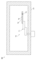
- FIG. 1 is a plan view showing an outline of a configuration of a plasma processing system according to an embodiment of the present invention.
- FIG. 2 is a diagram showing an outline of the configuration of a transport robot provided in a transfer module.
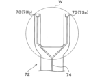
- FIG. 2 is a bottom view showing an outline of the configuration of the fork.
- FIG. 2 is a vertical cross-sectional view showing an outline of the configuration of a processing module.
- FIG. 5 is a partially enlarged view of FIG. 4 .
- FIG. 2 is a partially enlarged cross-sectional view of the electrostatic chuck.
- 1 is a plan view of an example of a jig wafer serving as a jig substrate used to estimate the height of an edge ring; FIG.
- FIG. 13 is a flowchart illustrating an example of a method for estimating the height of an edge ring.
- FIG. 13 illustrates the position of the fork and distance sensor relative to the wafer support pedestal when estimating the edge ring height.
- FIG. 11 is a diagram for explaining another example of the processes of step S3 and step S4.
- FIG. 13 is a plan view illustrating another example of the jig wafer.
- FIG. 11 is a cross-sectional view illustrating another example of the jig wafer.
- FIG. 13 is a diagram showing the results of a test conducted to confirm the repeatability of the edge ring height estimation results using the technology disclosed herein.
- FIG. 11 is a top view for explaining another example of the annular member.
- substrate processing such as etching using plasma, i.e. plasma processing
- plasma processing is performed on substrates such as semiconductor wafers (hereafter referred to as "wafers").
- substrates such as semiconductor wafers (hereafter referred to as "wafers").
- Plasma processing is performed with the substrate placed on a substrate support table inside a reduced pressure processing chamber.
- an edge ring, a cover ring and other annular members in a planar view are placed so as to surround the substrate on the substrate support stand.
- the edge ring also called a focus ring
- the cover ring is an annular member that is placed so as to cover the outer surface of the edge ring.
- a sensor has conventionally been used to estimate the height of an annular member such as an edge ring placed on a substrate support table (in other words, the degree of wear of the annular member).
- the amount of wear of the edge ring may be estimated based on the measured distance from a sensor provided on a transport arm of a substrate transport device that transports substrates to a processing vessel to the surface of the edge ring, and the measured distance from the sensor to the surface of the substrate support table.
- the estimated result may not be accurate.
- the surface of the substrate support table may have intentional irregularities, in which case the estimated result of the height of the annular member will differ depending on which part of the uneven surface that forms the irregularities on the substrate support table surface the sensor is measuring the distance to.
- the irregularities are small, it is difficult to select which part of the uneven surface of the substrate support table surface the sensor is measuring the distance to.
- a dummy substrate such as one made of silicon
- the substrate support stand It is also possible to place a dummy substrate, such as one made of silicon, on the substrate support stand and estimate the height of annular members such as an edge ring based on the distance from the dummy substrate to the sensor.
- a dummy substrate such as one made of silicon
- the adhesive force of the dummy substrate to the substrate support stand will also differ. Therefore, the distance from the dummy substrate to the sensor cannot be measured accurately, and the height of annular members such as an edge ring cannot be accurately estimated.
- the technology disclosed herein accurately estimates the height of the annular member attached to the substrate support stand.
- Fig. 1 is a plan view showing an outline of the configuration of a plasma processing system according to the present embodiment.
- Fig. 2 is a diagram showing an outline of the configuration of a transfer robot provided in a transfer module described later.
- Fig. 3 is a bottom view showing an outline of the configuration of a fork described later.
- substrate processing such as an etching process using plasma, that is, plasma processing.
- the plasma processing system 1 has an atmospheric section 10 that operates under atmospheric pressure and a reduced pressure section 11 that operates under reduced pressure, and these atmospheric section 10 and reduced pressure section 11 are connected together via load lock modules 20, 21.
- the atmospheric section 10 includes an atmospheric module that performs a desired process on the wafer W under atmospheric pressure.
- the reduced pressure section 11 includes a reduced pressure module that performs a desired process on the wafer W under a reduced pressure atmosphere (vacuum atmosphere).
- the load lock modules 20 and 21 are provided to connect the loader module 30 included in the atmospheric section 10 and the transfer module 50 included in the reduced pressure section 11 via a gate valve (not shown).
- the load lock modules 20 and 21 are configured to temporarily hold the wafer W.
- the load lock modules 20 and 21 are also load lock devices configured so that the interior can be switched between an atmospheric pressure atmosphere and a reduced pressure atmosphere.
- the atmospheric section 10 has a loader module 30 as an atmospheric pressure transfer device that operates under atmospheric pressure and has a transfer mechanism 40 described below, and a load port 32 on which a FOUP 31 is placed.
- the FOUP 31 is a storage container capable of storing multiple wafers W.
- the loader module 30 may also be connected to an orienter module (not shown) that adjusts the horizontal orientation of the wafer W, a buffer module (not shown) that temporarily stores multiple wafers W, and the like.
- the loader module 30 has a rectangular housing, and the inside of the housing is maintained at atmospheric pressure.
- a plurality of, for example, five load ports 32 are arranged side by side on one side constituting the long side of the housing of the loader module 30.
- the load lock modules 20 and 21 are arranged side by side on the other side constituting the long side of the housing of the loader module 30.
- a storage module 33 serving as a substrate storage unit for storing a jig wafer Wj serving as a jig substrate is connected to one side surface constituting a short side of the housing of the loader module 30.
- the storage module 33 may also serve as the buffer module described above.
- a transport mechanism 40 configured to hold and transport a wafer W is provided inside the housing of the loader module 30.
- the transport mechanism 40 has a transport arm 41 that supports the wafer W during transport, a rotating table 42 that rotatably supports the transport arm 41, and a base 43 on which the rotating table 42 is mounted.
- a guide rail 44 is provided inside the loader module 30, extending in the longitudinal direction of the loader module 30.
- the base 43 is provided on the guide rail 44, and the transport mechanism 40 is configured to be movable along the guide rail 44.
- the decompression section 11 has a transfer module 50 as a decompression transport device and a processing module 60 as a plasma processing device.
- the decompression section 11 may have a storage module 61 as a material storage section.
- the insides of the transfer module 50 and the processing module 60 (specifically, the insides of the decompression transport chamber 51 and the chamber 100 described below) are each maintained in a decompression atmosphere, and the inside of the storage module 61 is also maintained in a decompression atmosphere.
- multiple processing modules 60 for example six, are provided, and multiple storage modules 61, for example two, are also provided.
- the number and arrangement of the processing modules 60 are not limited to this embodiment and can be set arbitrarily, as long as at least one processing module equipped with a wafer support table described below is provided.
- the number and arrangement of the storage modules 61 are also not limited to this embodiment and can be set arbitrarily, for example at least one is provided.
- the transfer module 50 is configured to transport therein a wafer W.
- the transfer module 50 may also be configured to transport therein an edge ring E, which will be described later.
- the transfer module 50 includes a reduced pressure transfer chamber 51 having a housing having a polygonal shape when viewed from above (a rectangular shape when viewed from above in the illustrated example), and the reduced pressure transfer chamber 51 is connected to the load lock modules 20 and 21 .
- the transfer module 50 transfers the wafer W that has been loaded into the load lock module 20 to one of the processing modules 60 , and also unloads the wafer W that has been subjected to the desired plasma processing in the processing module 60 to the load lock module 21 .
- the transfer module 50 may transport the edge ring E in the storage module 61 to one of the processing modules 60 and may also unload the edge ring E in the processing module 60 to the storage module 61 .
- the processing module 60 performs a desired plasma process, such as an etching process, on the wafer W transferred from the transfer module 50.
- the processing module 60 is also connected to the transfer module 50 via a gate valve 62. The specific configuration of the processing module 60 will be described later.
- the storage module 61 stores the edge ring E.
- the storage module 61 is also connected to the transfer module 50 via a gate valve 63.
- a transfer robot 70 is provided inside the reduced pressure transfer chamber 51 of the transfer module 50.
- the transfer robot 70 is configured to be capable of holding and transferring a wafer W.
- the transfer robot 70 is also configured to be capable of holding and transferring an edge ring E.
- This transport robot 70 has a transport arm 71 that is configured to be able to rotate, extend, and move up and down freely while holding a wafer W.
- the tip of the transport arm 71 is branched into forks 72, 72 that serve as two holding parts.
- the forks 72, 72 are each configured to be able to hold the wafer W and edge ring E to be transported.
- a distance sensor 73 is provided on at least one of the forks 72, 72.
- the distance sensor 73 measures the distance from the fork 72 (specifically, the distance sensor 73) to a target point.
- the fork 72 has a bifurcated shape with a width smaller than the diameter of the wafer W.
- the distance sensor 73 is provided, for example, as a distance sensor 73a at one tip of the bifurcated portion of the fork 72, and a distance sensor 73b at the other tip.
- the distance measurement method using the distance sensor 73 employs a method that allows non-contact measurement in a reduced pressure atmosphere, such as a method based on light.
- the distance sensor 73 irradiates the target with distance measurement light and receives the reflected light, and a unit controller (not shown) connected to the distance sensor 73 via optical fiber 74 measures the distance from the fork 72 (specifically, the distance sensor 73) to the target point based on the light reception result by the distance sensor 73.
- a more specific example of a distance measurement method using the distance sensor 73 is a white light confocal method.
- the white light confocal method for example, white light supplied from a light source (not shown) such as an LED possessed by the unit controller is irradiated from the distance sensor 73 to the object so that the white light is focused at a different height for each wavelength contained in the white light. Then, only the light of the wavelength focused on the object is input to the unit controller via the distance sensor 73 as reflected light. The unit controller calculates the distance from the fork 72 (specifically, the distance sensor 73) to the object point based on the wavelength of the input light.
- the distance sensor 73 is disposed so that the optical axis of the white light is approximately parallel to the vertical direction.
- the white light confocal method is merely one example, and any method capable of measuring distances with a desired accuracy (for example, a vertical resolution of 15 ⁇ m or less and a horizontal resolution of about 0.1 mm) may be used.
- the distance sensor 73 and the unit controller are connected via an optical fiber 74, and the distance measuring light (white light) and reflected light are transmitted via the optical fiber.
- An optical switch (not shown) is interposed in the optical fiber 74.
- the unit controller and the optical switch are provided, for example, in a space outside the reduced pressure transfer chamber 51, which is in an atmospheric environment.
- the unit controller also calculates, i.e. measures, the distance from the fork 72 (specifically the distance sensor 73) to the target point based on the light reception results from the distance sensor 73 as described above, and controls the measurements made by the distance sensor 73 under the control of the control device 80, which will be described later.
- the transfer arm 71 receives the wafer W held in the load lock module 20 and transports it into the processing module 60.
- the transfer arm 71 also receives the wafer W that has been subjected to the desired processing in the processing module 60 and transports it to the load lock module 21.
- the transport arm 71 may receive the edge ring E in the storage module 61 and transport it into the processing module 60.Furthermore, in the transfer module 50, the transport arm 71 may receive the edge ring E in the processing module 60 and transport it out to the storage module 61.
- the plasma processing system 1 includes a controller 80.
- the controller 80 processes computer executable instructions that cause the plasma processing system 1 to perform the various steps described in this disclosure.
- the controller 80 may be configured to control each of the other elements of the plasma processing system 1 such that the plasma processing system 1 performs the various steps described herein.
- some or all of the controller 80 may be included in the other elements of the plasma processing system 1.
- the controller 80 may include, for example, a computer 90.
- the computer 90 may include, for example, a processing unit (CPU: Central Processing Unit) 91, a memory unit 92, and a communication interface 93.
- the processing unit 91 may be configured to perform various control operations and calculations based on programs stored in the memory unit 92.
- the memory unit 92 may include a random access memory (RAM), a read only memory (ROM), a hard disk drive (HDD), a solid state drive (SSD), or a combination thereof.
- the communication interface 93 may communicate with other elements of the plasma processing system 1 via a communication line such as a LAN (Local Area Network).
- LAN Local Area Network
- the transfer mechanism 40 removes the wafer W from the desired FOUP 31 and loads it into the load lock module 20.
- the inside of the load lock module 20 is sealed and depressurized. After that, the inside of the load lock module 20 and the inside of the transfer module 50 are connected to each other.
- the wafer W is then held by the transfer robot 70 and transported from the load lock module 20 to the transfer module 50.
- the gate valve 62 corresponding to the desired processing module 60 is opened, and the transfer robot 70 loads the wafer W into the desired processing module 60.
- the gate valve 62 is then closed, and the desired processing is performed on the wafer W in the processing module 60.
- the processing performed on the wafer W in this processing module 60 will be described later.
- the gate valve 62 is opened, and the wafer W is removed from the processing module 60 by the transfer robot 70. After that, the gate valve 62 is closed.
- the wafer W is loaded into the load lock module 21 by the transfer robot 70.
- the inside of the load lock module 21 is sealed and opened to the atmosphere. After that, the inside of the load lock module 21 and the inside of the loader module 30 are connected to each other.
- the wafer W is held by the transfer mechanism 40 and returned from the load lock module 21 via the loader module 30 to the desired FOUP 31 where it is stored. This completes the wafer processing using the plasma processing system 1.
- the processing module 60 includes a chamber 100 as a processing vessel, a gas supply mechanism 140, an RF (Radio Frequency) power supply unit 150, and an exhaust system 160.
- the processing module 60 also includes a voltage application unit 120 (see FIG. 5).
- the processing module 60 includes a wafer support table 101 as a substrate support table, and an upper electrode 102.
- the chamber 100 is configured so that its interior can be depressurized, and defines a processing space 100s in which plasma is generated.
- the chamber 100 also has a wafer support 101 and other components provided inside.
- the chamber 100 can be made of a material such as aluminum.
- the chamber 100 is also connected to a ground potential.
- the wafer support 101 is disposed, for example, in a lower region within the chamber 100.
- the upper electrode 102 is disposed above the wafer support 101 and can function as part of the ceiling of the chamber 100.
- the wafer support table 101 is configured to support a wafer W.
- the wafer support table 101 includes a lower electrode 103, an electrostatic chuck 104, a support 105, an insulator 106, and a lifter 107.
- the wafer support table 101 may also include a lifter 108.
- the wafer support table 101 is configured to have an edge ring E attached thereto, and more specifically, is configured to also support the edge ring E.
- the wafer support table 101 may or may not include the edge ring E as a component thereof.
- the lower electrode 103 is formed of a conductive material such as aluminum.
- the lower outer periphery of the lower electrode 103 and the upper inner periphery of the support 105 may be formed to overlap in a plan view.
- a flow path 109 for a temperature control fluid is formed inside the lower electrode 103.
- a temperature control fluid is supplied to the flow path 109 from a chiller unit (not shown) provided outside the chamber 100. The temperature control fluid supplied to the flow path 109 is returned to the chiller unit.
- the wafer support table 101 (specifically, the electrostatic chuck 104), the wafer W, or the edge ring E can be cooled to a predetermined temperature by circulating, for example, low-temperature brine as a temperature control fluid in the flow path 109.
- the wafer support table 101 (specifically, the electrostatic chuck 104), the wafer W, or the edge ring E can be heated to a predetermined temperature by circulating, for example, high-temperature brine as a temperature control fluid in the flow path 109.
- the form of the temperature control mechanism is not limited to the above-mentioned flow path 109, and may be another form, such as a resistance heating heater.
- the member on the wafer support table 101 on which the temperature control mechanism is provided is not limited to the lower electrode 103, and may be another member.
- the electrostatic chuck 104 is a member configured to be able to electrostatically attract at least the wafer W, and is provided on the lower electrode 103.
- the electrostatic chuck 104 may also be configured to be able to electrostatically attract the edge ring E.
- the center of the electrostatic chuck 104 constitutes the substrate mounting portion.
- the top surface of the central portion of the electrostatic chuck 104 is higher than the top surface of the peripheral portion.
- the wafer W is mounted on the top surface 104a of the central portion of the electrostatic chuck 104
- the edge ring E is mounted on the top surface 104b of the peripheral portion of the electrostatic chuck 104.
- the top surface 104a of the central portion of the electrostatic chuck 104 becomes a wafer mounting surface as a substrate mounting surface on which the wafer W is mounted
- the top surface 104b of the peripheral portion of the electrostatic chuck 104 becomes a ring mounting surface on which the edge ring E is mounted so as to surround the substrate mounting surface
- the edge ring E is a member arranged to surround the wafer mounting surface, i.e., a member arranged to surround the wafer W, specifically, a member arranged to surround the wafer W mounted on the electrostatic chuck 104.
- the edge ring E is arranged to surround a central portion of the electrostatic chuck 104, the upper surface of which is higher than the peripheral portion.
- the edge ring E is formed in a circular ring shape in a plan view.
- the edge ring E is made of a material such as Si or SiO2 .
- An electrode 110 for electrostatically attracting the wafer W to an upper surface 104a of the central portion is provided in the electrostatic chuck 104.
- An electrode 111 for electrostatically attracting the edge ring E to an upper surface 104b of the peripheral portion may be provided in the electrostatic chuck 104.
- the electrode 111 is, for example, a bipolar type including a pair of electrodes 111a, 111b formed at different positions from each other.
- the electrostatic chuck 104 has a configuration in which electrodes 110 and 111 are sandwiched between insulating materials made of, for example, an insulating material.
- a voltage application unit 120 is connected to the electrode 110 so as to generate an electrical force (specifically, for example, Coulomb force) for electrostatically adsorbing the wafer W.
- an electrical force specifically, for example, Coulomb force
- the voltage application unit 120 includes a DC power supply 121a and a switch 122a.
- the DC power supply 121a is connected to the electrode 110 via the switch 122a, and applies a voltage to the electrode 110 for electrostatically attracting the wafer W.
- the DC power supply 121a can selectively apply a positive voltage or a negative voltage to the electrode 110.
- the voltage application unit 120 may be connected to the electrode 111 so as to generate an electrical force for electrostatically adsorbing the edge ring E. If the electrode 111 is a bipolar type, the voltage application unit 120 may be configured to selectively apply either voltages of opposite polarities or voltages of the same polarity to the pair of electrodes 111a, 111b.
- the voltage application unit 120 includes, for example, two DC power sources 121b and 121c and two switches 122b and 122c.
- the DC power supply 121b is connected to the electrode 111a via, for example, a switch 122b, and selectively applies a positive voltage or a negative voltage for electrostatically attracting the edge ring E to the electrode 111a.
- the DC power supply 121c is connected to the electrode 111b via, for example, a switch 122c, and selectively applies a positive voltage or a negative voltage for electrostatically attracting the edge ring E to the electrode 111b.
- the central portion of the electrostatic chuck 104 where the electrode 110 is provided and the peripheral portion where the electrode 111 is provided are integrated, but these central portion and peripheral portion may be separate.
- the electrode 111 for attracting and holding the edge ring E is a bipolar type, but it may be a unipolar type.
- the upper surface 104a of the central portion of the electrostatic chuck 104 may be provided with a plurality of protrusions 104c. This can reduce the force of adhesion of the wafer W to the electrostatic chuck 104 due to residual charge when the voltage application to the electrode 110 is stopped.
- the plurality of protrusions 104c are provided, for example, at equal intervals.
- the protrusions 104c are formed, for example, in a cylindrical shape with a diameter of 300 ⁇ m to 500 ⁇ m and a height of 5 ⁇ m to 30 ⁇ m.
- the central portion of the electrostatic chuck 104 is formed, for example, with a diameter smaller than the diameter of the wafer W, so that when the wafer W is placed on the upper surface 104 a of the central portion of the electrostatic chuck 104, the peripheral portion of the wafer W protrudes from the central portion of the electrostatic chuck 104.
- the edge ring E has a step formed on its upper portion, and the upper surface of the outer periphery is higher than the upper surface of the inner periphery.
- the inner periphery of the edge ring E is formed to be recessed under the peripheral edge of the wafer W that protrudes from the center of the electrostatic chuck 104. In other words, the inner diameter of the edge ring E is smaller than the outer diameter of the wafer W.
- the support 105 is a member formed in a ring shape in a plan view using an insulating material such as quartz, and is arranged to surround the lower electrode 103 and the electrostatic chuck 104.
- a gas discharge hole may be formed in the central upper surface 104a of the electrostatic chuck 104 to discharge a heat transfer gas into the gap between the rear surface of the placed wafer W and the upper surface 104a.
- a heat transfer gas is supplied from the gas discharge hole from a gas supply unit (not shown).
- the gas supply unit may include one or more gas sources and one or more pressure controllers.
- the gas supply unit is configured to supply the heat transfer gas from the gas source to the gas supply hole via a pressure controller, for example.
- gas discharge holes may be formed on the upper surface 104b of the peripheral portion of the electrostatic chuck 104 to discharge a heat transfer gas into the gap between the back surface of the placed edge ring E and the upper surface 104b.
- the heat transfer gas is supplied from the gas discharge holes from a gas supply unit (not shown).
- the gas supply unit may include one or more gas sources and one or more pressure controllers.
- the gas supply unit is configured to supply the heat transfer gas from the gas source to the gas supply holes via a pressure controller, for example.
- the insulator 106 in FIG. 4 is a cylindrical member made of ceramic or the like, and supports the support 105.
- the insulator 106 is formed, for example, to have an outer diameter equal to the outer diameter of the support 105, and supports the peripheral portion of the support 105.
- the lifter 107 is a member that rises and falls relative to the upper surface 104a at the center of the electrostatic chuck 104, and is formed in a columnar shape, for example, from a ceramic material. When the lifter 107 rises, its upper end protrudes from the upper surface 104a, and the lifter 107 is capable of supporting the wafer W. Three or more lifters 107 are provided at intervals from one another and extend in the vertical direction.
- the lifters 107 are raised and lowered by an actuator 112.
- the actuator 112 has, for example, a support member 113 that supports the multiple lifters 107, and a drive unit 114 that generates a driving force to raise and lower the support member 113 and raise and lower the multiple lifters 107.
- the drive unit 114 has, for example, a motor (not shown) as a driving source that generates the driving force.
- the lifter 107 is inserted into an insertion hole 115 whose upper end opens into the upper surface 104a of the central portion of the electrostatic chuck 104.
- the insertion hole 115 is formed, for example, to extend downward from the upper surface 104a of the central portion of the electrostatic chuck 104 to the bottom surface of the lower electrode 103.
- the above-described lifter 107 enables the transfer of the wafer W between the wafer support table 101 and the transfer arm 71 of the transfer robot 70 .
- the lifter 107 and the actuator 112 form a lifting mechanism that lifts and lowers the wafer W relative to the wafer placement surface.
- the lifter 108 is a lifting member that moves up and down relative to the upper surface 104b of the peripheral portion of the electrostatic chuck 104, and is formed in a columnar shape using, for example, a ceramic material. In one embodiment, the lifter 108 is configured so that its upper end can protrude from the upper surface 105a of the support 105 when raised. Three or more lifters 108 are provided at intervals along the circumferential direction of the electrostatic chuck 104, and extend in the vertical direction.
- the lifter 108 is raised and lowered by an actuator 116.
- the actuator 116 has, for example, a support member 117 provided for each lifter 108, which supports the lifter 108 so that it can move horizontally.
- the support member 117 has, for example, a thrust bearing, to support the lifter 108 so that it can move horizontally.
- the actuator 116 also has a drive unit 118 that generates a driving force to raise and lower the support member 117 and raise and lower the lifter 108.
- the drive unit 118 has, for example, a motor (not shown) as a driving source that generates the driving force.
- the lifter 108 is inserted into an insertion hole 119 whose upper end opens into the upper surface 105a of the support 105.
- the insertion hole 119 is formed, for example, so as to extend downward from the upper surface of the inner periphery of the support 105 to the bottom surface of the lower outer periphery of the lower electrode 103.
- the edge ring E can be transferred between the wafer support table 101 and the transfer arm 71 of the transfer robot 70 by the lifter 108 as described above.
- the lifter 108 and the actuator 116 form another lifting mechanism for raising and lowering the edge ring E relative to the wafer support table 101 .
- the upper electrode 102 also functions as a gas supply or showerhead that delivers one or more gases from the gas supply mechanism 140 into the chamber 100.
- the upper electrode 102 has a gas inlet 102a, a gas diffusion chamber 102b, and a number of gas outlets 102c.
- the gas inlet 102a is, for example, in fluid communication with the gas supply mechanism 140 and the gas diffusion chamber 102b.
- the number of gas outlets 102c are in fluid communication with the gas diffusion chamber 102b and the interior of the chamber 100.
- the upper electrode 102 is configured to deliver a gas, such as one or more process gases, from the gas inlet 102a through the gas diffusion chamber 102b and the number of gas outlets 102c into the chamber 100.
- the gas supply mechanism 140 may include one or more gas sources 141 and one or more flow controllers 142.
- the gas supply mechanism 140 is configured to supply, for example, one or more gases from respective gas sources 141 to the gas inlet 102a via respective flow controllers 142.
- Each flow controller 142 may include, for example, a mass flow controller or a pressure-controlled flow controller.
- the gas supply mechanism 140 may include one or more flow modulation devices to modulate or pulse the flow rate of one or more gases.
- the RF power supply 150 is configured to supply RF power, e.g., one or more RF signals, to one or more electrodes, such as the lower electrode 103, the upper electrode 102, or both the lower electrode 103 and the upper electrode 102. This generates a plasma from one or more process gases supplied in the chamber 100, i.e., the processing space 100s.
- the RF power supply 150 can function as at least a part of a plasma generating unit that generates plasma in the chamber 100.
- the plasma generating unit is specifically configured to generate plasma from one or more gases in the chamber 100.
- the RF power supply 150 includes, for example, two RF generating units 151a, 151b and two matching circuits 152a, 152b.
- the RF power supply 150 is configured to supply a first RF signal from the first RF generating unit 151a to the lower electrode 103 via the first matching circuit 152a.
- the first RF signal may have a frequency in the range of 27 MHz to 100 MHz.
- the RF power supply unit 150 is configured to supply a second RF signal from the second RF generating unit 151b to the lower electrode 103 via the second matching circuit 152b.
- the second RF signal may have a frequency in the range of 400 kHz to 13.56 MHz.
- a DC (Direct Current) pulse generating unit may be used in place of the second RF generating unit 151b.
- one or more RF signals may be pulsed or modulated in amplitude.
- Amplitude modulation may include pulsing the RF signal amplitude between an on state and an off state, or between two or more different on states.
- the exhaust system 160 may be connected to an exhaust port 100e provided at the bottom of the chamber 100, for example.
- the exhaust system 160 may include a pressure valve and a vacuum pump.
- the vacuum pump may include a turbomolecular pump, a roughing pump, or a combination thereof.
- ⁇ Wafer Processing in Processing Module 60 Next, a description will be given of an example of wafer processing performed using the processing module 60.
- a plasma processing such as an etching process is performed on the wafer W.
- the wafer W is loaded into the chamber 100 by the transfer robot 70, and the lifter 107 is raised and lowered to place the wafer W on the electrostatic chuck 104.
- a DC voltage is then applied from the DC power supply 121a to the electrode 110 of the electrostatic chuck 104, so that the wafer W is electrostatically attracted to and held on the electrostatic chuck 104.
- the exhaust system 160 reduces the pressure inside the chamber 100 to a predetermined vacuum level.
- a processing gas is supplied from the gas supply mechanism 140 to the processing space 100s via the upper electrode 102.
- high frequency power HF for plasma generation is supplied from the RF power supply unit 150 to the lower electrode 103, which excites the processing gas and generates plasma.
- high frequency power LF for ion attraction may also be supplied from the RF power supply unit 150. Then, plasma processing is performed on the wafer W by the action of the generated plasma.
- a DC voltage may be applied from DC power sources 121b and 121c to electrode 111 of electrostatic chuck 104, thereby electrostatically attracting and holding edge ring E on electrostatic chuck 104.
- a heat transfer gas may be ejected toward the bottom surfaces of wafer W and edge ring E attracted and held on electrostatic chuck 104.
- the supply of high frequency power HF from the RF power supply unit 150 and the supply of processing gas from the gas supply mechanism 140 are stopped. If high frequency power LF was being supplied during plasma processing, the supply of the high frequency power LF is also stopped. Next, the adsorption and holding of the wafer W by the electrostatic chuck 104 is stopped. In addition, the supply of heat transfer gas to the bottom surface of the wafer W may be stopped.
- the wafer W is raised by the lifter 107 and detached from the electrostatic chuck 104.
- a de-electrification process may be performed on the wafer W.
- the transfer robot 70 removes the wafer W from the chamber 100, completing the series of wafer processing steps.
- waferless dry cleaning may be performed after the wafer W is unloaded from the chamber 100. That is, after the wafer W is unloaded from the chamber 100, plasma may be generated in the chamber 100 and the electrostatic chuck 104 may be cleaned by the plasma in a state in which the wafer W is not placed on the wafer mounting surface of the electrostatic chuck 104. Specifically, after the wafer W is unloaded, a cleaning gas may be supplied from the gas supply mechanism 140 to the processing space 100s via the upper electrode 102 in a state where the wafer W is not placed on the central upper surface 104a of the electrostatic chuck 104, which is the wafer placement surface.
- a high frequency power HF for plasma generation may be supplied from the RF power supply unit 150 to the lower electrode 103, for example, so that the gas is excited to generate plasma.
- the generated plasma can remove reaction products attached to, for example, a portion between the central portion of the electrostatic chuck 104 and the edge ring E.
- the high frequency power HF for generating plasma may be supplied to the upper electrode 102 .
- Fig. 7 is a plan view of an example of a jig wafer as a jig substrate used for estimating the height of the edge ring E.
- Fig. 8 is a flowchart showing an example of a method for estimating the height of the edge ring E.
- Fig. 9 is a diagram showing the positions of the fork 72 and the distance sensor 73 relative to the wafer support table 101 when estimating the height of the edge ring E. Note that in each of the following steps, the exhaust system 160 continuously evacuates the chamber 100.
- the edge ring E placed on the electrostatic chuck 104 is worn down by the aforementioned wafer processing using plasma.
- the degree of wear of the edge ring E can be determined from the height of the edge ring E placed on the electrostatic chuck 104. Therefore, in the plasma processing system 1, the control device 80 estimates the height of the edge ring E placed on the electrostatic chuck 104.
- a jig wafer Wj as exemplified in FIG. 7 is used.
- the jig wafer Wj has the same shape and material in a plan view as the wafer W on which the plasma processing is actually performed.
- the jig wafer Wj and the wafer W are made of silicon, for example.
- the jig wafer Wj has a reference surface Ws that serves as a reference for the height of the edge ring E, and is placed on the electrostatic chuck 104 so that the reference surface Ws is on the upper side.
- the surface of the jig wafer Wj that is on the upper side when placed on the electrostatic chuck 104 is referred to as the upper surface.
- the entire upper surface of the jig wafer Wj is formed flat, and the entire upper surface serves as a reference surface Ws.
- the thickness of the jig wafer Wj may be the same as or different from that of the actual wafer W.
- the jig wafer Wj is stored, for example, in a storage module 33 when not in use.
- Step S1 In the plasma processing system 1, when estimating the height of the edge ring E, for example, first, as shown in FIG. 8, under the control of the control device 80, the jig wafer Wj is transported into the chamber 100 by the transport robot 70, and placed on the wafer support table 101 by the lifting mechanism.
- the jig wafer Wj in the storage module 33 is transferred by the transfer mechanism 40 and the transfer robot 70 into the chamber 100 of the processing module 60 to which the edge ring E, the height of which is to be measured, is attached (hereinafter, the processing module 60 to be measured).
- the jig wafer Wj is transferred from the transfer robot 70 to the lifter 107 .
- the lifter 107 is raised, and the jig wafer Wj is transferred from the transfer arm 71 to the lifter 107.
- the transfer arm 71 is removed from the chamber 100, and the gate valve 62 is closed.
- the jig wafer Wj is lowered by a lifting mechanism including a lifter 107 and placed on the upper surface 104a (hereinafter, wafer placement surface 104a) at the center of the electrostatic chuck 104. Specifically, the lifter 107 is lowered until the upper end of the lifter 107 fits into the insertion hole 115. As a result, the jig wafer Wj is placed on the wafer placement surface 104a.
- Step S2 Next, under the control of the control device 80, a predetermined voltage is applied to the electrostatic chuck 104 while a predetermined gas is supplied into the chamber 100, and the jig wafer Wj is electrostatically attracted to the wafer mounting surface 104a in a plasma-free manner. Specifically, for example, the following steps S2a to S2c are performed.
- Step S2a In this process, first, a gas for increasing the charge amount is supplied into the chamber 100 .
- an inert gas such as nitrogen gas or argon gas
- oxygen gas is supplied as a charge increasing gas from the gas supply mechanism 140 into the chamber 100 via the upper electrode 102 .
- the pressure in the chamber 100 may be controlled to be 100 mTorr or more. However, if a charge increasing gas is supplied into the chamber 100, the pressure in the chamber 100 does not need to be controlled.
- Step S2b After step S2a, a predetermined voltage is applied to the electrostatic chuck 104, and the fixture wafer Wj is electrostatically attracted to the wafer mounting surface 104a in a plasma-less manner. Specifically, in a state where the supply of the charge increasing gas is continued and the RF power supply unit 150 does not supply the high frequency power HF for generating plasma, a voltage of 1500V to 6000V is applied from the DC power supply 121a to the electrode 110 of the electrostatic chuck 104. As a result, the jig wafer Wj is electrostatically attracted to the central upper surface 104a of the electrostatic chuck 104, which is the wafer mounting surface, without plasma.
- the charge increasing gas is supplied at this time, an event occurs which is electrically equivalent to the transfer of charge from the chamber 100 connected to the ground potential to the jig wafer Wj via the charge increasing gas. Therefore, the charge of the jig wafer Wj increases compared to the case where the charge increasing gas is not supplied, and the electrostatic adsorption force of the jig wafer Wj to the wafer mounting surface 104a becomes stronger.
- Step S2c After step S2b, the supply of the predetermined gas is stopped. Specifically, while the electrostatic attraction of the fixture wafer Wj continues, the supply of the charge increasing gas from the gas supply mechanism 140 to the chamber 100 via the upper electrode 102 is stopped.
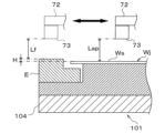
- Step S3 Then, under the control of the control device 80, the fork 72 of the transport robot 70 is positioned above the wafer support table 101, and the distance sensor 73 measures the distance to the reference surface Ws of the jig wafer Wj placed on the wafer mounting surface 104a and the distance to the edge ring E attached to the wafer support table 101.
- the gate valve 62 is opened, and the fork 72 is moved above the wafer support table 101 on which the jig wafer Wj and the edge ring E are placed, as shown in FIG. 9. Furthermore, while the electrostatic attraction of the jig wafer Wj is continued, the distance from the fork 72 (specifically, the distance sensor 73) located above the wafer support table 101 to the reference surface Ws of the jig wafer Wj and the distance from the fork 72 (specifically, the distance sensor 73) to the edge ring E are measured by the distance sensor 73.
- light for distance measurement is irradiated from the distance sensor 73 to a predetermined reference position on the reference surface Ws of the jig wafer Wj, and the reflected light is received by the distance sensor 73.
- the reference position is provided, for example, at the peripheral end of the jig wafer Wj.
- the distance Lsp from the fork 72 to the predetermined reference position on the reference surface Ws of the jig wafer Wj is calculated by the unit controller described above.
- light for distance measurement is irradiated from the distance sensor 73 to a predetermined measurement position on the edge ring E, and the reflected light is received by the distance sensor 73.
- the measurement position is provided, for example, at the inner peripheral end of the edge ring E, that is, the peripheral end of the edge ring E on the jig wafer W side.
- the unit controller calculates the distance Lf from the fork 72 to the edge ring E.
- “the distance from the fork 72 to XX” may be abbreviated to "the distance to XX”.
- the fork 72 is removed from the chamber 100 and the gate valve 62 is closed.
- Step S4 the control device 80 calculates, i.e., estimates, the height of the edge ring E based on the distance to the reference surface Ws and the distance to the edge ring E.
- the control device 80 calculates the height H of the edge ring E (specifically, the height from the reference surface Ws) based on the following formula (X) using the above-mentioned distance Lsp and the above-mentioned distance Lf.
- H Lsp-Lf...(X)
- Step S5 Thereafter, under the control of the control device 80, the application of a predetermined voltage to the electrostatic chuck 104, which is used for electrostatic attraction of the fixture wafer Wj, is stopped. Specifically, the application of voltage from the DC power supply 121a to the electrode 110 of the electrostatic chuck 104 is stopped.
- Step S6 Subsequently, a static elimination gas is supplied into the chamber 100, and the jig wafer Wj placed on the wafer placement surface 104a is neutralized without using plasma. Specifically, for example, the following steps S6a to S6d are performed.
- Step S6a In this process, first, a static elimination gas is supplied into the chamber 100 . Specifically, an inert gas (such as nitrogen gas or argon gas) or oxygen gas is supplied as a static elimination gas from the gas supply mechanism 140 into the chamber 100 via the upper electrode 102.
- the static elimination gas may be the same as or different from the charge increasing gas.
- the pressure inside the chamber 100 may be controlled to be 700 mTorr ⁇ 100 mTorr.
- Step S6b After step S6a, a voltage of a predetermined magnitude and of polarity opposite to that of step S2b is applied to the electrostatic chuck 104, and the fixture wafer Wj placed on the wafer placement surface 104a is neutralized in a plasma-less manner. Specifically, in a state where the supply of the static elimination gas into the chamber 100 is continued and in a state where the high frequency power HF for generating plasma is not supplied from the RF power supply unit 150, a voltage of 100 V to 1500 V with a polarity opposite to that in step S2b is applied from the DC power supply 121a to the electrode 110 of the electrostatic chuck 104.
- the application of such a voltage of the opposite polarity causes an event that is electrically equivalent to the electric charge of the fixture wafer Wj before the application of the voltage flowing through the gas in the chamber 100 to the ground potential to which the chamber 100 is connected, and the occurrence of the event is accelerated, so that the fixture wafer Wj can be neutralized without plasma.
- the application time of the reverse polarity voltage is, for example, 5 seconds, and when this application time is exceeded, the application is stopped.
- Step S6c After step S6b, with no voltage being applied to the electrostatic chuck 104, a static electricity removing gas is supplied into the chamber 100, and the jig wafer Wj placed on the wafer placement surface 104a is further destaticized. Specifically, following steps S6a and S6b, the supply of the static elimination gas into the chamber 100 continues for a predetermined time with no voltage being applied to the electrostatic chuck 104. This causes an event that is electrically equivalent to the flow of the charge on the fixture wafer Wj to the ground potential to which the chamber 100 is connected via the static elimination gas in the chamber 100, so that the fixture wafer Wj can be further neutralized without plasma.
- step S6b The supply time of the static elimination gas in this step S6b is, for example, 30 to 60 seconds.
- step S6c the pressure inside the chamber 100 may be controlled in the same manner as in step S6a. Incidentally, this step S6c may be omitted.
- Step S6d After step S6c, the supply of the static elimination gas is stopped. Specifically, the supply of the static elimination gas from the gas supply mechanism 140 to the chamber 100 via the upper electrode 102 is stopped.
- Step S7 Then, under the control of the controller 80 , the jig wafer Wj is separated from the wafer support table 101 by the lifting mechanism, and is carried out of the chamber 100 by the transfer robot 70 .
- the jig wafer Wj is raised by a lifting mechanism including a lifter 107 and separated from the wafer placement surface 104a. More specifically, the lifter 107 is raised until the upper end of the lifter 107 protrudes from the wafer mounting surface 104a, and the jig wafer Wj is separated from the wafer mounting surface 104a. After the separation, the jig wafer Wj is raised to a predetermined height by the lifting of the lifter 107.
- the jig wafer Wj is transferred from the lifter 107 to the transfer robot 70 .
- the gate valve 62 is opened, and the transfer arm 71 of the transfer robot 70 is inserted into the chamber 100.
- the transfer arm 71 is moved between the jig wafer Wj supported by the lifter 107 and the electrostatic chuck 104.
- the lifter 107 is lowered, and the jig wafer Wj is transferred to the transfer arm 71.
- the jig wafer Wj in the chamber 100 is returned to the storage module 33 by the transfer robot 70 and the transfer mechanism 40 .
- the transfer arm 71 is removed from the chamber 100, and the jig wafer Wj is transferred from the chamber 100 to the transfer module 50.
- the gate valve 62 is closed.
- the interior of the transfer module 50 is connected to the interior of the depressurized load lock module 20.
- the jig wafer Wj is transferred into the load lock module 20.
- the inside of the load lock module 20 is sealed and returned to atmospheric pressure.
- the jig wafer Wj in the load lock module 20 is held by the transfer arm 41 of the transfer mechanism 40, and is returned to the storage module 33.
- the plasma processing system 1 estimates the height of the edge ring E placed on the electrostatic chuck 104, for example, every time a predetermined time elapses or every time a predetermined number of wafers W are processed.
- the height of the edge ring E can be accurately estimated.
- the measurement result of the distance to the reference plane Ws is used to estimate the distance to the edge ring E, even if the fork 72 sags under its own weight due to aging or the like, the height of the edge ring E can be accurately estimated.
- a predetermined voltage is applied to the electrostatic chuck 104 while a charge-increasing gas is supplied into the chamber 100, and the jig wafer Wj is electrostatically attracted to the wafer mounting surface 104a. Therefore, the charge of the jig wafer Wj when electrostatically attracted to the wafer mounting surface 104a can be increased compared to the case where a charge-increasing gas is not supplied into the chamber 100 when the above-mentioned predetermined voltage is applied to the electrostatic chuck 104. This point will be explained below.
- the wafer mounting surface 104a may be charged before the jig wafer Wj is placed on it.
- the amount of charge on the wafer mounting surface 104a before the jig wafer Wj is placed on it may vary depending on whether the above-mentioned waferless cleaning is performed and the contents of the waferless cleaning. If the amount of charge varies, the electrostatic adsorption force of the jig wafer Wj to the wafer mounting surface 104a also varies. The strength of this electrostatic adsorption force affects the height of the reference surface Ws of the jig wafer Wj electrostatically adsorbed to the wafer mounting surface 104a.
- the amount of charge of the jig wafer Wj can be increased when electrostatically adsorbed to the wafer mounting surface 104a as described above, it is possible to suppress the influence of the difference in the amount of charge of the wafer mounting surface 104a before placing the jig wafer Wj on the electrostatic adsorption force of the jig wafer Wj to the wafer mounting surface 104a. Therefore, it is possible to suppress the influence of the difference in the amount of charge of the wafer mounting surface 104a before placing the jig wafer Wj on the height of the reference surface Ws when measuring the distance to the reference surface Ws of the jig wafer Wj. Therefore, it is possible to suppress the influence of the difference in the amount of charge of the wafer mounting surface 104a before placing the jig wafer Wj on the estimated result of the height of the edge ring E.
- the process of increasing the amount of charge on the jig wafer Wj on the wafer mounting surface 104a in step S2 is performed without plasma. Therefore, the reference surface Ws of the jig wafer Wj is not damaged by plasma due to the process of increasing the amount of charge on the jig wafer Wj. Therefore, it is possible to prevent the accuracy of the estimation result of the height of the edge ring E based on the measurement result of the height of the reference surface Ws from being impaired by the process of increasing the amount of charge on the jig wafer Wj.
- a voltage of the opposite polarity to that at the time of adsorption of the jig wafer Wj to the electrostatic chuck 104 is applied to the electrostatic chuck 104, and the jig wafer Wj on the wafer mounting surface 104a is neutralized. Therefore, even if the electrostatic attraction force of the jig wafer Wj to the wafer mounting surface 104a is high due to the process of increasing the charge amount of the jig wafer Wj as described above, the electrostatic attraction force is weakened by the charge removal.
- the jig wafer Wj electrostatically attracted to the wafer mounting surface 104a from becoming unable to be removed from the wafer mounting surface 104a.
- the jig wafer Wj can be used stably when estimating the height of the edge ring E.
- the magnitude of the reverse polarity voltage applied to the electrostatic chuck 104 during neutralization is 100 V to 1500 V.
- the voltage By setting the voltage to 100 V or more, it is possible to more reliably prevent the fixture wafer Wj from becoming unable to be removed from the wafer mounting surface 104a.
- the voltage By setting the voltage to 1500 V or less, it is possible to prevent the fixture wafer Wj from becoming charged with a polarity opposite to that before neutralization began, making it impossible to remove the fixture wafer Wj from the wafer mounting surface 104a.
- the static elimination process of the jig wafer Wj is performed without plasma. Therefore, the static elimination process of the jig wafer Wj does not cause damage to the reference surface Ws of the jig wafer Wj, which is used repeatedly, by plasma. Therefore, it is possible to prevent the accuracy of the estimation result of the height of the edge ring E, which is based on the measurement result of the height of the reference surface Ws, from being impaired by the static elimination process of the jig wafer Wj.
- a neutralization gas is supplied into the chamber 100 in a state where no voltage is applied to the electrostatic chuck 104, and the jig wafer Wj mounted on the wafer mounting surface 104a is neutralized without plasma.
- the inventors have conducted tests employing the method of separating the jig wafer Wj from the wafer mounting surface 104a according to the present disclosure, and have confirmed the following: That is, according to this separating method, even if the voltage applied to the electrostatic chuck 104 for electrostatically attracting the jig wafer Wj is as high as 3000 V, the jig wafer Wj can be removed from the wafer support table 101 without damaging the jig wafer Wj, etc., and the jig wafer Wj does not move significantly in the horizontal direction during separation. In addition, it has been confirmed that these points are not dependent on the temperature of the chamber 100.
- the control device 80 estimates the height of the edge ring E based on the measurement results of the distance to a predetermined reference position on the reference surface Ws of the jig wafer Wj on the wafer mounting surface 104a and the distance to a predetermined measurement position of the edge ring E, measured by the distance sensor 73 provided on the fork 72 of the transport robot 70.
- the reference position is provided on the peripheral edge of the jig wafer Wj
- the measurement position is the peripheral edge of the edge ring E on the jig wafer Wj side, and the reference position and the measurement position are close to each other. Therefore, even if sagging occurs depending on the penetration distance of the fork 72 into the chamber 100, the measurement error caused by the sagging can be suppressed, and the height of the edge ring E can be more accurately estimated.
- Figure 10 is a diagram for explaining another example of the process in which the height of the reference surface Ws of the jig wafer Wj and the height of the edge ring E are measured in step S3, and the process in which the control device 80 estimates the height of the edge ring E in step S4.
- the fork 72 When measuring the distance to the edge ring E in step S3, the fork 72 may be moved under the control of the control device 80 so that the distance sensor 73a moves in a predetermined direction, as shown in FIG. 10.
- the above-mentioned predetermined direction is a direction that crosses the edge ring E in a plan view and intersects with the direction in which the fork 72 is inserted and removed from the chamber 100 (the up-down direction in FIG. 10).
- the method of moving the distance sensor 73a in a direction across the edge ring E in a plan view may be to rotate the fork 72 around the base end of the fork 72 on which the distance sensor 73a is provided, or to rotate the transport arm 71 around the base end of the transport arm 71.
- the distance Lf to the edge ring E may be continuously measured by the distance sensor 73a. Then, in step S4, the control device 80 may estimate the distribution of the height of the edge ring E in the crossing direction, i.e., the profile, based on the results of continuous measurements of the distance Lsp to the reference point of the reference surface Ws of the jig wafer Wj and the distance Lf to the edge ring E.
- control device 80 may calculate the height H of the edge ring E for each measurement point of the distance Lf to the edge ring E based on the above formula (X), and create the distribution of the height of the edge ring E in the crossing direction from each calculation result and the position information of each measurement point.
- the position information of each measurement point can be calculated from the angle and size of each component of the transfer arm 71 when the distance Lf is measured.
- the control device 80 may estimate the height of the edge ring E based on the average value of continuous measurement results of the distance Lsp to the reference point of the reference surface Ws of the jig wafer Wj and the distance Lf to the edge ring E.
- step S3 and step S4 when the fork 72 is moved so that the distance sensor 73a moves in the crossing direction as in the above-mentioned alternative example 1, the fork 72 may vibrate during the movement.
- the fork 72 vibrates if the height profile of the edge ring E is estimated as in other example 1 described above, the profile may be the actual profile of the height of the edge ring E with the vibration component of the fork 72 superimposed thereon.
- step S3 as shown in FIG. 10, while the fork 72 is moved so that one distance sensor 73a moves in a direction crossing the edge ring E in a plan view, the distance to the edge ring E may be continuously measured by the one distance sensor 73a.
- the other distance sensor 73b may continuously measure the distance to the reference surface Ws of the jig wafer Wj.
- the control device 80 may create a height profile in the above-mentioned crossing direction of the edge ring E from the calculation results of the above-mentioned height Ht for each point in time during measurement by the distance sensors 73a and 73b and the position information of the measurement point by the distance sensor 73a.
- the profile thus obtained is one in which the influence of the vibration component D2 of the fork 72 has been removed. Moreover, the profile thus obtained is free of the effect of the inclination of the fork 72 relative to the wafer support table 101 .
- step S3 (Another example 3 of step S3 and step S4)
- the fork 72 may be moved not only in a plan view by the distance sensor 73a moving leftward to cross the edge ring E, but also in a plan view by the distance sensor 73b moving rightward to cross the edge ring E.
- “left” and “right” are based on the loading/unloading port of the chamber 100.
- the distance sensor 73a may measure the distance Lsp to a reference point on the left side of the reference surface of the jig wafer Wj, and the distance sensor 73a may continuously measure the distance Lf to the edge ring E on the left side of the edge ring E.
- the distance sensor 73b may measure the distance to a reference point on the right side of the reference surface of the jig wafer Wj, and the distance sensor 73a may continuously measure the distance Lf to the edge ring E on the right side of the edge ring E.
- the control device 80 may estimate a height profile in the transverse direction on the left side of the edge ring E, for example, based on continuous measurement results of the distance Lsp to a reference point on the left side of the reference surface of the jig wafer Wj and the distance Lf to the edge ring E on the left side of the edge ring E.
- the control device 80 may estimate a height profile in the transverse direction on the right side of the edge ring E, for example, based on continuous measurement results of the distance Lsp to a reference point on the right side of the reference surface of the jig wafer Wj and the distance Lf to the edge ring E on the right side of the edge ring E.
- the control device 80 may average the height estimation results of corresponding positions in the height profile on the left side of the edge ring E and the height profile on the right side of the edge ring E to generate a representative height profile of the edge ring E.
- step S4 the control device 80 may estimate the height of the left side of the edge ring E based on the average value of the results of continuous measurements of the distance Lsp to the reference point on the left side of the reference surface of the jig wafer Wj and the distance Lf to the edge ring E on the left side of the edge ring E.
- step S4 the control device 80 may estimate the height of the right side of the edge ring E based on the average value of the results of continuous measurements of the distance Lsp to the reference point on the right side of the reference surface of the jig wafer Wj and the distance Lf to the edge ring E on the right side of the edge ring E.
- the control device 80 may calculate the average value of the height of the left side of the edge ring E and the height of the right side of the edge ring E, and use the calculated result as the representative height of the edge ring E.
- step S4 the control device 80 may correct the estimated result of the height of the edge ring E based on the distance Lsp to the reference point on the reference surface Ws of the jig wafer Wj measured by the distance sensor 73 and the design value of the distance Lsp. In this way, when the fork 72 sags under its own weight due to aging or the like, the influence of the sagging can be removed from the estimated result of the height of the edge ring E.
- the design value of the distance Lsp is stored in advance in a storage unit (not shown).
- FIG. 11 and 12 are a plan view and a cross-sectional view, respectively, that show a schematic diagram of another example of a jig wafer.
- the jig wafer WjA has a plurality of correction surfaces Wr spaced a predetermined distance in the height direction from the reference surface Ws, and the plurality of correction surfaces Wr have different distances from the reference surface Ws in the height direction.
- correction surfaces Wr1 to Wr3 are provided as the correction surface Wr for each of the distance sensor 73a and the distance sensor 73b. The distances of the correction surfaces Wr1 to Wr3 from the reference plane Ws are determined with high precision in advance.
- the jig wafer WjA has a member WJA1 having step surfaces of different heights provided on the reference plane Ws, and each step surface constitutes the correction surfaces Wr1 to Wr3.
- the jig wafer WjA may have grooves formed with different recess depths from the reference plane Ws, and the bottom surfaces of the grooves may constitute the correction surfaces Wr1 to Wr3.
- the distances of the correction surfaces Wr1, Wr2, and Wr3 from the reference surface Ws are, for example, 100 ⁇ m, 50 ⁇ m, and 25 ⁇ m, respectively.
- the member WJA1 of the jig wafer WjA is, for example, made of the same material as the wafer W to be plasma processed, and is used by being adhered to the reference surface Ws.
- the distance sensor 73 also measures the distances to the multiple correction surfaces Wr when it measures the distance to the reference surface Ws and the distance to the edge ring E. For example, the distance sensor 73 measures the distance to the correction surface Wr1 and the distance to the correction surface Wr2. The control device 80 then corrects the measurement results by the distance sensor 73 based on the measurement results of the distances to the multiple correction surfaces Wr. Specifically, the control device 80 obtains, for example, a difference Df between the distance to the correction surface Wr1 and the distance to the correction surface Wr2 measured by the distance sensor 73.
- the control device 80 then corrects the measurement results by the distance sensor 73 so that this difference Df approaches a design value of the difference Df. This allows the control device 80 to obtain more accurate distances to the reference surface Ws and the edge ring E, and as a result, to more accurately estimate the height of the edge ring E.
- the design value of the difference Df is stored in advance in a storage unit (not shown).
- the correction surface Wr is provided in the following area of the jig wafer WjA. That is, the correction surface Wr is provided in an area on the jig wafer WjA where continuous measurement of the distance to the reference surface Ws by the distance sensors 73a and 73b is not impeded when the fork 72 is moved.
- FIG. 13 is a diagram showing the results of a test performed to confirm the repeatability of the estimation result of the height of the edge ring E by the technique according to the present disclosure.
- the height of the edge ring E was estimated by the method including the above-mentioned steps S1 to S7 at different timings between the plasma processing.
- the timings at which the height of the edge ring E was estimated were when the total time of the plasma processing performed on the wafer W in the corresponding processing module 60 was Z1 to Z7 (Z1 to Z7 are different times from 0 hours to 500 hours).
- the horizontal axis indicates the radial position of the edge ring E
- the vertical axis indicates the repeatability of the estimation result of the height of the edge ring E at each estimation timing, specifically, the difference between the maximum value and the minimum value of the estimated height of the edge ring E at each estimation timing. Note that one scale on the vertical axis corresponds to 0.005 m.
- the difference between the maximum and minimum values of the estimated height of the edge ring E was equal to or less than the target value regardless of the estimation timing or the radial position of the edge ring E.
- the height of the edge ring E that is consumed by plasma can be estimated with high accuracy over a long period of time without changing the jig wafer Wj.
- One of the correction surfaces Wr of the jig wafer WjA may be used as a reference surface Ws for the height of the edge ring E.
- the amount of wear of the edge ring E can be determined from the estimated result of the height of the edge ring E. Therefore, when the amount of wear of the edge ring E exceeds a threshold, that is, when the height of the edge ring E falls below the threshold, the edge ring E may be replaced, or a voltage may be applied to the edge ring E to change the shape of the sheath on the edge ring E side.
- the chamber 100 When replacing the edge ring E, under the control of the control device 80, the chamber 100 is not opened to the atmosphere, and the edge ring E whose estimated height is below the threshold is separated from the wafer support table 101 by a lifting mechanism including a lifter 108, and is removed from the chamber 100 by the transfer robot 70.
- the edge ring E is raised by a lifting mechanism including a lifter 107 and separated from the upper surface (hereinafter, ring mounting surface) 104 b of the peripheral portion of the electrostatic chuck 104 . More specifically, the lifter 108 is raised until the upper end of the lifter 108 protrudes from the ring mounting surface 104b, thereby separating the edge ring E from the ring mounting surface 104b. After the edge ring E is separated from the ring mounting surface 104b, the edge ring E is raised to a predetermined height by the raising of the lifter 108.
- the edge ring E is transferred from the lifter 108 to the transfer robot 70 .
- the gate valve 62 is opened, and the transfer arm 71 of the transfer robot 70 is inserted into the chamber 100.
- the transfer arm 71 is moved between the edge ring E supported by the lifter 108 and the electrostatic chuck 104.
- the lifter 108 is lowered, and the edge ring E is transferred to the transfer arm 71.
- the edge ring E in the chamber 100 is transferred to the storage module 61 by the transfer robot 70 .
- the transfer arm 71 is extracted from the chamber 100, and the edge ring E is transferred from the chamber 100 to the transfer module 50.
- the gate valve 62 is closed, and the gate valve 63 is opened.
- the edge ring E is stored in the storage module 61.
- the replacement edge ring E is transported into the chamber 100 by the transport robot 70 and placed on the wafer support table 101 by the lifting mechanism including the lifter 180.
- the replacement edge ring E in the storage module 61 is held by the transfer arm 71 of the transfer robot 70.
- the transfer arm 71 holding the edge ring E is inserted into the corresponding chamber 100 through a loading/unloading port (not shown).
- the edge ring E is transferred by the transfer arm 71 above the ring mounting surface 104b.
- the edge ring E is transferred from the transfer robot 70 to the lifter 108 .
- the lifter 108 is raised, and the edge ring E is transferred from the transfer arm 71 to the lifter 108.
- the transfer arm 71 is removed from the chamber 100, and the gate valve 62 is closed.
- the edge ring E is lowered by the lifting mechanism including the lifter 107 and placed on the ring placement surface 104b. Specifically, the lifter 108 is lowered until the upper end of the lifter 108 fits into the insertion hole 119. As a result, the edge ring E is placed on the ring placement surface 104b.
- the replacement edge ring E may be a new one, or may be a used one with only a small amount of wear.
- the jig wafer Wj was stored in the storage module 33, but it may also be stored in the FOUP 31 or the storage module 61.
- the storage module 61 serving as a material storage section for storing the edge ring E was connected to the transfer module 50, but the material storage section may be connected to one side constituting the long side or one side constituting the short side of the housing of the loader module 30.
- the FOUP 31 placed on the load port 32 may be the material storage section.
- the transport mechanism 40 may be configured to be able to transport the edge ring E for replacement.
- a cover ring C may be attached to the wafer support stand as an annular member, which is arranged to cover the outer surface of the edge ring E, as shown in FIG. 14.
- the technology disclosed herein can also be applied to estimating the height of the cover ring C attached to the wafer support stand.
- a plasma processing system comprising: A plasma processing apparatus, a reduced pressure transport apparatus having a transport robot connected to the plasma processing apparatus and transporting a substrate, and a control apparatus
- the plasma processing apparatus includes: A processing container configured to be decompressible; a substrate support provided in the processing chamber, the substrate support having a substrate mounting surface and an electrostatic chuck configured to electrostatically attract a substrate to the substrate mounting surface, the substrate support having an annular member attached to the substrate mounting surface so as to surround the substrate mounting surface; a lifting mechanism for lifting and lowering a substrate relative to the substrate placement surface; a gas supply unit that supplies a gas into the processing chamber;
- the transport robot includes: a holder configured to hold a substrate to be transported; a distance sensor provided in the holding portion and measuring a distance from the holding portion;
- the control device includes: (A) carrying a jig substrate having a reference surface that is a reference for the height of the annular member into the processing chamber by the transfer robot,
- step (E) The control device (E) supplying the gas into the processing vessel and removing electricity from the jig substrate placed on the substrate placement surface in a plasma-less manner; (F) after the step (E), a step of separating the jig substrate from the substrate support table by the lifting mechanism and removing the jig substrate from the processing chamber by the transfer robot is further performed;
- step (E) includes the step of: (H) supplying the gas into the processing vessel while no voltage is applied to the electrostatic chuck, thereby removing electricity from the fixture substrate placed on the substrate mounting surface in a plasma-less manner.
- step (H) is performed after the step (G).
- the gas is an inert gas or an oxygen gas.
- the plasma processing apparatus further includes another lifting mechanism for raising and lowering the annular member relative to the substrate support table,
- the transport robot is configured to also transport the annular member,
- the control device includes: (I) when the height of the annular member estimated in the step (D) is below a threshold value, moving the annular member away from the substrate support table by the separate lifting mechanism and removing the annular member from the processing chamber by the transfer robot; (J) after step (I), a step of loading a replacement annular member into the processing vessel by the transport robot and placing it on the substrate support table by the separate lifting mechanism is further executed.
- a member storage section for storing the annular member
- an atmospheric pressure transfer device connected to the reduced pressure transfer device via a load lock device configured to switch the inside between an atmospheric pressure atmosphere and a reduced pressure atmosphere, and having a transfer mechanism that operates under atmospheric pressure and transfers a substrate;
- An atmospheric section is further provided which is connected to the reduced pressure transport apparatus via a load lock device configured to switch the inside between an atmospheric pressure atmosphere and a reduced pressure atmosphere and which operates under an atmospheric pressure atmosphere;
- the jig substrate is The substrate is stored in a storage container that is placed in the atmospheric section and configured to be able to store a plurality of substrates, or
- the annular member is an edge ring arranged adjacent to the substrate on the substrate support table, or a cover ring arranged to cover the outer surface of the edge ring.
- the (C) step includes moving the holding part above the substrate support table so that the distance sensor crosses the annular member in a plan view, and using the distance sensor to measure the distance to the reference surface of the jig substrate placed on the substrate placement surface and continuously measuring the distance to the annular member attached to the substrate support table;
- a method for estimating a height of an annular component in a plasma processing system comprising: The plasma processing system includes: a plasma processing apparatus; and a reduced pressure transfer apparatus having a transfer robot connected to the plasma processing apparatus and transferring a substrate,
- the plasma processing apparatus includes: A processing container configured to be decompressible; a substrate support provided within the processing chamber, the substrate support having a substrate mounting surface and an electrostatic chuck configured to electrostatically attract a substrate to the substrate mounting surface, the substrate support having the annular member attached thereto so as to surround the substrate mounting surface; a lifting mechanism for lifting and lowering the substrate relative to the substrate placement surface
- the transport robot includes: a holder configured to hold a substrate to be transported; a distance sensor provided in the holding portion and measuring a distance from the holding portion; (A) carrying a jig substrate having a reference surface that is a reference for the height of the annular member into the processing chamber by the transfer robot, and placing the jig substrate on the substrate support table by the lifting mechanism; (B)
- Plasma processing system 50 Transfer module 60 Processing module 70 Transfer robot 72 Forks 73, 73a, 73b Distance sensor 80 Control device 100 Chamber 101 Wafer support table 102 Upper electrode 104 Electrostatic chuck 104a Upper surface of the center of the electrostatic chuck (wafer placement surface) 107 Lifter E Edge ring W Wafer Wj, WjA Jig wafer
Landscapes
- Engineering & Computer Science (AREA)
- Physics & Mathematics (AREA)
- Plasma & Fusion (AREA)
- Chemical & Material Sciences (AREA)
- Analytical Chemistry (AREA)
- Container, Conveyance, Adherence, Positioning, Of Wafer (AREA)
- Robotics (AREA)
- Drying Of Semiconductors (AREA)
Priority Applications (5)
| Application Number | Priority Date | Filing Date | Title |
|---|---|---|---|
| CN202480017722.XA CN120770070A (zh) | 2023-03-17 | 2024-03-12 | 等离子体处理系统和环状构件的高度的估计方法 |
| KR1020257031402A KR20250162794A (ko) | 2023-03-17 | 2024-03-12 | 플라스마 처리 시스템 및 환형 부재의 높이의 추정 방법 |
| JP2025508337A JP7804830B2 (ja) | 2023-03-17 | 2024-03-12 | プラズマ処理システム及び環状部材の高さの推定方法 |
| TW113109568A TW202509996A (zh) | 2023-03-17 | 2024-03-15 | 電漿處理系統及環狀構件之高度的推定方法 |
| US19/324,327 US20260011537A1 (en) | 2023-03-17 | 2025-09-10 | Plasma processing system and method for estimating height of annular member |
Applications Claiming Priority (2)
| Application Number | Priority Date | Filing Date | Title |
|---|---|---|---|
| JP2023-043197 | 2023-03-17 | ||
| JP2023043197 | 2023-03-17 |
Related Child Applications (1)
| Application Number | Title | Priority Date | Filing Date |
|---|---|---|---|
| US19/324,327 Continuation US20260011537A1 (en) | 2023-03-17 | 2025-09-10 | Plasma processing system and method for estimating height of annular member |
Publications (1)
| Publication Number | Publication Date |
|---|---|
| WO2024195627A1 true WO2024195627A1 (ja) | 2024-09-26 |
Family
ID=92842109
Family Applications (1)
| Application Number | Title | Priority Date | Filing Date |
|---|---|---|---|
| PCT/JP2024/009524 Ceased WO2024195627A1 (ja) | 2023-03-17 | 2024-03-12 | プラズマ処理システム及び環状部材の高さの推定方法 |
Country Status (6)
| Country | Link |
|---|---|
| US (1) | US20260011537A1 (https=) |
| JP (1) | JP7804830B2 (https=) |
| KR (1) | KR20250162794A (https=) |
| CN (1) | CN120770070A (https=) |
| TW (1) | TW202509996A (https=) |
| WO (1) | WO2024195627A1 (https=) |
Citations (6)
| Publication number | Priority date | Publication date | Assignee | Title |
|---|---|---|---|---|
| JPH06177081A (ja) * | 1992-12-04 | 1994-06-24 | Tokyo Electron Ltd | プラズマ処理装置 |
| JP2007073568A (ja) * | 2005-09-05 | 2007-03-22 | Hitachi High-Technologies Corp | プラズマ処理装置 |
| JP2018179728A (ja) * | 2017-04-12 | 2018-11-15 | 東京エレクトロン株式会社 | 位置検出システム及び処理装置 |
| JP2022069274A (ja) * | 2020-10-23 | 2022-05-11 | 東京エレクトロン株式会社 | 処理システム及び処理方法 |
| WO2022172827A1 (ja) * | 2021-02-09 | 2022-08-18 | 東京エレクトロン株式会社 | 基板処理システム及び搬送方法 |
| JP2022174626A (ja) * | 2021-05-11 | 2022-11-24 | 東京エレクトロン株式会社 | 基板処理システム及び環状部材の高さ推定方法 |
-
2024
- 2024-03-12 CN CN202480017722.XA patent/CN120770070A/zh active Pending
- 2024-03-12 WO PCT/JP2024/009524 patent/WO2024195627A1/ja not_active Ceased
- 2024-03-12 KR KR1020257031402A patent/KR20250162794A/ko active Pending
- 2024-03-12 JP JP2025508337A patent/JP7804830B2/ja active Active
- 2024-03-15 TW TW113109568A patent/TW202509996A/zh unknown
-
2025
- 2025-09-10 US US19/324,327 patent/US20260011537A1/en active Pending
Patent Citations (6)
| Publication number | Priority date | Publication date | Assignee | Title |
|---|---|---|---|---|
| JPH06177081A (ja) * | 1992-12-04 | 1994-06-24 | Tokyo Electron Ltd | プラズマ処理装置 |
| JP2007073568A (ja) * | 2005-09-05 | 2007-03-22 | Hitachi High-Technologies Corp | プラズマ処理装置 |
| JP2018179728A (ja) * | 2017-04-12 | 2018-11-15 | 東京エレクトロン株式会社 | 位置検出システム及び処理装置 |
| JP2022069274A (ja) * | 2020-10-23 | 2022-05-11 | 東京エレクトロン株式会社 | 処理システム及び処理方法 |
| WO2022172827A1 (ja) * | 2021-02-09 | 2022-08-18 | 東京エレクトロン株式会社 | 基板処理システム及び搬送方法 |
| JP2022174626A (ja) * | 2021-05-11 | 2022-11-24 | 東京エレクトロン株式会社 | 基板処理システム及び環状部材の高さ推定方法 |
Also Published As
| Publication number | Publication date |
|---|---|
| CN120770070A (zh) | 2025-10-10 |
| US20260011537A1 (en) | 2026-01-08 |
| JP7804830B2 (ja) | 2026-01-22 |
| KR20250162794A (ko) | 2025-11-19 |
| JPWO2024195627A1 (https=) | 2024-09-26 |
| TW202509996A (zh) | 2025-03-01 |
Similar Documents
| Publication | Publication Date | Title |
|---|---|---|
| CN113451096B (zh) | 边缘环及其更换方法、基片支承台和等离子体处理系统 | |
| US12461212B2 (en) | Substrate processing system and method of estimating height of annular member | |
| US9466519B2 (en) | De-chuck control method and control device for plasma processing apparatus | |
| JP4786693B2 (ja) | ウェハ接合装置およびウェハ接合方法 | |
| JP7534249B2 (ja) | プラズマ処理システム及び環状部材の取り付け方法 | |
| CN107204274B (zh) | 等离子体处理方法以及等离子体处理装置 | |
| CN103098195A (zh) | 用于利用升降销静电解除卡紧的极区 | |
| JP7668413B2 (ja) | 基板処理システム | |
| US20080242086A1 (en) | Plasma processing method and plasma processing apparatus | |
| JP7441711B2 (ja) | 基板支持台、プラズマ処理システム及びエッジリングの載置方法 | |
| US20250336656A1 (en) | Plasma processing system, plasma processing apparatus, and method for replacing edge ring | |
| US20250104979A1 (en) | Substrate processing system | |
| JP7804830B2 (ja) | プラズマ処理システム及び環状部材の高さの推定方法 | |
| WO2024071074A1 (ja) | 基板処理システム | |
| TW202431332A (zh) | 基板處理系統及邊緣環之安裝方法 | |
| JP7790826B2 (ja) | 基板処理方法、および基板処理装置 | |
| WO2025187421A1 (ja) | 基板処理装置及びトレイ | |
| KR20080004817A (ko) | 반도체 기판의 척킹 및 디척킹 장치, 그리고 이를 이용한척킹 및 디척킹 방법 |
Legal Events
| Date | Code | Title | Description |
|---|---|---|---|
| 121 | Ep: the epo has been informed by wipo that ep was designated in this application |
Ref document number: 24774766 Country of ref document: EP Kind code of ref document: A1 |
|
| ENP | Entry into the national phase |
Ref document number: 2025508337 Country of ref document: JP Kind code of ref document: A |
|
| WWE | Wipo information: entry into national phase |
Ref document number: 2025508337 Country of ref document: JP |
|
| WWE | Wipo information: entry into national phase |
Ref document number: 202480017722.X Country of ref document: CN |
|
| ENP | Entry into the national phase |
Ref document number: 1020257031402 Country of ref document: KR Free format text: ST27 STATUS EVENT CODE: A-0-1-A10-A15-NAP-PA0105 (AS PROVIDED BY THE NATIONAL OFFICE) |
|
| WWP | Wipo information: published in national office |
Ref document number: 202480017722.X Country of ref document: CN |
|
| NENP | Non-entry into the national phase |
Ref country code: DE |
|
| 122 | Ep: pct application non-entry in european phase |
Ref document number: 24774766 Country of ref document: EP Kind code of ref document: A1 |