WO2024195564A1 - シャント抵抗器、シャント抵抗器の監視装置及びシャント抵抗器の監視プログラム - Google Patents
シャント抵抗器、シャント抵抗器の監視装置及びシャント抵抗器の監視プログラム Download PDFInfo
- Publication number
- WO2024195564A1 WO2024195564A1 PCT/JP2024/008749 JP2024008749W WO2024195564A1 WO 2024195564 A1 WO2024195564 A1 WO 2024195564A1 JP 2024008749 W JP2024008749 W JP 2024008749W WO 2024195564 A1 WO2024195564 A1 WO 2024195564A1
- Authority
- WO
- WIPO (PCT)
- Prior art keywords
- resistor
- electrode
- voltage
- detection
- shunt resistor
- Prior art date
- Legal status (The legal status is an assumption and is not a legal conclusion. Google has not performed a legal analysis and makes no representation as to the accuracy of the status listed.)
- Ceased
Links
Images




Classifications
-
- G—PHYSICS
- G01—MEASURING; TESTING
- G01R—MEASURING ELECTRIC VARIABLES; MEASURING MAGNETIC VARIABLES
- G01R1/00—Details of instruments or arrangements of the types included in groups G01R5/00 - G01R13/00 and G01R31/00
- G01R1/20—Modifications of basic electric elements for use in electric measuring instruments; Structural combinations of such elements with such instruments
- G01R1/203—Resistors used for electric measuring, e.g. decade resistors standards, resistors for comparators, series resistors, shunts
-
- G—PHYSICS
- G01—MEASURING; TESTING
- G01R—MEASURING ELECTRIC VARIABLES; MEASURING MAGNETIC VARIABLES
- G01R31/00—Arrangements for testing electric properties; Arrangements for locating electric faults; Arrangements for electrical testing characterised by what is being tested not provided for elsewhere
- G01R31/50—Testing of electric apparatus, lines, cables or components for short-circuits, continuity, leakage current or incorrect line connections
- G01R31/66—Testing of connections, e.g. of plugs or non-disconnectable joints
-
- G—PHYSICS
- G01—MEASURING; TESTING
- G01R—MEASURING ELECTRIC VARIABLES; MEASURING MAGNETIC VARIABLES
- G01R19/00—Arrangements for measuring currents or voltages or for indicating presence or sign thereof
- G01R19/165—Indicating that current or voltage is either above or below a predetermined value or within or outside a predetermined range of values
- G01R19/16566—Circuits and arrangements for comparing voltage or current with one or several thresholds and for indicating the result not covered by subgroups G01R19/16504, G01R19/16528, G01R19/16533
Definitions
- the shunt resistor described in Patent Document 1 comprises a resistor, a first electrode and a second electrode connected to either side of the resistor, and a substrate laminated on the upper surface thereof.
- the substrate is provided with a first through-hole located above the first electrode, and a second through-hole located above the second electrode.
- the first through-hole and the second through-hole are filled with solder, and the substrate is joined to the first electrode and the second electrode via the solder.
- the solder filled in the first through-hole and the second through-hole is used as a voltage detection terminal to detect the voltage across the resistor.
- Thermal history such as heat generation caused by the current flowing through the shunt resistor, can cause joint abnormalities in conductive joints such as solder.
- conductive joints such as solder.
- Patent Document 1 when the electrical conductivity between the board and the first and second electrodes is via solder, the conductive area decreases due to solder joint abnormalities, and the detection accuracy of the voltage across the resistor decreases.
- the present disclosure aims to provide a technology that can monitor abnormalities in the conductive junctions of a shunt resistor.
- the present disclosure provides a shunt resistor monitoring device that is applied to a shunt resistor comprising a plate-shaped resistor, a first electrode and a second electrode connected to both sides of the resistor in a first direction along the plate surface of the resistor, and a substrate that is arranged to overlap the resistor and the electrodes and has a pair of voltage detection points provided on the first electrode side and the second electrode side, respectively, and in which the resistor and the electrodes and the electrodes and the substrate are joined by conductive joints along a second direction perpendicular to the first direction, and that measures the voltage between both ends of the resistor between the first electrode side and the second electrode side based on the detection voltage at the pair of voltage detection points.
- the substrate is provided with a first detection point and a second detection point located closer to the end of each electrode than the first detection point in the second direction as the pair of voltage detection points.
- the monitoring device is provided with a fault determination unit that determines a connection abnormality of the conductive joint based on the detection voltages at the first detection point and the second detection point.
- the resistor and each electrode of the shunt resistor are joined by a conductive joint, and a current flows through the conductive joint in the order of the first electrode, resistor, and second electrode, or in the reverse order, generally along the first direction.
- the current flowing between each electrode and resistor has a lower current density toward the center of each electrode in the second direction, and a higher current density toward the end.
- each electrode of the shunt resistor is joined to the substrate by a conductive joint, and a current flows between the first detection point provided on the substrate and the first electrode through the conductive joint, and a current flows between the second detection point provided on the substrate and the second electrode through the conductive joint.
- the second detection point is located on the substrate closer to the end of each electrode than the first detection point in the second direction. In other words, the second detection point is located on the end side where the current density of the current flowing between each electrode and resistor is higher than that of the first detection point. Therefore, when there is no connection abnormality in the conductive joint, the detection voltage at the first detection point differs from the detection voltage at the second detection point. When a connection abnormality occurs in the conductive joint, the difference between the detection voltage at the first detection point and the detection voltage at the second detection point changes.
- the monitoring device includes a fault determination unit that determines a connection abnormality in the conductive joint based on the detection voltages at the first detection point and the second detection point, and can, for example, monitor the difference between the detection voltage at the first detection point and the detection voltage at the second detection point to determine an abnormality in the conductive joint.
- the present disclosure can also provide a shunt resistor capable of suitably determining a connection abnormality in a conductive joint.
- This shunt resistor comprises a plate-shaped resistor, a first electrode and a second electrode connected to both sides of the resistor in a first direction along the plate surface of the resistor, and a substrate arranged to overlap the resistor and each electrode and having a pair of voltage detection points provided on the first electrode side and the second electrode side, respectively.
- the resistor and each electrode, and each electrode and the substrate are joined by a conductive joint along a second direction perpendicular to the first direction.
- the substrate is provided with the pair of voltage detection points, a first detection point and a second detection point located closer to the end of each electrode than the first detection point in the second direction.
- the present disclosure can also be provided as a monitoring program for the above-mentioned shunt resistor.
- This monitoring program causes a computer to execute a detection step of measuring the voltage across the first electrode side and the second electrode side of the resistor based on the detected voltages at the pair of voltage detection points, and a fault determination step of determining a connection abnormality of the conductive joint based on the detected voltages at the first detection point and the second detection point.
- FIG. 1 illustrates a power supply system including a shunt resistor and a monitoring device for the shunt resistor according to a first embodiment.
- FIG. 2 is an exploded view of the shunt resistor according to the first embodiment;
- FIG. 3 is a top view of the shunt resistor according to the first embodiment;
- FIG. 4 is a cross-sectional view taken along line IV-IV in FIG.
- FIG. 5 is a cross-sectional view taken along line V-V of FIG.
- FIG. 6 is a current density distribution diagram of a current flowing between each electrode and a resistor of the shunt resistor according to the first embodiment;
- FIG. 1 illustrates a power supply system including a shunt resistor and a monitoring device for the shunt resistor according to a first embodiment.
- FIG. 2 is an exploded view of the shunt resistor according to the first embodiment
- FIG. 3 is a top view of the shunt resistor according to the first embodiment
- FIG. 4 is
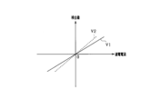
- FIG. 7 is a diagram showing detected values of voltages at a first detection point and a second detection point;
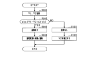
- FIG. 8 is a flowchart showing a monitoring process for a shunt resistor according to the first embodiment;
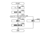
- FIG. 9 is a flowchart showing a method for monitoring a shunt resistor according to a modified example.
- FIG. 10 is a top view of a shunt resistor according to a second embodiment;
- FIG. 11 is a top view showing a resistor and each electrode of a shunt resistor according to a second embodiment;
- FIG. 12 is a cross-sectional view taken along line IIX-IIX of FIG. 11;
- FIG. 13 is a top view of a shunt resistor according to a third embodiment;
- FIG. 14 is a top view of a shunt resistor according to a fourth embodiment;
- FIG. 15 is a flowchart showing a monitoring process for a shunt resistor according to the fourth embodiment.
- FIG. 1 shows a power supply system 10 including a monitoring device 20 for a resistor 13 according to an embodiment.
- the power supply system 10 includes a storage battery 11, a resistor 13, a detection circuit 15, a monitoring device 20, a first relay RL1, and a second relay RL2.
- the resistor 13 is connected to the high potential side of the storage battery 11
- the first relay RL1 is connected to the high potential side of the resistor 13
- the second relay RL2 is connected to the low potential side of the storage battery 11, but the connection order is not limited thereto.
- the storage battery 11 may be connected between the first relay RL1 and the resistor 13.
- the power supply system 10 is connected to a load 30.
- the power supply system 10 is mounted on a vehicle, and the load 30 represents various electric loads mounted on the vehicle.
- the detection circuit 15 includes a first AD converter ADC1 and a second AD converter ADC2 connected in parallel to the resistor 13.
- the monitoring device 20 acquires the voltage across the resistor 13 from the detection circuit 15.
- the monitoring device 20 acquires a first voltage V1 as a detected voltage value from the first AD converter ADC1, and acquires a second voltage V2 as a detected voltage value from the second AD converter ADC2.
- the resistor 13 is a shunt resistor, and the monitoring device 20 detects the current flowing through the storage battery 11 by detecting the voltage across the resistor 13.
- FIGS. 2 to 5 show a shunt resistor 100 used as the resistor 13 shown in FIG. 1.
- FIG. 2 is an exploded perspective view of the shunt resistor 100
- FIG. 3 is a top view of the shunt resistor 100
- FIGS. 4 and 5 are cross-sectional views of the shunt resistor 100.
- the shunt resistor 100 comprises a plate-shaped first electrode 110 and a plate-shaped second electrode 120, a plate-shaped resistor 130, and a substrate 140.
- the material of the resistor 130 may be, for example, a nickel-chromium alloy, a copper-nickel alloy, a copper-manganese alloy, or a copper-manganese-nickel alloy, but is not limited to these.
- the first electrode 110 and the second electrode 120 may be, for example, a bus bar made of copper, but is not limited to these.
- the first electrode 110 and the second electrode 120 are provided with a first through hole 113 and a second through hole 123, respectively.
- the substrate 140 is a printed circuit board, and may be a rigid board made of glass or the like impregnated with epoxy resin, or a flexible board made of polyimide resin or the like.
- a wiring pattern is provided on the upper surface (the surface on the positive side of the z-axis) and the lower surface (the surface on the negative side of the z-axis) of the substrate 140.
- the first electrode 110 and the second electrode 120 are connected to both sides of the resistor 130 in a first direction (x-axis direction shown in FIG. 2) along the plate surface of the resistor 130.
- the positive x-axis surface of the first electrode 110 is joined to the negative x-axis surface of the resistor 130
- the negative x-axis surface of the second electrode 120 is joined to the positive x-axis surface of the resistor 130.
- a second direction y-axis direction shown in FIG. 2 perpendicular to the first direction
- the lengths of the first electrode 110, the second electrode 120, and the resistor 130 are approximately the same.
- the first electrode 110, the second electrode 120, and the resistor 130 are flat and approximately parallel to the xy plane shown in FIG. 2.
- the first electrode 110 and the second electrode 120 have approximately the same thickness in a third direction (z-axis direction shown in FIG. 2) perpendicular to the first and second directions.
- the thickness of the resistor 130 in the third direction is thinner than the thicknesses of the first electrode 110 and the second electrode 120.
- the first electrode 110, the second electrode 120, and the resistor 130 are aligned in the positive and negative directions of the y-axis and in the negative direction of the z-axis, and are joined by welding.
- the first electrode 110 and the resistor 130 are joined to each other via a first weld 111
- the second electrode 120 and the resistor 130 are joined to each other via a second weld 121.
- the first weld 111 and the second weld 121 correspond to conductive joints.
- the first electrode 110 and the resistor 130 are joined to each other and electrically connected to each other via the first weld 111.
- the second electrode 120 and the resistor 130 are joined to each other and electrically connected to each other via the second weld 121.
- a pair of first upper surface wirings 116, 126 and a pair of second upper surface wirings 117, 127 are provided on the upper surface of the substrate 140.
- a first bonding wiring 115 and a second bonding wiring 125 are provided on the lower surface of the substrate 140.
- a pair of first detection points 116h, 126h and a pair of second detection points 117h, 127h are provided on the upper and lower surfaces of the substrate 140.
- the first detection points 116h, 126h and the second detection points 117h, 127h are formed by wiring provided on the periphery and inner surface of a via hole that penetrates the substrate 140 in the vertical direction.
- the first detection points 116h, 126h are connected to the first top surface wirings 116, 126, respectively, and the second detection points 117h, 127h are connected to the second top surface wirings 117, 127, respectively.
- the first top surface wirings 116, 126 are connected to the first AD converter ADC1 of the detection circuit 15, and the second top surface wirings 117, 127 are connected to the second AD converter ADC2 of the detection circuit 15.
- the first detection point 116h and the second detection point 117h are connected to the first joining wiring 115 via the first underside wiring 116a and the second underside wiring 117a, respectively, and the first detection point 126h and the second detection point 127h are connected to the second joining wiring 125 via the first underside wiring 126a and the second underside wiring 127a, respectively.
- the first detection point 116h and the second detection point 117h are provided on the first electrode 110 side, and the first detection point 126h and the second detection point 127h are provided on the second electrode 120 side.
- the first detection points 116h, 126h are located approximately in the center of the first electrode 110 and the second electrode 120 in the y-axis direction.
- the second detection points 117h, 127h are located on the end side of the first electrode 110 and the second electrode 120 in the positive direction of the y-axis direction.
- the second detection points 117h, 127h are located on the end side of the first electrode 110 and the second electrode 120 in the y-axis direction from the first detection points 116h, 126h.
- the first upper surface wirings 116, 126 extend from the end of the substrate 140 in the negative direction of the y-axis along the positive direction of the y-axis, and have a shape that is bent toward the first detection points 116h, 126h, respectively.
- the second top surface wiring 117, 127 extends from the end of the substrate 140 in the negative direction of the y axis between the first top surface wiring 116, 126 along the positive direction of the y axis, and has a bent shape toward the second detection points 117h, 127h, respectively.
- the substrate 140 is joined to the first electrode 110 via the first solder portion 114 and to the second electrode 120 via the second solder portion 124.
- the first solder portion 114 is provided at a first solder position 112 on the upper surface of the first electrode 110 and is solder-joined such that the first bonding wire 115 of the substrate 140 is located on the upper surface of the first solder portion 114.
- the second solder portion 124 is provided at a second solder position 122 on the upper surface of the second electrode 120 and is solder-joined such that the second bonding wire 125 of the substrate 140 is located on the upper surface of the second solder portion 124.
- the thickness of the resistor 130 in the z direction is thinner than the thickness of the first electrode 110 and the second electrode 120, and they are aligned so that their faces in the negative direction of the z axis are aligned. Therefore, as shown in FIG. 5, the distance between the upper surface of the resistor 130 and the substrate 140 is wider than the distance between the upper surfaces of the first electrode 110 and the second electrode 120 and the substrate 140.
- the pair of first detection points 116h, 126h and the pair of second detection points 117h, 127h are provided at positions above the resistor 130.
- the first solder portion 114 and the second solder portion 124 correspond to conductive joints.
- the first electrode 110 and the substrate 140 are joined to each other via the first solder portion 114.
- the first electrode 110 and the first joint wiring 115 of the substrate 140 are electrically connected to each other via the first solder portion 114.
- the second electrode 120 and the substrate 140 are joined to each other via the second solder portion 124.
- the second electrode 120 and the second joint wiring 125 of the substrate 140 are electrically connected to each other via the second solder portion 124.
- the shunt resistor 100 can be manufactured, for example, by the following procedure. First, the first electrode 110, the second electrode 120, and the resistor 130 are prepared and welded together. Next, the first solder portion 114 is formed at the first solder position 112, and the second solder portion 124 is formed at the second solder position 122. Next, the substrate 140 on which a wiring pattern is formed is prepared, and the substrate 140 is aligned and soldered so that the first bonding wire 115 is located on the upper surface of the first solder portion 114, and the second bonding wire 125 is located on the upper surface of the second solder portion 124. In this way, the shunt resistor 100 can be manufactured.
- the first AD converter ADC1 is connected to the first upper surface wiring 116 and the first upper surface wiring 126, and detects the voltage across the first electrode 110 and the second electrode 120 of the resistor 130 as a first voltage V1.
- the current path (first current path) from the first top surface wiring 116 to the first top surface wiring 126 is in the following order: first top surface wiring 116, first detection point 116h (more specifically, from the top side to the bottom side of the first detection point 116h), first bottom surface wiring 116a, first bonding wiring 115, first solder portion 114, first electrode 110, first welding portion 111, resistor 130, second welding portion 121, second electrode 120, second solder portion 124, second bonding wiring 125, first bottom surface wiring 126a, first detection point 126h (more specifically, from the bottom side to the top side of the first detection point 126h), and first top surface wiring 126. Since the first detection points 116h and 126h are located approximately in the center of the first electrode 110 and the second electrode 120 in the y
- the second AD converter ADC2 is connected to the second upper surface wiring 117 and the second upper surface wiring 127, and detects the voltage across the first electrode 110 and the second electrode 120 of the resistor 130 as a second voltage V2.
- the current path (second current path) from the second upper surface wiring 117 to the second upper surface wiring 127 is in the following order: second upper surface wiring 117, second detection point 117h (more specifically, from the upper surface side to the lower surface side of the second detection point 117h), second lower surface wiring 117a, first bonding wiring 115, first solder portion 114, first electrode 110, first welding portion 111, resistor 130, second welding portion 121, second electrode 120, second solder portion 124, second bonding wiring 125, second lower surface wiring 127a, second detection point 127h (more specifically, from the lower surface side to the upper surface side of the second detection point 127h), and second upper surface wiring 127.
- the second current path is a path that passes through the positive end side of the resistor 130 in the y-axis direction.
- the monitoring device 20 includes a fault determination unit 21, a correction unit 22, and a control unit 23.
- the monitoring device 20 is mainly composed of a well-known microcomputer (microcomputer) including a CPU, a ROM, a RAM, a flash memory, and the like.
- the CPU executes a power conversion program installed in the ROM to realize the functions of the switching control unit 41 and the switching unit 42 of the control device 40.
- the functions provided by the microcomputer may be provided by software recorded in a physical memory device and a computer that executes the software, by software only, by hardware only, or by a combination of these.
- the microcomputer when the microcomputer is provided by an electronic circuit that is hardware, it can be provided by a digital circuit including a large number of logic circuits, or by an analog circuit.
- the microcomputer executes a program stored in a non-transitional physical recording medium as a storage unit provided by the microcomputer itself.
- the program includes, for example, a battery control processing program described later.
- a method corresponding to the program is executed.
- the storage unit is, for example, a non-volatile memory. Note that the program stored in the storage unit can be updated, for example, via a network such as the Internet.
- the fault determination unit 21 determines whether there is a connection abnormality in the conductive joints, that is, the first welded portion 111, the second welded portion 121, the first solder portion 114, and the second solder portion 124, based on the detected voltages of the first detection points 116h, 126h and the second detection points 117h, 127h.
- FIG. 6 is a diagram showing the current density distribution of the current flowing between the first and second electrodes 110, 120 and the resistor 130 in the shunt resistor 100.
- the vertical axis indicates the current density J
- the horizontal axis indicates the position in the y-axis direction of the first and second electrodes 110, 120.
- w is the length of the first and second electrodes 110, 120 in the y-axis direction
- the current density of the positive current flowing through the shunt resistor 100 is distributed in a downward convex curve that is lower toward the center of the first and second electrodes 110, 120 and higher toward the ends.
- FIG. 7 shows the current flowing between the first and second electrodes 110, 120 and the resistor 130 on the horizontal axis, and the voltage detection values detected by the first and second AD converters ADC1, ADC2 on the vertical axis. Even if the current flowing between the first and second electrodes 110, 120 and the resistor 130 is the same, the absolute value of the first voltage V1 detected by the first AD converter ADC1 will be smaller than the absolute value of the second voltage V2 detected by the second AD converter ADC2.
- junction abnormalities may occur at each conductive joint. Junction abnormalities are more likely to occur at positions with high current density than at positions with low current density for the same current flow. In other words, junction abnormalities are more likely to occur at each conductive joint at both ends of the first electrode 110 and the second electrode 120 in the y-axis direction, where the current density is high, than at the center of the first electrode 110 and the second electrode 120 in the y-axis direction, where the current density is low. Junction abnormalities that occur at both ends of the first electrode 110 and the second electrode 120 in the y-axis direction gradually spread toward the center.
- the second current path including the second detection points 117h and 127h in the resistor 130 approaches the first current path including the first detection points 116h and 126h.
- the value of the second voltage V2 gradually approaches the first voltage V1, and the difference between them becomes smaller.
- the fault determination unit 21 is configured to determine that a junction abnormality has occurred in any of the conductive junctions of the shunt resistor 100 when there is a change in the difference between the first voltage V1 and the second voltage V2. For example, the fault determination unit 21 is configured to determine that a junction abnormality has occurred when abs(V1-V2), which is the absolute value of the difference between the first voltage V1 and the second voltage V2, becomes equal to or less than a predetermined threshold voltage difference Vth (when abs(V1-V2) ⁇ Vth).
- the threshold voltage difference Vth can be set, for example, by measuring or calculating Vr, which is the absolute value of the difference between the first voltage V1 and the second voltage V2 when there is no junction abnormality in each conductive junction of the shunt resistor 100, so that 0 ⁇ Vth ⁇ Vr.
- Vr may be theoretically calculated based on the design value of the shunt resistor 100, or may be calculated using the first voltage V1 and the second voltage V2 measured using the shunt resistor 100 in an initial state.
- the correction unit 22 corrects at least one of the first voltage V1 and the second voltage V2 so that the first voltage V1 and the second voltage V2 are substantially the same.
- the correction unit 22 can correct the first voltage V1 and the second voltage V2 so that they are substantially the same, for example, by using the difference or ratio between the second voltage V2 and the first voltage V1.
- the correction unit 22 may correct the first voltage V1, but it is more preferable to correct the second voltage V2 because the second voltage V2 is a value that changes when a joint abnormality occurs at each conductive joint, whereas the first voltage V1 is a value that is unlikely to change even when a joint abnormality occurs at each conductive joint.
- the correction unit 22 may be configured to correct the first voltage V1 and the second voltage V2 to be substantially the same when the fault determination unit 21 determines that a connection abnormality has occurred. By comparing the first voltage V1 and the second voltage V2 in the corrected state, it is possible to determine, for example, faults in the first and second AD converters ADC1 and ADC2.
- the fault determination unit 21 may also be configured to be able to determine faults in the first and second AD converters ADC1 and ADC2.
- the correction unit 22 may correct the first voltage V1 and the second voltage V2 to be substantially the same, and then the fault determination unit 21 may compare the first voltage V1 and the second voltage V2 in the corrected state to determine that there is a junction abnormality.
- the fault determination unit 21 may be configured to determine that there is a junction abnormality when abs(V1-V2a), which is the absolute value of the difference between the first voltage V1 and the correction value V2a, becomes equal to or greater than a predetermined threshold voltage difference Vtha (when abs(V1-V2a) ⁇ Vtha).
- the control unit 23 executes opening and closing control of the first relay RL1 and the second relay RL2 based on at least one of the first voltage V1 and the second voltage V2 acquired from the detection circuit 15.
- the control unit 23 executes control to cut off the current flowing through the shunt resistor 100.
- the control unit 23 controls the first relay RL1 and the second relay RL2 to an open state, thereby cutting off the current flowing through the shunt resistor 100.
- control unit 23 may be configured to determine whether to limit or cut off the current flowing through the shunt resistor 100 and execute either control when the fault determination unit 21 determines that a joint abnormality has occurred.
- FIG. 8 is a flowchart of the monitoring process of the shunt resistor 100 executed by the monitoring device 20.
- the process shown in the flowchart in FIG. 8 is realized by the CPU constituting the monitoring device 20 executing a monitoring program installed in the ROM, and is executed repeatedly at predetermined intervals when the storage battery 11 is charged or discharged.
- step S101 the first voltage V1 and the second voltage V2 are obtained, and the process proceeds to step S102.
- step S102 if abs(V1-V2), which is the absolute value of the difference between the first voltage V1 and the second voltage V2, is equal to or less than a predetermined threshold voltage difference Vth (if abs(V1-V2) ⁇ Vth), it is determined that there is a junction abnormality, and the process proceeds to step S103. If abs(V1-V2)>Vth, it is determined that there is no junction abnormality, and the process proceeds to step S105.
- step S103 it is determined that there is a fault in the shunt resistor 100, and the process proceeds to step S104, where the current is limited or cut off.
- the monitoring device 20 controls the first relay RL1 and the second relay RL2 to an open state, and the process ends.
- the second detection points 117h and 127h are located on the substrate 140 closer to the end of each electrode than the first detection points 116h and 126h in the second direction. That is, the second detection points 117h and 127h are located on the end side where the current density of the current flowing between the first and second electrodes 110 and 120 and the resistor 130 is higher than the first detection points 116h and 126h.
- the monitoring device 20 executes the fault determination steps shown in steps S102, S103, and S105, and determines that there is a junction abnormality in the conductive junction of the shunt resistor 100 when abs(V1-V2) ⁇ Vth is satisfied based on abs(V1-V2), which is the absolute value of the difference between the first voltage V1 and the second voltage V2.
- the fault determination step makes it possible to monitor the conductive junction of the shunt resistor of the shunt resistor 100 for abnormalities.
- the correction step shown in step S106 is executed to correct the second voltage V2 to a correction value V2a that is substantially the same as the first voltage V1.
- the monitoring device 20 may be configured to execute the flowchart shown in Fig. 9 as a monitoring process for the shunt resistor 100.
- the process shown in the flowchart in Fig. 9 is realized by a CPU constituting the monitoring device 20 executing a monitoring program installed in a ROM, and is repeatedly executed at predetermined intervals when the storage battery 11 is charged or discharged.
- step S201 the first voltage V1 and the second voltage V2 are obtained, and the process proceeds to step S102.
- step S202 the second voltage V2 obtained in step S201 is corrected to a correction value V2a, and the process proceeds to step S203.
- step S203 it is determined whether abs(V1-V2a) ⁇ Vtha. If abs(V1-V2a) ⁇ Vtha, it is determined that there is a junction abnormality, and the process proceeds to step S204. If abs(V1-V2a)>Vtha, it is determined that there is no junction abnormality, and the process proceeds to step S205.
- step S204 it is determined that there is a fault in the shunt resistor 100, and the process proceeds to step S205, where the current is limited or cut off.
- the monitoring device 20 controls the first relay RL1 and the second relay RL2 to an open state, and ends the process.
- step S206 it is determined that there is no fault in the shunt resistor 100, and ends the process.
- FIG. 11 shows the shunt resistor 200 with the substrate 140 and the first and second solder parts 114, 124 removed.
- the first and second electrodes 110, 120 are connected to both sides of the resistor 230 by welding.
- FIG. 12 is a cross-sectional view of the resistor 230 shown in FIG. 11. As shown in FIGS. 10 and 11, the length of the resistor 230 in the y-axis direction is shorter than the length of the first and second electrodes 110, 120 in the y-axis direction.
- the resistor 230 and the first and second electrodes 110, 120 are connected so that their ends on the negative side of the y-axis are aligned, and at the end on the positive side of the y-axis, a non-existence part 250 where the resistor 230 is not present is provided between the first and second electrodes 110, 120. Also, as shown in FIG. 12, the resistor 230 is locally thin at the end on the positive side of the y-axis. The cross-sectional area of this thinned portion perpendicular to the x-axis is smaller than the cross-sectional area of the non-thinned portion perpendicular to the x-axis, and is therefore referred to as reduced section 231.
- the resistor 230 has a reduced section 231 with a reduced cross-sectional area perpendicular to the x-axis compared to the end side in the negative direction of the y-axis, due to the reduced length in the y-axis direction and the reduced length (thickness) in the z-axis direction at the end side in the positive direction of the y-axis.
- the x-axis direction is the direction of the current flowing between the first and second electrodes 110, 120 and the resistor 230, so that the current density at the reduced section 231 at the end side in the positive direction of the y-axis is higher than the current density at the end side in the negative direction of the y-axis in the resistor 230 due to the reduced cross-sectional area perpendicular to the x-axis. For this reason, junction abnormalities in each conductive junction of the shunt resistor 200 are more likely to occur from the reduced section 231 side, where the current density is higher.
- the second detection points 117h and 127h are provided on the substrate 140 located on the upper surface of the end side in the positive direction of the y axis where the reduced portion 231 is provided in the resistor 230, while the second detection points are not provided on the substrate 140 located on the upper surface of the end side in the negative direction of the y axis where the reduced portion is not provided.
- Third Embodiment Fig. 13 shows a shunt resistor 300 according to the third embodiment.
- the shunt resistor 300 is used as the resistor 13 shown in Fig. 1.
- the shunt resistor 300 differs from the shunt resistor 100 shown in Fig. 2 etc. in the form of the wiring pattern provided on the substrate 340.
- the same reference numbers are used for components similar to those of the shunt resistor 100.
- the first detection points 316h, 326h are provided at the same positions as the first detection points 116h, 126h in the shunt resistor 100.
- the second detection point 327h is provided at the same position as the second detection point 127h in the shunt resistor 100, while the second detection point 317h is provided on the negative side of the y-axis relative to the first detection point 316h, unlike the second detection point 117h in the shunt resistor 100.
- the first upper surface wiring 316, 326 is connected to the first detection points 316h, 326h, respectively, and the second upper surface wiring 117, 127 is connected to the second detection points 317h, 327h, respectively.
- the second detection points 317h, 327h are such that the second detection point 317h, which is one of the voltage detection points, is a detection point near the first end, which is the end in the positive direction of the y-axis on the first electrode 110 side, and the second detection point 327h, which is the other voltage detection point, is a detection point near the second end, which is the end in the negative direction of the y-axis on the opposite side to the first end on the second electrode 120 side.
- the first detection points 316h, 326h are arranged in a straight line along the x-axis direction, while the second detection points 317h, 327h are arranged approximately diagonally with respect to the resistor 230.
- the second detection points 317h, 327h are provided on the first end side and the second end side, respectively, even if a junction abnormality of each conductive junction provided in the shunt resistor 300 occurs from the first end side or the second end side, the value of the second voltage V2 gradually approaches the first voltage V1, and the difference between them becomes small, so that the occurrence of a junction abnormality can be detected.
- the shunt resistor 300 can reduce the number of voltage detection points installed and reliably detect junction abnormalities in each conductive junction of the shunt resistor 300.
- FIG. 14 shows a shunt resistor 400 according to the fourth embodiment.
- the shunt resistor 400 differs from the shunt resistor 100 shown in Fig. 2 etc. in the form of a wiring pattern provided on a substrate 440.
- the same reference numerals are used for components similar to those of the shunt resistor 100.
- a pair of first detection points 416h, 426h, a pair of second detection points 417h, 427h, and a pair of second detection points 418h, 428h are provided on the upper and lower surfaces of the substrate 440.
- the first detection points 416h, 426h, the second detection points 417h, 427h, and the second detection points 418h, 428h are formed by wiring provided on the periphery and inner surface of a via hole that penetrates the substrate 440 in the vertical direction.
- the first detection points 416h, 426h are provided at the same positions as the first detection points 116h, 126h in the shunt resistor 100.
- the first detection points 416h, 426h are provided at the same positions as the first detection points 116h, 126h in the shunt resistor 100.
- the second detection points 417h, 427h are provided at the same positions as the second detection points 117h, 127h in the shunt resistor 100.
- the second detection points 418h, 428h are located at the negative end side of the y-axis direction of the first electrode 110 and the second electrode 120.
- the distance between the second detection points 418h, 428h and the negative end of the y-axis direction of the first electrode 110 and the second electrode 120 is approximately the same as the distance between the second detection points 117h, 127h and the positive end of the y-axis direction of the first electrode 110 and the second electrode 120.
- the first top surface wiring 416, 426 is connected to the first detection points 416h, 426h, respectively
- the second top surface wiring 417, 427 is connected to the second detection points 417h, 427h, respectively
- the second top surface wiring 418, 428 is connected to the second detection points 418h, 428h, respectively.
- the shunt resistor 400 is used as the resistor 13 shown in FIG. 1, as in the first embodiment.
- the detection circuit 15 further includes a third AD converter ADC3.
- the third AD converter ADC3 is connected to the first top wiring 418 and the first top wiring 428, and detects the voltage across the first electrode 110 and the second electrode 120 of the resistive body 130 of the shunt resistor 400 as a third voltage V3.
- FIG. 15 is a flowchart of the monitoring process of the shunt resistor 400 executed by the monitoring device 20.
- the process shown in the flowchart in FIG. 15 is realized by the CPU constituting the monitoring device 20 executing a monitoring program installed in the ROM, and is executed repeatedly at predetermined intervals when the storage battery 11 is charged or discharged.
- step S301 the first voltage V1, the second voltage V2, and the third voltage V3 are obtained, and the process proceeds to step S302.
- step S302 if abs(V1-V2) ⁇ Vth2 or abs(V1-V3) ⁇ Vth3 holds for the predetermined threshold voltage differences Vth2 and Vth3, it is determined that there is a junction abnormality, and the process proceeds to step S303. If abs(V1-V2)>Vth2 and abs(V1-V3)>Vth3, it is determined that there is no junction abnormality, and the process proceeds to step S305.
- the threshold voltage differences Vth2 and Vth3 can be set by the same method as the threshold voltage difference Vth according to the first embodiment.
- step S303 it is determined that there is a fault in the shunt resistor 400, and the process proceeds to step S404, where the current is limited or cut off.
- the monitoring device 20 controls the first relay RL1 and the second relay RL2 to an open state, and ends the process.
- step S305 it is determined that there is no fault in the shunt resistor 400, and the process proceeds to step S406, where the second voltage V2 and the third voltage V3 are corrected, and the process ends.
- the second detection points 417h, 427h are provided on the positive end side of the first electrode 110 and the second electrode 120 in the y-axis direction
- the second detection points 418h, 428h are provided on the negative end side of the first electrode 110 and the second electrode 120 in the y-axis direction. Therefore, when a joint abnormality occurs at the positive end side of the conductive joints of the shunt resistor 400 in the y-axis direction, the value of the second voltage V2 gradually approaches the first voltage V1, and the difference between them becomes small, so that the occurrence of the joint abnormality can be detected.
- the resistor provided in the shunt resistor 400 may be configured to have the same structure as the reduction section 231 according to the third embodiment.
- the reduction section 231 may be provided on the end sides of the first electrode 110 and the second electrode 120 in the positive and negative directions of the y axis. By providing the reduction section 231 to increase the current density, the change in the detection voltage at the second detection point located on the upper surface can be detected with high sensitivity.
- the first and second solder parts 114, 124 extend continuously from one end side to the other end side of the first and second electrodes 110, 120 in the y-axis direction, respectively, but may be divided into multiple parts.
- the control unit 23 determines to limit or cut off the current flowing through the shunt resistor, but this is not limited to the above.
- the control unit 23 may be configured to immediately cut off the current flowing through the shunt resistor without relying on software for determination.
- control unit and the method described in the present disclosure may be realized by a dedicated computer provided by configuring a processor and memory programmed to execute one or more functions embodied in a computer program.
- control unit and the method described in the present disclosure may be realized by a dedicated computer provided by configuring a processor with one or more dedicated hardware logic circuits.
- control unit and the method described in the present disclosure may be realized by one or more dedicated computers configured by combining a processor and memory programmed to execute one or more functions with a processor configured with one or more hardware logic circuits.
- the computer program may be stored in a computer-readable non-transient tangible recording medium as instructions executed by the computer.
- the present invention is applied to a shunt resistor (100, 200, 300, 400) in which the resistor and each of the electrodes, and the electrodes and the substrate are joined by conductive joints (111, 121, 114, 124) along a second direction perpendicular to the first direction,
- a reduced portion (231) is provided at an end in the second direction, where the resistor is not present between the first electrode and the second electrode, or where the resistor is locally thinned, 2.
- the shunt resistor is provided with the reduced portion only at one end side of both ends in the second direction, The shunt resistor monitoring device according to configuration 2, wherein the second detection points are provided on the substrate only near the end on the reduced portion side of both ends in the second direction.
- the second detection point is a detection point of the pair of voltage detection points, one of which is a detection point near a first end in the second direction on the first electrode side, and the other voltage detection point is a detection point near a second end on the opposite side to the first end in the second direction.
- [Configuration 5] 3. The shunt resistor monitoring device according to claim 1, wherein the second detection points are provided on the substrate on both sides of the first detection point in the second direction.
- the resistor and each electrode, and the electrodes and the substrate are joined by conductive joints (111, 121, 114, 124) along a second direction perpendicular to the first direction, a monitoring program for a shunt resistor (100, 200, 300, 400) in which first detection points (116h, 126h, 316h, 326h, 416h, 426h) and
- the resistor and each electrode, and the electrodes and the substrate are joined by conductive joints (111, 121, 114, 124) along a second direction perpendicular to the first direction,
- the substrate is provided with a pair of voltage detection points, including first detection points (116h, 126h, 316h, 326h, 416h, 426h) and second detection points (117h, 127
Landscapes
- Physics & Mathematics (AREA)
- General Physics & Mathematics (AREA)
- Measuring Instrument Details And Bridges, And Automatic Balancing Devices (AREA)
- Measurement Of Current Or Voltage (AREA)
Priority Applications (3)
| Application Number | Priority Date | Filing Date | Title |
|---|---|---|---|
| DE112024001314.7T DE112024001314T5 (de) | 2023-03-20 | 2024-03-07 | Shunt-Widerstandseinrichtung, Überwachungseinrichtung für Shunt-Widerstandseinrichtung und Überwachungsprogramm für Shunt-Widerstandseinrichtung |
| CN202480019091.5A CN120883065A (zh) | 2023-03-20 | 2024-03-07 | 分流电阻器、分流电阻器的监视装置和分流电阻器的监视程序 |
| US19/326,274 US20260009867A1 (en) | 2023-03-20 | 2025-09-11 | Shunt resistor device, monitoring device for shunt resistor device, and storage medium |
Applications Claiming Priority (2)
| Application Number | Priority Date | Filing Date | Title |
|---|---|---|---|
| JP2023-044735 | 2023-03-20 | ||
| JP2023044735A JP7831366B2 (ja) | 2023-03-20 | 2023-03-20 | シャント抵抗器、シャント抵抗器の監視装置及びシャント抵抗器の監視プログラム |
Related Child Applications (1)
| Application Number | Title | Priority Date | Filing Date |
|---|---|---|---|
| US19/326,274 Continuation US20260009867A1 (en) | 2023-03-20 | 2025-09-11 | Shunt resistor device, monitoring device for shunt resistor device, and storage medium |
Publications (1)
| Publication Number | Publication Date |
|---|---|
| WO2024195564A1 true WO2024195564A1 (ja) | 2024-09-26 |
Family
ID=92842000
Family Applications (1)
| Application Number | Title | Priority Date | Filing Date |
|---|---|---|---|
| PCT/JP2024/008749 Ceased WO2024195564A1 (ja) | 2023-03-20 | 2024-03-07 | シャント抵抗器、シャント抵抗器の監視装置及びシャント抵抗器の監視プログラム |
Country Status (5)
| Country | Link |
|---|---|
| US (1) | US20260009867A1 (https=) |
| JP (1) | JP7831366B2 (https=) |
| CN (1) | CN120883065A (https=) |
| DE (1) | DE112024001314T5 (https=) |
| WO (1) | WO2024195564A1 (https=) |
Citations (6)
| Publication number | Priority date | Publication date | Assignee | Title |
|---|---|---|---|---|
| JP2016514841A (ja) * | 2013-04-05 | 2016-05-23 | イザベレンヒュッテ ホイスラー ゲー・エム・ベー・ハー ウント コンパニー コマンデイトゲゼルシャフト | 測定用抵抗器、および対応する測定方法 |
| WO2017135024A1 (ja) * | 2016-02-01 | 2017-08-10 | パナソニックIpマネジメント株式会社 | バッテリーセンサー装置 |
| JP2019531469A (ja) * | 2016-08-17 | 2019-10-31 | イザベレンヒュッテ ホイスラー ゲー・エム・ベー・ハー ウント コンパニー コマンデイトゲゼルシャフト | 大電流範囲の電流を測定するための測定装置 |
| JP2021174802A (ja) * | 2020-04-20 | 2021-11-01 | Koa株式会社 | シャント抵抗器 |
| JP2022123429A (ja) * | 2021-02-12 | 2022-08-24 | Koa株式会社 | シャント抵抗器と電圧信号検出基板との接続方法、および電流検出装置 |
| JP2022177468A (ja) * | 2021-05-18 | 2022-12-01 | Koa株式会社 | 電流検出装置 |
-
2023
- 2023-03-20 JP JP2023044735A patent/JP7831366B2/ja active Active
-
2024
- 2024-03-07 WO PCT/JP2024/008749 patent/WO2024195564A1/ja not_active Ceased
- 2024-03-07 DE DE112024001314.7T patent/DE112024001314T5/de active Pending
- 2024-03-07 CN CN202480019091.5A patent/CN120883065A/zh active Pending
-
2025
- 2025-09-11 US US19/326,274 patent/US20260009867A1/en active Pending
Patent Citations (6)
| Publication number | Priority date | Publication date | Assignee | Title |
|---|---|---|---|---|
| JP2016514841A (ja) * | 2013-04-05 | 2016-05-23 | イザベレンヒュッテ ホイスラー ゲー・エム・ベー・ハー ウント コンパニー コマンデイトゲゼルシャフト | 測定用抵抗器、および対応する測定方法 |
| WO2017135024A1 (ja) * | 2016-02-01 | 2017-08-10 | パナソニックIpマネジメント株式会社 | バッテリーセンサー装置 |
| JP2019531469A (ja) * | 2016-08-17 | 2019-10-31 | イザベレンヒュッテ ホイスラー ゲー・エム・ベー・ハー ウント コンパニー コマンデイトゲゼルシャフト | 大電流範囲の電流を測定するための測定装置 |
| JP2021174802A (ja) * | 2020-04-20 | 2021-11-01 | Koa株式会社 | シャント抵抗器 |
| JP2022123429A (ja) * | 2021-02-12 | 2022-08-24 | Koa株式会社 | シャント抵抗器と電圧信号検出基板との接続方法、および電流検出装置 |
| JP2022177468A (ja) * | 2021-05-18 | 2022-12-01 | Koa株式会社 | 電流検出装置 |
Also Published As
| Publication number | Publication date |
|---|---|
| US20260009867A1 (en) | 2026-01-08 |
| CN120883065A (zh) | 2025-10-31 |
| JP2024134432A (ja) | 2024-10-03 |
| JP7831366B2 (ja) | 2026-03-17 |
| DE112024001314T5 (de) | 2025-12-31 |
Similar Documents
| Publication | Publication Date | Title |
|---|---|---|
| US10473695B2 (en) | Current detection device | |
| US9437352B2 (en) | Resistor and structure for mounting same | |
| CN104115241B (zh) | 电阻器的端子连接构造 | |
| JP6854143B2 (ja) | シャント抵抗器およびシャント抵抗器を用いた電流検出装置 | |
| JP5619663B2 (ja) | シャント抵抗器の接続端子、及びバッテリー状態検知装置 | |
| JP6384211B2 (ja) | シャント抵抗器 | |
| US10969408B2 (en) | Current measuring device | |
| TWI865709B (zh) | 電阻器陣列、具有電阻器陣列的測量電路以及製造用於電阻器陣列的帶狀材料複合體的方法 | |
| US20180100877A1 (en) | Current detection device | |
| KR20130106830A (ko) | 전류 감응형 저항기 | |
| US20190295749A1 (en) | Shunt resistor and mounted structure of shunt resistor | |
| US10641798B2 (en) | Current detection device having a fixing portion formed in a wiring member | |
| JP6462233B2 (ja) | 電流検出構造 | |
| US20120170164A1 (en) | Overcurrent cutoff device, and overcurrent detecting element to be used in overcurrent cutoff device | |
| WO2021235229A1 (ja) | シャント抵抗器およびその製造方法 | |
| JP7074722B2 (ja) | センサ | |
| US20170122985A1 (en) | Shunt resistor | |
| JP6564482B2 (ja) | 金属板抵抗器 | |
| WO2024195564A1 (ja) | シャント抵抗器、シャント抵抗器の監視装置及びシャント抵抗器の監視プログラム | |
| US11536771B2 (en) | Current sensor | |
| US11268866B2 (en) | Charge amplifier, force sensor, and robot | |
| JP7490351B2 (ja) | シャント抵抗モジュール及び、シャント抵抗モジュールの実装構造 | |
| CN110622017B (zh) | 用于电蓄能单元的状态识别的分流电阻 | |
| JPH1056130A (ja) | 半導体装置 | |
| JP2009097860A (ja) | 電気接続方法および電気接続装置 |
Legal Events
| Date | Code | Title | Description |
|---|---|---|---|
| 121 | Ep: the epo has been informed by wipo that ep was designated in this application |
Ref document number: 24774703 Country of ref document: EP Kind code of ref document: A1 |
|
| WWE | Wipo information: entry into national phase |
Ref document number: CN2024800190915 Country of ref document: CN Ref document number: 202480019091.5 Country of ref document: CN |
|
| WWE | Wipo information: entry into national phase |
Ref document number: 112024001314 Country of ref document: DE |
|
| WWP | Wipo information: published in national office |
Ref document number: 202480019091.5 Country of ref document: CN |
|
| WWP | Wipo information: published in national office |
Ref document number: 112024001314 Country of ref document: DE |
|
| 122 | Ep: pct application non-entry in european phase |
Ref document number: 24774703 Country of ref document: EP Kind code of ref document: A1 |