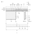
WO2024195460A1 - 半導体装置 - Google Patents
半導体装置 Download PDFInfo
- Publication number
- WO2024195460A1 WO2024195460A1 PCT/JP2024/007379 JP2024007379W WO2024195460A1 WO 2024195460 A1 WO2024195460 A1 WO 2024195460A1 JP 2024007379 W JP2024007379 W JP 2024007379W WO 2024195460 A1 WO2024195460 A1 WO 2024195460A1
- Authority
- WO
- WIPO (PCT)
- Prior art keywords
- region
- emitter
- trench
- gate
- diode
- Prior art date
- Legal status (The legal status is an assumption and is not a legal conclusion. Google has not performed a legal analysis and makes no representation as to the accuracy of the status listed.)
- Ceased
Links
Images







Classifications
-
- H—ELECTRICITY
- H10—SEMICONDUCTOR DEVICES; ELECTRIC SOLID-STATE DEVICES NOT OTHERWISE PROVIDED FOR
- H10D—INORGANIC ELECTRIC SEMICONDUCTOR DEVICES
- H10D62/00—Semiconductor bodies, or regions thereof, of devices having potential barriers
- H10D62/10—Shapes, relative sizes or dispositions of the regions of the semiconductor bodies; Shapes of the semiconductor bodies
-
- H—ELECTRICITY
- H10—SEMICONDUCTOR DEVICES; ELECTRIC SOLID-STATE DEVICES NOT OTHERWISE PROVIDED FOR
- H10D—INORGANIC ELECTRIC SEMICONDUCTOR DEVICES
- H10D84/00—Integrated devices formed in or on semiconductor substrates that comprise only semiconducting layers, e.g. on Si wafers or on GaAs-on-Si wafers
- H10D84/101—Integrated devices comprising main components and built-in components, e.g. IGBT having built-in freewheel diode
- H10D84/161—IGBT having built-in components
-
- H—ELECTRICITY
- H10—SEMICONDUCTOR DEVICES; ELECTRIC SOLID-STATE DEVICES NOT OTHERWISE PROVIDED FOR
- H10D—INORGANIC ELECTRIC SEMICONDUCTOR DEVICES
- H10D12/00—Bipolar devices controlled by the field effect, e.g. insulated-gate bipolar transistors [IGBT]
- H10D12/01—Manufacture or treatment
- H10D12/031—Manufacture or treatment of IGBTs
- H10D12/032—Manufacture or treatment of IGBTs of vertical IGBTs
- H10D12/038—Manufacture or treatment of IGBTs of vertical IGBTs having a recessed gate, e.g. trench-gate IGBTs
-
- H—ELECTRICITY
- H10—SEMICONDUCTOR DEVICES; ELECTRIC SOLID-STATE DEVICES NOT OTHERWISE PROVIDED FOR
- H10D—INORGANIC ELECTRIC SEMICONDUCTOR DEVICES
- H10D12/00—Bipolar devices controlled by the field effect, e.g. insulated-gate bipolar transistors [IGBT]
- H10D12/411—Insulated-gate bipolar transistors [IGBT]
- H10D12/417—Insulated-gate bipolar transistors [IGBT] having a drift region having a doping concentration that is higher at the collector side relative to other parts of the drift region
-
- H—ELECTRICITY
- H10—SEMICONDUCTOR DEVICES; ELECTRIC SOLID-STATE DEVICES NOT OTHERWISE PROVIDED FOR
- H10D—INORGANIC ELECTRIC SEMICONDUCTOR DEVICES
- H10D12/00—Bipolar devices controlled by the field effect, e.g. insulated-gate bipolar transistors [IGBT]
- H10D12/411—Insulated-gate bipolar transistors [IGBT]
- H10D12/418—Insulated-gate bipolar transistors [IGBT] having a drift region having a doping concentration that is higher at the emitter side relative to other parts of the drift region
-
- H—ELECTRICITY
- H10—SEMICONDUCTOR DEVICES; ELECTRIC SOLID-STATE DEVICES NOT OTHERWISE PROVIDED FOR
- H10D—INORGANIC ELECTRIC SEMICONDUCTOR DEVICES
- H10D12/00—Bipolar devices controlled by the field effect, e.g. insulated-gate bipolar transistors [IGBT]
- H10D12/411—Insulated-gate bipolar transistors [IGBT]
- H10D12/441—Vertical IGBTs
- H10D12/461—Vertical IGBTs having non-planar surfaces, e.g. having trenches, recesses or pillars in the surfaces of the emitter, base or collector regions
- H10D12/481—Vertical IGBTs having non-planar surfaces, e.g. having trenches, recesses or pillars in the surfaces of the emitter, base or collector regions having gate structures on slanted surfaces, on vertical surfaces, or in grooves, e.g. trench gate IGBTs
-
- H—ELECTRICITY
- H10—SEMICONDUCTOR DEVICES; ELECTRIC SOLID-STATE DEVICES NOT OTHERWISE PROVIDED FOR
- H10D—INORGANIC ELECTRIC SEMICONDUCTOR DEVICES
- H10D30/00—Field-effect transistors [FET]
- H10D30/60—Insulated-gate field-effect transistors [IGFET]
-
- H—ELECTRICITY
- H10—SEMICONDUCTOR DEVICES; ELECTRIC SOLID-STATE DEVICES NOT OTHERWISE PROVIDED FOR
- H10D—INORGANIC ELECTRIC SEMICONDUCTOR DEVICES
- H10D62/00—Semiconductor bodies, or regions thereof, of devices having potential barriers
- H10D62/10—Shapes, relative sizes or dispositions of the regions of the semiconductor bodies; Shapes of the semiconductor bodies
- H10D62/102—Constructional design considerations for preventing surface leakage or controlling electric field concentration
- H10D62/103—Constructional design considerations for preventing surface leakage or controlling electric field concentration for increasing or controlling the breakdown voltage of reverse-biased devices
-
- H—ELECTRICITY
- H10—SEMICONDUCTOR DEVICES; ELECTRIC SOLID-STATE DEVICES NOT OTHERWISE PROVIDED FOR
- H10D—INORGANIC ELECTRIC SEMICONDUCTOR DEVICES
- H10D62/00—Semiconductor bodies, or regions thereof, of devices having potential barriers
- H10D62/10—Shapes, relative sizes or dispositions of the regions of the semiconductor bodies; Shapes of the semiconductor bodies
- H10D62/124—Shapes, relative sizes or dispositions of the regions of semiconductor bodies or of junctions between the regions
- H10D62/126—Top-view geometrical layouts of the regions or the junctions
- H10D62/127—Top-view geometrical layouts of the regions or the junctions of cellular field-effect devices, e.g. multicellular DMOS transistors or IGBTs
-
- H—ELECTRICITY
- H10—SEMICONDUCTOR DEVICES; ELECTRIC SOLID-STATE DEVICES NOT OTHERWISE PROVIDED FOR
- H10D—INORGANIC ELECTRIC SEMICONDUCTOR DEVICES
- H10D62/00—Semiconductor bodies, or regions thereof, of devices having potential barriers
- H10D62/60—Impurity distributions or concentrations
-
- H—ELECTRICITY
- H10—SEMICONDUCTOR DEVICES; ELECTRIC SOLID-STATE DEVICES NOT OTHERWISE PROVIDED FOR
- H10D—INORGANIC ELECTRIC SEMICONDUCTOR DEVICES
- H10D64/00—Electrodes of devices having potential barriers
- H10D64/111—Field plates
- H10D64/117—Recessed field plates, e.g. trench field plates or buried field plates
-
- H—ELECTRICITY
- H10—SEMICONDUCTOR DEVICES; ELECTRIC SOLID-STATE DEVICES NOT OTHERWISE PROVIDED FOR
- H10D—INORGANIC ELECTRIC SEMICONDUCTOR DEVICES
- H10D64/00—Electrodes of devices having potential barriers
- H10D64/20—Electrodes characterised by their shapes, relative sizes or dispositions
- H10D64/23—Electrodes carrying the current to be rectified, amplified, oscillated or switched, e.g. sources, drains, anodes or cathodes
- H10D64/232—Emitter electrodes for IGBTs
-
- H—ELECTRICITY
- H10—SEMICONDUCTOR DEVICES; ELECTRIC SOLID-STATE DEVICES NOT OTHERWISE PROVIDED FOR
- H10D—INORGANIC ELECTRIC SEMICONDUCTOR DEVICES
- H10D8/00—Diodes
- H10D8/422—PN diodes having the PN junctions in mesas
-
- H—ELECTRICITY
- H10—SEMICONDUCTOR DEVICES; ELECTRIC SOLID-STATE DEVICES NOT OTHERWISE PROVIDED FOR
- H10D—INORGANIC ELECTRIC SEMICONDUCTOR DEVICES
- H10D62/00—Semiconductor bodies, or regions thereof, of devices having potential barriers
- H10D62/10—Shapes, relative sizes or dispositions of the regions of the semiconductor bodies; Shapes of the semiconductor bodies
- H10D62/102—Constructional design considerations for preventing surface leakage or controlling electric field concentration
- H10D62/103—Constructional design considerations for preventing surface leakage or controlling electric field concentration for increasing or controlling the breakdown voltage of reverse-biased devices
- H10D62/105—Constructional design considerations for preventing surface leakage or controlling electric field concentration for increasing or controlling the breakdown voltage of reverse-biased devices by having particular doping profiles, shapes or arrangements of PN junctions; by having supplementary regions, e.g. junction termination extension [JTE]
- H10D62/106—Constructional design considerations for preventing surface leakage or controlling electric field concentration for increasing or controlling the breakdown voltage of reverse-biased devices by having particular doping profiles, shapes or arrangements of PN junctions; by having supplementary regions, e.g. junction termination extension [JTE] having supplementary regions doped oppositely to or in rectifying contact with regions of the semiconductor bodies, e.g. guard rings with PN or Schottky junctions
-
- H—ELECTRICITY
- H10—SEMICONDUCTOR DEVICES; ELECTRIC SOLID-STATE DEVICES NOT OTHERWISE PROVIDED FOR
- H10D—INORGANIC ELECTRIC SEMICONDUCTOR DEVICES
- H10D62/00—Semiconductor bodies, or regions thereof, of devices having potential barriers
- H10D62/10—Shapes, relative sizes or dispositions of the regions of the semiconductor bodies; Shapes of the semiconductor bodies
- H10D62/124—Shapes, relative sizes or dispositions of the regions of semiconductor bodies or of junctions between the regions
- H10D62/126—Top-view geometrical layouts of the regions or the junctions
-
- H—ELECTRICITY
- H10—SEMICONDUCTOR DEVICES; ELECTRIC SOLID-STATE DEVICES NOT OTHERWISE PROVIDED FOR
- H10D—INORGANIC ELECTRIC SEMICONDUCTOR DEVICES
- H10D62/00—Semiconductor bodies, or regions thereof, of devices having potential barriers
- H10D62/10—Shapes, relative sizes or dispositions of the regions of the semiconductor bodies; Shapes of the semiconductor bodies
- H10D62/129—Cathode regions of diodes
Definitions
- This disclosure relates to a semiconductor device including an IGBT region and a diode region.
- Patent Document 1 discloses an RC-IGBT (Reverse Conducting-Insulated Gate Bipolar Transistor) as an example of a semiconductor device.
- the RC-IGBT includes an IGBT region and a diode region fabricated in a common semiconductor layer.
- the IGBT region includes an IGBT.
- the diode region includes a diode.
- One embodiment of the present disclosure provides a semiconductor device that can suppress the snapback phenomenon.
- One embodiment of the present disclosure provides a semiconductor device including a semiconductor layer having a first main surface and a second main surface opposite the first main surface, an IGBT region formed in the semiconductor layer, a diode region formed in the semiconductor layer and adjacent to the IGBT region in a first direction, a plurality of gate trenches formed in the IGBT region and extending in a second direction intersecting the first direction, a gate conductive layer embedded in the gate trenches via a gate insulating layer, unit cells partitioned between the gate trenches formed at intervals in the first direction, and an emitter region formed in the first main surface of each of the unit cells.
- the area of the emitter region formed in the first unit cell relatively close to the diode region is smaller than the area of the emitter region formed in the second unit cell farther from the diode region than the first unit cell.
- a semiconductor device capable of suppressing the snapback phenomenon can be provided.
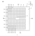
- FIG. 1 is a schematic plan view of a semiconductor device according to a first embodiment of the present disclosure.
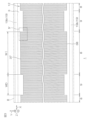
- FIG. 2 is a plan view showing a schematic structure of a first main surface of the semiconductor device.
- FIG. 3 is an enlarged view of a portion surrounded by a dashed line III in FIG.
- FIG. 4 is an enlarged view of a portion enclosed by a dashed line IV in FIG.
- FIG. 5 is an enlarged view of a portion surrounded by a dashed line V in FIG.
- FIG. 6 is an enlarged view of a portion surrounded by a dashed line VI in FIG.
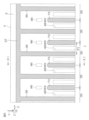
- FIG. 7A is an enlarged view of a portion surrounded by a dashed line VIIA in FIG.
- FIG. 7B is an enlarged view of the portion surrounded by the dashed line VIIB in FIG.
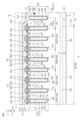
- FIG. 8 is a cross-sectional view taken along line VIII-VIII in FIG. 7A.
- FIG. 9 is a cross-sectional view taken along line IX-IX in FIG. 7A.
- FIG. 10 is a cross-sectional view taken along line X-X of FIG. 7A.
- FIG. 11 is a cross-sectional view taken along line XI-XI in FIG.
- FIG. 12 is a cross-sectional view of a semiconductor device according to the second embodiment of the present disclosure.
- FIG. 13 is an enlarged view of a semiconductor device according to a third embodiment of the present disclosure, and corresponds to FIG. 7A.
- FIG. 14 is a cross-sectional view taken along line XIV-XIV in FIG.
- FIG. 15 is an enlarged view of a semiconductor device according to a fourth embodiment of the present disclosure, and corresponds to FIG.
- FIG. 16 is an enlarged view of a portion surrounded by a dashed line XVI in FIG.
- FIG. 17 is an enlarged view of a portion surrounded by a dashed line XVII in FIG. 18 is a cross-sectional view taken along line XVIII-XVIII in FIG. 16.
- FIG. FIG. 19 is a cross-sectional view taken along line XIX-XIX in FIG.
- FIG. 1 is a schematic plan view of a semiconductor device 1 according to a first embodiment of the present disclosure.
- FIG. 2 is a schematic plan view showing the structure of a first main surface 3 of the semiconductor device 1.
- FIG. 3 is an enlarged view of a portion surrounded by a dashed dotted line III in FIG. 1.
- the semiconductor device 1 is an electronic component having an RC-IGBT (Reverse Conducting-Insulated Gate Bipolar Transistor) that has an IGBT and a diode integrated together.
- RC-IGBT Reverse Conducting-Insulated Gate Bipolar Transistor
- the semiconductor device 1 includes a semiconductor layer 2 having a rectangular parallelepiped shape.
- the semiconductor layer 2 has a first main surface 3 on one side, a second main surface 4 on the other side, and side surfaces 5A, 5B, 5C, and 5D that connect the first main surface 3 and the second main surface 4.
- the first principal surface 3 and the second principal surface 4 are formed in a quadrangular shape in a plan view (hereinafter simply referred to as "plan view") seen from their normal direction Z.
- the side surface 5A and the side surface 5C extend along the first direction X and face each other in a second direction Y that intersects with the first direction X.
- the side surface 5B and the side surface 5D extend along the second direction Y and face each other in the first direction X.
- the second direction Y is perpendicular to the first direction X.
- the semiconductor layer 2 includes an active region 6 and an outer region 7.
- the active region 6 is a region in which an RC-IGBT is formed.
- the active region 6 is set in the center of the semiconductor layer 2, spaced from the side surfaces 5A to 5D toward the inner region in a plan view.
- the active region 6 may be set in a rectangular shape having four sides parallel to the side surfaces 5A to 5D in a plan view.
- the thickness of the semiconductor layer 2 may be 50 ⁇ m or more and 200 ⁇ m or less.
- the outer region 7 is the region outside the active region 6.
- the outer region 7 extends in a band shape along the periphery of the active region 6 in a planar view. Specifically, the outer region 7 is endless (square ring shape) surrounding the active region 6 in a planar view.
- the active region 6 includes an IGBT region 8 and a diode region 9.
- the IGBT region 8 is shown by hatching for clarity.
- the IGBT region 8 is the region in which an IGBT is formed.
- the diode region 9 is the region in which a diode is formed.
- the diode region 9 is adjacent to the IGBT region 8.
- the active region 6 specifically includes an RC-IGBT array 12.
- a plurality of RC-IGBT arrays 12 are formed at intervals in the second direction Y.
- the RC-IGBT array 12 has a first end on one side (side surface 5B side) and a second end on the other side (side surface 5D side).
- the RC-IGBT array 12 has a loop arrangement including repeated IGBT regions 8, diode regions 9, IGBT regions 8, diode regions 9, etc., arranged in a line along the first direction X from the first end to the second end.
- the first end of the RC-IGBT array 12 is formed by the IGBT region 8.
- the first end of the RC-IGBT array 12 may be formed by the diode region 9.
- the second end of the RC-IGBT array 12 is formed by the IGBT region 8.
- the second end of the RC-IGBT array 12 may be formed by the diode region 9.
- a plurality of IGBT regions 8 are dispersed and arranged.
- the IGBT regions 8 are formed at intervals along the first direction X and the second direction Y.
- the IGBT regions 8 are arranged in a matrix in a planar view.
- the IGBT regions 8 face each other along the first direction X and face each other along the second direction Y.
- each of the IGBT regions 8 is formed in a rectangular shape extending along the second direction Y.
- a plurality of diode regions 9 are distributed and arranged in the active region 6. Specifically, the plurality of diode regions 9 are each formed so as to be adjacent to the IGBT region 8 in the first direction X. The plurality of diode regions 9 are formed at intervals along the first direction X and the second direction Y. In this embodiment, the plurality of diode regions 9 are arranged in a matrix in a plan view. The plurality of diode regions 9 face each other along the first direction X and face each other along the second direction Y. Specifically, the plurality of diode regions 9 are each formed in a rectangular shape extending along the second direction Y. The planar area of each diode region 9 may be equal to or smaller than the planar area of each IGBT region 8. It is preferable that the planar area of each diode region 9 is smaller than the planar area of each IGBT region 8.
- the width WI of each IGBT region 8 may be 10 ⁇ m or more and 1000 ⁇ m or less.
- the width WI may be 100 ⁇ m or more. It is preferable that the width WI is 200 ⁇ m or more.
- the width WD of each diode region 9 may be less than or equal to the width WI of each IGBT region 8.
- the width WD is the width of the diode region 9 in the first direction X. It is preferable that the width WD of each diode region 9 is less than the width WI of each IGBT region 8.
- the active area 6 further includes a sensor area 11 in which a temperature sensor is formed.
- the sensor area 11 is formed in a region between two RC-IGBT arrays 12 adjacent to each other in the second direction Y. In this embodiment, the sensor area 11 is formed in the center of the active area 6.
- the semiconductor device 1 further includes an emitter terminal electrode 13 (see the dashed line in FIG. 1).
- the emitter terminal electrode 13 is formed on the first main surface 3 of the semiconductor layer 2 in the active region 6.
- the emitter terminal electrode 13 transmits an emitter signal to the active region 6 (IGBT region 8).
- the emitter signal may be a reference potential or a ground potential.
- the semiconductor device 1 further includes a plurality of terminal electrodes 14, 15, 16, 17, and 18 (five in this embodiment) formed on the first main surface 3 of the semiconductor layer 2 in the outer region 7.
- the multiple terminal electrodes 14 to 18 are arranged at intervals from one another along the side surface 5D.
- the multiple terminal electrodes 14 to 18 are formed in a quadrangular shape in a plan view.
- the multiple terminal electrodes 14 to 18 include a gate terminal electrode 14, a first sense terminal electrode 15, a second sense terminal electrode 16, a current detection terminal electrode 17, and an open terminal electrode 18.
- the gate terminal electrode 14 transmits a gate signal to the active region 6 (IGBT region 8).
- the first sense terminal electrode 15 and the second sense terminal electrode 16 transmit a control signal for controlling the sensor region 11 (temperature sensor).
- the current detection terminal electrode 17 is an electrode for detecting a current flowing through the active region 6 and extracting it to the outside.
- the open terminal electrode 18 is in an electrically floating state.
- the gate terminal electrode 14, the first sense terminal electrode 15, the second sense terminal electrode 16, the current detection terminal electrode 17, and the open terminal electrode 18 may be arranged in any manner. In this embodiment, the open terminal electrode 18, the current detection terminal electrode 17, the gate terminal electrode 14, the first sense terminal electrode 15, and the second sense terminal electrode 16 are arranged in this order from the side surface 5A to the side surface 5C.
- the semiconductor device 1 further includes a gate wiring 19 electrically connected to the gate terminal electrode 14.
- the gate wiring 19 is also called a gate finger.
- the gate wiring 19 extends from the outer region 7 toward the active region 6.
- the gate wiring 19 transmits a gate signal applied to the gate terminal electrode 14 to the active region 6 (IGBT region 8).
- the gate wiring 19 includes a first region 19a located in the outer region 7 and a second region 19b located in the active region 6.
- the first region 19a is electrically connected to the gate terminal electrode 14.
- the first region 19a is selectively routed in a region on the side surface 5D side in the outer region 7.
- a plurality of second regions 19b are formed in the active region 6.
- the second regions 19b are formed at intervals along the second direction Y.
- the second regions 19b are each formed in a region between two adjacent RC-IGBT arrays 12.
- the second regions 19b each extend from the region on the side face 5D side to the region on the side face 5B side in the outer region 7.
- the second regions 19b are connected to the first region 19a in the outer region 7.
- the second regions 19b transmit gate signals to one or both of the two adjacent RC-IGBT arrays 12.
- the gate signal applied to the gate terminal electrode 14 is transmitted to the second region 19b via the first region 19a. This causes the gate signal to be transmitted to the active region 6 (IGBT region 8) via the second region 19b.
- the first sense wiring 20 is electrically connected to the first sense terminal electrode 15.
- the first sense wiring 20 extends from the outer region 7 toward the sensor region 11.
- the first sense wiring 20 transmits a control signal for the temperature sensor.
- the first sense wiring 20 includes a first region 20a located in the outer region 7 and a second region 20b located in the active region 6.
- the first region 20a is electrically connected to the first sense terminal electrode 15.
- the second region 20b is electrically connected to the temperature sensor in the sensor region 11.
- the second region 20b is connected to the first region 20a in the outer region 7.
- An electrical signal applied to the first sense terminal electrode 15 is transmitted to the second region 20b via the first region 20a. As a result, an electrical signal is transmitted to the temperature sensor via the second region 20b.
- a gate wiring 19, a first sense wiring 20, and a second sense wiring 21 are formed in the region between adjacent RC-IGBT arrays 12 where the sensor region 11 is formed.
- the gate wiring 19, the first sense wiring 20, and the second sense wiring 21 run parallel to each other in the region between two adjacent RC-IGBT arrays 12.
- FIG. 4 is an enlarged view of the portion surrounded by dashed line IV in FIG. 3.
- FIG. 5 is an enlarged view of the portion surrounded by dashed line V in FIG. 4.
- FIG. 6 is an enlarged view of the portion surrounded by dashed line VI in FIG. 4.
- FIG. 7A is an enlarged view showing the internal structure of the portion surrounded by dashed line VIIA in FIG. 4.
- FIG. 7B is an enlarged view showing the internal structure of the portion surrounded by dashed line VIIB in FIG. 4.
- FIG. 8 is a cross-sectional view taken along line VIII-VIII in FIG. 7A.
- FIG. 9 is a cross-sectional view taken along line IX-IX in FIG. 7A.
- FIG. 10 is a cross-sectional view taken along line X-X in FIG. 7A.
- FIG. 11 is a cross-sectional view taken along line XI-XI in FIG. 5.
- the semiconductor device 1 further includes an n -type drift region 30 formed inside the semiconductor layer 2.
- the drift region 30 is formed over the entire semiconductor layer 2 in the first direction X and the second direction Y.
- the drift region 30 is formed in a surface layer portion of the first main surface 3 of the semiconductor layer 2 in the normal direction Z (thickness direction of the semiconductor layer 2).
- the n-type (first conductivity type) impurity concentration of the drift region 30 may be not less than 1.0 ⁇ 10 13 cm -3 and not more than 1.0 ⁇ 10 15 cm -3 .
- the semiconductor layer 2 has a single-layer structure including an n - type semiconductor substrate 31.
- the semiconductor substrate 31 may be a silicon FZ (Floating Zone) substrate formed through an FZ method.
- the drift region 30 is formed by the semiconductor substrate 31.
- the semiconductor device 1 includes a collector terminal electrode 32 formed on the second main surface 4 of the semiconductor layer 2.
- the collector terminal electrode 32 is electrically connected to the second main surface 4.
- the collector terminal electrode 32 is electrically connected to the IGBT region 8 (collector region 34 described later) and the diode region 9 (cathode region 61 described later).
- the collector terminal electrode 32 forms an ohmic contact with the second main surface 4.
- the collector terminal electrode 32 transmits a collector signal to the IGBT region 8 and the diode region 9.
- the collector terminal electrode 32 may include at least one of a Ti layer, a Ni layer, an Au layer, an Ag layer, and an Al layer.
- the collector terminal electrode 32 may have a single layer structure including a Ti layer, a Ni layer, an Au layer, an Ag layer, or an Al layer.
- the collector terminal electrode 32 may have a layered structure in which at least two of a Ti layer, a Ni layer, an Au layer, an Ag layer, and an Al layer are layered in any manner.
- the semiconductor device 1 includes an n-type buffer layer 33 formed in a surface layer portion of the second main surface 4 of the semiconductor layer 2.
- the buffer layer 33 may be formed over the entire surface layer portion of the second main surface 4.
- the n-type impurity concentration of the buffer layer 33 is higher than the n-type impurity concentration of the drift region 30.
- the n-type impurity concentration of the buffer layer 33 may be 1.0 ⁇ 10 15 cm ⁇ 3 or more and 1.0 ⁇ 10 17 cm ⁇ 3 or less.
- the thickness of the buffer layer 33 may be 0.5 ⁇ m or more and 30 ⁇ m or less.
- Each IGBT region 8 includes a p-type (second conductivity type) collector region 34 formed in a surface layer portion of the second main surface 4 of the semiconductor layer 2.
- the collector region 34 is exposed from the second main surface 4.
- the collector region 34 may be formed throughout the entire IGBT region 8 in the surface layer portion of the second main surface 4.
- the p-type impurity concentration of the collector region 34 may be 1.0 ⁇ 10 15 cm -3 or more and 1.0 ⁇ 10 18 cm -3 or less.
- the collector region 34 forms an ohmic contact with the collector terminal electrode 32.
- each IGBT region 8 includes a plurality of FET structures 35 as unit cells formed on the first main surface 3 of the semiconductor layer 2.
- the FET structures 35 include first trench gate structures 36 formed on the first main surface 3.
- the FET structures 35 are partitioned between adjacent first trench gate structures 36 (between adjacent first gate trenches 39).
- a plurality of first trench gate structures 36 are formed at intervals along the first direction X in the IGBT region 8.
- the distance between two first trench gate structures 36 adjacent to each other in the first direction X may be 1 ⁇ m or more and 8 ⁇ m or less.
- the first trench gate structures 36 are indicated by hatching.
- the multiple first trench gate structures 36 are formed in a band shape extending along the second direction Y in a plan view.
- the multiple first trench gate structures 36 are formed in a stripe shape as a whole.
- Each of the multiple first trench gate structures 36 has one end on one side of the second direction Y and the other end on the other side of the second direction Y.
- the first trench gate structure 36 includes a first outer trench gate structure 37 and a second outer trench gate structure 38.
- the first outer trench gate structure 37 extends along the first direction X and connects one ends of the multiple first trench gate structures 36.
- the second outer trench gate structure 38 extends along the first direction X and connects the other ends of the multiple first trench gate structures 36.
- the first outer trench gate structure 37 and the second outer trench gate structure 38 have the same structure as the first trench gate structure 36, except that they extend in different directions. Below, the structure of the first trench gate structure 36 will be described, and descriptions of the structures of the first outer trench gate structure 37 and the second outer trench gate structure 38 will be omitted.
- each first trench gate structure 36 includes a first gate trench (gate trench) 39, a first gate insulating layer (gate insulating layer) 40, and a first gate conductive layer (gate conductive layer) 41.
- the first gate trench 39 is formed in the first main surface 3.
- the first gate trench 39 includes sidewalls and a bottom wall. The sidewalls of the first gate trench 39 may be formed perpendicular to the first main surface 3.
- the sidewall of the first gate trench 39 may be slanted downward from the first main surface 3 toward the bottom wall.
- the first gate trench 39 may be formed in a tapered shape in which the opening area on the opening side is larger than the bottom area.
- the bottom wall of the first gate trench 39 may be formed parallel to the first main surface 3.
- the bottom wall of the first gate trench 39 may be formed in a curved shape toward the second main surface 4.
- the first gate trench 39 includes a bottom wall edge portion.
- the bottom wall edge portion connects the sidewall and bottom wall of the first gate trench 39.
- the bottom wall edge portion may be formed in a curved shape toward the second main surface 4.
- the depth D1 of the first gate trench 39 may be 2 ⁇ m or more and 10 ⁇ m or less.
- the depth D1 of the first gate trench 39 may be defined as the distance between the deepest depth position of the bottom wall of the first gate trench 39 and the first main surface 3.
- the width of the first gate trench 39 may be 0.5 ⁇ m or more and 3 ⁇ m or less.
- the width of the first gate trench 39 is the width of the first gate trench 39 in the first direction X.
- the first gate insulating layer 40 is formed in the form of a film along the inner wall of the first gate trench 39.
- the first gate insulating layer 40 defines a recess space within the first gate trench 39.
- the first gate insulating layer 40 includes a silicon oxide film.
- the first gate insulating layer 40 may include a silicon nitride film instead of or in addition to the silicon oxide film.
- the first gate conductive layer 41 is embedded in the first gate trench 39 with the first gate insulating layer 40 sandwiched therebetween. Specifically, the first gate conductive layer 41 is embedded in a recess space defined by the first gate insulating layer 40 in the first gate trench 39. The first gate conductive layer 41 is controlled by a gate signal.
- the first gate conductive layer 41 may include conductive polysilicon.
- the first gate conductive layer 41 is formed in a wall shape extending along the normal direction Z in a cross-sectional view.
- the first gate conductive layer 41 has an upper end portion located on the opening side of the first gate trench 39.
- the upper end portion of the first gate conductive layer 41 is located on the bottom wall side of the first gate trench 39 with respect to the first main surface 3.
- a recess is formed at the upper end of the first gate conductive layer 41, recessed toward the bottom wall of the first gate trench 39.
- the recess at the upper end of the first gate conductive layer 41 is formed in a tapered shape toward the bottom wall of the first gate trench 39.
- the upper end of the first gate conductive layer 41 has a narrowed portion on the inside of the first gate conductive layer 41.
- the FET structure 35 includes a p-type body region 45 formed in a surface layer portion of the first main surface 3 of the semiconductor layer 2.
- the p-type impurity concentration of the body region 45 may be 1.0 ⁇ 10 17 cm ⁇ 3 or more and 1.0 ⁇ 10 18 cm ⁇ 3 or less.
- the body region 45 is formed on both sides of the first trench gate structure 36.
- the body region 45 is formed in a strip shape extending along the first trench gate structure 36 in a plan view.
- the body region 45 is exposed from a side wall of the first gate trench 39.
- the bottom of the body region 45 is formed in a region between the first main surface 3 and the bottom wall of the first gate trench 39 with respect to the normal direction Z.
- the FET structure 35 includes a plurality of n + type emitter regions 46 formed in the first main surface 3 of the IGBT region 8, and a plurality of p + type contact regions 50 formed in the first main surface 3.
- the emitter regions 46 and the contact regions 50 are formed in a surface layer portion of the body region 45.
- the emitter region 46 is formed on both sides of the first trench gate structure 36.
- the n-type impurity concentration of the emitter region 46 is higher than the n-type impurity concentration of the drift region 30.
- the n-type impurity concentration of the emitter region 46 may be 1.0 ⁇ 10 19 cm ⁇ 3 or more and 1.0 ⁇ 10 20 cm ⁇ 3 or less.
- the emitter region 46 contacts the body region 45 in the normal direction Z.
- the emitter region 46 is exposed from the sidewall of the first gate trench 39.
- the bottom of the emitter region 46 is formed in a region between the upper end of the first gate conductive layer 41 and the bottom of the body region 45 with respect to the normal direction Z.
- the contact region 50 is formed on both sides of the first trench gate structure 36.
- the p-type impurity concentration of the contact region 50 is higher than the p-type impurity concentration of the body region 45.
- the p-type impurity concentration of the contact region 50 may be 1.0 ⁇ 10 19 cm ⁇ 3 or more and 1.0 ⁇ 10 20 cm ⁇ 3 or less.
- the contact region 50 is in contact with the body region 45 in the normal direction Z.
- the contact region 50 is exposed from the sidewall of the first gate trench 39.
- the bottom of the contact region 50 is formed in a region between the upper end of the first gate conductive layer 41 and the bottom of the body region 45 with respect to the normal direction Z.
- each FET structure 35 includes a plurality of n + type emitter regions 46 and a plurality of p + type contact regions 50.
- the plurality of emitter regions 46 and the plurality of contact regions 50 are alternately formed in the second direction Y.
- the plurality of emitter regions 46 are formed on both sides of the first trench gate structure 36 with an interval WA or an interval WB in the second direction Y.
- the plurality of contact regions 50 are formed on both sides of the first trench gate structure 36 with an interval in the second direction Y.
- the contact regions 50 are in contact with the emitter regions 46 adjacent to each other in the second direction Y.
- the FET structure 35 further includes an n + type carrier storage region 47 formed in a region of the semiconductor layer 2 on the second main surface 4 side with respect to the body region 45.
- the carrier storage region 47 contacts the body region 45 in the normal direction Z.
- the carrier storage region 47 is formed in a strip shape extending along the first trench gate structure 36 in a plan view.
- the bottom of the carrier storage region 47 is formed in a region between the bottom of the body region 45 and the bottom wall of the first gate trench 39 with respect to the normal direction Z.
- the n-type impurity concentration of the carrier storage region 47 may be 1.0 ⁇ 10 15 cm -3 or more and 1.0 ⁇ 10 17 cm -3 or less.
- the FET structure 35 further includes a contact trench 48 formed in the first main surface 3 of the semiconductor layer 2.
- the FET structure 35 includes a plurality of contact trenches 48 formed on both sides of the first trench gate structure 36.
- the contact trenches 48 expose the emitter region 46 and the contact region 50.
- the contact trenches 48 do not penetrate the emitter region 46 and the contact region 50.
- the bottom of the contact trench 48 contacts the emitter region 46 and the contact region 50.
- the contact trench 48 is formed at a distance from the first trench gate structure 36 in the first direction X.
- the contact trench 48 extends in a strip shape along the first trench gate structure 36 in a plan view.
- the length of the contact trench 48 is equal to or less than the length of the first trench gate structure 36. Specifically, the length of the contact trench 48 is less than the length of the first trench gate structure 36.
- the first gate conductive layer 41 faces the body region 45 and the emitter region 46 with the first gate insulating layer 40 in between.
- the first gate conductive layer 41 also faces the carrier storage region 47 with the first gate insulating layer 40 in between.
- the channel of the IGBT is formed in the region between the emitter region 46 and the drift region 30 (carrier storage region 47) in the body region 45. The on/off of the channel is controlled by a gate signal.
- Each IGBT region 8 further includes an emitter trench structure 73 formed on the first main surface 3 of the semiconductor layer 2.
- each IGBT region 8 includes a plurality of emitter trench structures 73 formed on both sides of the FET structure 35.
- the emitter trench structure 73 is formed in a region adjacent to the FET structure 35 in the surface layer portion of the first main surface 3.
- the emitter trench structure 73 is formed in a band shape extending along the second direction Y in a plan view.
- the plurality of emitter trench structures 73 are formed in a stripe shape as a whole.
- the emitter trench structure 73 may be in a band shape parallel to the first trench gate structure 36.
- first trench gate structures 36 and the emitter trench structures 73 are arranged alternately at intervals along the first direction X.
- the first trench gate structures 36 and the emitter trench structures 73 may be arranged alternately at equal intervals.
- the distance between two first trench gate structures 36 and emitter trench structures 73 adjacent to each other in the first direction X (first pitch P1 (see Figure 5)) may be, for example, 1.0 ⁇ m or more and 3.5 ⁇ m or less.
- the emitter trench structure 73 includes an emitter trench 74, an emitter insulating layer 75, and an emitter potential electrode layer 76.
- the emitter trench 74 is formed in the first main surface 3 of the semiconductor layer 2.
- the emitter trench 74 includes a sidewall and a bottom wall. The sidewall of the emitter trench 74 may be formed perpendicular to the first main surface 3.
- the sidewall of the emitter trench 74 may be inclined downward from the first main surface 3 toward the bottom wall.
- the emitter trench 74 may be formed in a tapered shape in which the opening area on the opening side is larger than the bottom area.
- the emitter region 46, the body region 45, and the carrier storage region 47 are exposed from the sidewall (outer sidewall) of the emitter trench 74 facing the FET structure 35.
- the bottom wall of the emitter trench 74 may be formed parallel to the first main surface 3.
- the bottom wall of the emitter trench 74 may be formed in a curved shape toward the second main surface 4.
- the emitter trench 74 includes a bottom wall edge portion.
- the bottom wall edge portion connects the sidewall and the bottom wall of the emitter trench 74.
- the bottom wall edge portion may be formed in a curved shape toward the second main surface 4 of the semiconductor layer 2.
- the depth D3 of the emitter trench 74 may be 2 ⁇ m or more and 10 ⁇ m or less.
- the depth D3 of the emitter trench 74 may be equal to the depth D1 of the first gate trench 39.
- the width of the emitter trench 74 may be 0.5 ⁇ m or more and 3 ⁇ m or less.
- the width of the emitter trench 74 is the width of the emitter trench 74 in the first direction X.
- the width of the emitter trench 74 may be equal to the width of the first gate trench 39.
- the emitter insulating layer 75 is formed in the form of a film along the inner wall of the emitter trench 74.
- the emitter insulating layer 75 defines a recess space within the emitter trench 74.
- the emitter insulating layer 75 includes a silicon oxide film.
- the emitter insulating layer 75 may include a silicon nitride film instead of or in addition to the silicon oxide film.
- the emitter potential electrode layer 76 is embedded in the emitter trench 74 with the emitter insulating layer 75 sandwiched therebetween. Specifically, the emitter potential electrode layer 76 is embedded in a recess space defined by the emitter insulating layer 75 in the emitter trench 74.
- the emitter potential electrode layer 76 may include conductive polysilicon. The emitter potential electrode layer 76 is controlled by an emitter signal.
- the emitter potential electrode layer 76 is formed in a wall shape extending along the normal direction Z in a cross-sectional view.
- the emitter potential electrode layer 76 has an upper end portion located on the opening side of the emitter trench 74.
- the upper end portion of the emitter potential electrode layer 76 is located on the bottom wall side of the emitter trench 74 with respect to the first main surface 3.
- a recess is formed at the upper end of the emitter potential electrode layer 76, recessed toward the bottom wall of the emitter trench 74.
- the recess at the upper end of the emitter potential electrode layer 76 is formed in a tapered shape toward the bottom wall of the emitter trench 74.
- the upper end of the emitter potential electrode layer 76 has a narrowed portion that is narrowed on the inside of the emitter potential electrode layer 76.
- the terminal trench of the first trench gate structure 36 and the emitter trench structure 73 arranged alternately along the first direction X is an emitter trench structure 73.
- This terminal emitter trench structure 73 is referred to as a terminal emitter trench structure 73A.
- the terminal emitter trench structure 73A forms a boundary 72 between the IGBT region 8 and the diode region 9.
- each FET structure 35 includes an emitter region 46 and a contact region 50 in the first main surface 3.
- a plurality of emitter regions 46 are arranged in a row along the first direction X.
- a plurality of emitter rows 101 extending along the first direction X are arranged in the first main surface 3 of the IGBT region 8.
- a contact region 50 is formed between the first emitter row L1 and the second emitter row L2.
- Each emitter row 101 includes a plurality of emitter regions 46 aligned along the first direction X, and a portion of the first trench gate structure 36 and a portion of the emitter trench structure 73 sandwiched in the first direction X by the plurality of emitter regions 46.
- Each emitter row 101 extends from one side of the IGBT region 8 in the first direction X to the other side.
- Each emitter row 101 has an end on one side of the first direction X and an end on the other side of the first direction X (for example, the right side in Figures 7A and 7B). Both ends of each emitter row 101 are formed by the emitter region 46.
- a plurality of emitter rows 101 are arranged in the second direction Y on the first main surface 3 of the IGBT region 8. The plurality of emitter rows 101 are formed in a stripe shape as a whole.
- the multiple emitter rows 101 have a constant width WA.
- the width WA of the emitter row 101 may be 0.5 ⁇ m or more and 2.0 ⁇ m or less.
- the width WA of the emitter row 101 is the width in the second direction Y.
- the distance (pitch PA) between adjacent emitter rows 101 may be, for example, 0.5 ⁇ m or more and 10.0 ⁇ m or less.
- the multiple emitter columns 101 include multiple first emitter columns L1 and multiple second emitter columns L2.
- the first emitter column L1 has an end on one side in the first direction X and an end on the other side in the first direction X (the right side in FIG. 7A). This end is referred to as the first end (the end on the diode region 9 side in the first emitter column L1) E1.
- the second emitter column L2 has an end on one side in the first direction X and an end on the other side in the first direction X (the right side in FIG. 7A). This end is referred to as the second end (the end on the diode region 9 side in the second emitter column L2) E2.
- the first end E1 of the first emitter row L1 reaches the boundary 72 between the IGBT region 8 and the diode region 9.
- the first end E1 of the first emitter row L1 is an emitter region 46 formed between the terminal emitter trench structure 73A and the first gate trench 39 closest to the diode region 9. This emitter region 46 is in contact with the sidewall of the emitter trench 74 included in the terminal emitter trench structure 73A.
- the second end E2 of the second emitter row L2 is located on the opposite side to the diode region 9 with respect to the boundary 72 between the IGBT region 8 and the diode region 9. In other words, the second end E2 of the second emitter row L2 is farther from the diode region 9 than the first end E1 of the first emitter row L1. In yet another way, the second end E2 of the second emitter row L2 does not reach the boundary 72 between the IGBT region 8 and the diode region 9.
- the second end E2 of the second emitter row L2 is the emitter region 46 formed between the first trench gate structure 36 that is third closest to the diode region 9 and the emitter trench structure 73 that is third closest to the terminal emitter trench structure 73A. This emitter region 46 is in contact with the sidewall of the first gate trench 39 included in the first trench gate structure 36 that is third closest to the diode region 9.
- a plurality of contact regions 50 are formed between the adjacent first emitter row L1 and second emitter row L2.
- the plurality of contact regions 50 are arranged in a row along the first direction X between the first emitter row L1 and the second emitter row L2.
- a contact region 50 is formed in a region between the second emitter row L2 and the diode region 9 on the first main surface 3 (specifically, a region between the first trench gate structure 36 that is third closest to the diode region 9 and the diode region 9).
- the contact region 50 is formed on the first main surface 3 so as to be sandwiched between the second emitter row L2 and the diode region 9.
- the first emitter columns L1 and the second emitter columns L2 are alternately formed in the second direction Y.
- Figures 7A and 7B only two first emitter columns L1 and three second emitter columns L2 are shown.
- the first emitter columns L1 and the second emitter columns L2 are repeated in the second direction Y from the end on the first outer trench gate structure 37 (see Figure 3) side toward the end on the second outer trench gate structure 38 (see Figure 3) side, with the first emitter column L1, the second emitter column L2, the first emitter column L1, the second emitter column L2, ... being repeated.
- the first emitter column L1 and the second emitter column L2 are arranged in the second direction Y in a constant repeating pattern.
- the distance WE between the second end E2 of the second emitter row L2 and the diode region 9 is the same for each of the multiple second emitter rows L2.
- the FET structure closest to the diode region 9 is the first FET structure (first unit cell) 35A
- the FET structure second closest to the diode region 9 is the second FET structure (first unit cell) 35B
- the FET structure 35 third closest to the diode region 9 is the third FET structure 35C
- the FET structure 35 fourth closest to the diode region 9 is the fourth FET structure 35D, which will be described below.
- the FET structure farther from the diode region 9 than the fourth FET structure 35D is the same structure as the fourth FET structure 35D.
- the FET structure formed in the central portion 8M of the IGBT region 8 is referred to as the central FET structure (second unit cell) 35M.
- the central FET structure 35M is the FET structure 35 that is farther from the diode region 9.
- the central FET structure 35M has the same configuration as the fourth FET structure 35D.
- first FET structure 35A and second FET structure 35B included in the boundary vicinity region 8A has a smaller area (planar area) of the emitter region 46 and a larger area (planar area) of the contact region 50 than the central FET structure 35M in the central portion 8M of the IGBT region 8.
- the area of the emitter region 46 formed in the first FET structure 35A is smaller than the area of the emitter region 46 formed in the central FET structure 35M. Specifically, the area of the emitter region 46 formed in the first FET structure 35A is 50% (1/2 times) the area of the emitter region 46 formed in the central FET structure 35M.
- the area of the contact region 50 formed in the first FET structure 35A is larger than the planar area of the contact region 50 formed in the central FET structure 35M.
- the planar area of the contact region 50 formed in the first FET structure 35A is 150% of the planar area of the contact region 50 formed in the central FET structure 35M.
- the spacing WB (see FIG. 7A) between adjacent emitter regions 46 in the second direction Y in the first FET structure 35A is greater than the spacing WC (see FIG. 7B) between adjacent emitter regions 46 in the second direction Y in the central FET structure 35M.
- the area of the emitter region 46 formed in the second FET structure 35B is smaller than the area of the emitter region 46 formed in the central FET structure 35M. Specifically, the area of the emitter region 46 formed in the second FET structure 35B is 50% of the area of the emitter region 46 formed in the central FET structure 35M. In other words, the area of the contact region 50 formed in the second FET structure 35B is larger than the planar area of the contact region 50 formed in the central FET structure 35M. Specifically, the planar area of the contact region 50 formed in the second FET structure 35B is 150% of the planar area of the contact region 50 formed in the central FET structure 35M.
- the distance between adjacent emitter regions 46 in the second direction Y is the same as the distance WB (see FIG. 7A).
- the area of the emitter region 46 formed in the first and second FET structures 35A, 35B is smaller than the area of the emitter region 46 formed in the central FET structure 35M. Therefore, the area ratio of the emitter region 46 included in the first main surface 3 of the boundary vicinity region 8A (area of emitter region 46/total area of boundary vicinity region 8A) is smaller than the area ratio of the emitter region 46 included in the first main surface 3 of the central portion 8M (area of emitter region 46/total area of central portion 8M).
- each diode region 9 includes an n + type cathode region 61 formed in a surface layer portion of second main surface 4 of semiconductor layer 2.
- the n type impurity concentration of cathode region 61 is higher than the n type impurity concentration of drift region 30.
- the n type impurity concentration of cathode region 61 may be not less than 1.0 ⁇ 10 19 cm -3 and not more than 1.0 ⁇ 10 20 cm -3 .
- the cathode region 61 is exposed from the second main surface 4.
- the cathode region 61 forms an ohmic contact with the collector terminal electrode 32.
- the cathode region 61 is electrically connected to the collector region 34 at the side along the second direction Y. In this embodiment, the cathode region 61 is surrounded by the collector region 34 of the IGBT region 8.
- each diode region 9 includes a cell isolation structure 63 that defines a diode cell region 69.
- the cell isolation structure 63 is indicated by hatching.
- each diode region 9 includes a plurality of cell isolation structures 63 that define a plurality of diode cell regions 69, respectively.
- the multiple cell isolation structures 63 are each formed in the region between multiple adjacent diode cell regions 69. Specifically, the multiple cell isolation structures 63 are each formed in a ring shape (a square ring shape in this embodiment) surrounding the diode cell region 69 in a plan view. The cell isolation structure 63 that divides one diode cell region 69 and the cell isolation structure 63 that divides the other diode cell region 69 are integrally formed in the region between the multiple adjacent diode cell regions 69.
- the multiple cell separation structures 63 may be arranged at equal intervals in the first direction X.
- the multiple cell separation structures 63 are formed in a stripe pattern.
- the distance between two adjacent cell separation structures 63 in the first direction X (second pitch P2 (see FIG. 6)) may be, for example, 1.0 ⁇ m or more and 10.0 ⁇ m or less.
- the second pitch P2 may be the same as the first pitch P1 (see FIG. 5).
- the diode cell regions 69 partitioned by the cell separation structures 63 are formed at intervals along the first direction X in a planar view.
- the diode cell regions 69 are each formed in a band shape extending along the second direction Y in a planar view.
- the diode cell regions 69 are formed in a stripe shape as a whole.
- the length of the diode cell region 69 may be equal to or less than the length of the first trench gate structure 36.
- the length of the diode cell region 69 may be less than the length of the first trench gate structure 36.
- the cell isolation structure 63 includes a cell isolation trench 64, a cell isolation insulating layer 65, and a cell isolation electrode layer 66.
- the cell isolation trench 64 is formed in the first main surface 3.
- the cell isolation trench 64 includes a sidewall and a bottom wall. The sidewall of the cell isolation trench 64 may be formed perpendicular to the first main surface 3.
- the sidewalls of the cell separation trench 64 may slope downward from the first main surface 3 toward the bottom wall.
- the cell separation trench 64 may be formed in a tapered shape in which the opening area on the opening side is larger than the bottom area.
- the bottom wall of the cell separation trench 64 may be formed parallel to the first main surface 3.
- the bottom wall of the cell separation trench 64 may be formed in a curved shape toward the second main surface 4.
- the cell separation trench 64 includes a bottom wall edge portion.
- the bottom wall edge portion connects the sidewalls and the bottom wall of the cell separation trench 64.
- the bottom wall edge portion may be formed in a curved shape toward the second main surface 4.
- the depth D2 of the cell isolation trench 64 may be 2 ⁇ m or more and 10 ⁇ m or less.
- the depth D2 of the cell isolation trench 64 may be defined as the distance between the deepest depth position of the bottom wall of the cell isolation trench 64 and the first main surface 3.
- the depth D2 of the cell isolation trench 64 may be equal to the depth D1 of the first gate trench 39 (see FIG. 8, etc.).
- the width of the cell isolation trench 64 may be 0.5 ⁇ m or more and 3 ⁇ m or less.
- the width of the cell isolation trench 64 is the width of the cell isolation trench 64 in the first direction X.
- the width of the cell isolation trench 64 may be equal to the width of the first gate trench 39.
- the cell isolation insulating layer 65 is formed in the form of a film along the inner wall of the cell isolation trench 64.
- the cell isolation insulating layer 65 defines a recess space within the cell isolation trench 64.
- the cell isolation insulating layer 65 includes a silicon oxide film.
- the cell isolation insulating layer 65 may include a silicon nitride film instead of or in addition to the silicon oxide film.
- the cell separation electrode layer 66 is embedded in the cell separation trench 64 with the cell separation insulating layer 65 sandwiched therebetween. Specifically, the cell separation electrode layer 66 is embedded in a recess space defined by the cell separation insulating layer 65 in the cell separation trench 64. The cell separation electrode layer 66 is controlled by an emitter signal.
- the cell separation electrode layer 66 may include conductive polysilicon.
- the cell separation electrode layer 66 is formed in a wall shape extending along the normal direction Z in a cross-sectional view.
- the cell separation electrode layer 66 has an upper end portion located on the opening side of the cell separation trench 64.
- the upper end portion of the cell separation electrode layer 66 is located on the bottom wall side of the cell separation trench 64 with respect to the first main surface 3.
- the upper end of the cell separation electrode layer 66 is tapered toward the first main surface 3.
- a recess is formed at the upper end of the cell separation electrode layer 66, recessed toward the bottom wall of the cell separation trench 64.
- the recess in the cell separation electrode layer 66 is tapered toward the bottom wall of the cell separation trench 64.
- Each diode region 9 includes ap ⁇ type anode region 62 formed in a surface layer portion of the first main surface 3 of the semiconductor layer 2.
- the p-type impurity concentration of the anode region 62 may be equal to or lower than the p-type impurity concentration of the body region 45.
- the p-type impurity concentration of the anode region 62 is preferably lower than the p-type impurity concentration of the body region 45.
- the p-type impurity concentration of the anode region 62 may be equal to or higher than 1.0 ⁇ 10 15 cm ⁇ 3 and lower than 1.0 ⁇ 10 18 cm ⁇ 3 .
- the anode region 62 is formed in each diode cell region 69. Therefore, the multiple anode regions 62 are arranged at equal intervals in the first direction X, and are formed in a striped shape overall.
- the anode region 62 forms a pn junction 68 with the semiconductor layer 2. This forms a pn junction diode D with the anode region 62 as the anode and the semiconductor layer 2 (cathode region 61) as the cathode.
- the boundary between the collector region 34 and the cathode region 61 is aligned with the boundary 72 between the IGBT region 8 and the diode region 9 in a plan view.
- a recess 67 is defined by the sidewall of the cell separation trench 64, the upper end of the cell separation electrode layer 66, and the upper end of the cell separation insulating layer 65.
- the wide portion of the cell separation trench 64 is formed by the recess 67.
- the sidewall of the recess 67 (the sidewall of the cell separation trench 64) exposes the anode region 62.
- the sidewall of the terminal emitter trench structure 73A closer to the diode region 9 forms the boundary 72 between the IGBT region 8 and the diode region 9.
- a body region 45 and a carrier storage region 47 are formed in this order from the first main surface 3 side, similar to the FET structure 35.
- this region does not have an emitter region 46 formed therein, and is not a structure that forms a channel, so it may be referred to as a dummy FET structure 42.
- the dummy FET structure 42 is formed in the diode region 9.
- the semiconductor device 1 includes an interlayer insulating layer 79 formed on the first main surface 3 of the semiconductor layer 2.
- the interlayer insulating layer 79 is formed in a film shape along the first main surface 3, and selectively covers the first main surface 3. Specifically, the interlayer insulating layer 79 selectively covers the IGBT region 8 and the diode region 9.
- the interlayer insulating layer 79 may contain silicon oxide or silicon nitride.
- the interlayer insulating layer 79 may contain at least one of NSG (Non-doped Silicate Glass), PSG (Phosphor Silicate Glass), and BPSG (Boron Phosphor Silicate Glass).
- the thickness of the interlayer insulating layer 79 may be 0.1 ⁇ m or more and 1 ⁇ m or less.
- the interlayer insulating layer 79 has a laminated structure including a first insulating layer 80, a second insulating layer 81, and a third insulating layer 82, which are laminated in this order from the first main surface 3 side.
- the first insulating layer 80 may include silicon oxide (e.g., a thermal oxide film).
- the second insulating layer 81 may include an NGS layer, a PSG layer, or a BPSG layer.
- the third insulating layer 82 may include a BPSG layer, an NGS layer, or a PSG layer.
- the third insulating layer 82 may include an insulating material having properties different from those of the second insulating layer 81.
- the first insulating layer 80 is formed in the form of a film on the first main surface 3.
- the first insulating layer 80 is continuous with the first gate insulating layer 40, the region isolation insulating layer 55, and the cell isolation insulating layer 65.
- the thickness of the first insulating layer 80 may be 500 ⁇ or more and 2000 ⁇ or less.
- the second insulating layer 81 is formed in the form of a film on the first insulating layer 80.
- the thickness of the second insulating layer 81 may be 500 ⁇ or more and 4000 ⁇ or less.
- the third insulating layer 82 is formed in the form of a film on the second insulating layer 81.
- the thickness of the third insulating layer 82 may be 1000 ⁇ or more and 8000 ⁇ or less.
- the first gate conductive layer 41 of the FET structure 35 has a gate extraction electrode layer 41a that is extended from the first gate trench 39 onto the first main surface 3.
- the gate extraction electrode layer 41a is extended from the first gate trench 39 of the first outer trench gate structure 37 onto the first main surface 3.
- the gate extraction electrode layer 41a is extended along the second direction Y.
- the gate extraction electrode layer 41a is specifically formed inside the interlayer insulating layer 79.
- the gate extraction electrode layer 41a is extended onto the first insulating layer 80 and is interposed in the region between the first insulating layer 80 and the second insulating layer 81.
- the gate extraction electrode layer 41a is electrically connected to the gate wiring 19 (see FIG. 1) in a region not shown.
- a gate signal applied to the gate terminal electrode 14 is transmitted to the first gate conductive layer 41 via the gate wiring 19 and the gate extraction electrode layer 41a.
- the emitter potential electrode layer 76 of the emitter trench structure 73 has an extraction electrode layer 76a that is pulled out from the emitter trench 74 onto the first main surface 3.
- the emitter potential electrode layer 76 is pulled out along the second direction Y.
- the extraction electrode layer 76a is specifically formed inside the interlayer insulating layer 79.
- the extraction electrode layer 76a is extended onto the first insulating layer 80 and is interposed in the region between the first insulating layer 80 and the second insulating layer 81.
- the extraction electrode layer 76a is electrically connected to the emitter terminal electrode 13.
- An emitter signal applied to the extraction electrode layer 76a is transmitted to the emitter potential electrode layer 76 via the extraction electrode layer 76a.
- the interlayer insulating layer 79 includes an emitter opening 83.
- the emitter opening 83 exposes the contact trench 48.
- the emitter opening 83 is in communication with the contact trench 48.
- the contact trench 48 is formed in the first main surface 3, penetrating the first insulating layer 80 and the second insulating layer 81.
- the emitter opening 83 penetrates the third insulating layer 82, exposing the contact trench 48.
- the emitter opening 83 forms an opening between itself and the contact trench 48.
- the edge of the emitter opening 83 is curved toward the inside of the interlayer insulating layer 79. As a result, the emitter opening 83 has an opening width larger than the opening width of the contact trench 48.
- the interlayer insulating layer 79 includes a diode opening 84.
- the diode opening 84 exposes the diode region 9. Specifically, the diode opening 84 penetrates the interlayer insulating layer 79 and exposes a plurality of anode regions 62 (diode cell regions 69) and a plurality of cell isolation structures 63.
- the portion of the inner wall of the diode opening 84 that is aligned with the second direction Y may be located above the anode region 62.
- the portion of the inner wall of the diode opening 84 that is aligned with the second direction Y may be located above the cell separation structure 63.
- the portion of the inner wall of the diode opening 84 that is aligned with the second direction Y is located above the body region 45 of the dummy FET structure 42.
- the interlayer insulating layer 79 includes a first opening 86.
- the first opening 86 exposes the lead electrode layer 76a in the IGBT region 8.
- the first opening 86 is formed such that the opening width narrows from the opening side toward the bottom wall side.
- the semiconductor device 1 includes an emitter plug electrode 91 embedded in a portion of the interlayer insulating layer 79 that covers the IGBT region 8.
- the emitter plug electrode 91 penetrates the interlayer insulating layer 79 and is electrically connected to the emitter region 46 and the contact region 50.
- the emitter plug electrode 91 is embedded in the contact trench 48.
- the emitter plug electrode 91 is electrically connected to the emitter region 46 and the contact region 50 within the contact trench 48.
- the emitter plug electrode 91 is indicated by a dashed line in Figures 7A and 7B.
- the emitter plug electrode 91 has a layered structure including a barrier electrode layer 92 and a main electrode layer 93.
- the barrier electrode layer 92 is formed in the form of a film along the inner wall of the contact trench 48 so as to contact the interlayer insulating layer 79.
- the barrier electrode layer 92 defines a recess space within the contact trench 48.
- the barrier electrode layer 92 may have a single-layer structure including a titanium layer or a titanium nitride layer.
- the barrier electrode layer 92 may have a laminated structure including a titanium layer and a titanium nitride layer. In this case, the titanium nitride layer may be laminated on the titanium layer.
- the main electrode layer 93 is embedded in the contact trench 48 with the barrier electrode layer 92 sandwiched therebetween. Specifically, the main electrode layer 93 is embedded in a recess space defined by the barrier electrode layer 92 in the contact trench 48.
- the main electrode layer 93 may contain tungsten.
- the semiconductor device 1 includes a first plug electrode 94 embedded in the first opening 86.
- the first plug electrode 94 is electrically connected to the extraction electrode layer 76a within the first opening 86.
- the first plug electrode 94 has a structure corresponding to the emitter plug electrode 91.
- the description of the emitter plug electrode 91 applies mutatis mutandis to the description of the first plug electrode 94.
- the structures of the first plug electrode 94 that correspond to the structures described for the emitter plug electrode 91 are given the same reference numerals and will not be described.
- the emitter terminal electrode 13 is formed on an interlayer insulating layer 79.
- the emitter terminal electrode 13 may contain at least one of aluminum, copper, an aluminum-silicon-copper alloy, an aluminum-silicon alloy, and an aluminum-copper alloy.
- the emitter terminal electrode 13 may have a single-layer structure containing any one of these conductive materials.
- the emitter terminal electrode 13 may have a layered structure in which at least two of these conductive materials are layered in any order.
- the thickness of the emitter terminal electrode 13 may be 1.0 ⁇ m or more and 6.0 ⁇ m or less.
- the emitter terminal electrode 13 has a laminated structure including a first electrode layer 22, a second electrode layer 23, and a third electrode layer 24, which are laminated in this order from the first main surface 3 side.
- the first electrode layer 22 may include an aluminum-silicon-copper alloy (Al-Si-Cu).
- the second electrode layer 23 may include titanium nitride (TiN).
- the second electrode layer 23 may be referred to as a barrier layer.
- the third electrode layer 24 may include an aluminum-copper alloy (Al-Cu).
- the emitter terminal electrode 13 is electrically connected to the emitter region 46 and the contact region 50 via an emitter plug electrode 91 on the interlayer insulating layer 79. Specifically, the emitter terminal electrode 13 extends into the emitter opening 83 from above the interlayer insulating layer 79. The emitter terminal electrode 13 is electrically connected to the emitter plug electrode 91 in the emitter opening 83. The emitter terminal electrode 13 is electrically connected to the emitter region 46 and the contact region 50 via the emitter plug electrode 91.
- the emitter terminal electrode 13 further extends into the diode opening 84 through the inner wall of the diode opening 84 from above the interlayer insulating layer 79.
- the emitter terminal electrode 13 functions as an anode terminal electrode in the diode region 9.
- the emitter terminal electrode 13 is in contact with the inner wall of the diode opening 84.
- the emitter terminal electrode 13 is electrically connected to the anode region 62 at the diode opening 84.
- the emitter terminal electrode 13 is electrically connected to the cell separation electrode layer 66 at the diode opening 84.
- the emitter terminal electrode 13 is directly connected to the anode region 62 and the cell separation electrode layer 66.
- the emitter terminal electrode 13 extends from above the first main surface 3 into the recess 67 (cell separation trench 64) within the diode opening 84.
- the emitter terminal electrode 13 is connected to the cell separation electrode layer 66 within the recess 67.
- the emitter terminal electrode 13 is also connected to the anode region 62 above the first main surface 3 and within the recess 67.
- the emitter terminal electrode 13 forms an ohmic contact with the anode region 62.
- the emitter terminal electrode 13 is electrically connected to a first plug electrode 94 on the interlayer insulating layer 79.
- the emitter signal is transmitted to the emitter potential electrode layer 76 via the first plug electrode 94.
- a conductor e.g., a bonding wire
- a single-layer electrode made of a nickel layer or a gold layer, or a laminated electrode including a nickel layer and a gold layer, may be formed on the emitter terminal electrode 13.
- the gold layer may be formed on the nickel layer.
- the gate terminal electrode 14, the first sense terminal electrode 15, the second sense terminal electrode 16, the current detection terminal electrode 17 and the release terminal electrode 18 are formed on the interlayer insulating layer 79, similar to the emitter terminal electrode 13.
- the multiple terminal electrodes 14-18 may each contain at least one of aluminum, copper, aluminum-silicon-copper alloy, aluminum-silicon alloy, and aluminum-copper alloy.
- the multiple terminal electrodes 14-18 may each have a single-layer structure containing any one of these conductive materials.
- the multiple terminal electrodes 14-18 may each have a layered structure in which at least two of these conductive materials are layered in any order. In this embodiment, the multiple terminal electrodes 14-18 contain the same conductive material as the emitter terminal electrode 13.
- a conducting wire e.g., a bonding wire
- a single-layer electrode made of a nickel layer or a gold layer, or a laminated electrode including a nickel layer and a gold layer may be formed on each of the multiple terminal electrodes 14-18.
- the gold layer may be formed on the nickel layer.
- the area of the emitter region 46 formed in the predetermined FET structure 35 (first and second FET structures 35A, 35B) included in the boundary vicinity region 8A is smaller than the area of the emitter region 46 formed in the central FET structure 35M. Therefore, the area ratio of the emitter region 46 included in the first main surface 3 of the boundary vicinity region 8A is smaller than the area ratio of the emitter region 46 included in the first main surface 3 of the central portion 8M. Therefore, the number of parasitic transistors (the number of npn transistors) in the boundary vicinity region 8A can be reduced. By reducing the area ratio of the emitter region 46 in the boundary vicinity region 8A, the snapback phenomenon can be suppressed in the semiconductor device 1 while suppressing deterioration of the forward voltage.
- the repeating pattern of the first emitter row L1 and the second emitter row L2 is not limited to the alternating repeating pattern shown in FIG. 7A.
- one second emitter column L2 may be formed for every multiple first emitter columns L1.
- one first emitter column L1 may be formed for every multiple second emitter columns L2.
- a second number of second emitter columns L2 may be formed for every first number of first emitter columns L1.
- the second number may be more than the first number.
- the second number may be less than the first number.
- the second number may be the same as the first number.
- the area ratio of the emitter region 46 included in the first main surface 3 of the boundary vicinity region 8A (area of the emitter region 46/total area of the boundary vicinity region 8A) can be adjusted.
- the ratio of the second emitter row L2 included in one repeat pattern may be made larger than the ratio of the first emitter row L1 included in the repeat pattern.
- the area of the emitter region 46 formed in the first or second FET structure 35A, 35B is less than 50% (less than 1/2 times) of the area of the emitter region 46 formed in the central FET structure 35M.
- the ratio of the second emitter row L2 included in one repeat pattern may be made smaller than the ratio of the first emitter row L1 included in the repeat pattern.
- the area of the emitter region 46 formed in the first or second FET structure 35A, 35B is more than 50% and less than 100% (more than 1/2 times) of the area of the emitter region 46 formed in the central FET structure 35M.
- the distance WE between the second end E2 of the second emitter row L2 and the diode region 9 is not limited to the distance shown in FIG. 7A.
- the second end E2 of each second emitter row L2 may reach the first trench gate structure 36 that is second closest to the diode region 9.
- the second end E2 of the second emitter row L2 may only reach the first trench gate structure 36 that is nth (n>4) closest to the diode region 9.
- the area ratio of the emitter regions 46 included in the first main surface 3 in the boundary vicinity region 8A can be adjusted.
- FIG. 12 is a cross-sectional view of a semiconductor device 201 according to a second embodiment of the present disclosure.
- FIG. 12 is a cross-sectional view corresponding to the cross section along line XII-XII in FIG. 6.
- the second embodiment only the parts that differ from the first embodiment will be mainly described, and the same reference symbols will be used for the same configurations as those described so far, and their description will be omitted.
- the semiconductor device 201 according to the second embodiment differs from the semiconductor device 1 according to the first embodiment in that the collector region 34 includes a lead-out region 282.
- the lead-out region 282 is a region that crosses the boundary 72 between the IGBT region 8 and the diode region 9 and is led out toward the diode region 9.
- the lead-out region 282 is led out from the IGBT region 8 to the diode region 9 along the first direction X.
- the pull-out region 282 overlaps the diode region 9 with a predetermined overlap width W.
- the start point of the overlap width W is set at the boundary 72 between the IGBT region 8 and the diode region 9.
- the end point of the overlap width W is set at the boundary between the pull-out region 282 and the cathode region 61.
- the collector region 34 lowers the threshold value (Vth) in the IGBT region 8. Therefore, by including the pull-out region 282 in the collector region 34, the snapback phenomenon can be suppressed in the semiconductor device 201.
- the ratio W/WD of the overlap width W to the width WD of the diode region 9 may be 0.001 or more and 0.5 or less.
- the ratio W/WD may be 0.001 or more and 0.01 or less, 0.01 or more and 0.05 or less, 0.05 or more and 0.1 or less, 0.1 or more and 0.15 or less, 0.15 or more and 0.2 or less, 0.2 or more and 0.25 or less, 0.25 or more and 0.3 or less, 0.35 or more and 0.4 or less, 0.4 or more and 0.45 or less, or 0.45 or more and 0.5 or less.
- the overlap width W may be 1 ⁇ m or more and 200 ⁇ m or less.
- the overlap width W may be 1 ⁇ m or more and 50 ⁇ m or less, 50 ⁇ m or more and 100 ⁇ m or less, 100 ⁇ m or more and 150 ⁇ m or less, or 150 ⁇ m or more and 200 ⁇ m or less.
- the overlap width W may be 1 ⁇ m or more and 20 ⁇ m or less, 20 ⁇ m or more and 40 ⁇ m or less, 40 ⁇ m or more and 60 ⁇ m or less, 60 ⁇ m or more and 80 ⁇ m or less, 80 ⁇ m or more and 100 ⁇ m or less, 100 ⁇ m or more and 120 ⁇ m or less, 120 ⁇ m or more and 140 ⁇ m or less, 140 ⁇ m or more and 160 ⁇ m or less, 160 ⁇ m or more and 180 ⁇ m or less, or 180 ⁇ m or more and 200 ⁇ m or less.
- the overlap width W is preferably 10 ⁇ m or more and 150 ⁇ m or less.
- the draw-out region 282 may face one or more anode regions 62 (diode cell regions 69) in the normal direction Z.
- the draw-out region 282 may face 1, 2, 3, 4, 5, 6, 7, 8, 9, 10, 11, 12, 13, 14, 15, 16, 17, 18, 19, or 20 anode regions 62. It is preferable that the draw-out region 282 faces 1 to 10 anode regions 62.
- the area ratio of the emitter region 46 included in the first main surface 3 of the boundary region 8A may be increased compared to the area ratio of the emitter region 46 included in the first main surface 3 of the boundary region 8A in the semiconductor device 1 according to the first embodiment.
- the area in the IGBT region 8 that effectively functions as an IGBT can be increased compared to the semiconductor device 1. This makes it possible to suppress the snapback phenomenon in the semiconductor device 201 while ensuring a sufficient amount of current flowing through the IGBT region 8.
- the area ratio of the emitter regions 46 included in the first main surface 3 in the boundary vicinity region 8A is adjusted by changing at least one of the number ratio and the distance WE of the first emitter row L1 and the second emitter row L2 included in one repeating pattern, as described above.
- the area ratio of the emitter region 46 included in the first major surface 3 in the boundary vicinity region 8A is made equal to the area ratio of the emitter region 46 included in the first major surface 3 in the central portion 8M. In this case, it is necessary to make the overlap width W sufficiently wide.
- the area ratio of the emitter region 46 included in the first main surface 3 in the boundary vicinity region 8A is smaller than the area ratio of the emitter region 46 included in the first main surface 3 in the central portion 8M. Therefore, even if the overlap width W is relatively narrow, it is possible to suppress the snapback phenomenon in the semiconductor device 201.
- the area in the diode region 9 that effectively functions as a diode can be increased. Therefore, the amount of current flowing through the diode region 9 can be increased compared to when the snapback phenomenon is suppressed only by the pull-out region 282 of the collector region 34. This makes it possible to suppress the snapback phenomenon while ensuring a sufficient amount of current flowing through the diode region 9 in the semiconductor device 201.
- the overlap width W and the area ratio of the emitter region 46 included in the first main surface 3 in the boundary vicinity region 8A are determined to be an optimal width and an optimal area ratio based on the balance between the amount of current flowing through the IGBT region 8 and the amount of current flowing through the diode region 9.
- FIG. 13 is an enlarged view of a semiconductor device 301 according to a third embodiment of the present disclosure, and corresponds to FIG. 7A.
- FIG. 14 is a cross-sectional view taken along line XIV-XIV in FIG. 13.
- the third embodiment only the parts that differ from the first embodiment will be mainly described, and the same reference symbols will be used for the same configurations as those described so far, and the description thereof will be omitted.
- the semiconductor device 301 according to the second embodiment differs from the semiconductor device 1 according to the first embodiment in that the contact region 50 is not formed between the second emitter row L2 and the diode region 9 on the first main surface 3.
- the emitter region 46 and the contact region 50 are not formed in the region between the second emitter row L2 and the diode region 9. In this region, the body region 45 is exposed to the first main surface 3. In other words, in the first main surface 3, the body region 45 is sandwiched between the second emitter row L2 and the diode region 9.
- the contact trench 48 is not formed in the region between the second emitter row L2 and the diode region 9 on the first main surface 3. Therefore, the emitter plug electrode 91 is not formed in this region.
- the third embodiment shown in Figures 13 and 14 may also be combined with the semiconductor device 201 according to the second embodiment.
- FIG. 15 is an enlarged view of a semiconductor device 401 according to a fourth embodiment of the present disclosure, and corresponds to FIG. 4.
- FIG. 16 is an enlarged view of a portion surrounded by dashed line XVI in FIG. 15.
- FIG. 17 is an enlarged view of a portion surrounded by dashed line XVII in FIG. 15.
- FIG. 18 is a cross-sectional view taken along line XVIII-XVIII in FIG. 16.
- FIG. 19 is a cross-sectional view taken along line XIX-XIX in FIG. 16.
- FIGS. 15 to 19 structures common to the first embodiment are given the same reference symbols as in FIGS. 1 to 11, and descriptions thereof will be omitted.
- the semiconductor device 401 according to the fourth embodiment differs from the semiconductor device 1 according to the first embodiment in that the IGBT region 8 includes a second trench gate structure 436 as a trench gate structure in addition to the first trench gate structure 36, and that the IGBT region 8 includes a FET structure 435 as a unit cell instead of the FET structure 35.
- the second trench gate structures 436 are formed at intervals along the first direction X in the IGBT region 8.
- the second trench gate structures 436 are formed adjacent to the first trench gate structures 36.
- the first trench gate structures 36 and the second trench gate structures 436 are formed in a striped pattern as a whole. In other words, the second trench gate structures 436 form a ladder trench structure together with the first trench gate structures 36.
- the first trench gate structures 36 and the second trench gate structures 436 are arranged alternately one by one in the first direction X.
- one second trench gate structure 436 is formed between adjacent first trench gate structures 36.
- the second trench gate structure 436 is formed in a strip shape along the second direction Y in which the first trench gate structure 36 extends.
- the second trench gate structure 436 is formed at a distance from the first trench gate structure 36 in the first direction X.
- the distance between the adjacent first trench gate structures 36 and second trench gate structures 436 may be 1 ⁇ m or more and 8 ⁇ m or less.
- the first trench gate structures 36 and the second trench gate structures 436 are indicated by hatching.
- the second trench gate structures 436 each have one end on one side of the second direction Y and the other end on the other side of the second direction Y.
- One end of the second trench gate structures 436 is electrically and mechanically connected to the first outer trench gate structure 37.
- the first outer trench gate structure 37 connects one end of the first trench gate structures 36 and one end of the second trench gate structures 436.
- the other end of the second trench gate structures 436 is electrically and mechanically connected to the second outer trench gate structure 38 (see FIG. 3).
- the second outer trench gate structure 38 connects the other end of the first trench gate structures 36 and the other end of the second trench gate structures 436.
- each second trench gate structure 436 includes a second gate trench (gate trench) 439, a second gate insulating layer (gate insulating layer) 440, and a second gate conductive layer (gate conductive layer) 441.
- the second gate trench 439 includes a sidewall and a bottom wall. The sidewall of the second gate trench 439 may be formed perpendicular to the first main surface 3. The sidewall of the second gate trench 439 may be inclined downward from the first main surface 3 toward the bottom wall. The bottom wall of the second gate trench 439 may be formed parallel to the first main surface 3. The bottom wall of the second gate trench 439 may be formed in a curved shape toward the second main surface 4.
- the second gate trench 439 includes a bottom wall edge portion connecting the sidewall and the bottom wall of the second gate trench 439. The bottom wall edge portion may be formed in a curved shape toward the second main surface 4.
- the second gate insulating layer 440 is formed in the form of a film along the inner wall of the second gate trench 439.
- the second gate insulating layer 440 defines a recess space within the second gate trench 439.
- the second gate insulating layer 440 includes a silicon oxide film.
- the second gate insulating layer 440 may include a silicon nitride film instead of or in addition to the silicon oxide film.
- the second gate conductive layer 441 is embedded in the second gate trench 439 with the second gate insulating layer 440 sandwiched therebetween. Specifically, the second gate conductive layer 441 is embedded in a recess space defined by the second gate insulating layer 440 in the second gate trench 439.
- the second gate conductive layer 441 may contain conductive polysilicon.
- the FET structure 435 includes a first trench gate structure 36 formed on the first main surface 3.
- the FET structure 435 is partitioned between adjacent first trench gate structures 36 (between adjacent first gate trenches 39).
- an emitter trench structure 73 is formed extending in a strip shape along the second direction Y.
- the emitter trench structure 73 is formed not only on both sides of the FET structure 435, but also in the center of the FET structure 435 in the first direction X.
- the emitter trench structures 73 are formed on the first main surface 3. In the example of FIG. 15, two emitter trench structures 73 are formed between adjacent first trench gate structures 36. These two emitter trench structures 73 sandwich one second trench gate structure 436 in the first direction X. In other words, one emitter trench structure 73 is formed between adjacent first trench gate structures 36 and second trench gate structures 436.
- the FET structure 435 further includes a plurality of p-type body regions 45 formed in a surface portion of the first main surface 3, an n + type carrier storage region 47 formed in a region on the second main surface 4 side of the body regions 45, a plurality of n + type emitter regions 46 formed in the first main surface 3, and a plurality of p + type contact regions 50 formed in the first main surface 3.
- the emitter region 46 and the contact region 50 are formed in the region between the first trench gate structure 36 and the emitter trench structure 73.
- the IGBT channel is formed in the region between the emitter region 46 and the carrier storage region 47 in the body region 45. That is, the IGBT channel is formed in the region between the first trench gate structure 36 and the emitter trench structure 73. In other words, the IGBT channel is formed in the regions on both sides of the first trench gate structure 36 (both sides in the first direction X). The on/off of the channel is controlled by a gate signal applied to the first gate conductive layer 41 of the first trench gate structure 36.
- the emitter region 46 and the contact region 50 are not formed in the region between the second trench gate structure 436 and the emitter trench structure 73.
- the body region 45 is exposed to the first main surface 3. Since the emitter region 46 is not formed, a channel is not formed in the region between the second trench gate structure 436 and the emitter trench structure 73.
- the regions on both sides of the second trench gate structure 436 are structures that do not form a channel. Therefore, the second trench gate structure 436 may be referred to as a dummy gate trench structure.
- the FET structure closest to the diode region 9 is the first FET structure (first unit cell) 435A
- the FET structure second closest to the diode region 9 is the second FET structure 435B.
- the FET structure 435 farther from the diode region 9 than the second FET structure 435B has the same structure as the second FET structure 435B.
- the FET structure 435 formed in the central portion 8M of the IGBT region 8 is the central FET structure (second unit cell) 435M.
- the central FET structure 435M is the FET structure 435 that is farther from the diode region 9.
- the central FET structure 435M has the same structure as the second FET structure 435B.
- a certain FET structure (first FET structure 435A) included in the boundary vicinity region 8A has a smaller area (planar area) of the emitter region 46 and a larger area (planar area) of the contact region 50 compared to the central FET structure 435M in the central portion 8M of the IGBT region 8.
- the area of the emitter region 46 formed in the first FET structure 435A is smaller than the area of the emitter region 46 formed in the central FET structure 435M. Specifically, the area of the emitter region 46 formed in the first FET structure 435A is 50% (1/2 times) of the area of the emitter region 46 formed in the central FET structure 435M.
- the area of the contact region 50 formed in the first FET structure 435A is larger than the planar area of the contact region 50 formed in the central FET structure 435M.
- the planar area of the contact region 50 formed in the first FET structure 435A is 150% of the planar area of the contact region 50 formed in the central FET structure 435M.
- the distance WF (see FIG. 16) between adjacent emitter regions 46 in the second direction Y in the first FET structure 435A is greater than the distance WG (see FIG. 17) between adjacent emitter regions 46 in the second direction Y in the central FET structure 435M.
- the area of the emitter region 46 formed in the first FET structure 435A is smaller than the area of the emitter region 46 formed in the central FET structure 435M. Therefore, the area ratio of the emitter region 46 included in the first main surface 3 of the boundary vicinity region 8A (area of the emitter region 46/total area of the boundary vicinity region 8A) is smaller than the area ratio of the emitter region 46 included in the first main surface 3 of the central portion 8M (area of the emitter region 46/total area of the central portion 8M). Therefore, the area ratio of the emitter region 46 included in the first main surface 3 of the boundary vicinity region 8A is smaller than the area ratio of the emitter region 46 included in the first main surface 3 of the central portion 8M.
- the number of parasitic transistors (the number of npn transistors) in the boundary vicinity region 8A can be reduced.
- the area ratio of the emitter region 46 in the boundary vicinity region 8A the snapback phenomenon can be suppressed in the semiconductor device 401 while suppressing deterioration of the forward voltage.
- the area of the emitter region 46 formed in the first FET structure 435A may be less than 50% (less than 1/2) of the area of the emitter region 46 formed in the central FET structure 435M. Also, the area of the emitter region 46 formed in the first FET structure 435A may be more than 50% and less than 100% (more than 1/2) of the area of the emitter region 46 formed in the central FET structure 435M.
- the FET structure 435 other than the first FET structure 435A may be included in the FET structure (first unit cell) having a smaller area (planar area) of the emitter region 46.
- the second FET structure 435B may be included in the FET structure having a smaller area (planar area) of the emitter region 46.
- the FET structure 435 that is farther from the diode region 9 than the second FET structure 435B may be included in the FET structure (first unit cell) having a smaller area (planar area) of the emitter region 46.
- the fourth embodiment shown in Figures 15 to 19 may be combined with the semiconductor device 201 according to the second embodiment.
- the fourth embodiment shown in Figures 15 to 19 may be combined with the semiconductor device 301 according to the third embodiment.
- the emitter plug electrode 91 is formed in all areas of the first main surface 3 that are partitioned by adjacent first trench gate structures 36 and emitter trench structures 73, but the emitter plug electrode 91 may be formed in only some of the areas.
- the semiconductor layer 2 may have a layered structure including a p-type semiconductor substrate and an n - type epitaxial layer formed on the semiconductor substrate, instead of the n - type semiconductor substrate 31.
- the p-type semiconductor substrate corresponds to the collector region 34.
- the n - type epitaxial layer corresponds to the drift region 30.
- the p-type semiconductor substrate may be made of silicon.
- the n - type epitaxial layer may be made of silicon.
- the n- type epitaxial layer is formed by epitaxially growing silicon from the main surface of the p-type semiconductor substrate.
- a structure in which the conductivity type of each semiconductor portion is inverted may be adopted.
- the p-type portion may be formed as n-type
- the n-type portion may be formed as p-type.
- the area of the emitter region (46) formed in the first unit cell (35A, 35B, 435A) that is relatively closer to the diode region (9) on the first main surface (3) is smaller than the area of the emitter region (46) formed in the second unit cell (35M, 435M) that is farther from the diode region (9) than the first unit cell (35A, 35B, 435A). Therefore, the number of parasitic transistors in the first unit cell (35A, 35B, 435A) can be made smaller than that of the second unit cell (35M, 435M). This makes it possible to suppress the snapback phenomenon in the semiconductor device (1, 201, 301, 401).
- Appendix 1-2 The semiconductor device (1, 201, 301, 401) according to Appendix 1-1, wherein the first unit cell (35A, 435A) is a unit cell (35A, 435A) that is closest to the diode region (9) among the plurality of unit cells (35, 435).
- Appendix 1-3 The semiconductor device (1, 201, 301, 401) according to Appendix 1-1 or Appendix 1-2, wherein an area of the emitter region (46) formed in the first unit cell (35A, 35B, 435A) is 1 ⁇ 2 or less of an area of the emitter region (46) formed in the second unit cell (35M, 435M).
- Appendix 1-4 The semiconductor device (1, 201, 301, 401) according to Appendix 1-1 or Appendix 1-2, wherein an area of the emitter region (46) formed in the first unit cell (35A, 35B, 435A) is greater than 1/2 times an area of the emitter region (46) formed in the second unit cell (35M, 435M).
- the emitter region (46) being of a first conductivity type
- the IGBT region (8) further includes a drift region (30) of a first conductivity type formed in the semiconductor layer (2), a body region (45) of a second conductivity type formed in a surface layer portion of the drift region (30), and a contact region (50) of the second conductivity type formed in the first main surface (3) and having a higher impurity concentration than the body region (45);
- the semiconductor device (1, 201, 301, 401) according to any one of Appendix 1-1 to Appendix 1-5, wherein an area of the contact region (50) formed in the first unit cell (35A, 35B, 435A) is larger than an area of the contact region (50) formed in the second unit cell (35M, 435M).
- a first emitter row (L1) including a plurality of the emitter regions (46) arranged along the first direction (X) and a second emitter row (L2) including a plurality of the emitter regions (46) arranged along the first direction (X) are formed on the first main surface (3) of the IGBT region (8), the first emitter row (L1) being spaced apart in the second direction (Y),
- the semiconductor device (1, 201, 301) according to any one of Appendices 1-1 to 1-6, wherein an end (E2) of the second emitter row (L2) on the diode region side is farther from the diode region (9) than an end (E1) of the first emitter row (L1) on the diode region side.
- the emitter region (46) being of a first conductivity type
- the IGBT region (8) further includes a drift region (30) of a first conductivity type formed in the semiconductor layer (2), a body region (45) of a second conductivity type formed in a surface layer portion of the drift region (30), and a contact region (50) of the second conductivity type having a higher impurity concentration than the body region (45);
- the semiconductor device (1, 201, 301) according to appendix 1-7, wherein the contact region (50) includes a region formed on the first main surface (3) so as to be sandwiched between the second emitter row (L2) and the diode region (9).
- the IGBT region (8) further includes a drift region (30) of a first conductivity type formed in the semiconductor layer (2), a body region (45) of a second conductivity type formed in a surface layer portion of the drift region (30), and a contact region (50) of the second conductivity type having a higher impurity concentration than the body region (45);
- the contact region (50) includes a region formed on the first main surface (3) between the first emitter row (L1) and the second emitter row (L2);
- the first emitter row (L1) and the second emitter row (L2) each include a plurality of first emitter rows (L1) and a plurality of second emitter rows (L2),
- the semiconductor device (1, 201, 301) according to any one of Supplementary Notes 1-7 to 1-11, wherein the first emitter row (L1) and the second emitter row (L2) are arranged in the second direction (Y) in a constant repeating pattern.
- Appendix 1-14 The semiconductor device (1, 201, 301) according to Appendix 1-12 or Appendix 1-13, wherein in the plurality of second emitter columns (L2), the distances (WE) between the ends (E2) on the diode region side and the diode region (9) are the same as each other.
- the IGBT region (8) includes a collector region (34) of a second conductivity type formed in a surface layer portion of the second main surface (4), The semiconductor device (201, 301, 401) according to any one of Appendices 1-1 to 1-14, wherein the collector region (34) includes a lead-out region (282) led out to the diode region (9) side across a boundary (72) between the IGBT region (8) and the diode region (9).
Landscapes
- Metal-Oxide And Bipolar Metal-Oxide Semiconductor Integrated Circuits (AREA)
Priority Applications (2)
| Application Number | Priority Date | Filing Date | Title |
|---|---|---|---|
| JP2025508263A JPWO2024195460A1 (https=) | 2023-03-17 | 2024-02-28 | |
| US19/312,351 US20250380491A1 (en) | 2023-03-17 | 2025-08-28 | Semiconductor device |
Applications Claiming Priority (2)
| Application Number | Priority Date | Filing Date | Title |
|---|---|---|---|
| JP2023-043545 | 2023-03-17 | ||
| JP2023043545 | 2023-03-17 |
Related Child Applications (1)
| Application Number | Title | Priority Date | Filing Date |
|---|---|---|---|
| US19/312,351 Continuation US20250380491A1 (en) | 2023-03-17 | 2025-08-28 | Semiconductor device |
Publications (1)
| Publication Number | Publication Date |
|---|---|
| WO2024195460A1 true WO2024195460A1 (ja) | 2024-09-26 |
Family
ID=92841771
Family Applications (1)
| Application Number | Title | Priority Date | Filing Date |
|---|---|---|---|
| PCT/JP2024/007379 Ceased WO2024195460A1 (ja) | 2023-03-17 | 2024-02-28 | 半導体装置 |
Country Status (3)
| Country | Link |
|---|---|
| US (1) | US20250380491A1 (https=) |
| JP (1) | JPWO2024195460A1 (https=) |
| WO (1) | WO2024195460A1 (https=) |
Families Citing this family (1)
| Publication number | Priority date | Publication date | Assignee | Title |
|---|---|---|---|---|
| JP2024145429A (ja) * | 2023-03-31 | 2024-10-15 | 三菱電機株式会社 | 半導体装置 |
Citations (3)
| Publication number | Priority date | Publication date | Assignee | Title |
|---|---|---|---|---|
| WO2019078131A1 (ja) * | 2017-10-18 | 2019-04-25 | 富士電機株式会社 | 半導体装置 |
| WO2021145079A1 (ja) * | 2020-01-17 | 2021-07-22 | 富士電機株式会社 | 半導体装置 |
| JP2022016842A (ja) * | 2020-07-13 | 2022-01-25 | 富士電機株式会社 | 半導体装置 |
-
2024
- 2024-02-28 WO PCT/JP2024/007379 patent/WO2024195460A1/ja not_active Ceased
- 2024-02-28 JP JP2025508263A patent/JPWO2024195460A1/ja active Pending
-
2025
- 2025-08-28 US US19/312,351 patent/US20250380491A1/en active Pending
Patent Citations (3)
| Publication number | Priority date | Publication date | Assignee | Title |
|---|---|---|---|---|
| WO2019078131A1 (ja) * | 2017-10-18 | 2019-04-25 | 富士電機株式会社 | 半導体装置 |
| WO2021145079A1 (ja) * | 2020-01-17 | 2021-07-22 | 富士電機株式会社 | 半導体装置 |
| JP2022016842A (ja) * | 2020-07-13 | 2022-01-25 | 富士電機株式会社 | 半導体装置 |
Also Published As
| Publication number | Publication date |
|---|---|
| US20250380491A1 (en) | 2025-12-11 |
| JPWO2024195460A1 (https=) | 2024-09-26 |
Similar Documents
| Publication | Publication Date | Title |
|---|---|---|
| JP4097417B2 (ja) | 半導体装置 | |
| JP7689167B2 (ja) | 半導体装置 | |
| US11664448B2 (en) | Semiconductor device | |
| JP7207463B2 (ja) | 半導体装置 | |
| JP2018120990A (ja) | 半導体装置 | |
| CN112216691B (zh) | 一种集成箝位二极管的半导体功率器件 | |
| US20240379662A1 (en) | Semiconductor device | |
| US11177360B2 (en) | Semiconductor device | |
| JP2020061412A (ja) | 半導体装置 | |
| US20250380491A1 (en) | Semiconductor device | |
| JP2012049562A (ja) | 半導体装置 | |
| JP7706844B2 (ja) | Rc-igbt | |
| US11538904B2 (en) | Semiconductor device | |
| JP7472613B2 (ja) | 半導体装置 | |
| JP4964797B2 (ja) | 半導体装置 | |
| JP2018198316A (ja) | ボンドパッド間のゲートフィンガを含むワイドバンドギャップ半導体デバイス | |
| US20240363710A1 (en) | Semiconductor device | |
| JP2007129195A (ja) | 半導体装置 | |
| WO2024202987A1 (ja) | 半導体装置 | |
| WO2022034828A1 (ja) | 半導体装置 | |
| CN116018689A (zh) | 半导体装置 | |
| WO2024241883A1 (ja) | 半導体装置 | |
| WO2024241884A1 (ja) | 半導体装置 | |
| WO2024241882A1 (ja) | 半導体装置 | |
| US20240203835A1 (en) | Semiconductor device |
Legal Events
| Date | Code | Title | Description |
|---|---|---|---|
| 121 | Ep: the epo has been informed by wipo that ep was designated in this application |
Ref document number: 24774605 Country of ref document: EP Kind code of ref document: A1 |
|
| WWE | Wipo information: entry into national phase |
Ref document number: 2025508263 Country of ref document: JP |
|
| NENP | Non-entry into the national phase |
Ref country code: DE |
|
| 122 | Ep: pct application non-entry in european phase |
Ref document number: 24774605 Country of ref document: EP Kind code of ref document: A1 |