WO2024190403A1 - 半導体装置、およびそれを備えた情報処理装置 - Google Patents
半導体装置、およびそれを備えた情報処理装置 Download PDFInfo
- Publication number
- WO2024190403A1 WO2024190403A1 PCT/JP2024/007100 JP2024007100W WO2024190403A1 WO 2024190403 A1 WO2024190403 A1 WO 2024190403A1 JP 2024007100 W JP2024007100 W JP 2024007100W WO 2024190403 A1 WO2024190403 A1 WO 2024190403A1
- Authority
- WO
- WIPO (PCT)
- Prior art keywords
- register
- data
- semiconductor device
- data group
- circuit
- Prior art date
- Legal status (The legal status is an assumption and is not a legal conclusion. Google has not performed a legal analysis and makes no representation as to the accuracy of the status listed.)
- Ceased
Links
Images


Classifications
-
- G—PHYSICS
- G06—COMPUTING OR CALCULATING; COUNTING
- G06F—ELECTRIC DIGITAL DATA PROCESSING
- G06F11/00—Error detection; Error correction; Monitoring
- G06F11/07—Responding to the occurrence of a fault, e.g. fault tolerance
- G06F11/08—Error detection or correction by redundancy in data representation, e.g. by using checking codes
- G06F11/10—Adding special bits or symbols to the coded information, e.g. parity check, casting out 9's or 11's
-
- G—PHYSICS
- G06—COMPUTING OR CALCULATING; COUNTING
- G06F—ELECTRIC DIGITAL DATA PROCESSING
- G06F11/00—Error detection; Error correction; Monitoring
- G06F11/22—Detection or location of defective computer hardware by testing during standby operation or during idle time, e.g. start-up testing
Definitions
- This disclosure relates to a semiconductor device and an information processing device including the same.
- Patent Document 1 there is a semiconductor device that includes a register and an internal control circuit (Patent Document 1).
- the register described in Patent Document 1 is capable of storing various data.
- the internal control circuit reads out the data group stored in the register as necessary to perform specified internal control.
- the semiconductor device disclosed in this specification includes a register and a register monitoring circuit.
- the register is capable of storing predetermined data.
- the register monitoring circuit is configured to monitor the register so as to periodically determine whether the data group stored in the register is normal.
- the information processing device disclosed in this specification includes a semiconductor device having the above configuration and a control circuit.
- the control circuit is configured to be able to write a data group to the register.
- the semiconductor device disclosed in this specification makes it possible to monitor whether data in a register is corrupted.
- the information processing device disclosed in this specification can provide an information processing device that can monitor whether data in a register is corrupted.
- FIG. 1 is a block diagram showing the overall configuration of an information processing apparatus.
- FIG. 2 is a diagram showing an outline of a data group.
- FIG. 3 is a block diagram illustrating a register and a register monitoring circuit.
- FIG. 4 is a timing chart showing the operation of the semiconductor device.
- Figure 1 is a block diagram showing the overall configuration of an information processing device 1.
- the information processing device 1 includes a control circuit 2 and a semiconductor device 3.
- the control circuit 2 and the semiconductor device 3 are electrically connected to each other.
- the control circuit 2 is a CPU [Central Processing Unit] (more specifically, an MCU [Micro Controller Unit]).
- the control circuit 2 controls the semiconductor device 3.
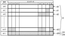
- FIG. 2 is a diagram showing an outline of data group D.
- the areas in which the bit data b0 to b15 are stored are shown hatched, and the areas in which the bit data b0 to b15 are not stored are shown as blank.
- FIG. 2 also shows the addresses adr0 to adrn in which the data d0 to d28 are stored, respectively.
- data group D is composed of data d0 to d27.
- Data d0 to d27 include parameter data necessary for the internal control of the internal control circuit 13 described below, or execution flags necessary for the internal processing executed by the internal control circuit 13, etc.
- Each of the data d0 to d28 is bit data of multiple bits (up to 16 bits in this case).
- Each of the data d0 to d28 may store all of the bit data b0 to b15, or may store any of the bit data b0 to b15.
- data d0 includes one 1-bit data (such as a flag of 0 or 1), as indicated by bit b0.
- Data d2 includes one 3-bit data (such as a parameter that can take eight values from 0 to 7), as indicated by bits b1 to b3.
- Data d27 includes one 1-bit data and two 2-bit data (such as a parameter that can take four values from 0 to 3), as indicated by bit b0, bits b2 to b3, and bits b14 to b15, respectively.
- Each of the data d0 to d28 is stored in the area specified by the storage address adr0 to adrn (more specifically, in one of the data storage areas 9 in register 6, which will be described later).
- the judgment data CRCW is calculated by a CRC (Cyclic Redundancy Check) calculation based on the normal data group D.
- the control circuit 2 calculates the judgment data CRCW in advance and then transmits the data group D and the judgment data CRCW to the semiconductor device 3.
- control circuit 2 can be configured to include a non-volatile memory 12. In this case, the control circuit 2 transmits the data group D stored in this non-volatile memory 12 to the semiconductor device 3.
- the semiconductor device 3 is an integrated circuit (IC) that integrates multiple elements.
- the semiconductor device 3 includes a receiving circuit 4, a receiving judgment circuit 5, a register 6, a register monitoring circuit 7, an internal control circuit 13, and a transmitting circuit 8.
- the receiving circuit 4 is a circuit that receives various data from the control circuit 2.
- the receiving circuit 4 can transmit the data group D and the judgment data CRCW received from the control circuit 2 to the register 6.
- the reception judgment circuit 5 is electrically connected to the receiving circuit 4.
- the reception judgment circuit 5 judges whether the data group D and judgment data CRCW received by the receiving circuit 4 are normal or not. More specifically, it judges whether data d0 to data d28 are normal values or not.
- the reception judgment circuit 5 transmits the result of this judgment (hereinafter referred to as the "judgment result S1") to the transmitting circuit 8, which will be described later. The judgment by the reception judgment circuit 5 will be described in detail later.
- the register 6 is electrically connected to the receiving circuit 4.
- the register 6 can store predetermined data. Specifically, the register 6 can store the data group D and the judgment data CRCW.
- the register monitoring circuit 7 is electrically connected to the register 6.
- the register monitoring circuit 7 monitors the register 6. Specifically, the register monitoring circuit 7 monitors the register 6 by periodically determining whether the data group D stored in the register 6 is normal or not (more specifically, whether the data d0 to data d27 stored in the register 6 are normal values or not).
- the register monitoring circuit 7 compares the check code CRCR with the judgment data CRCW and determines whether they match or not. If the check code CRCR and the judgment data CRCW match, the data group D is determined to be normal (more specifically, data d0 to data d27 are normal values). If the check code CRCR and the judgment data CRCW do not match, the data group D is determined to be abnormal (more specifically, at least one of data d0 to data d27 is not a normal value).
- the register monitoring circuit 7 transmits a judgment result S2 indicating whether the data group D is normal or not to the transmission circuit 8. If the judgment result S2 indicates that the data group D is normal, then after a predetermined time has elapsed since the transmission of the judgment result S2, the register monitoring circuit 7 again reads out the data group D stored in the register 6, calculates the check code CRCR, and judges whether the data group D is normal or not as described above. Thereafter, the calculation of the check code CRCR and the judgment of whether the data group D is normal or not are periodically performed. At this time, the register monitoring circuit 7 reads out the data group D stored in the register 6 each time and calculates the check code CRCR.
- the transmission circuit 8 receives the judgment result S1 and outputs the judgment result S1 to the outside (more specifically, the control circuit 2).
- the transmission circuit 8 also receives the judgment result S2 and outputs the judgment result S2 to the outside (more specifically, the control circuit 2).
- control circuit 2 When the control circuit 2 receives the judgment result S1 or S2 from the transmission circuit 8 indicating that the data group D is abnormal, it transmits the data group D to the semiconductor device 3 (more specifically, the receiving circuit 4).
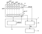
- FIG. 3 is a block diagram showing the register 6 and the register monitoring circuit 7. As shown in FIG. 3, the register 6 is composed of multiple (28 in this case) parameter storage areas 9, a judgment data storage area 10, and a code storage unit 11. Addresses adr0 to adr27 are assigned to each parameter storage area 9. Address adrn is assigned to the judgment data storage area 10.
- the data d0 to d27 are assigned and stored one by one in each parameter storage area 9.
- the check code CRCR is stored in the code storage unit 11.
- the receiving circuit 4 receives data d0 through d28 one by one in sequence from the control circuit 2.
- control circuit 2 When the control circuit 2 transmits data d0 to d28 to the semiconductor device 3 (more specifically, to the receiving circuit 4), it transmits the corresponding determination code together with the data d0 to d28. That is, when the control circuit 2 transmits data d0, it transmits the determination code corresponding to data d0 together with the data d0. When the control circuit 2 transmits data d1, it transmits the determination code corresponding to data d1 together with the data d1. The same applies to data d2 to data d28.
- the details of the judgment made by the reception judgment circuit 5 described above are as follows: When the reception circuit 4 receives one of the data d0 to d28, the reception judgment circuit 5 compares that one of the data d0 to d28 with the judgment code received along with it, and judges whether they match or not.
- the judgment result S1 is sent to the transmitting circuit 8 each time a judgment is made. If the judgment result S1 indicates that the data d0 to d28 received by the receiving circuit 4 are normal values, the control circuit 2 sends the subsequent data d1 to d28 to the receiving circuit 4.
- the reception judgment circuit 5 judges whether the data d0 is normal or not. If it is normal, the receiving circuit 4 stores the data d0 in a predetermined parameter storage area 9 (more specifically, the parameter storage area 9 corresponding to address adr0) (see Figure 3). Then, it receives data d1 from the control circuit 2. Similarly, the reception judgment circuit 5 judges whether the data d1 is normal or not, and if it is normal, the receiving circuit 4 stores the data d1 in the parameter storage area 9 (more specifically, the parameter storage area 9 corresponding to address adr1). Thereafter, it similarly receives data d2 to d28 and stores them in the parameter storage area 9 and the judgment data storage area 10.
- the control circuit 2 upon receiving the judgment result S1, suspends the transmission of the data d0 to d28 to the semiconductor device 3 at the point in time when it receives the judgment result S1.
- the control circuit 2 then retransmits the data d0 to d28 to the semiconductor device 3 in sequence, starting with the first data d0.
- the register monitoring circuit 7 includes a calculation circuit 14 and a register determination circuit 15.
- the calculation circuit 14 is a circuit that performs a CRC calculation based on the data d0 to d27 to generate a check code CRCR.
- the calculation circuit 14 stores the generated check code CRCR in the code storage unit 11.
- the register determination circuit 15 compares the check code CRCR stored in the code storage unit 11 with the determination data CRCW stored in the determination data storage area 10, determines whether the two match, and outputs the determination result S2 to the transmission circuit 8.
- FIG. 4 is a timing chart showing the operation of the semiconductor device 3. From the top, it shows the chip select signal CSB, the serial input signal SDI, the monitoring status of the register monitoring circuit 7 (CRC status), the error flag (Error REG), and the state of the semiconductor device 3 (IC status).
- the control circuit 2 starts writing data group D (data d0) to the register 6. Then, the chip select signal CSB falls to a low level. At this time, the state of the semiconductor device 3 is a standby state in which internal control has been stopped.
- the chip select signal CSB rises to a high level.
- judgment data CRCW is then stored in register 6. More specifically, data d28 is stored in judgment data storage area 10.
- the monitoring state of the register monitoring circuit 7 becomes the monitoring state (CRC calc). Specifically, at time t6, the register monitoring circuit 7 starts monitoring the register 6.
- the calculation circuit 14 acquires data d0 to d27 from each parameter storage area 9 and starts generating the check code CRCR. Then, by the time t7, the calculation circuit 14 stores the generated check code CRCR in the code storage unit 11, and the register judgment circuit 15 acquires and compares the check code CRCR with the judgment data CRCW, judges whether the judgment of the data group D is normal or not, and transmits the judgment result S2 to the transmission circuit 8.
- the check code CRCR and the judgment data CRCW match, and the data group D is judged to be normal (more specifically, the data d0 to d27 stored in register 6 are normal values).
- One judgment process (the process performed between time t6 and time t7) is completed in a few ⁇ S to a few tens of ⁇ S.
- semiconductor device 3 (more specifically, internal control circuit 13) starts internal control. Therefore, when time t7 arrives, the state of semiconductor device 3 becomes active state.
- the error flag (Error REG) rises to a high level. Also, when the error flag (Error REG) rises to a high level, the semiconductor device 3 again transitions to a standby state in which internal control is stopped.
- an error clear command ERCLR is sent from the control circuit 2, and data dx for executing error clear is stored in the parameter storage area 9.
- the chip select signal CSB falls from high to low.
- the error flag (Error REG) falls from high to low.
- the data dx can be one that is not included in the data group D described above (i.e. does not correspond to data d0 to d27).
- the monitoring state of the register monitoring circuit 7 becomes the monitoring state (CRC calc). Specifically, when time t13 arrives, the register monitoring circuit 7 starts monitoring the register 6. Then, when time t14 arrives and it is determined that the data group D is normal, the semiconductor device 3 starts internal control again and becomes active (not shown). Thereafter, the register monitoring circuit 7 continues monitoring the register 6.
- Register corruption is a phenomenon in which data in a register is unintentionally changed or corrupted.
- control circuit CPU, MCU, etc.
- a group of data is sent from the control circuit to the semiconductor device and stored in the register.
- Some of these semiconductor devices are configured to include a non-volatile memory inside the semiconductor device.
- the semiconductor device stores the data group written to the non-volatile memory in a register.
- the internal control circuit then reads out the data group stored in the register and performs the specified internal control.
- semiconductor devices that can read data groups from a non-volatile memory that is located outside the semiconductor device (for example, inside the control circuit) and store the data groups in a register.
- the control circuit stores the data groups from the non-volatile memory in the register.
- control circuit in a semiconductor device configured to store data groups in a register from an external non-volatile memory, the control circuit must periodically store the data groups in the register of the semiconductor device. This means that extra resources of the control circuit must be allocated to deal with register corruption, which is inefficient.
- the register monitoring circuit 7 is configured to periodically determine whether the data group D stored in the register 6 is normal or not. This eliminates the need to periodically re-store the data group D that is not necessarily abnormal, thereby shortening the time required to overwrite the register 6. This makes it possible to reduce the time required for internal control while suppressing the occurrence of malfunctions in the internal control.
- the calculation circuit 14 is able to calculate the check code CRCW based on the data group D stored in the register 6.
- the judgment data that the register judgment circuit 15 uses to compare with the check code CRCW is also stored in the register 6. Therefore, when judging whether the data group D in the register 6 is normal or not, there is no need to read out additional data from outside the semiconductor device 3 (here, the non-volatile memory 12), which simplifies the monitoring of the register 6. Therefore, the time required for the above-mentioned judgment can be shortened.
- control circuit 2 when determining whether the data group D in the register 6 is normal or not, the control circuit 2 does not need to store the data group D in the register 6. Therefore, there is no need to allocate the resources of the control circuit 2 to measures against register corruption.
- the register monitoring circuit 7 can determine whether the data group D is normal or not by a cyclic redundancy check using the check code CRCR calculated by the CRC calculation and the determination data CRCW. This makes it possible to more appropriately determine whether the data group D is normal or not compared to the case where other error detection methods are used.
- the register monitoring circuit 7 stops monitoring the register 6. While the data group D is in an abnormal state and a normal data group D is being written to the register 6 again, it is clear that the data group D stored in the register 6 is abnormal, so there is no need to monitor the register 6. For this reason, by temporarily stopping monitoring by the register monitoring circuit 7 during this time, the power consumption of the semiconductor device 3 can be reduced.
- the reception judgment circuit 5 is capable of judging whether the data group D received by the receiving circuit 12 is normal or not. If the judgment result S1 indicates that the data group D is not normal, the data group D is stored again in the register 6. This makes it possible to discover any defects in the data group D during reception when the data group D is stored in the register 6 from outside. Therefore, it is possible to re-store a normal data group D in the register 6 before a defect occurs in the internal control of the semiconductor device 3.
- the method of monitoring register 6 in the above embodiment is to calculate the check code CRCR by CRC calculation and determine whether data group D is normal or not, but this is not limited to this.
- the non-volatile memory 12 is included in the control circuit 2, but this is not limiting.
- the data group D and the judgment data CRCW are written from the control circuit 2 to this non-volatile memory.
- the data group D and the judgment data CRCW are stored from this non-volatile memory to the register 6.
- the register monitoring circuit 7 periodically monitors the register 6, eliminating the need to repeatedly read data from the non-volatile memory as in the conventional semiconductor device described above. As a result, the time required to take measures against data corruption in the register 6 is relatively short.
- the data group D can be composed of n-1 pieces of data, and the data related to the CRCW for validity determination can be the nth piece of data following the last piece of data in the data group D, as in the above embodiment.
- the data group D is incremented by one in order from data d0 to data d27, but this is not limited to this. In other words, it may not include any of the data d0 to d27.
- the semiconductor device (3) disclosed in the specification has a configuration (first configuration) including a register (6) capable of storing predetermined data, and a register monitoring circuit (7) configured to monitor the register (6) so as to periodically determine whether a data group (D) stored in the register (6) is normal or not.
- the semiconductor device (3) having the first configuration may be configured such that the data group (D) and judgment data (CRCW) based on the normal data group (D) are stored in the register (6), and the register monitoring circuit (7) compares the check code (CRCR) calculated from the data group (D) stored in the register (6) with the judgment data (CRCW) to determine whether the data group (D) stored in the register (6) is a normal value or not (second configuration).
- the register monitoring circuit (7) compares the check code (CRCR) calculated from the data group (D) stored in the register (6) with the judgment data (CRCW) to determine whether the data group (D) stored in the register (6) is a normal value or not (second configuration).
- the register monitoring circuit (7) may be configured to calculate the check code (CRCR) by CRC calculation (third configuration).
- the semiconductor device (3) having the third configuration may be configured such that the judgment data (CRCW) is a value calculated in advance by CRC calculation of the data group (D) based on the normal values of the configuration data (d0 to d27), and the register monitoring circuit (7) determines whether the judgment data (CRCW) and the check code (CRCR) match/mismatch to determine whether the data group (D) is normal or not (fourth configuration).
- the judgment data (CRCW) is a value calculated in advance by CRC calculation of the data group (D) based on the normal values of the configuration data (d0 to d27)
- the register monitoring circuit (7) determines whether the judgment data (CRCW) and the check code (CRCR) match/mismatch to determine whether the data group (D) is normal or not (fourth configuration).
- the semiconductor device (3) having the first configuration may be configured to include a transmission circuit (8) that transmits the judgment result (S2) of the data group (D) to the outside (fifth configuration).
- the register monitoring circuit (7) may be configured to stop monitoring the register (6) while the data group (D) is being written to the register (6) from outside, and to resume monitoring the register (6) after the writing of the data group (D) to the register (6) from outside is completed (sixth configuration).
- the semiconductor device (3) having the first configuration may also be configured to include a receiving circuit (4) that receives from the outside a data group (D) to be written to the register (6), and a receiving judgment circuit (5) that judges whether the data group (D) received by the receiving circuit (4) is normal or not (seventh configuration).
- the information processing device (1) disclosed in the specification has a configuration (8th configuration) including a semiconductor device (3) having any of the first to seventh configurations and a control circuit (2) configured to be able to write a data group (D) to a register (6).
- the information processing device (1) disclosed in the specification includes a semiconductor device (3) of the fifth or sixth configuration, and a control circuit (2) configured to be able to write data group (D) to a register (6), and the control circuit (2) is configured (ninth configuration) to write data group (D) to register (6) when a monitoring result indicates that data group (D) is abnormal.
- the semiconductor device (3) of the first configuration can periodically determine whether the data group (D) stored in the register (6) is normal. This eliminates the need to periodically re-store the data group (D), and shortens the time required to overwrite the register (6). This makes it possible to monitor the register (6) in a relatively short read time, thereby preventing malfunctions in the internal control.
- the semiconductor device (3) of the second configuration makes it possible to calculate the check code (CRCR) based on the data group (D) stored in the register (6).
- the judgment data (CRCW) used for comparison with the check code (CRCR) is also stored in the register (6). Therefore, when judging whether the data group (D) in the register (6) is normal or not, there is no need to read out additional data from outside the semiconductor device (3), and monitoring of the register (6) becomes easier. Therefore, the time required for the above-mentioned judgment can be shortened.
- the semiconductor device (3) of the third configuration makes it possible to more efficiently calculate the check code (CRCR), and efficiently determine whether the data group (D) is normal or not.
- the semiconductor device (3) of the fourth configuration makes it possible to more efficiently calculate the check code (CRCR) and the determination data (CRCW), and can more efficiently determine whether the data group (D) is normal or not.
- the semiconductor device (3) according to the fifth configuration makes it possible to configure a system capable of various controls using the judgment result (S2) output to the outside.
- the semiconductor device (3) of the seventh configuration makes it possible to discover defects in the data group (D) during reception when the data group (D) is stored in the register (6) from outside. This makes it possible to re-store a normal data group (D) in the register (6) before a defect occurs in the internal control of the semiconductor device (3).
- the information processing device (1) according to the eighth configuration can provide an information processing device (1) capable of monitoring the register (6) in a relatively short read time and preventing malfunctions from occurring in the internal control of the semiconductor device (3).
Landscapes
- Engineering & Computer Science (AREA)
- Theoretical Computer Science (AREA)
- General Engineering & Computer Science (AREA)
- Quality & Reliability (AREA)
- Physics & Mathematics (AREA)
- General Physics & Mathematics (AREA)
- Computer Hardware Design (AREA)
- Detection And Correction Of Errors (AREA)
Abstract
Description
ここで、いわゆるレジスタ化け対策に関して考察する。レジスタ化けとは、レジスタ内のデータが意図せず変更されたり、破損したりする現象である。
対して、本開示に係る上記実施形態の半導体装置3は、上述した通り、レジスタ監視回路7が、レジスタ6に格納されたデータ群Dが正常であるか否か定期的に判定するように構成されている。これにより、必ずしも異常が生じていないデータ群Dを定期的に格納し直す必要がなくなり、レジスタ6の上書きに必要な時間を短縮できる。このため、内部制御に要する時間を短くしつつ、内部制御に不具合が発生するのを抑制できるようになる。
2 制御回路
3 半導体装置
4 受信回路
5 受信判定回路
6 レジスタ
7 レジスタ監視回路
8 送信回路
9 パラメータ格納領域
10 判定用データ格納領域
11 符号格納部
12 不揮発性メモリ
13 内部制御回路
14 計算回路
15 レジスタ判定回路
adr0~adr27、adrn アドレス
CRCW 判定結果
CRCR 検査符号
CSB チップセレクト信号
d0~d28、dx データ
D データ群
S1、S2 判定結果
SDI シリアル入力信号
t1~t14 時刻
Claims (9)
- 所定のデータを格納可能なレジスタと、
前記レジスタに格納されたデータ群が正常であるか否かを定期的に判定するように前記レジスタを監視するよう構成されたレジスタ監視回路と、
を備える半導体装置。 - 正常な前記データ群に基づく判定用データと、前記データ群とが前記レジスタに格納され、
前記レジスタ監視回路は、前記レジスタに格納された前記データ群から算出した検査符号と、前記判定用データとを比較して、前記レジスタに格納された前記データ群が正常であるか否かを判定する請求項1に記載の半導体装置。 - 前記レジスタ監視回路は、CRC演算によって前記検査符号を算出する請求項2に記載の半導体装置。
- 前記判定用データは、前記データ群を構成する各データの正常値に基づいてCRC演算によって予め算出された値であり、
前記レジスタ監視回路は、前記判定用データと前記検査符号との一致/不一致を判定することで、前記データ群が正常であるか否かを判定する請求項3に記載の半導体装置。 - 前記データ群の判定結果を外部に送信する送信回路を備える請求項1に記載の半導体装置。
- 前記レジスタ監視回路は、前記データ群が前記外部から前記レジスタに書き込まれている間に、前記レジスタの監視を停止し、前記外部から前記データ群の前記レジスタへの書き込みが完了した後に前記レジスタの監視を再開する請求項5に記載の半導体装置。
- 前記レジスタへの書き込み対象である前記データ群を外部から受信する受信回路と、
前記受信回路が受信した前記データ群が正常であるか否か判定する受信判定回路と、
を備える請求項1に記載の半導体装置。 - 請求項1から7のいずれかに記載の半導体装置と、
前記レジスタに前記データ群を書き込み可能なように構成された制御回路と、
を備える情報処理装置。 - 請求項5または6に記載の半導体装置と、
前記レジスタに前記データ群を書き込み可能なように構成された制御回路と、
を備え、
前記制御回路は、前記データ群が正常ではないとする前記監視結果を受けた場合に、前記データ群を前記レジスタに書き込む情報処理装置。
Priority Applications (1)
| Application Number | Priority Date | Filing Date | Title |
|---|---|---|---|
| JP2025506675A JPWO2024190403A1 (ja) | 2023-03-16 | 2024-02-27 |
Applications Claiming Priority (2)
| Application Number | Priority Date | Filing Date | Title |
|---|---|---|---|
| JP2023-041635 | 2023-03-16 | ||
| JP2023041635 | 2023-03-16 |
Publications (1)
| Publication Number | Publication Date |
|---|---|
| WO2024190403A1 true WO2024190403A1 (ja) | 2024-09-19 |
Family
ID=92754961
Family Applications (1)
| Application Number | Title | Priority Date | Filing Date |
|---|---|---|---|
| PCT/JP2024/007100 Ceased WO2024190403A1 (ja) | 2023-03-16 | 2024-02-27 | 半導体装置、およびそれを備えた情報処理装置 |
Country Status (2)
| Country | Link |
|---|---|
| JP (1) | JPWO2024190403A1 (ja) |
| WO (1) | WO2024190403A1 (ja) |
Citations (2)
| Publication number | Priority date | Publication date | Assignee | Title |
|---|---|---|---|---|
| JP2005234883A (ja) * | 2004-02-19 | 2005-09-02 | Nec Corp | 記憶装置のデータ書き込み、読み出し方法およびデータ記憶システム |
| US20170031750A1 (en) * | 2015-07-28 | 2017-02-02 | Microchip Technology Incorporated | Zero Overhead Code Coverage Analysis |
-
2024
- 2024-02-27 JP JP2025506675A patent/JPWO2024190403A1/ja active Pending
- 2024-02-27 WO PCT/JP2024/007100 patent/WO2024190403A1/ja not_active Ceased
Patent Citations (2)
| Publication number | Priority date | Publication date | Assignee | Title |
|---|---|---|---|---|
| JP2005234883A (ja) * | 2004-02-19 | 2005-09-02 | Nec Corp | 記憶装置のデータ書き込み、読み出し方法およびデータ記憶システム |
| US20170031750A1 (en) * | 2015-07-28 | 2017-02-02 | Microchip Technology Incorporated | Zero Overhead Code Coverage Analysis |
Also Published As
| Publication number | Publication date |
|---|---|
| JPWO2024190403A1 (ja) | 2024-09-19 |
Similar Documents
| Publication | Publication Date | Title |
|---|---|---|
| KR101374455B1 (ko) | 메모리 에러와 리던던시 | |
| US8566672B2 (en) | Selective checkbit modification for error correction | |
| US20120079346A1 (en) | Simulated error causing apparatus | |
| JP6841698B2 (ja) | 半導体装置 | |
| US20080126905A1 (en) | Memory control device, computer system and data reproducing and recording device | |
| EP2770507A2 (en) | Memory circuits, method for accessing a memory and method for repairing a memory | |
| US20130305000A1 (en) | Signal processing circuit | |
| CN111880961A (zh) | 用于透明寄存器数据错误检测和纠正的系统和方法 | |
| JP2008262325A (ja) | メモリ制御装置、メモリ制御方法、情報処理システム、そのプログラム及び記憶媒体 | |
| JP4373615B2 (ja) | 初期不良ブロックのマーキング方法 | |
| US8291270B2 (en) | Request processing device, request processing system, and access testing method | |
| WO2024190403A1 (ja) | 半導体装置、およびそれを備えた情報処理装置 | |
| US11831337B2 (en) | Semiconductor device and error detection methods | |
| US11630600B2 (en) | Device and method for checking register data | |
| CN117524290A (zh) | 一种片上存储纠错系统 | |
| JP6193112B2 (ja) | メモリアクセス制御装置、メモリアクセス制御システム、メモリアクセス制御方法、及び、メモリアクセス制御プログラム | |
| JP7350488B2 (ja) | 周辺装置制御システム、および周辺装置制御方法 | |
| EP3882774A1 (en) | Data processing device and data processing method | |
| US7484147B2 (en) | Semiconductor integrated circuit | |
| EP3404547B1 (en) | Method for supervising and initializing ports | |
| KR20220144129A (ko) | 메모리 장치 및 그것을 포함하는 반도체 시스템 | |
| KR102868477B1 (ko) | 반도체 칩 내부 sram의 불량 셀 검사 방법 및 그 방법으로 동작하는 장치 | |
| US10963344B2 (en) | Information processing circuitry, information processing method, and non-transitory computer readable medium | |
| JP4985462B2 (ja) | 集積回路、集積回路の動作試験方法および動作試験プログラム | |
| JP2001167002A (ja) | 電子ディスク装置の書き込み/読み出し制御方法及びその装置 |
Legal Events
| Date | Code | Title | Description |
|---|---|---|---|
| 121 | Ep: the epo has been informed by wipo that ep was designated in this application |
Ref document number: 24770515 Country of ref document: EP Kind code of ref document: A1 |
|
| ENP | Entry into the national phase |
Ref document number: 2025506675 Country of ref document: JP Kind code of ref document: A |
|
| WWE | Wipo information: entry into national phase |
Ref document number: 2025506675 Country of ref document: JP |
|
| NENP | Non-entry into the national phase |
Ref country code: DE |
|
| 122 | Ep: pct application non-entry in european phase |
Ref document number: 24770515 Country of ref document: EP Kind code of ref document: A1 |