WO2024185313A1 - 半導体装置および半導体装置の製造方法 - Google Patents
半導体装置および半導体装置の製造方法 Download PDFInfo
- Publication number
- WO2024185313A1 WO2024185313A1 PCT/JP2024/001519 JP2024001519W WO2024185313A1 WO 2024185313 A1 WO2024185313 A1 WO 2024185313A1 JP 2024001519 W JP2024001519 W JP 2024001519W WO 2024185313 A1 WO2024185313 A1 WO 2024185313A1
- Authority
- WO
- WIPO (PCT)
- Prior art keywords
- region
- trench
- doping concentration
- semiconductor substrate
- semiconductor device
- Prior art date
- Legal status (The legal status is an assumption and is not a legal conclusion. Google has not performed a legal analysis and makes no representation as to the accuracy of the status listed.)
- Ceased
Links
Images




Classifications
-
- H—ELECTRICITY
- H10—SEMICONDUCTOR DEVICES; ELECTRIC SOLID-STATE DEVICES NOT OTHERWISE PROVIDED FOR
- H10P—GENERIC PROCESSES OR APPARATUS FOR THE MANUFACTURE OR TREATMENT OF DEVICES COVERED BY CLASS H10
- H10P30/00—Ion implantation into wafers, substrates or parts of devices
- H10P30/20—Ion implantation into wafers, substrates or parts of devices into semiconductor materials, e.g. for doping
- H10P30/222—Ion implantation into wafers, substrates or parts of devices into semiconductor materials, e.g. for doping characterised by the angle between the ion beam and the crystal planes or the main crystal surface
-
- H—ELECTRICITY
- H10—SEMICONDUCTOR DEVICES; ELECTRIC SOLID-STATE DEVICES NOT OTHERWISE PROVIDED FOR
- H10D—INORGANIC ELECTRIC SEMICONDUCTOR DEVICES
- H10D12/00—Bipolar devices controlled by the field effect, e.g. insulated-gate bipolar transistors [IGBT]
- H10D12/01—Manufacture or treatment
- H10D12/031—Manufacture or treatment of IGBTs
- H10D12/032—Manufacture or treatment of IGBTs of vertical IGBTs
- H10D12/038—Manufacture or treatment of IGBTs of vertical IGBTs having a recessed gate, e.g. trench-gate IGBTs
-
- H—ELECTRICITY
- H10—SEMICONDUCTOR DEVICES; ELECTRIC SOLID-STATE DEVICES NOT OTHERWISE PROVIDED FOR
- H10D—INORGANIC ELECTRIC SEMICONDUCTOR DEVICES
- H10D12/00—Bipolar devices controlled by the field effect, e.g. insulated-gate bipolar transistors [IGBT]
- H10D12/411—Insulated-gate bipolar transistors [IGBT]
- H10D12/441—Vertical IGBTs
- H10D12/461—Vertical IGBTs having non-planar surfaces, e.g. having trenches, recesses or pillars in the surfaces of the emitter, base or collector regions
- H10D12/481—Vertical IGBTs having non-planar surfaces, e.g. having trenches, recesses or pillars in the surfaces of the emitter, base or collector regions having gate structures on slanted surfaces, on vertical surfaces, or in grooves, e.g. trench gate IGBTs
-
- H—ELECTRICITY
- H10—SEMICONDUCTOR DEVICES; ELECTRIC SOLID-STATE DEVICES NOT OTHERWISE PROVIDED FOR
- H10D—INORGANIC ELECTRIC SEMICONDUCTOR DEVICES
- H10D30/00—Field-effect transistors [FET]
- H10D30/01—Manufacture or treatment
- H10D30/021—Manufacture or treatment of FETs having insulated gates [IGFET]
-
- H—ELECTRICITY
- H10—SEMICONDUCTOR DEVICES; ELECTRIC SOLID-STATE DEVICES NOT OTHERWISE PROVIDED FOR
- H10D—INORGANIC ELECTRIC SEMICONDUCTOR DEVICES
- H10D30/00—Field-effect transistors [FET]
- H10D30/60—Insulated-gate field-effect transistors [IGFET]
-
- H—ELECTRICITY
- H10—SEMICONDUCTOR DEVICES; ELECTRIC SOLID-STATE DEVICES NOT OTHERWISE PROVIDED FOR
- H10D—INORGANIC ELECTRIC SEMICONDUCTOR DEVICES
- H10D62/00—Semiconductor bodies, or regions thereof, of devices having potential barriers
- H10D62/10—Shapes, relative sizes or dispositions of the regions of the semiconductor bodies; Shapes of the semiconductor bodies
- H10D62/102—Constructional design considerations for preventing surface leakage or controlling electric field concentration
- H10D62/103—Constructional design considerations for preventing surface leakage or controlling electric field concentration for increasing or controlling the breakdown voltage of reverse-biased devices
- H10D62/105—Constructional design considerations for preventing surface leakage or controlling electric field concentration for increasing or controlling the breakdown voltage of reverse-biased devices by having particular doping profiles, shapes or arrangements of PN junctions; by having supplementary regions, e.g. junction termination extension [JTE]
- H10D62/106—Constructional design considerations for preventing surface leakage or controlling electric field concentration for increasing or controlling the breakdown voltage of reverse-biased devices by having particular doping profiles, shapes or arrangements of PN junctions; by having supplementary regions, e.g. junction termination extension [JTE] having supplementary regions doped oppositely to or in rectifying contact with regions of the semiconductor bodies, e.g. guard rings with PN or Schottky junctions
- H10D62/107—Buried supplementary regions, e.g. buried guard rings
-
- H—ELECTRICITY
- H10—SEMICONDUCTOR DEVICES; ELECTRIC SOLID-STATE DEVICES NOT OTHERWISE PROVIDED FOR
- H10D—INORGANIC ELECTRIC SEMICONDUCTOR DEVICES
- H10D64/00—Electrodes of devices having potential barriers
- H10D64/111—Field plates
- H10D64/117—Recessed field plates, e.g. trench field plates or buried field plates
-
- H—ELECTRICITY
- H10—SEMICONDUCTOR DEVICES; ELECTRIC SOLID-STATE DEVICES NOT OTHERWISE PROVIDED FOR
- H10D—INORGANIC ELECTRIC SEMICONDUCTOR DEVICES
- H10D8/00—Diodes
-
- H—ELECTRICITY
- H10—SEMICONDUCTOR DEVICES; ELECTRIC SOLID-STATE DEVICES NOT OTHERWISE PROVIDED FOR
- H10D—INORGANIC ELECTRIC SEMICONDUCTOR DEVICES
- H10D8/00—Diodes
- H10D8/422—PN diodes having the PN junctions in mesas
-
- H—ELECTRICITY
- H10—SEMICONDUCTOR DEVICES; ELECTRIC SOLID-STATE DEVICES NOT OTHERWISE PROVIDED FOR
- H10D—INORGANIC ELECTRIC SEMICONDUCTOR DEVICES
- H10D8/00—Diodes
- H10D8/50—PIN diodes
-
- H—ELECTRICITY
- H10—SEMICONDUCTOR DEVICES; ELECTRIC SOLID-STATE DEVICES NOT OTHERWISE PROVIDED FOR
- H10D—INORGANIC ELECTRIC SEMICONDUCTOR DEVICES
- H10D84/00—Integrated devices formed in or on semiconductor substrates that comprise only semiconducting layers, e.g. on Si wafers or on GaAs-on-Si wafers
- H10D84/01—Manufacture or treatment
- H10D84/0107—Integrating at least one component covered by H10D12/00 or H10D30/00 with at least one component covered by H10D8/00, H10D10/00 or H10D18/00, e.g. integrating IGFETs with BJTs
- H10D84/0109—Integrating at least one component covered by H10D12/00 or H10D30/00 with at least one component covered by H10D8/00, H10D10/00 or H10D18/00, e.g. integrating IGFETs with BJTs the at least one component covered by H10D12/00 or H10D30/00 being a MOS device
-
- H—ELECTRICITY
- H10—SEMICONDUCTOR DEVICES; ELECTRIC SOLID-STATE DEVICES NOT OTHERWISE PROVIDED FOR
- H10D—INORGANIC ELECTRIC SEMICONDUCTOR DEVICES
- H10D84/00—Integrated devices formed in or on semiconductor substrates that comprise only semiconducting layers, e.g. on Si wafers or on GaAs-on-Si wafers
- H10D84/101—Integrated devices comprising main components and built-in components, e.g. IGBT having built-in freewheel diode
- H10D84/161—IGBT having built-in components
-
- H—ELECTRICITY
- H10—SEMICONDUCTOR DEVICES; ELECTRIC SOLID-STATE DEVICES NOT OTHERWISE PROVIDED FOR
- H10D—INORGANIC ELECTRIC SEMICONDUCTOR DEVICES
- H10D84/00—Integrated devices formed in or on semiconductor substrates that comprise only semiconducting layers, e.g. on Si wafers or on GaAs-on-Si wafers
- H10D84/80—Integrated devices formed in or on semiconductor substrates that comprise only semiconducting layers, e.g. on Si wafers or on GaAs-on-Si wafers characterised by the integration of at least one component covered by groups H10D12/00 or H10D30/00, e.g. integration of IGFETs
- H10D84/811—Combinations of field-effect devices and one or more diodes, capacitors or resistors
-
- H—ELECTRICITY
- H10—SEMICONDUCTOR DEVICES; ELECTRIC SOLID-STATE DEVICES NOT OTHERWISE PROVIDED FOR
- H10D—INORGANIC ELECTRIC SEMICONDUCTOR DEVICES
- H10D12/00—Bipolar devices controlled by the field effect, e.g. insulated-gate bipolar transistors [IGBT]
- H10D12/411—Insulated-gate bipolar transistors [IGBT]
- H10D12/418—Insulated-gate bipolar transistors [IGBT] having a drift region having a doping concentration that is higher at the emitter side relative to other parts of the drift region
-
- H—ELECTRICITY
- H10—SEMICONDUCTOR DEVICES; ELECTRIC SOLID-STATE DEVICES NOT OTHERWISE PROVIDED FOR
- H10D—INORGANIC ELECTRIC SEMICONDUCTOR DEVICES
- H10D62/00—Semiconductor bodies, or regions thereof, of devices having potential barriers
- H10D62/10—Shapes, relative sizes or dispositions of the regions of the semiconductor bodies; Shapes of the semiconductor bodies
- H10D62/124—Shapes, relative sizes or dispositions of the regions of semiconductor bodies or of junctions between the regions
- H10D62/126—Top-view geometrical layouts of the regions or the junctions
- H10D62/127—Top-view geometrical layouts of the regions or the junctions of cellular field-effect devices, e.g. multicellular DMOS transistors or IGBTs
Definitions
- the present invention relates to a semiconductor device and a method for manufacturing a semiconductor device.
- Patent Document 1 describes that "the semiconductor device may further include an electrically floating barrier region 105 of a second conductivity type (hereinafter also simply referred to as a 'barrier region')."
- Patent Documents [Patent Documents] [Patent Document 1] JP 2019-91892 A [Patent Document 2] Japanese Patent No. 6472714 A [Patent Document 3] Japanese Patent No. 5707681 A
- a semiconductor device having a transistor portion and a diode portion comprising: a plurality of trench portions including a gate trench portion provided on the front surface of a semiconductor substrate; a drift region of a first conductivity type provided in the semiconductor substrate; a base region of a second conductivity type provided above the drift region; an emitter region of the first conductivity type provided above the base region and having a doping concentration higher than that of the drift region; a first accumulation region of the first conductivity type provided below the base region and having a doping concentration higher than that of the drift region; a trench bottom region of a second conductivity type provided below the first accumulation region and having a doping concentration higher than that of the base region; and a second accumulation region of the first conductivity type provided deeper than the trench bottom region in the depth direction of the semiconductor substrate and having a doping concentration higher than that of the drift region.
- the upper end of the trench bottom region may be in contact with the lower end of the first accumulation region.
- the lower end of the trench bottom region may be in contact with the upper end of the second accumulation region.
- the trench bottom region may extend from a lower end of one of the plurality of trench portions to a lower end of the other opposing trench portion in the trench arrangement direction of the plurality of trench portions.
- the thickness of the trench bottom region in the depth direction of the semiconductor substrate may be 20% or more and 100% or less of the trench depth of the multiple trench portions.
- the thickness of the trench bottom region in the depth direction of the semiconductor substrate may be 1 ⁇ m or more and 5 ⁇ m or less.
- the trench bottom region includes a first region provided below the plurality of trench portions and a second region provided below a mesa portion sandwiched between the plurality of trench portions, and the doping concentration of the first region may be higher than the doping concentration of the second region.
- the trench bottom region includes a first region provided below the multiple trench portions and a second region provided below a mesa portion sandwiched between the multiple trench portions, and the doping concentration of the first region may be the same as the doping concentration of the second region.
- any of the above semiconductor devices may include a first conductivity type carrier passage region below the first accumulation region, in which the trench bottom region is not provided.
- the second accumulation region may have a protruding portion that extends from below the trench bottom region, beyond the end of the trench bottom region, and outside the trench bottom region in the trench arrangement direction of the multiple trench portions.
- the doping concentration in the first accumulation region may have a profile in which a region having a doping concentration of 50% or more of the maximum doping concentration in the first accumulation region occupies 60% or more and 100% or less of the thickness of the first accumulation region in the depth direction of the semiconductor substrate.
- the doping concentration in the first accumulation region may have one or more doping concentration peaks in the depth direction of the semiconductor substrate.
- the thickness of the region having a doping concentration of 50% or more of the maximum doping concentration in the first accumulation region in the depth direction of the semiconductor substrate may be 1 ⁇ m or more and 4 ⁇ m or less.
- a method for manufacturing a semiconductor device having a drift region of a first conductivity type includes the steps of forming a plurality of trenches on the front surface of a semiconductor substrate, forming a base region of a second conductivity type above the drift region, forming an emitter region of a first conductivity type above the base region and having a doping concentration higher than that of the drift region, forming a first accumulation region of a first conductivity type having a doping concentration higher than that of the drift region by ion implanting dopants from the front surface side of the semiconductor substrate, forming a trench bottom region of a second conductivity type having a doping concentration higher than that of the base region below the first accumulation region by ion implanting dopants from the front surface side of the semiconductor substrate, and forming a second accumulation region of a first conductivity type having a doping concentration higher than that of the drift region at a position deeper in the depth direction of the semiconductor substrate than the trench bottom region by ion implanting do
- the step of forming the first accumulation region may include the step of injecting dopants into the side walls of the plurality of trench portions through the openings of the plurality of trench portions from a direction having a predetermined inclination with respect to the depth direction of the semiconductor substrate.
- the step of forming the trench bottom region may include the step of injecting a dopant into the bottoms of the plurality of trench portions through the openings of the plurality of trench portions in the depth direction of the semiconductor substrate.
- the step of forming the second accumulation region may include the step of injecting dopants into the bottoms of the plurality of trench portions through the openings of the plurality of trench portions from a direction having a predetermined inclination with respect to the depth direction of the semiconductor substrate.
- any of the above methods for manufacturing a semiconductor device may include a step of forming the first accumulation region and an ion implantation step of forming the second accumulation region, and the ion implantation step may include a step of forming the first accumulation region by injecting a dopant into the sidewalls of the plurality of trench portions through the openings of the plurality of trench portions, and forming the second accumulation region by injecting the dopant into the bottoms of the plurality of trench portions through the openings of the plurality of trench portions.
- the steps of forming the second accumulation region, forming the trench bottom region, and forming the first accumulation region may be performed before the step of forming the multiple trench portions.
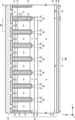
- FIG. 2 is a diagram showing an example of a top view of the semiconductor device 100.
- FIG. 1 is a diagram showing an example of a cross section of a semiconductor device 100.
- FIG. 1 shows an example of a doping concentration profile including a flat region.
- 1 is a diagram showing a modified example of the cross section of the semiconductor device 100.
- FIG. 1 is a diagram showing a modified example of the cross section of the semiconductor device 100.
- FIG. 1 is a diagram showing a modified example of the cross section of the semiconductor device 100.
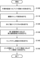
- FIG. 3 is a flowchart showing an example of a manufacturing process of the semiconductor device 100.
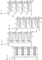
- 1A to 1C are diagrams illustrating an example of a manufacturing process for the semiconductor device 100.
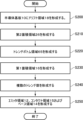
- 10 is a flowchart showing a modified example of the manufacturing process of the semiconductor device 100.
- 10A to 10C are diagrams illustrating a modified example of the manufacturing process of the semiconductor device 100.
- top one side in a direction parallel to the depth direction of the semiconductor substrate is referred to as "top” and the other side as “bottom.”
- bottom one surface is referred to as the top surface and the other surface is referred to as the bottom surface.
- the directions of "top,” “bottom,” “front,” and “back” are not limited to the direction of gravity or the direction in which the semiconductor device is attached to a substrate or the like when mounted.
- the orthogonal coordinate axes merely identify the relative positions of components, and do not limit a specific direction.
- the Z-axis does not limit the height direction relative to the ground.
- the +Z-axis direction and the -Z-axis direction are opposite directions.
- the Z-axis direction is described without indicating positive or negative, it means the direction parallel to the +Z-axis and -Z-axis.
- the plane parallel to the top surface of the semiconductor substrate is referred to as the XY plane, and the orthogonal axes parallel to the top and bottom surfaces of the semiconductor substrate are referred to as the X-axis and Y-axis.
- the axis perpendicular to the top and bottom surfaces of the semiconductor substrate is referred to as the Z-axis.
- the depth direction of the semiconductor substrate may be referred to as the Z-axis.
- the case where the semiconductor substrate is viewed in the Z-axis direction is referred to as a planar view.
- the direction parallel to the top and bottom surfaces of the semiconductor substrate, including the X-axis and Y-axis may be referred to as the horizontal direction.
- the first conductivity type is N-type and the second conductivity type is P-type, but the first conductivity type may be P-type and the second conductivity type may be N-type.
- the conductivity types of the substrate, layer, region, etc. in each embodiment will be of opposite polarity.
- the conductivity type of a doped region doped with impurities is described as P type or N type.
- impurities may particularly mean either N type donors or P type acceptors, and may be described as dopants.
- doping means introducing donors or acceptors into a semiconductor substrate to make it a semiconductor that exhibits N type conductivity or P type conductivity.
- doping concentration refers to the donor concentration or acceptor concentration in thermal equilibrium.
- FIG. 1 is a diagram showing an example of a top view of the semiconductor device 100 of this example.
- the semiconductor device 100 of this example is a semiconductor chip including a transistor section 70 and a diode section 80.
- the semiconductor device 100 is a reverse conducting IGBT (RC-IGBT).
- the transistor section 70 of this example includes a boundary section 90 in a portion adjacent to the diode section 80.
- the transistor section 70 is a region in which the collector region 22 provided on the back side of the semiconductor substrate 10 is projected onto the upper surface of the semiconductor substrate 10.
- the collector region 22 has a second conductivity type.
- the collector region 22 is a P+ type.
- the transistor section 70 includes a transistor such as an IGBT.
- the diode section 80 is a region obtained by projecting a cathode region 82 provided on the back surface of the semiconductor substrate 10 onto the upper surface of the semiconductor substrate 10.
- the cathode region 82 has a first conductivity type.
- the cathode region 82 is an N+ type, for example.
- the diode section 80 includes a diode such as a free wheel diode (FWD) provided adjacent to the transistor section 70 on the upper surface of the semiconductor substrate 10.
- FWD free wheel diode
- the boundary between the collector region 22 and the cathode region 82 is the boundary between the transistor section 70 and the diode section 80. That is, the collector region 22 is provided below the boundary section 90 in this example.
- An edge termination structure may be provided in the area on the negative side in the Y-axis direction of the semiconductor device 100 in this example.
- the edge termination structure relieves electric field concentration on the upper surface side of the semiconductor substrate 10.
- the edge termination structure has, for example, a guard ring, a field plate, a resurf, or a structure combining these. Note that in this example, for convenience, the edge on the negative side in the Y-axis direction is described, but the same applies to the other edges of the semiconductor device 100.
- the edge termination structure may be provided to surround an active region including a transistor portion 70 and a diode portion 80.
- the semiconductor substrate 10 may be a silicon substrate, a silicon carbide substrate, a nitride semiconductor substrate such as gallium nitride, etc.
- the semiconductor substrate 10 in this example is a silicon substrate.
- the semiconductor device 100 of this example includes a gate trench portion 40, a dummy trench portion 30, an emitter region 12, a base region 14, a contact region 15, a well region 17, and an anode region 19 on the front surface 21 of the semiconductor substrate 10.
- the front surface 21 will be described later.
- the semiconductor device 100 of this example also includes an emitter electrode 52 and a gate metal layer 50 provided above the front surface 21 of the semiconductor substrate 10.
- the emitter electrode 52 is provided above the gate trench portion 40, the dummy trench portion 30, the emitter region 12, the base region 14, the contact region 15, the well region 17, and the anode region 19.
- the gate metal layer 50 is provided above the connection portion 25 and the well region 17.
- the emitter electrode 52 and the gate metal layer 50 are formed of a material containing a metal. At least a portion of the emitter electrode 52 may be formed of a metal such as aluminum (Al) or a metal alloy such as aluminum-silicon alloy (AlSi) or aluminum-silicon-copper alloy (AlSiCu). At least a portion of the gate metal layer 50 may be formed of a metal such as aluminum (Al) or a metal alloy such as aluminum-silicon alloy (AlSi) or aluminum-silicon-copper alloy (AlSiCu). The emitter electrode 52 and the gate metal layer 50 may have a barrier metal layer made of titanium or a titanium compound under the region made of aluminum or the like. The emitter electrode 52 and the gate metal layer 50 are provided separately from each other.
- the emitter electrode 52 and the gate metal layer 50 are provided above the semiconductor substrate 10 with the interlayer insulating film 38 in between.
- the interlayer insulating film 38 is omitted in FIG. 1.
- the interlayer insulating film 38 has contact holes 54, 55, and 56 penetrating therethrough.
- the contact hole 55 electrically connects the gate metal layer 50 and the gate conductive portion in the transistor portion 70 via the connection portion 25.
- a plug layer made of tungsten or the like may be formed inside the contact hole 55.
- the contact hole 56 connects the emitter electrode 52 to the dummy conductive portion in the dummy trench portion 30.
- a plug layer made of tungsten or the like may be formed inside the contact hole 56.
- connection portion 25 is connected to the emitter electrode 52 or the front surface side metal layer such as the gate metal layer 50.
- the connection portion 25 is provided between the gate metal layer 50 and the gate conductive portion.
- the connection portion 25 in this example is provided extending in the X-axis direction and may be electrically connected to the gate conductive portion.
- the connection portion 25 may also be provided between the emitter electrode 52 and the dummy conductive portion.
- the connection portion 25 is a conductive material such as polysilicon doped with impurities.
- the connection portion 25 in this example is polysilicon (N+) doped with N-type impurities.
- the connection portion 25 is provided above the front surface 21 of the semiconductor substrate 10 via an insulating film such as an oxide film.
- the gate trench portion 40 is an example of a plurality of trench portions extending in a predetermined extension direction on the front surface 21 side of the semiconductor substrate 10.
- the gate trench portions 40 are arranged at predetermined intervals along a predetermined arrangement direction (the X-axis direction in this example).
- the gate trench portion 40 in this example may have two extension portions 41 extending parallel to the front surface 21 of the semiconductor substrate 10 and along an extension direction perpendicular to the arrangement direction (the Y-axis direction in this example), and a connection portion 43 connecting the two extension portions 41.
- connection portion 43 is formed in a curved shape.
- the gate metal layer 50 may be electrically connected to the gate conductive portion via the connection portion 25.
- the dummy trench portion 30 is an example of a plurality of trench portions extending in a predetermined extension direction on the front surface 21 side of the semiconductor substrate 10.
- the dummy trench portion 30 is a trench portion electrically connected to the emitter electrode 52.
- the dummy trench portion 30 is arranged at predetermined intervals along a predetermined arrangement direction (the X-axis direction in this example).
- the dummy trench portion 30 in this example has an I-shape on the front surface 21 of the semiconductor substrate 10.
- the dummy trench portion 30 may have a U-shape on the front surface 21 of the semiconductor substrate 10. That is, the dummy trench portion 30 may have two extension portions 31 extending along the extension direction and a connection portion 33 connecting the two extension portions.
- the transistor section 70 in this example has a structure in which two gate trench sections 40 and two dummy trench sections 30 are arranged in a repeated manner. That is, the transistor section 70 in this example has gate trench sections 40 and dummy trench sections 30 in a 1:1 ratio. For example, the transistor section 70 has one dummy trench section 30 between two extension sections 41.
- the ratio of the gate trench portion 40 to the dummy trench portion 30 is not limited to this example.
- the ratio of the gate trench portion 40 may be greater than the ratio of the dummy trench portion 30, and the ratio of the dummy trench portion 30 may be greater than the ratio of the gate trench portion 40.
- the ratio of the gate trench portion 40 to the dummy trench portion 30 may be 2:3 or 2:4.
- the transistor portion 70 may not have dummy trench portions 30, with all trench portions being gate trench portions 40.
- the well region 17 is a second conductivity type region provided on the front surface 21 side of the semiconductor substrate 10 relative to the drift region 18 described later.
- the well region 17 is an example of a well region provided on the peripheral side of the active region.
- the well region 17 is P+ type as an example.
- the well region 17 is formed in a predetermined range from the end of the active region on the side where the gate metal layer 50 is provided.
- the diffusion depth of the well region 17 may be deeper than the depth of the gate trench portion 40 and the dummy trench portion 30.
- a portion of the gate trench portion 40 and the dummy trench portion 30 on the gate metal layer 50 side is formed in the well region 17.
- the bottom of the end of the gate trench portion 40 and the dummy trench portion 30 in the extension direction may be covered by the well region 17.
- the contact holes 54 are formed above the emitter region 12 and the contact region 15 in the transistor section 70.
- the contact holes 54 are not provided above the well regions 17 provided at both ends in the Y-axis direction. In this manner, one or more contact holes 54 are formed in the interlayer insulating film.
- the one or more contact holes 54 may be provided extending in the extension direction.
- Mesa portion 71 is a mesa portion provided adjacent to a trench portion in a plane parallel to front surface 21 of semiconductor substrate 10.
- a mesa portion is a portion of semiconductor substrate 10 sandwiched between two adjacent trench portions, and may be a portion from front surface 21 of semiconductor substrate 10 to the deepest bottom of each trench portion.
- the extension portion of each trench portion may be considered as one trench portion. In other words, the area sandwiched between two extension portions may be considered as a mesa portion.
- the mesa portion 71 is provided in the transistor portion 70 adjacent to at least one of the dummy trench portion 30 or the gate trench portion 40.
- the mesa portion 71 has a well region 17, an emitter region 12, a base region 14, and a contact region 15 on the front surface 21 of the semiconductor substrate 10.
- the emitter regions 12 and the contact regions 15 are provided alternately in the extension direction.
- the base region 14 is a region of a second conductivity type provided on the front surface 21 side of the semiconductor substrate 10.
- the base region 14 is, for example, a P-type.
- the base region 14 may be provided on both ends of the mesa portion 71 and the mesa portion 81 in the Y-axis direction on the front surface 21 of the semiconductor substrate 10. Note that FIG. 1 shows only one end of the base region 14 in the Y-axis direction.
- the emitter region 12 is a region of the first conductivity type having a higher doping concentration than the drift region 18.
- the emitter region 12 is, for example, N+ type.
- An example of a dopant for the emitter region 12 is arsenic (As).
- the emitter region 12 is provided in contact with the gate trench portion 40 on the front surface 21 of the mesa portion 71.
- the emitter region 12 may be provided extending in the X-axis direction from one of the two trench portions sandwiching the mesa portion 71 to the other.
- the emitter region 12 is also provided below the contact hole 54.
- the emitter region 12 may or may not be in contact with the dummy trench portion 30.
- the emitter region 12 is in contact with the dummy trench portion 30.
- the contact region 15 is provided above the base region 14 and is a region of a second conductivity type having a higher doping concentration than the base region 14.
- the contact region 15 is of P+ type, for example.
- the contact region 15 is provided on the front surface 21 of the mesa portion 71.
- the contact region 15 may be provided in the X-axis direction from one to the other of the two trench portions that sandwich the mesa portion 71.
- the contact region 15 may or may not be in contact with the gate trench portion 40 or the dummy trench portion 30. In this example, the contact region 15 is in contact with the dummy trench portion 30 and the gate trench portion 40. The contact region 15 is also provided below the contact hole 54.
- the mesa portion 81 is provided in a region of the diode portion 80 that is sandwiched between adjacent dummy trench portions 30.
- the mesa portion 81 has an anode region 19 on the front surface 21 of the semiconductor substrate 10.
- the mesa portion 81 has an anode region 19 and a well region 17 on the negative side in the Y-axis direction.
- the anode region 19 is a region of the second conductivity type provided on the front surface 21 side of the semiconductor substrate 10.
- the doping concentration of the anode region 19 may be lower than the doping concentration of the base region 14.
- the anode region 19 is P-type, for example.
- the anode region 19 is provided on the front surface 21 of the mesa portion 81.
- the anode region 19 may be provided in the X-axis direction from one of the two dummy trench portions 30 that sandwich the mesa portion 81 to the other.
- the anode region 19 may or may not be in contact with the dummy trench portion 30. In this example, the anode region 19 is in contact with the dummy trench portion 30.
- the boundary portion 90 is a region provided in the transistor portion 70 and adjacent to the diode portion 80.
- the boundary portion 90 may not have an emitter region 12.
- the trench portion of the boundary portion 90 is a dummy trench portion 30.
- the boundary portion 90 in this example is arranged so that both ends in the X-axis direction are dummy trench portions 30.
- at least one of the dummy trench portions 30 may be set to a potential different from the gate potential.
- the mesa portion 91 is provided in the boundary portion 90.
- the mesa portion 91 has a contact region 15 on the front surface 21 of the semiconductor substrate 10.
- the mesa portion 91 has a base region 14 and a well region 17 on the negative side in the Y-axis direction.
- FIG. 2 shows an example of the a-a' cross section in FIG. 1.
- the a-a' cross section is an XZ plane passing through the emitter region 12 in the transistor section 70.
- the semiconductor device 100 of this example has a semiconductor substrate 10 including the emitter region 12, the base region 14, the contact region 15, the first accumulation region 16, the drift region 18, the anode region 19, the trench bottom region 65, the second accumulation region 26, the collector region 22, and the cathode region 82, an interlayer insulating film 38, an emitter electrode 52, and a collector electrode 24.
- the collector electrode 24 is an example of a backside metal layer provided in contact with the back surface 23 of the semiconductor substrate 10.
- the emitter electrode 52 is formed above the semiconductor substrate 10 and the interlayer insulating film 38.
- the drift region 18 is a region of a first conductivity type provided in the semiconductor substrate 10.
- the drift region 18 is, as an example, N-type.
- the drift region 18 may be a region remaining in the semiconductor substrate 10 without other doped regions being formed therein.
- the doping concentration of the drift region 18 may be the doping concentration of the semiconductor substrate 10.
- the first accumulation region 16 is a region of a first conductivity type provided below the base region 14 in the semiconductor substrate 10.
- the doping concentration of the first accumulation region 16 is higher than the doping concentration of the drift region 18.
- the first accumulation region 16 is, for example, an N+ type.
- the doping concentration of the first accumulation region 16 may be 4.0E15 cm ⁇ 3 or more and 1.0E17 cm ⁇ 3 or less.
- the first accumulation region 16 may be provided in the transistor section 70, and may not be provided in the diode section 80 or the boundary section 90. The first accumulation region 16 may also be provided in the boundary section 90. The first accumulation region 16 may be provided in both the transistor section 70 and the diode section 80. By providing the first accumulation region 16, the carrier injection enhancement effect (IE effect) can be enhanced, and the on-voltage of the transistor section 70 can be reduced.
- IE effect carrier injection enhancement effect
- the thickness of the first accumulation region 16 in the depth direction of the semiconductor substrate 10 may be greater than the thickness of the trench bottom region 65 described below, and may be greater than the thickness of the second accumulation region 26.
- the thickness of the first accumulation region 16 may be 20% or more and 80% or less of the trench depth of the multiple trench portions.
- the thickness of the region having a doping concentration of 50% or more of the maximum doping concentration in the first accumulation region 16 may be 1 ⁇ m or more and 4 ⁇ m or less.
- the trench bottom region 65 is provided so that its upper end is in contact with the lower end of the first accumulation region 16.
- the upper end of the trench bottom region 65 does not have to be in contact with the lower end of the first accumulation region 16.
- the trench bottom region 65 is provided so that its lower end is in contact with the upper end of the second accumulation region 26.
- the lower end of the trench bottom region 65 does not have to be in contact with the upper end of the second accumulation region 26.
- the trench bottom region 65 in this example is provided so as to extend from the lower end of one of the multiple trench portions to the lower end of the other opposing trench portion in the trench arrangement direction of the multiple trench portions.
- the trench bottom region 65 may be provided so as to extend from the lower end of one of the multiple trench portions, beyond the lower end of the other opposing trench portion, to the lower end of the trench portion adjacent to the other opposing trench portion.
- the trench bottom region 65 may be provided so as to extend beyond the lower ends of two or more multiple trench portions.
- the thickness of the trench bottom region 65 in the depth direction of the semiconductor substrate 10 may be greater than the thickness of the second accumulation region 26 described below.
- the thickness of the trench bottom region 65 in the depth direction of the semiconductor substrate 10 may be 20% or more and 100% or less of the trench depth of the multiple trench portions.
- the thickness of the trench bottom region 65 in the depth direction of the semiconductor substrate 10 may be 1 ⁇ m or more and 5 ⁇ m or less.
- the second accumulation region 26 is a region of the first conductivity type that is provided deeper than the trench bottom region 65 in the depth direction of the semiconductor substrate 10.
- the doping concentration of the second accumulation region 26 may be lower than the doping concentration of the first accumulation region 16.
- the doping concentration of the second accumulation region 26 may be 5.0E14 cm ⁇ 3 or more and 1.0E17 cm ⁇ 3 or less.
- the doping concentration of the second accumulation region 26 in this example is higher than the doping concentration of the drift region 18.
- the second accumulation region 26 is, as an example, N-type. As will be described in detail later, by providing the second accumulation region 26, the thickness of the trench bottom region 65 can be controlled.
- the collector electrode 24 is formed on the rear surface 23 of the semiconductor substrate 10.
- the collector electrode 24 is formed of a conductive material such as a metal.
- the collector electrode 24 may be formed of the same conductive material as the emitter electrode 52 and the gate metal layer 50, or may be formed of a different conductive material.
- the gate trench portion 40 has a gate trench, a gate insulating film 42, and a gate conductive portion 44 formed on the front surface 21.
- the gate insulating film 42 is formed to cover the inner wall of the gate trench.
- the gate insulating film 42 may be formed by oxidizing or nitriding the semiconductor on the inner wall of the gate trench.
- the gate conductive portion 44 is formed inside the gate trench, further inside than the gate insulating film 42.
- the gate insulating film 42 insulates the gate conductive portion 44 from the semiconductor substrate 10.
- the gate conductive portion 44 is formed of a conductive material such as polysilicon.
- the gate trench portion 40 is covered by an interlayer insulating film 38 on the front surface 21.
- the gate conductive portion 44 includes a region facing the adjacent base region 14 on the mesa portion 71 side across the gate insulating film 42 in the depth direction of the semiconductor substrate 10. When a predetermined voltage is applied to the gate conductive portion 44, a channel is formed by an electron inversion layer in the surface layer of the interface of the base region 14 that contacts the gate trench.
- the dummy trench portion 30 may have the same structure as the gate trench portion 40.
- the dummy trench portion 30 has a dummy trench, a dummy insulating film 32, and a dummy conductive portion 34 formed on the front surface 21 side.
- the dummy insulating film 32 is formed to cover the inner wall of the dummy trench.
- the dummy conductive portion 34 is formed inside the dummy trench and is formed further inward than the dummy insulating film 32.
- the dummy insulating film 32 insulates the dummy conductive portion 34 from the semiconductor substrate 10.
- the dummy trench portion 30 is covered by an interlayer insulating film 38 on the front surface 21.
- the interlayer insulating film 38 is provided on the front surface 21.
- An emitter electrode 52 is provided above the interlayer insulating film 38.
- the interlayer insulating film 38 may be provided with one or more trench contact portions for electrically connecting the emitter electrode 52 to the semiconductor substrate 10.
- the contact holes 55 and 56 may also have trench contact portions provided through the interlayer insulating film 38.
- FIG. 3 is a diagram showing an example of a doping concentration profile that includes a flat region.
- the doping concentration profile of the first accumulation region 16 including a flat region means that a region having a doping concentration of 50% or more of the maximum doping concentration in the first accumulation region 16 in the depth direction of the semiconductor substrate 10 occupies 60% or more and 100% or less of the thickness of the first accumulation region 16.
- the dotted line indicates the doping concentration of the first conductivity type dopant, and is indicated by the symbol Cn.
- the dashed line indicates the doping concentration of the second conductivity type dopant, and is indicated by the symbol Cp.
- the solid line indicates the actual doping concentration obtained by adding Cn and Cp, and is indicated by the symbol C.
- the position indicated by D1 is the position of the upper end of the first accumulation region 16.
- the position indicated by D3 is the position of the lower end of the first accumulation region 16.
- the doping concentration of the first accumulation region 16 is a maximum value Pmax at the position D1 .
- the position indicated by D2 is the position where the doping concentration is 50% of the maximum value of the doping concentration of the first accumulation region 16.
- the relational expression shown in the following Equation 1 is established.
- FIG. 4A shows a modified example of the a-a' cross section in FIG. 1.
- FIG. 4A differs from the embodiment shown in FIG. 2 in that a carrier passage area 66 and a protruding portion 67 are provided.
- the carrier passage region 66 is a region of the first conductivity type below the first accumulation region 16 where the trench bottom region 65 is not provided.
- the carrier passage region 66 may be a region where no additional ions are implanted and where the drift region 18 remains. That is, the doping concentration of the carrier passage region 66 may be the same as the doping concentration of the drift region 18.
- a trench bottom region 65 may be provided in the mesa portion in the region where the carrier passage region 66 is provided. Also, a first accumulation region 16 may be provided in the mesa portion in the region where the carrier passage region 66 is provided.
- the protruding portion 67 is a portion of the second accumulation region 26 that protrudes from below the trench bottom region 65 beyond the end of the trench bottom region 65 in the trench arrangement direction of the multiple trench portions, to the outside of the trench bottom region 65.
- the distance between the outer end of the trench bottom region 65 and the outer end of the second accumulation region 26 is the width W67 of the protruding portion.
- the width W67 may be greater than 0 and less than or equal to the width between adjacent trenches.
- the width W67 may be greater than or equal to the width between adjacent trenches.
- FIG. 4B shows a modified example of the a-a' cross section in FIG. 1.
- FIG. 4B differs from the embodiment shown in FIG. 2 in that a drift region 18 is provided between the base region 14 and the trench bottom region 65.
- the doping concentration of the first accumulation region 16 has one doping concentration peak.
- the doping concentration of the first accumulation region 16 may have multiple doping concentration peaks.
- the doping concentration of the first accumulation region 16 may have a profile that includes a flat region.
- FIG. 5 is a diagram showing an example of the vicinity of one mesa portion 71 in the transistor portion 70 of this example.
- the trench bottom region 65 includes a first region 65a provided below multiple trench portions, and a second region 65b provided below the mesa portion 71 sandwiched between multiple trench portions.
- the trench bottom region 65 may have a doping concentration distribution in the trench arrangement direction of the multiple trench portions.
- the doping concentration of the first region 65a may be higher than the doping concentration of the second region 65b.
- the doping concentration of the first region 65a may be the average doping concentration of the trench bottom region 65 below the multiple trench portions.
- the doping concentrations of the first region 65a and the second region 65b may be the same.
- FIG. 6A is a flowchart showing an example of a manufacturing process of the semiconductor device 100. This example shows an example of a flowchart of the manufacturing process of the semiconductor device 100, and is not limited to this.
- step S100 a drift region 18 is formed in the semiconductor substrate 10.
- the step of forming the drift region 18 in the semiconductor substrate 10 can be formed by a normal method used by those skilled in the art, and therefore will not be described in detail in this specification.
- step S110 a plurality of trench portions are formed on the front surface 21 of the semiconductor substrate 10. This forms bottoms 61, sidewalls 62, and openings 63 of the trench portions.
- the bottoms 61, sidewalls 62, and openings 63 will be described later.
- a mask 64 is formed on the front surface 21 of the semiconductor substrate 10.
- the mask 64 may be any mask, such as a photoresist.
- the first accumulation region 16 and the second accumulation region 26 are formed by ion-implanting a dopant from the front surface 21 side of the semiconductor substrate 10.
- the implanted dopant may be phosphorus.
- dopants may be ion-implanted from a direction having a predetermined inclination with respect to the depth direction of the semiconductor substrate 10.
- the step of forming the first accumulation region 16 may include a step of injecting dopants into the sidewalls 62 of the multiple trench portions through the openings 63 of the multiple trench portions from a direction having a predetermined inclination with respect to the depth direction of the semiconductor substrate 10.
- the step of forming the second accumulation region 26 may include a step of injecting dopants into the bottoms 61 of the multiple trench portions through the openings 63 of the multiple trench portions from a direction having a predetermined inclination with respect to the depth direction of the semiconductor substrate 10.
- the predetermined inclination when ion-implanting dopants is not particularly limited as long as it is an angle at which the dopants are irradiated to both the bottoms 61 and the sidewalls 62 of the trench portions.
- a trench bottom region 65 is formed by ion-implanting a dopant from the front surface 21 side of the semiconductor substrate 10.
- the implanted dopant may be boron or aluminum.
- the step of forming the trench bottom region 65 may include a step of injecting dopants into the bottoms 61 of the multiple trench portions through the openings 63 of the multiple trench portions in the depth direction of the semiconductor substrate 10. This allows the dopants to be injected near the bottoms 61 of the trench portions to form the trench bottom region 65.
- steps S130 and S140 may be reversed. That is, as an example, the first accumulation region 16 and the second accumulation region 26 are formed first, and then the trench bottom region 65 is formed, but the first accumulation region 16 and the second accumulation region 26 may be formed first, and then the trench bottom region 65 is formed.
- step S150 emitter region 12, contact region 15, and base region 14 are formed in semiconductor substrate 10. These regions can be formed by conventional methods used by those skilled in the art and will not be described in detail herein.
- FIG. 6B is a diagram showing an example of a manufacturing process for the semiconductor device 100.
- FIG. 6B is a diagram showing a YZ cross section of the semiconductor substrate 10 at each step of FIG. 6A.
- Step S130 may include step S131 in which dopant is ion-implanted from diagonally upper right in FIG. 6B, and step S132 in which dopant is ion-implanted from diagonally upper left.
- the acceleration voltage for ion implantation in step S130 may be 0.1 MeV or more and 2.6 MeV or less.
- dopants may be ion-implanted from a direction having a predetermined inclination with respect to the depth direction of the semiconductor substrate 10.
- a first ion-implanted region 116 is formed on one of the sidewalls 62 of the multiple trench portions through the openings 63 of the multiple trench portions.
- the first ion-implanted region 116 is a region that becomes the first accumulation region 16 by an annealing process.
- step S132 dopants may be ion-implanted from a direction having a predetermined inclination with respect to the depth direction of the semiconductor substrate 10.
- step S132 a first ion-implanted region 116 is formed on the other side of the sidewalls 62 of the multiple trench portions through the openings 63 of the multiple trench portions.
- dopants may be ion-implanted into the bottoms 61 of the trench portions through the openings 63 of the trench portions from a direction having a predetermined inclination with respect to the depth direction of the semiconductor substrate 10.
- second ion-implanted regions 126 are formed below the bottoms 61 of the trench portions.
- the second ion-implanted regions 126 are regions that become the second accumulation regions 26 by an annealing process.
- step S130 the step of forming the first ion implantation region 116 and the step of forming the second ion implantation region 126 may be performed simultaneously or separately. In the embodiment shown in FIG. 6B, they are formed simultaneously by the ion implantation step. That is, in FIG. 6B, the first accumulation region 16 is formed by injecting dopant into the sidewalls 62 of the multiple trench portions through the openings 63 of the multiple trench portions, and the second accumulation region 26 is formed by injecting dopant into the bottoms 61 of the multiple trench portions through the openings 63 of the multiple trench portions.
- a dopant is injected into the sidewalls 62 of the trench portions through the openings 63 of the trench portions, thereby forming a doping concentration distribution including a flat profile. Also, a dopant is injected into the bottoms 61 of the trench portions through the openings 63 of the trench portions, thereby forming a second ion implantation region 126 below the bottoms 61 of the trench portions and at a position deeper than the region in which the trench bottom implantation region 165 is formed.
- step S140 dopants are injected from the front surface 21 side of the semiconductor substrate 10 through the openings 63 of the trench portions into the bottoms 61 of the trench portions to form trench bottom injection regions 165.
- the trench bottom injection regions 165 are regions that become the trench bottom regions 65 through an annealing process.
- the annealing process of the first ion implantation region 116, the second ion implantation region 126, and the trench bottom implantation region 165 may be performed at any time. In one example, the annealing process is performed after step S140. The annealing process may be performed between steps S130 and S140.
- step S140 dopants are implanted above the second ion implantation region 126.
- the thickness of the trench bottom region 65 can be controlled to be thinner than when the second accumulation region 26 is not present.
- the semiconductor device 100 of this example has a second accumulation region 26, so the thickness of the trench bottom region 65 is thinner than that of the comparative example that does not have the second accumulation region 26.
- the effect of forming the trench bottom region 65 thin is explained using Tables 1 and 2.
- Table 1 shows whether or not turn-on oscillation occurs in the comparative example and each embodiment.
- the dopant injection angle in step S130 differs between embodiments 1 to 3.
- the injection angle with the smallest injection angle is embodiment 1, the largest is embodiment 3, and the injection angle between the maximum and minimum is embodiment 2.
- Table 2 shows the presence or absence of arm short-circuit oscillation in the comparative example and each example.
- Table 2 shows the presence or absence of arm short-circuit oscillation in the comparative example and each example.
- the comparative example that does not have the second accumulation region 26 and has a thick trench bottom region 65
- arm short-circuit oscillation was observed at all power supply voltages in which the experiment was performed.
- examples 1 to 3 in which the thickness of the trench bottom region 65 is thinner than that of the comparative example by forming the second accumulation region 26, when the power supply voltage was 500 V, only slight arm short-circuit oscillation was observed in example 3, and no arm short-circuit oscillation was observed in the other examples.
- the semiconductor device 100 of this example can suppress gate oscillation and arm short-circuit oscillation by forming the second accumulation region 26 and controlling the thickness of the trench bottom region 65 to be thinner than that of the comparative example.
- the on-loss Eon can be reduced.
- step S210 the second accumulation region 26 is formed.
- the first accumulation region 16 may be formed at the same time.
- the acceleration voltage for ion implantation when forming the second accumulation region 26 may be 8.0 MeV or more and 10.0 MeV or less.
- a trench bottom region 65 is formed.
- the trench bottom region 65 is formed closer to the front surface 21 of the semiconductor substrate 10 than the second accumulation region 26.
- the acceleration voltage in the ion implantation when forming the trench bottom region 65 may be lower than the acceleration voltage in the ion implantation when forming the second accumulation region 26.
- the acceleration voltage in the ion implantation when forming the trench bottom region 65 may be 3.0 MeV or more and 5.0 MeV or less.
- the first accumulation region 16 is formed.
- the first accumulation region 16 is formed closer to the front surface 21 of the semiconductor substrate 10 than the trench bottom region 65.
- the first accumulation region 16 may be formed by a single ion implantation, or may be formed by multiple ion implantations. By forming the first accumulation region 16 by multiple ion implantations, the doping concentration of the first accumulation region 16 can have a profile that includes a flat region.
- the acceleration voltage in the ion implantation when forming the first accumulation region 16 may be lower than the acceleration voltage in the ion implantation when forming the trench bottom region 65.
- the acceleration voltage in the ion implantation when forming the first accumulation region 16 may be 2.0 MeV or more and 4.0 MeV or less.
- FIG. 7B is a diagram showing a modified example of the manufacturing process of the semiconductor device 100.
- FIG. 7B is a diagram showing the YZ cross section of the semiconductor substrate 10 at each step of FIG. 7A.
- a second ion implantation region 126 is formed by ion implanting dopants from the front surface 21 side of the semiconductor substrate 10 in which the drift region 18 is formed.
- the second ion implantation region 126 is a region that becomes the second accumulation region 26 through an annealing process.
- a trench bottom implantation region 165 is formed by ion implanting dopants from the front surface 21 side of the semiconductor substrate 10.
- the trench bottom implantation region 165 is a region that becomes the trench bottom region 65 by annealing.
- the acceleration voltage during ion implantation is set lower than in step S210, so that the trench bottom implantation region 165 can be formed closer to the front surface 21 side of the semiconductor substrate 10 than the second ion implantation region 126.
- a first ion implantation region 116 is formed by ion implanting a dopant from the front surface 21 side of the semiconductor substrate 10.
- the first ion implantation region 116 is a region that becomes the first accumulation region 16 by an annealing process.
- the dopant used to form the first ion implantation region 116 and the dopant used to form the second ion implantation region 126 may be the same or different.
- Figure 7B shows an example in which the first ion implantation region 116 is formed by a single ion implantation.
- a plurality of trench portions are formed in the front surface 21 of the semiconductor substrate 10.
- Each of the plurality of trench portions has a bottom 61, a sidewall 62, and an opening 63.
- the plurality of trench portions are formed such that the bottom 61 is located in the trench bottom injection region 165.
- the second ion implantation region 126, the trench bottom implantation region 165, and the first ion implantation region 116 are formed in this order, but the present invention is not limited to this. That is, steps S210, S220, and S230 may be performed in any order, and the second ion implantation region 126, the first ion implantation region 116, and the trench bottom implantation region 165 may be formed in this order.
- steps S210, S220, and S230 may be performed in any order
- the second ion implantation region 126, the first ion implantation region 116, and the trench bottom implantation region 165 may be formed in this order.
- FIGS. 7A and 7B there is no need to form a mask 64 on the front surface 21 of the semiconductor substrate 10, so costs can be reduced compared to the example shown in FIGS. 6A and 6B.
Landscapes
- Electrodes Of Semiconductors (AREA)
- Chemical & Material Sciences (AREA)
- Crystallography & Structural Chemistry (AREA)
Priority Applications (4)
| Application Number | Priority Date | Filing Date | Title |
|---|---|---|---|
| DE112024000109.2T DE112024000109T5 (de) | 2023-03-07 | 2024-01-19 | Halbleitervorrichtung und verfahren zum herstellen einer halbleitervorrichtung |
| CN202480003773.7A CN119836854A (zh) | 2023-03-07 | 2024-01-19 | 半导体装置及半导体装置的制造方法 |
| JP2025505104A JPWO2024185313A1 (https=) | 2023-03-07 | 2024-01-19 | |
| US19/061,930 US20250194228A1 (en) | 2023-03-07 | 2025-02-24 | Semiconductor device and method for manufacturing semiconductor device |
Applications Claiming Priority (2)
| Application Number | Priority Date | Filing Date | Title |
|---|---|---|---|
| JP2023034677 | 2023-03-07 | ||
| JP2023-034677 | 2023-03-07 |
Related Child Applications (1)
| Application Number | Title | Priority Date | Filing Date |
|---|---|---|---|
| US19/061,930 Continuation US20250194228A1 (en) | 2023-03-07 | 2025-02-24 | Semiconductor device and method for manufacturing semiconductor device |
Publications (1)
| Publication Number | Publication Date |
|---|---|
| WO2024185313A1 true WO2024185313A1 (ja) | 2024-09-12 |
Family
ID=92674386
Family Applications (1)
| Application Number | Title | Priority Date | Filing Date |
|---|---|---|---|
| PCT/JP2024/001519 Ceased WO2024185313A1 (ja) | 2023-03-07 | 2024-01-19 | 半導体装置および半導体装置の製造方法 |
Country Status (5)
| Country | Link |
|---|---|
| US (1) | US20250194228A1 (https=) |
| JP (1) | JPWO2024185313A1 (https=) |
| CN (1) | CN119836854A (https=) |
| DE (1) | DE112024000109T5 (https=) |
| WO (1) | WO2024185313A1 (https=) |
Citations (7)
| Publication number | Priority date | Publication date | Assignee | Title |
|---|---|---|---|---|
| JP5707681B2 (ja) * | 2009-03-04 | 2015-04-30 | 富士電機株式会社 | 半導体装置およびその製造方法 |
| JP2015090917A (ja) * | 2013-11-06 | 2015-05-11 | トヨタ自動車株式会社 | 半導体装置及び半導体装置の製造方法 |
| JP6472714B2 (ja) * | 2015-06-03 | 2019-02-20 | ルネサスエレクトロニクス株式会社 | 半導体装置およびその製造方法 |
| JP2019096794A (ja) * | 2017-11-24 | 2019-06-20 | 国立研究開発法人産業技術総合研究所 | 半導体装置 |
| JP2020115596A (ja) * | 2016-08-12 | 2020-07-30 | 富士電機株式会社 | 半導体装置および半導体装置の製造方法 |
| WO2022123923A1 (ja) * | 2020-12-07 | 2022-06-16 | 富士電機株式会社 | 半導体装置 |
| WO2022239285A1 (ja) * | 2021-05-11 | 2022-11-17 | 富士電機株式会社 | 半導体装置 |
-
2024
- 2024-01-19 JP JP2025505104A patent/JPWO2024185313A1/ja active Pending
- 2024-01-19 WO PCT/JP2024/001519 patent/WO2024185313A1/ja not_active Ceased
- 2024-01-19 DE DE112024000109.2T patent/DE112024000109T5/de active Pending
- 2024-01-19 CN CN202480003773.7A patent/CN119836854A/zh active Pending
-
2025
- 2025-02-24 US US19/061,930 patent/US20250194228A1/en active Pending
Patent Citations (7)
| Publication number | Priority date | Publication date | Assignee | Title |
|---|---|---|---|---|
| JP5707681B2 (ja) * | 2009-03-04 | 2015-04-30 | 富士電機株式会社 | 半導体装置およびその製造方法 |
| JP2015090917A (ja) * | 2013-11-06 | 2015-05-11 | トヨタ自動車株式会社 | 半導体装置及び半導体装置の製造方法 |
| JP6472714B2 (ja) * | 2015-06-03 | 2019-02-20 | ルネサスエレクトロニクス株式会社 | 半導体装置およびその製造方法 |
| JP2020115596A (ja) * | 2016-08-12 | 2020-07-30 | 富士電機株式会社 | 半導体装置および半導体装置の製造方法 |
| JP2019096794A (ja) * | 2017-11-24 | 2019-06-20 | 国立研究開発法人産業技術総合研究所 | 半導体装置 |
| WO2022123923A1 (ja) * | 2020-12-07 | 2022-06-16 | 富士電機株式会社 | 半導体装置 |
| WO2022239285A1 (ja) * | 2021-05-11 | 2022-11-17 | 富士電機株式会社 | 半導体装置 |
Also Published As
| Publication number | Publication date |
|---|---|
| CN119836854A (zh) | 2025-04-15 |
| JPWO2024185313A1 (https=) | 2024-09-12 |
| US20250194228A1 (en) | 2025-06-12 |
| DE112024000109T5 (de) | 2025-06-05 |
Similar Documents
| Publication | Publication Date | Title |
|---|---|---|
| US20220271152A1 (en) | Semiconductor device and manufacturing method thereof | |
| JP7687114B2 (ja) | 半導体装置 | |
| JP7803330B2 (ja) | 半導体装置および半導体装置の製造方法 | |
| CN110047918B (zh) | 半导体装置 | |
| US20240096965A1 (en) | Semiconductor device | |
| JP7750090B2 (ja) | 半導体装置およびその製造方法 | |
| US20240234554A1 (en) | Semiconductor device | |
| JP7732510B2 (ja) | 半導体装置 | |
| JP7677444B2 (ja) | 半導体装置の製造方法および半導体装置 | |
| WO2024185313A1 (ja) | 半導体装置および半導体装置の製造方法 | |
| JP2024084070A (ja) | 半導体装置 | |
| JP2024127462A (ja) | 半導体装置 | |
| US20250212436A1 (en) | Semiconductor device | |
| WO2024241741A1 (ja) | 半導体装置および半導体装置の製造方法 | |
| US20250318254A1 (en) | Semiconductor device | |
| US20250254982A1 (en) | Semiconductor device | |
| US20240014207A1 (en) | Semiconductor device | |
| US12283608B2 (en) | Semiconductor device and manufacturing method of the same | |
| US20240282818A1 (en) | Semiconductor device and manufacturing method of semiconductor device | |
| JP2025009216A (ja) | 半導体装置 | |
| WO2024214461A1 (ja) | 半導体装置 |
Legal Events
| Date | Code | Title | Description |
|---|---|---|---|
| 121 | Ep: the epo has been informed by wipo that ep was designated in this application |
Ref document number: 24766688 Country of ref document: EP Kind code of ref document: A1 |
|
| WWE | Wipo information: entry into national phase |
Ref document number: 202480003773.7 Country of ref document: CN |
|
| WWE | Wipo information: entry into national phase |
Ref document number: 2025505104 Country of ref document: JP |
|
| WWE | Wipo information: entry into national phase |
Ref document number: 112024000109 Country of ref document: DE |
|
| WWP | Wipo information: published in national office |
Ref document number: 202480003773.7 Country of ref document: CN |
|
| WWP | Wipo information: published in national office |
Ref document number: 112024000109 Country of ref document: DE |
|
| 122 | Ep: pct application non-entry in european phase |
Ref document number: 24766688 Country of ref document: EP Kind code of ref document: A1 |