WO2024181293A1 - 半導体装置 - Google Patents
半導体装置 Download PDFInfo
- Publication number
- WO2024181293A1 WO2024181293A1 PCT/JP2024/006498 JP2024006498W WO2024181293A1 WO 2024181293 A1 WO2024181293 A1 WO 2024181293A1 JP 2024006498 W JP2024006498 W JP 2024006498W WO 2024181293 A1 WO2024181293 A1 WO 2024181293A1
- Authority
- WO
- WIPO (PCT)
- Prior art keywords
- lead
- thickness direction
- semiconductor device
- semiconductor element
- electrode
- Prior art date
- Legal status (The legal status is an assumption and is not a legal conclusion. Google has not performed a legal analysis and makes no representation as to the accuracy of the status listed.)
- Ceased
Links
Images














Classifications
-
- H—ELECTRICITY
- H10—SEMICONDUCTOR DEVICES; ELECTRIC SOLID-STATE DEVICES NOT OTHERWISE PROVIDED FOR
- H10W—GENERIC PACKAGES, INTERCONNECTIONS, CONNECTORS OR OTHER CONSTRUCTIONAL DETAILS OF DEVICES COVERED BY CLASS H10
- H10W70/00—Package substrates; Interposers; Redistribution layers [RDL]
- H10W70/40—Leadframes
- H10W70/411—Chip-supporting parts, e.g. die pads
- H10W70/417—Bonding materials between chips and die pads
-
- H—ELECTRICITY
- H10—SEMICONDUCTOR DEVICES; ELECTRIC SOLID-STATE DEVICES NOT OTHERWISE PROVIDED FOR
- H10W—GENERIC PACKAGES, INTERCONNECTIONS, CONNECTORS OR OTHER CONSTRUCTIONAL DETAILS OF DEVICES COVERED BY CLASS H10
- H10W72/00—Interconnections or connectors in packages
-
- H—ELECTRICITY
- H10—SEMICONDUCTOR DEVICES; ELECTRIC SOLID-STATE DEVICES NOT OTHERWISE PROVIDED FOR
- H10W—GENERIC PACKAGES, INTERCONNECTIONS, CONNECTORS OR OTHER CONSTRUCTIONAL DETAILS OF DEVICES COVERED BY CLASS H10
- H10W74/00—Encapsulations, e.g. protective coatings
- H10W74/40—Encapsulations, e.g. protective coatings characterised by their materials
-
- H—ELECTRICITY
- H10—SEMICONDUCTOR DEVICES; ELECTRIC SOLID-STATE DEVICES NOT OTHERWISE PROVIDED FOR
- H10W—GENERIC PACKAGES, INTERCONNECTIONS, CONNECTORS OR OTHER CONSTRUCTIONAL DETAILS OF DEVICES COVERED BY CLASS H10
- H10W90/00—Package configurations
-
- H—ELECTRICITY
- H10—SEMICONDUCTOR DEVICES; ELECTRIC SOLID-STATE DEVICES NOT OTHERWISE PROVIDED FOR
- H10W—GENERIC PACKAGES, INTERCONNECTIONS, CONNECTORS OR OTHER CONSTRUCTIONAL DETAILS OF DEVICES COVERED BY CLASS H10
- H10W72/00—Interconnections or connectors in packages
- H10W72/60—Strap connectors, e.g. thick copper clips for grounding of power devices
- H10W72/641—Dispositions of strap connectors
- H10W72/642—Dispositions of strap connectors being orthogonal to a side surface of the chip, e.g. in parallel arrangements
-
- H—ELECTRICITY
- H10—SEMICONDUCTOR DEVICES; ELECTRIC SOLID-STATE DEVICES NOT OTHERWISE PROVIDED FOR
- H10W—GENERIC PACKAGES, INTERCONNECTIONS, CONNECTORS OR OTHER CONSTRUCTIONAL DETAILS OF DEVICES COVERED BY CLASS H10
- H10W72/00—Interconnections or connectors in packages
- H10W72/60—Strap connectors, e.g. thick copper clips for grounding of power devices
- H10W72/641—Dispositions of strap connectors
- H10W72/647—Dispositions of multiple strap connectors
-
- H—ELECTRICITY
- H10—SEMICONDUCTOR DEVICES; ELECTRIC SOLID-STATE DEVICES NOT OTHERWISE PROVIDED FOR
- H10W—GENERIC PACKAGES, INTERCONNECTIONS, CONNECTORS OR OTHER CONSTRUCTIONAL DETAILS OF DEVICES COVERED BY CLASS H10
- H10W72/00—Interconnections or connectors in packages
- H10W72/851—Dispositions of multiple connectors or interconnections
- H10W72/853—On the same surface
- H10W72/871—Bond wires and strap connectors
-
- H—ELECTRICITY
- H10—SEMICONDUCTOR DEVICES; ELECTRIC SOLID-STATE DEVICES NOT OTHERWISE PROVIDED FOR
- H10W—GENERIC PACKAGES, INTERCONNECTIONS, CONNECTORS OR OTHER CONSTRUCTIONAL DETAILS OF DEVICES COVERED BY CLASS H10
- H10W72/00—Interconnections or connectors in packages
- H10W72/851—Dispositions of multiple connectors or interconnections
- H10W72/874—On different surfaces
- H10W72/884—Die-attach connectors and bond wires
-
- H—ELECTRICITY
- H10—SEMICONDUCTOR DEVICES; ELECTRIC SOLID-STATE DEVICES NOT OTHERWISE PROVIDED FOR
- H10W—GENERIC PACKAGES, INTERCONNECTIONS, CONNECTORS OR OTHER CONSTRUCTIONAL DETAILS OF DEVICES COVERED BY CLASS H10
- H10W72/00—Interconnections or connectors in packages
- H10W72/851—Dispositions of multiple connectors or interconnections
- H10W72/874—On different surfaces
- H10W72/886—Die-attach connectors and strap connectors
-
- H—ELECTRICITY
- H10—SEMICONDUCTOR DEVICES; ELECTRIC SOLID-STATE DEVICES NOT OTHERWISE PROVIDED FOR
- H10W—GENERIC PACKAGES, INTERCONNECTIONS, CONNECTORS OR OTHER CONSTRUCTIONAL DETAILS OF DEVICES COVERED BY CLASS H10
- H10W90/00—Package configurations
- H10W90/701—Package configurations characterised by the relative positions of pads or connectors relative to package parts
- H10W90/731—Package configurations characterised by the relative positions of pads or connectors relative to package parts of die-attach connectors
- H10W90/736—Package configurations characterised by the relative positions of pads or connectors relative to package parts of die-attach connectors between a chip and a stacked lead frame, conducting package substrate or heat sink
-
- H—ELECTRICITY
- H10—SEMICONDUCTOR DEVICES; ELECTRIC SOLID-STATE DEVICES NOT OTHERWISE PROVIDED FOR
- H10W—GENERIC PACKAGES, INTERCONNECTIONS, CONNECTORS OR OTHER CONSTRUCTIONAL DETAILS OF DEVICES COVERED BY CLASS H10
- H10W90/00—Package configurations
- H10W90/701—Package configurations characterised by the relative positions of pads or connectors relative to package parts
- H10W90/751—Package configurations characterised by the relative positions of pads or connectors relative to package parts of bond wires
- H10W90/756—Package configurations characterised by the relative positions of pads or connectors relative to package parts of bond wires between a chip and a stacked lead frame, conducting package substrate or heat sink
-
- H—ELECTRICITY
- H10—SEMICONDUCTOR DEVICES; ELECTRIC SOLID-STATE DEVICES NOT OTHERWISE PROVIDED FOR
- H10W—GENERIC PACKAGES, INTERCONNECTIONS, CONNECTORS OR OTHER CONSTRUCTIONAL DETAILS OF DEVICES COVERED BY CLASS H10
- H10W90/00—Package configurations
- H10W90/701—Package configurations characterised by the relative positions of pads or connectors relative to package parts
- H10W90/761—Package configurations characterised by the relative positions of pads or connectors relative to package parts of strap connectors
- H10W90/766—Package configurations characterised by the relative positions of pads or connectors relative to package parts of strap connectors between a chip and a stacked lead frame, conducting package substrate or heat sink
Definitions
- This disclosure relates to a semiconductor device.
- Patent Document 1 discloses a semiconductor element using a nitride semiconductor.
- the semiconductor element disclosed in this document comprises an element body made of a semiconductor, and a nitride semiconductor layer and electrodes laminated on the main surface side of the element body.
- the electrodes include a source electrode, a drain electrode, and a gate electrode arranged on the nitride semiconductor layer.
- This semiconductor element is configured as a GaN-HEMT (High Electron Mobility Transistor) element.
- GaN-HEMT High Electron Mobility Transistor
- An object of the present disclosure is to provide a semiconductor device that is an improvement over conventional semiconductor devices.
- an object of the present disclosure is to provide a semiconductor device that can dissipate heat from a semiconductor element more efficiently.
- the semiconductor device provided by the first aspect of the present disclosure includes a plurality of leads, a semiconductor element, a sealing resin covering at least a portion of each of the plurality of leads and the semiconductor element, and a heat dissipation member.
- the semiconductor element has a first electrode and a second electrode arranged on a first side in the thickness direction.
- the plurality of leads include a first lead, a second lead, and an island lead.
- the semiconductor element is mounted on the first side in the thickness direction of the island lead.
- the first lead has a first comb portion joined to the first electrode and having a first surface facing the first side in the thickness direction.
- the second lead has a second comb portion joined to the second electrode and having a second surface facing the first side in the thickness direction.
- the first surface is located on the first side in the thickness direction relative to the second surface.
- the heat dissipation member is joined to the first surface and is exposed from the sealing resin.
- the semiconductor device provided by the second aspect of the present disclosure comprises a plurality of leads, a semiconductor element, a sealing resin covering at least a portion of each of the plurality of leads and the semiconductor element, and a heat dissipation member.
- the plurality of leads include an island lead on which the semiconductor element is mounted on a first side in the thickness direction.
- the heat dissipation member is joined to the island lead and is exposed from the sealing resin on the first side in the thickness direction relative to the semiconductor element.
- the above configuration allows heat from the semiconductor element to be dissipated more efficiently.
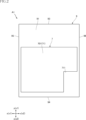
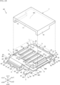
- FIG. 1 is a partial exploded perspective view showing a semiconductor device according to a first embodiment of the present disclosure.
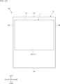
- FIG. 2 is a plan view showing the semiconductor device according to the first embodiment of the present disclosure.
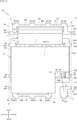
- FIG. 3 is a plan view showing the semiconductor device according to the first embodiment of the present disclosure.
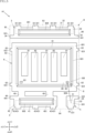
- FIG. 4 is a partial plan view showing the semiconductor device according to the first embodiment of the present disclosure.
- FIG. 5 is a partial plan view showing the semiconductor device according to the first embodiment of the present disclosure.
- FIG. 6 is a bottom view showing the semiconductor device according to the first embodiment of the present disclosure.
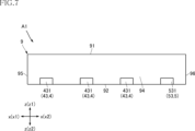
- FIG. 7 is a front view showing the semiconductor device according to the first embodiment of the present disclosure.
- FIG. 8 is a rear view showing the semiconductor device according to the first embodiment of the present disclosure.
- FIG. 1 is a partial exploded perspective view showing a semiconductor device according to a first embodiment of the present disclosure.
- FIG. 2 is a plan view showing the semiconductor device according to the first embodiment of the present disclosure.
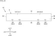
- FIG. 9 is a left side view showing the semiconductor device according to the first embodiment of the present disclosure.
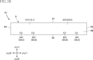
- FIG. 10 is a right side view showing the semiconductor device according to the first embodiment of the present disclosure.
- FIG. 11 is a cross-sectional view taken along line XI-XI in FIG.
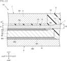
- FIG. 12 is a partially enlarged cross-sectional view showing the semiconductor device according to the first embodiment of the present disclosure.
- FIG. 13 is a cross-sectional view taken along line XIII-XIII in FIG.
- FIG. 14 is a partially enlarged cross-sectional view showing the semiconductor device according to the first embodiment of the present disclosure.
- FIG. 15 is a cross-sectional view taken along line XV-XV in FIG.
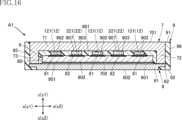
- FIG. 16 is a cross-sectional view taken along line XVI-XVI in FIG.
- FIG. 17 is a partially enlarged cross-sectional view showing the semiconductor device according to the first embodiment of the present disclosure.
- FIG. 18 is a partial exploded perspective view showing a semiconductor device according to the second embodiment of the present disclosure.
- FIG. 19 is a plan view showing a semiconductor device according to a second embodiment of the present disclosure.
- FIG. 20 is a plan view showing a semiconductor device according to a second embodiment of the present disclosure.
- FIG. 21 is a partial plan view showing a semiconductor device according to a second embodiment of the present disclosure.
- FIG. 22 is a partial plan view showing a semiconductor device according to a second embodiment of the present disclosure.
- FIG. 23 is a bottom view showing the semiconductor device according to the second embodiment of the present disclosure.
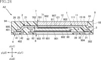
- FIG. 24 is a cross-sectional view taken along line XXIV-XXIV in FIG.
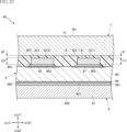
- FIG. 25 is a partially enlarged cross-sectional view showing a semiconductor device according to a second embodiment of the present disclosure.
- 26 is a cross-sectional view taken along line XXVI-XXVI in FIG. 21.
- FIG. 27 is a partially enlarged cross-sectional view showing a semiconductor device according to a second embodiment of the present disclosure.
- 28 is a cross-sectional view taken along line XXVIII-XXVIII in FIG. 21.
- FIG. FIG. 29 is a cross-sectional view taken along line XXIX-XXIX in FIG.
- FIG. 30 is a partially enlarged cross-sectional view showing a semiconductor device according to a second embodiment of the present disclosure.
- FIG. 31 is a circuit diagram showing an example of a DC/DC converter in which the semiconductor device according to the second embodiment of the present disclosure is used.
- FIG. 32 is a partially enlarged cross-sectional view showing a semiconductor device according to a third embodiment of the present disclosure.
- FIG. 33 is a cross-sectional view showing a semiconductor device according to a fourth embodiment of the present disclosure.
- FIG. 34 is a partial perspective view showing a semiconductor device according to a fifth embodiment of the present disclosure.
- FIG. 35 is a partially enlarged cross-sectional view showing a semiconductor device according to a fifth embodiment of the present disclosure.
- FIG. 31 is a circuit diagram showing an example of a DC/DC converter in which the semiconductor device according to the second embodiment of the present disclosure is used.
- FIG. 32 is a partially enlarged cross-sectional view showing a semiconductor device according to a third embodiment of the present
- FIG. 36 is a cross-sectional view showing a semiconductor device according to the sixth embodiment of the present disclosure.
- FIG. 37 is a partially enlarged cross-sectional view showing a semiconductor device according to a sixth embodiment of the present disclosure.
- FIG. 38 is a partially enlarged cross-sectional view showing a semiconductor device according to the seventh embodiment of the present disclosure.
- FIG. 39 is a cross-sectional view showing a semiconductor device according to the eighth embodiment of the present disclosure.
- an object A is formed on an object B" and “an object A is formed on an object B” include “an object A is formed directly on an object B” and “an object A is formed on an object B with another object interposed between the object A and the object B” unless otherwise specified.
- an object A is disposed on an object B” and “an object A is disposed on an object B” include “an object A is disposed directly on an object B” and “an object A is disposed on an object B with another object interposed between the object A and the object B" unless otherwise specified.
- an object A is located on an object B includes “an object A is located on an object B in contact with an object B” and “an object A is located on an object B with another object interposed between the object A and the object B” unless otherwise specified.
- an object A overlaps an object B when viewed in a certain direction includes “an object A overlaps the entire object B” and “an object A overlaps a part of an object B.”
- a surface A faces in direction B is not limited to the case where the angle of surface A with respect to direction B is 90°, but also includes the case where surface A is tilted with respect to direction B.
- First embodiment: 1 to 17 show a semiconductor device according to a first embodiment of the present disclosure.
- the semiconductor device A1 of this embodiment includes a plurality of leads 1 to 6, a heat dissipation member 7, a semiconductor element 8, a wire 909, and a sealing resin 9.
- the semiconductor device A1 is intended to perform current switching by being mounted on a substrate, for example, but the specific use of the semiconductor device A1 is not limited in any way.
- the thickness direction of the semiconductor device A1 (e.g., the up-down direction in FIG. 1) will be referred to as the thickness direction z.
- a direction orthogonal to the thickness direction z will be referred to as the first direction x.
- a direction orthogonal to the thickness direction z and the first direction x will be referred to as the second direction y.
- the multiple leads 1 to 6 are intended to appropriately fulfill the functions of supporting the semiconductor element 8, forming a conductive path that is electrically connected to the semiconductor element 8, and the like.
- the multiple leads 1 to 6 include metals such as Cu (copper), Ni (nickel), Fe (iron), etc., or alloys thereof.
- the multiple leads 1 to 6 are formed, for example, by subjecting a metal plate material to a process selected from punching, bending, etching, etc.
- a plating layer containing Ag (silver), Ni (nickel), Au (gold), etc. may be provided at appropriate locations on each of the multiple leads 1 to 6 as necessary.
- the multiple leads 1 to 6 are described as a drain lead 1, a source lead 2, a drain terminal lead 3, a source terminal lead 4, a gate terminal lead 5, and an island lead 6. That is, the multiple leads 1 to 6 include a drain lead 1, a source lead 2, a drain terminal lead 3, a source terminal lead 4, a gate terminal lead 5, and an island lead 6. As described below, in this embodiment, the source terminal lead 4 and the island lead 6 are connected to each other. Depending on the conduction form of each lead 1 to 6, they may be configured as separate pieces, or any of the leads may be connected to each other.
- the island lead 6 has a main surface 601, a back surface 602, a thick portion 61, a thin portion 62, and a plurality of extending portions 63.
- the main surface 601 is a surface facing the z1 side of the thickness direction z, and in the illustrated example, is a flat surface perpendicular to the thickness direction z.
- the island lead 6 may have, for example, a recess or a groove recessed from the main surface 601 as appropriate.
- the back surface 602 is a surface facing the z2 side of the thickness direction z, and is facing the opposite side to the main surface 601. In the illustrated example, the back surface 602 is a flat surface perpendicular to the thickness direction z.
- a plating layer including Ni (nickel), Ti (titanium), or the like may be provided on the back surface 602 as appropriate.
- the thick portion 61 is a portion where the main surface 601 and the back surface 602 overlap when viewed in the thickness direction z, and in the illustrated example, is a rectangular portion when viewed in the thickness direction z.
- the shape of the thick portion 61 is not limited in any way.
- the thickness of the thick portion 61 in the thickness direction z is the distance between the main surface 601 and the back surface 602.
- the thin portion 62 is a portion that overlaps with the main surface 601 when viewed in the thickness direction z, but does not overlap with the back surface 602, and in the illustrated example, is connected so as to extend from the thick portion 61 to both sides in the first direction x and both sides in the second direction y when viewed in the thickness direction z.
- the thickness of the thin portion 62 in the thickness direction z is smaller than the distance between the main surface 601 and the back surface 602.
- the thickness of the thick portion 61 and the thickness of the thin portion 62 are not limited in any way.
- the thickness of the thick portion 61 is about 0.2 mm to 0.5 mm
- the thickness of the thin portion 62 is 0.1 mm to 0.4 mm.
- the portion of the thin portion 62 that extends from the thick portion 61 to the y1 side in the second direction y is larger than the portion that extends to the y2 side.
- the multiple extensions 63 are portions extending from the ends of the thin-walled portion 62. In the illustrated example, the multiple extensions 63 extend from the thin-walled portion 62 on both sides in the first direction x.
- the number of extensions 63 is not limited in any way, and may be multiple or may be one. In the illustrated example, two extensions 63 are provided on the x1 side of the first direction x, and two extensions 63 are provided on the x2 side.
- the extensions 63 have end faces 631.
- the end faces 631 are faces facing the opposite side to the thin-walled portion 62 in the first direction x, in other words, faces outward in the first direction x.
- the illustrated end faces 631 are faces perpendicular to the first direction x.
- the positions in the first direction x of the two end faces 631 located on the x1 side of the first direction x are the same.
- the positions in the first direction x of the two end faces 631 located on the x2 side of the first direction x are the same.
- Drain Lead 1 1, 3, 4, 11 to 14, and 16 the drain lead 1 is disposed on the z1 side in the thickness direction z relative to the drain terminal lead 3, the source terminal lead 4, the gate terminal lead 5, and the island lead 6.
- the drain lead 1 of this embodiment has a main portion 11, a plurality of comb portions 12, a connecting portion 15, and a joint portion 16.
- the drain lead 1 of this embodiment is an example of the second lead of the present disclosure.
- the main portion 11 is a plate-like portion along the xy plane, and in the illustrated example, is rectangular (or approximately rectangular) with the first direction x as the longitudinal direction.
- the main portion 11 has a surface 111.
- the surface 111 is a surface facing the z1 side in the thickness direction z. In the illustrated example, the surface 111 is a flat surface.
- the multiple comb portions 12 extend from the main portion 11 toward the y2 side in the second direction y. There is no limitation on the number of comb portions 12, and in the illustrated example, three comb portions 12 are provided. The multiple comb portions 12 are arranged side by side in the first direction x. The comb portions 12 in this embodiment are an example of the second comb portions of the present disclosure.
- the comb portion 12 is a portion located on the y2 side of the main portion 11 in the second direction y.
- the shape of the comb portion 12 is not limited in any way, and in the illustrated example, it has a shape whose longitudinal direction is the second direction y when viewed along the thickness direction z.
- the comb portion 12 is perpendicular to the thickness direction z.
- the three comb portions 12 include a comb portion 12 whose length in the second direction y is different from that of the other comb portions 12.
- the comb portion 12 located in the center in the first direction x has a longer length in the second direction y than the other comb portions 12.
- the comb portions 12 located on both sides in the first direction x are positioned close to a gate electrode 83 described below.
- the comb portion 12 located on the x2 side of the first direction x is positioned close to a gate electrode 83 and a wire 909 described below.
- the multiple comb portions 12 may be of equal length.
- the comb portion 12 has a surface 121.
- the surface 121 in this embodiment is an example of the second surface of the present disclosure.
- the surface 121 is a surface facing the z1 side in the thickness direction z.
- the surface 121 is a flat surface.
- the surface 121 is located on the z2 side in the thickness direction z from the surface 111.
- the thickness t11 of the comb portion 12 is thinner than the thickness t10 of the main portion 11.
- Such a drain lead 1 can be formed, for example, by selectively etching the comb portion 12.
- the size of the thickness t10 and the thickness t11 is not limited in any way.
- the thickness t10 is, for example, 150 ⁇ m or more and 500 ⁇ m or less, for example, about 250 ⁇ m.
- the thickness t11 is, for example, 40% or more and 80% or less of the thickness t10, for example, about 50%.
- the comb portion 12 has a tip surface 122.
- the tip surface 122 is a surface of the comb portion 12 that is located on the y2 side in the second direction y.
- the tip surface 122 is inclined so that it is located on the z1 side in the thickness direction z as it approaches the y2 side in the second direction y.
- the connecting portion 15 is connected to the end of the main portion 11 on the y1 side in the second direction y, opposite the comb portion 12.
- the connecting portion 15 extends from the main portion 11 to the z2 side in the thickness direction z.
- the connecting portion 15 is inclined with respect to the thickness direction z.
- the center of the connecting portion 15 in the first direction x is the same as the center of the main portion 11 in the first direction x.
- the joint 16 is connected to the end of the connecting portion 15 on the y1 side in the second direction y.
- the joint 16 is aligned along the first direction x and the second direction y.
- the joint 16 is rectangular with the first direction x as its longitudinal direction.
- the center of the joint 16 in the first direction x is the same as the center of the connecting portion 15 in the first direction x.
- the joint 16 is conductively joined to the drain terminal lead 3 via a fourth conductive joint 904.
- the fourth conductive joint 904 is, for example, solder, Ag paste material, Ag sintered material, Cu sintered material, etc.
- Source Read 2 1, 4, 11, 13, 14, and 16
- the source lead 2 is disposed on the z1 side in the thickness direction z relative to the drain terminal lead 3, the source terminal lead 4, the gate terminal lead 5, and the island lead 6.
- the source lead 2 is disposed on the y2 side in the second direction y relative to the drain lead 1.
- the source lead 2 in this embodiment has a main portion 21, a plurality of comb portions 22, a connecting portion 25, and a joint portion 26.
- the source lead 2 in this embodiment is an example of a first lead of the present disclosure.
- the main portion 21 is a plate-like portion along the xy plane, and in the illustrated example, is rectangular (or approximately rectangular) with the first direction x as the longitudinal direction.
- the main portion 11 and the main portion 21 are disposed on opposite sides of each other in the second direction y with respect to the semiconductor element 8.
- the main portion 21 has a surface 211.
- the surface 211 is a surface facing the z1 side in the thickness direction z. In the illustrated example, the surface 211 is a flat surface.
- the multiple comb portions 22 extend from the main portion 21 toward the y1 side in the second direction y. There is no limitation on the number of comb portions 22, and in the illustrated example, two comb portions 22 are provided. The multiple comb portions 22 are arranged side by side in the first direction x. The comb portions 22 in this embodiment are an example of the first comb portions of the present disclosure.
- the comb portion 22 is a portion located on the y1 side of the main portion 21 in the second direction y.
- the shape of the comb portion 22 is not limited in any way, and in the illustrated example, it has a shape whose longitudinal direction is the second direction y when viewed along the thickness direction z.
- the comb portion 22 is perpendicular to the thickness direction z.
- the lengths of the two comb portions 22 in the second direction y are equal. However, the lengths of the multiple comb portions 22 in the second direction y may be different from each other.
- the comb portion 22 has a surface 221.
- the surface 221 in this embodiment is an example of a first surface of the present disclosure.
- the surface 221 is a surface facing the z1 side in the thickness direction z.
- the surface 221 is a flat surface.
- the surface 221 is located at the same position in the thickness direction z as the surface 211.
- the surfaces 221 and 211 are flush with each other.
- the thickness t20 of the main portion 21 and the thickness t21 of the comb portion 22 are the same.
- the thickness t11 is thinner than the thickness t21.
- the thicknesses t20 and t21 are, for example, 150 ⁇ m or more and 500 ⁇ m or less, for example, about 250 ⁇ m.
- the comb portion 22 has a tip surface 222.
- the tip surface 222 is a surface of the comb portion 22 that is located on the y1 side of the second direction y.
- the tip surface 222 is inclined so that it is located on the z1 side in the thickness direction z as it approaches the y1 side in the second direction y.
- the connecting portion 25 is connected to the end of the main portion 21 on the y2 side in the second direction y, opposite the comb portion 22.
- the connecting portion 25 extends from the main portion 21 to the z2 side in the thickness direction z.
- the connecting portion 25 is inclined with respect to the thickness direction z.
- the shape of the connecting portion 25 is not limited in any way, and in the illustrated example, it is rectangular with the first direction x as its longitudinal direction. In the illustrated example, the center of the connecting portion 25 in the first direction x is located on the x1 side in the first direction x with respect to the center of the main portion 21 in the first direction x.
- the joint 26 is connected to the end of the connecting portion 25 on the y2 side in the second direction y.
- the joint 26 is aligned along the first direction x and the second direction y.
- the joint 26 is rectangular with the first direction x as its longitudinal direction.
- the center of the joint 26 in the first direction x is the same as the center of the connecting portion 25 in the first direction x.
- the joint 26 is conductively joined to the source terminal lead 4 via a fifth conductive joint 905.
- the fifth conductive joint 905 is, for example, solder, Ag paste material, Ag sintered material, Cu sintered material, etc.
- Drain terminal lead 3 1, 3 to 6, 11, 13 and 15, the drain terminal lead 3 is disposed at a distance from the island lead 6 on the y1 side in the second direction y.
- the center of the drain terminal lead 3 in the first direction x is at approximately the same position in the first direction x as the center of the island lead 6 in the first direction x.
- the drain terminal lead 3 has a main surface 301, a back surface 302, a thick portion 31, a thin portion 32, a plurality of extending portions 33, and a plurality of end faces 341.
- the main surface 301 is a surface facing the z1 side in the thickness direction z, and in the illustrated example, is a flat surface perpendicular to the thickness direction z.
- the drain terminal lead 3 may have, for example, a recess or a groove recessed from the main surface 301 as appropriate.
- the joint 16 is joined to the main surface 301 via the fourth conductive joint 904.
- the back surface 302 is a surface facing the z2 side in the thickness direction z, and faces the opposite side to the main surface 301. In the illustrated example, the back surface 302 is a flat surface perpendicular to the thickness direction z.
- a plating layer containing Ni (nickel), Ti (titanium), or the like may be provided on the back surface 302 as appropriate.
- the main surface 301 is located at approximately the same position as the main surface 601 in the thickness direction z
- the back surface 302 is located at approximately the same position as the back surface 602.
- the thick portion 31 is a portion where the main surface 301 and the back surface 302 overlap when viewed in the thickness direction z.
- the thick portion 31 is a rectangular portion with the first direction x as the longitudinal direction when viewed in the thickness direction z.
- the shape of the thick portion 31 is not limited in any way.
- the thickness of the thick portion 31 in the thickness direction z is the distance between the main surface 301 and the back surface 302.
- the thin portion 32 is a portion that overlaps the main surface 301 when viewed in the thickness direction z and does not overlap the back surface 302.
- the thin portion 32 is connected to the thick portion 31 so as to extend from both sides of the first direction x and to the y2 side of the second direction y when viewed in the thickness direction z.
- the thin portion 32 has a portion that is connected to the thick portion 31 so as to extend from the thick portion 31 to the y1 side of the second direction y when viewed in the thickness direction z, and this portion is sandwiched between the extension portions 33 in the first direction x.
- the thickness of the thin portion 32 in the thickness direction z is smaller than the distance between the main surface 301 and the back surface 302.
- the thicknesses of the thick portion 31 and the thin portion 32 are not limited in any way. In this embodiment, the thickness of the thick portion 31 is approximately the same as the thickness of the thick portion 61, and the thickness of the thin portion 32 is approximately the same as the thickness of the thin portion 62.
- the multiple extension portions 33 are portions that extend from the end of the thick portion 31. In the illustrated example, the multiple extension portions 33 extend from the thick portion 31 toward the y1 side in the second direction y. There is no limitation on the number of extension portions 33, and there may be multiple extension portions 33 or there may be only one extension portion. In the illustrated example, four extension portions 33 are provided.
- the extension portion 33 has an end face 331.
- the end face 331 is a surface that faces the opposite side to the thick portion 31 in the second direction y, in other words, a surface that faces the y1 side, which is the outside, in the second direction y.
- the illustrated end face 331 is a surface that is perpendicular to the second direction y.
- the multiple end faces 331 are located at the same position in the second direction y.
- the multiple extension portions 34 are portions extending from the end of the thin-walled portion 32. In the illustrated example, the multiple extension portions 34 extend from the thin-walled portion 32 in the first direction. There is no limitation on the number of extension portions 34, and there may be multiple extension portions 34 or just one extension portion. In the illustrated example, two extension portions 34 are provided.
- the extension portion 34 has an end face 341.
- the end face 341 is a surface facing the first direction x.
- the illustrated end face 341 is a surface perpendicular to the first direction x.
- the two end faces 341 face opposite each other in the first direction x.
- Source terminal lead 4 As shown in FIG. 1, FIG. 3 to FIG. 6, FIG. 11, and FIG. 13, the source terminal lead 4 is disposed on the y2 side of the island lead 6 in the second direction y. The center of the source terminal lead 4 in the first direction x is located on the x1 side of the center of the island lead 6 in the first direction x. In the semiconductor device A1, the source terminal lead 4 and the island lead 6 are connected by a relay portion 49. In the illustrated example, two relay portions 49 are provided apart from each other in the first direction x. The number of relay portions 49 is not limited in any way. Unlike this configuration, the source terminal lead 4 may be separated from the island lead 6.
- the source terminal lead 4 has a main surface 401, a back surface 402, a thick portion 41, a thin portion 42, and a plurality of extending portions 43 and 44.
- the main surface 401 is a surface facing the z1 side in the thickness direction z, and in the illustrated example, is a flat surface perpendicular to the thickness direction z.
- the source terminal lead 4 may have, for example, a recess or a groove recessed from the main surface 401 as appropriate.
- the joint 26 is joined to the main surface 401 via a fifth conductive joint 905.
- the back surface 402 is a surface facing the z2 side in the thickness direction z, and faces the opposite side to the main surface 401. In the illustrated example, the back surface 402 is a flat surface perpendicular to the thickness direction z.
- a plating layer containing Ni (nickel), Ti (titanium), or the like may be provided on the back surface 402 as appropriate.
- the main surface 401 is located at approximately the same position as the main surface 601 in the thickness direction z
- the back surface 402 is located at approximately the same position as the back surface 602.
- the thick portion 41 is a portion where the main surface 401 and the back surface 402 overlap when viewed in the thickness direction z.
- the thick portion 41 is a rectangular portion with the first direction x as the longitudinal direction when viewed in the thickness direction z.
- the shape of the thick portion 41 is not limited in any way.
- the thickness of the thick portion 41 in the thickness direction z is the distance between the main surface 401 and the back surface 402.
- the dimension of the thick portion 41 in the first direction x is smaller than the dimension of the thick portion 31 in the first direction x.
- the thin portion 42 is a portion that overlaps with the main surface 401 when viewed in the thickness direction z, but does not overlap with the back surface 402.
- the thin portion 42 is connected so as to extend from the thick portion 41 to both sides in the first direction x and to the y1 side in the second direction y when viewed in the thickness direction z.
- the thin portion 42 has a portion that is connected to the thick portion 41 so as to extend to the y2 side in the second direction y when viewed in the thickness direction z, and this portion is sandwiched between the extending portions 43 in the first direction x.
- the thickness of the thin portion 42 in the thickness direction z is smaller than the distance between the main surface 401 and the back surface 402.
- the thicknesses of the thick portion 41 and the thin portion 42 are not limited in any way. In this embodiment, the thickness of the thick portion 41 is approximately the same as the thickness of the thick portion 61, and the thickness of the thin portion 42 is approximately the same as the thickness of the thin portion 62.
- the multiple extensions 43 are portions extending from the end of the thick portion 41.
- the multiple extensions 43 extend from the thick portion 41 toward the y2 side in the second direction y.
- the number of extensions 43 is not limited in any way, and may be multiple or may be one.
- three extensions 43 are provided.
- the positions of these three extensions 43 in the first direction x are approximately the same as the positions of the three extensions 33 located on the x1 side in the first direction x among the multiple extensions 33 in the first direction x.
- the extension 43 has an end face 431.
- the end face 431 is a face facing the opposite side to the thick portion 41 in the second direction y, in other words, a face facing the y2 side, which is the outside, in the second direction y.
- the illustrated end face 431 is a face perpendicular to the second direction y.
- the positions of the multiple end faces 431 in the second direction y are the same as each other.
- the extension portion 44 is a portion that extends from the end of the thin portion 42. In the illustrated example, the extension portion 44 extends from the thin portion 42 toward the x1 side of the first direction x. There is no limitation on the number of extension portions 44, and there may be multiple extension portions or only one extension portion. In the illustrated example, one extension portion 44 is provided.
- the extension portion 44 has an end face 441.
- the end face 441 is a surface that faces the x1 side of the first direction x.
- the illustrated end face 441 is a surface that is perpendicular to the first direction x.
- the island lead 6 is electrically connected to the source electrode 82 of the semiconductor element 8 via the source lead 2 and the source terminal lead 4.
- Gate terminal lead 5 1, 3 to 6, and 15, the gate terminal lead 5 is disposed on the y2 side in the second direction y with respect to the island lead 6.
- the center of the gate terminal lead 5 in the first direction x is located on the x2 side in the first direction x with respect to the center of the island lead 6 in the first direction x.
- the gate terminal lead 5 is disposed on the x2 side in the first direction x with respect to the source terminal lead 4.
- the gate terminal lead 5 has a main surface 501, a back surface 502, a thick portion 51, a thin portion 52, an extending portion 53, and an extending portion 54.
- the main surface 501 faces the z1 side in the thickness direction z, and in the illustrated example, is a flat surface perpendicular to the thickness direction z.
- the gate terminal lead 5 may have, for example, a recess or a groove recessed from the main surface 501 as appropriate.
- a wire 909 is bonded to the main surface 501.
- the back surface 502 faces the z2 side in the thickness direction z, and faces the opposite side to the main surface 501. In the illustrated example, the back surface 502 is a flat surface perpendicular to the thickness direction z.
- a plating layer containing Ni (nickel), Ti (titanium), or the like may be provided on the back surface 502 as appropriate.
- the main surface 501 is located at approximately the same position as the main surface 601 in the thickness direction z
- the back surface 502 is located at approximately the same position as the back surface 602.
- the thick portion 51 is a portion where the main surface 501 and the back surface 502 overlap when viewed in the thickness direction z.
- the thick portion 51 is a rectangular portion when viewed in the thickness direction z.
- the shape of the thick portion 51 is not limited in any way.
- the thickness of the thick portion 51 in the thickness direction z is the distance between the main surface 501 and the back surface 502.
- the dimension of the thick portion 51 in the first direction x is smaller than the dimensions of the thick portion 31 and the thick portion 41 in the first direction x.
- the thin portion 32 is a portion that overlaps with the main surface 301 when viewed in the thickness direction z, but does not overlap with the back surface 302.
- the thin portion 32 is connected so as to extend from the thick portion 51 to both sides in the first direction x and to the y1 side in the second direction y when viewed in the thickness direction z.
- the thickness of the thin portion 52 in the thickness direction z is smaller than the distance between the main surface 501 and the back surface 502.
- the thickness of the thick portion 51 and the thin portion 52 are no limitations.
- the thickness of the thick portion 51 is approximately the same as the thickness of the thick portion 61
- the thickness of the thin portion 52 is approximately the same as the thickness of the thin portion 62.
- the extension portion 53 is a portion extending from the end of the thick portion 51. In the illustrated example, the extension portion 53 extends from the thick portion 51 toward the y2 side in the second direction y. There is no limitation on the number of extension portions 53, and there may be multiple extension portions 53 or there may be only one extension portion. In the illustrated example, one extension portion 53 is provided. The position of the extension portion 53 in the first direction x is approximately the same as the position of the extension portion 33 located closest to the x2 side in the first direction x among the multiple extension portions 33. The extension portion 53 has an end face 531.
- the end face 531 is a face facing the opposite side to the thick portion 51 in the second direction y, in other words, a face facing the y2 side, which is the outside, in the second direction y.
- the illustrated end face 531 is a face perpendicular to the second direction y.
- the position of the end face 531 in the second direction y is the same as the multiple end faces 431.
- the extension portion 54 is a portion extending from the end of the thin portion 52. In the illustrated example, the extension portion 54 extends from the thin portion 52 toward the x2 side in the first direction x. There is no limitation on the number of extension portions 54, and there may be multiple extension portions 54 or there may be only one extension portion. In the illustrated example, one extension portion 54 is provided.
- the position of the extension portion 54 in the second direction y is approximately the same as the position of the extension portion 44 in the second direction y.
- the extension portion 54 has an end face 541.
- the end face 541 is a face facing the opposite side to the thick portion 51 in the first direction x, in other words, a face facing the x2 side, which is the outside, in the first direction x.
- the illustrated end face 541 is a face perpendicular to the first direction x.
- the position of the end face 541 in the second direction y is the same as the end face 341 and the multiple end faces 631.
- the heat dissipation member 7 is a member that functions to dissipate heat generated from the semiconductor element 8 to the outside of the semiconductor device A1.
- the material of the heat dissipation member 7 is not limited in any way, and includes, for example, metals such as Cu (copper), Ni (nickel), Fe (iron), etc., or alloys thereof.
- the heat dissipation member 7 is formed, for example, by subjecting a metal plate material to a process selected from punching, bending, etching, etc.
- a plating layer containing Ag (silver), Ni (nickel), Au (gold), etc. may be provided at appropriate locations of the heat dissipation member 7 as necessary.
- the shape of the heat dissipation member 7 is not limited in any way. As shown in Figures 1 to 3 and 11 to 17, in this embodiment, the heat dissipation member 7 has a main portion 71, a support portion 72, and a support portion 73.
- the main portion 71 is disposed on the z1 side of the semiconductor element 8 in the z direction.
- the shape of the main portion 71 is not limited in any way, and in the illustrated example, it is a flat portion along the first direction x and the second direction y.
- the main portion 71 overlaps with the semiconductor element 8, and in the illustrated example, it overlaps with most of the semiconductor element 8.
- the main portion 71 overlaps with the multiple comb portions 12 and the multiple comb portions 22.
- the main portion 71 has a main heat dissipation surface 701 and a back heat dissipation surface 702.
- the main heat dissipation surface 701 is a surface facing the z1 side in the z direction. In the illustrated example, the main heat dissipation surface 701 is a flat surface.
- the back heat dissipation surface 702 is a surface facing the z2 side in the z direction. In the illustrated example, the back heat dissipation surface 702 is a flat surface.
- the main portion 71 has a recess 711.
- the recess 711 is a portion of the main portion 71 that is recessed toward the x1 side in the first direction x and toward the y1 side in the second direction y. Due to the formation of the recess 711, the gate electrode 83 and the wire 909 located on the x2 side in the first direction x do not overlap with the main portion 71 when viewed in the z direction.
- the support portion 72 is connected to the end of the main portion 71 on the x2 side in the first direction x, and extends to the x2 side in the z direction.
- the support portion 72 has a shape whose longitudinal direction is the second direction y. In the illustrated example, a part of the support portion 72 protrudes from the main portion 71 on the y2 side in the second direction y.
- the support portion 73 is connected to the end portion of the main portion 71 on the x1 side in the first direction x, and extends to the x2 side in the z direction.
- the support portion 72 has a shape whose longitudinal direction is in the second direction y.
- the size in the second direction y of the support portion 73 is the same as the size in the second direction y of the support portion 72, and is smaller than the size in the second direction y of the end portion of the main portion 71 on the x1 side in the first direction x.
- Sixth conductive joint portion 906 is, for example, solder, Ag paste material, Ag sintered material, Cu sintered material, etc.
- the heat dissipating back surface 702 is joined to the front surface 221 of the multiple comb portions 22 via the seventh conductive joint 907.
- the seventh conductive joint 907 is, for example, solder, Ag paste material, Ag sintered material, Cu sintered material, etc.
- the gap g2 between the front surface 221 and the heat dissipating main surface 701 is filled by the seventh conductive joint 907.
- the size of the gap g2 is not limited in any way and is, for example, 10 ⁇ m or more and 30 ⁇ m or less.
- the heat dissipating back surface 702 is joined to the main portion 21 via the seventh conductive joint 907. Depending on the shape of the main portion 71, etc., the heat dissipating back surface 702 may not be joined to the main portion 21.
- a portion of the sealing resin 9 is filled between the heat dissipating back surface 702 and the surfaces 121 of the multiple comb portions 12. This insulates the heat dissipating member 7 from the multiple comb portions 12.
- the main portion 71 does not cover the main portion 11 when viewed from the z direction. Therefore, even if the thickness t10 of the main portion 11 is the same as the thickness t20 and the thickness t21, the main portion 11 is not joined to or in contact with the main portion 71 of the heat dissipating member 7.
- the semiconductor element 8 is an element that exerts the electrical function of the semiconductor device A1.
- the specific configuration of the semiconductor element 8 is not limited in any way, and in this embodiment, the semiconductor element 8 is a transistor using a nitride semiconductor, more specifically, a GaN-HEMT (High Electron Mobility Transistor) element using gallium nitride (GaN).
- the semiconductor element 8 is not limited to one using a nitride semiconductor, and other semiconductors such as silicon (Si) and silicon carbide (SiC) may be used.
- the semiconductor element 8 is not limited to a HEMT, and may be other transistors such as a MOSFET (Metal-Oxide-Semiconductor Field Effect Transistor) and an IGBT (Insulated Gate Bipolar Transistor).
- the semiconductor element 8 is mounted on the thick portion 61 of the island lead 6. As shown in FIG. 1, FIG. 3 to FIG. 5, and FIG. 11 to FIG. 16, the semiconductor element 8 has an element body 80, a plurality of drain electrodes 81, a plurality of source electrodes 82, and a gate electrode 83.
- the element body 80 is, for example, a portion in which a substrate layer, a buffer layer, and a nitride semiconductor layer are stacked.
- the element body 80 has an element main surface 801 and an element back surface 802.
- the element main surface 801 is a surface facing the z1 side in the thickness direction z.
- the element back surface 802 is a surface facing the z2 side in the thickness direction z, and faces the opposite side to the element main surface 801.
- a metal layer 89 is provided on the element back surface 802. This metal layer 89 and the main surface 601 of the island lead 6 are joined by a first conductive joint 901.
- the first conductive joint 901 is, for example, solder, Ag paste material, Ag sintered material, Cu sintered material, etc.
- the metal layer 89 is provided for joining by the first conductive joint 901, but the metal layer 89 may not be provided. Alternatively, the metal layer 89 may be configured to have the same potential as, for example, the source electrode 82, etc.
- the semiconductor element 8 is positioned so that it overlaps a portion of the thick portion 61 and a portion of the thin portion 62 of the island lead 6 when viewed in the thickness direction z.
- the drain electrodes 81, the source electrodes 82, and the gate electrode 83 are arranged on the main surface 801 of the element.
- the number of the drain electrodes 81 and the source electrodes 82 is not limited in any way. In the illustrated example, three drain electrodes 81 and two source electrodes 82 are provided.
- the number of the drain electrodes 81 is the same as the number of the comb portions 12, and the number of the source electrodes 82 is the same as the number of the comb portions 22.
- the drain electrode 81 of this embodiment is an example of the second electrode of the present disclosure.
- the source electrode 82 of this embodiment is an example of the first electrode of the present disclosure.
- the drain electrodes 81 and the source electrodes 82 are arranged alternately in the first direction x.
- the shapes of the drain electrodes 81 and the source electrodes 82 are not limited in any way, and in the illustrated example, they are shaped such that the second direction y is the longitudinal direction, and more specifically, are rectangular.
- the multiple comb portions 12 of the drain lead 1 are individually conductively joined to the multiple drain electrodes 81 via second conductive joints 902.
- the second conductive joints 902 are, for example, solder, Ag paste material, Ag sintered material, Cu sintered material, etc.
- the multiple comb portions 22 of the source lead 2 are individually conductively joined to the multiple source electrodes 82 via third conductive joints 903.
- the third conductive joints 903 are, for example, solder, Ag paste material, Ag sintered material, Cu sintered material, etc.
- the number of gate electrodes 83 is not limited, and may be one or more. In the illustrated example, two gate electrodes 83 are provided. The two gate electrodes 83 are arranged apart in the first direction x. A wire 909 is joined to the gate electrode 83 arranged on the x2 side of the first direction x, and is electrically connected to the gate terminal lead 5 via the wire 909. Instead of the wire 909, a conductive member made of a metal plate material may be used to electrically connect the gate electrode 83 and the gate terminal lead 5. In the illustrated example, the gate electrode 83 on the x1 side of the first direction x is not electrically used.
- the sealing resin 9 covers a portion of each of the leads 1 to 6, a portion of the heat dissipation member 7, the semiconductor element 8, and the wires 909, and is made of an insulating material such as an epoxy resin. As shown in Figures 2 to 16, the sealing resin 9 has a first resin surface 91, a second resin surface 92, a third resin surface 93, a fourth resin surface 94, a fifth resin surface 95, and a sixth resin surface 96, and is in the shape of a rectangular parallelepiped.
- the resin first surface 91 is a surface facing the z1 side in the thickness direction z.
- the resin first surface 91 is a plane perpendicular to the thickness direction z.
- the resin second surface 92 is a surface facing the z2 side in the thickness direction z.
- the resin second surface 92 is a plane perpendicular to the thickness direction z.
- the resin third surface 93 is a surface facing the y1 side in the second direction y.
- the resin third surface 93 is a plane perpendicular to the second direction y.
- the resin fourth surface 94 is a surface facing the y2 side in the second direction y.
- the resin fourth surface 94 is a plane perpendicular to the second direction y.
- the resin fifth surface 95 is a surface facing the x1 side in the first direction x.
- the resin fifth surface 95 is a plane perpendicular to the first direction x.
- the sixth resin surface 96 is a surface facing the x2 side in the first direction x.
- the sixth resin surface 96 is a plane perpendicular to the first direction x.
- the main heat dissipation surface 701 of the heat dissipation member 7 is exposed on the z1 side in the thickness direction z from the first resin surface 91.
- the first resin surface 91 and the main heat dissipation surface 701 are flush with each other. However, the main heat dissipation surface 701 may protrude slightly from the first resin surface 91.
- the back surface 602 of the island lead 6, the back surface 302 of the drain terminal lead 3, the back surface 402 of the source terminal lead 4, and the back surface 502 of the gate terminal lead 5 are exposed on the z2 side in the thickness direction z.
- the resin second surface 92, the back surface 602 of the island lead 6, the back surface 302 of the drain terminal lead 3, the back surface 402 of the source terminal lead 4, and the back surface 502 of the gate terminal lead 5 are flush with one another.
- all or any of the back surface 602 of the island lead 6, the back surface 302 of the drain terminal lead 3, the back surface 402 of the source terminal lead 4, and the back surface 502 of the gate terminal lead 5 may protrude slightly from the resin second surface 92.
- the multiple end faces 431 of the source terminal lead 4 and the end face 531 of the gate terminal lead 5 are exposed on the y2 side in the second direction y.
- the fourth resin surface 94, the multiple end faces 431 of the source terminal lead 4, and the end face 531 of the gate terminal lead 5 are flush with one another. However, all or any of the multiple end faces 431 of the source terminal lead 4 and the end face 531 of the gate terminal lead 5 may protrude slightly from the fourth resin surface 94.
- the end face 341 of the drain terminal lead 3, the end face 441 of the source terminal lead 4, and the multiple end faces 631 of the island lead 6 are exposed on the x1 side of the first direction x.
- the fifth resin surface 95, the end face 341 of the drain terminal lead 3, the end face 441 of the source terminal lead 4, and the multiple end faces 631 of the island lead 6 are flush with one another.
- all or any of the end face 341 of the drain terminal lead 3, the end face 441 of the source terminal lead 4, and the multiple end faces 631 of the island lead 6 may protrude slightly from the fifth resin surface 95.
- the end face 341 of the drain terminal lead 3, the end face 541 of the gate terminal lead 5, and the multiple end faces 631 of the island lead 6 are exposed on the x2 side of the first direction x.
- the sixth resin surface 96, the end face 341 of the drain terminal lead 3, the end face 541 of the gate terminal lead 5, and the multiple end faces 631 of the island lead 6 are flush with one another. However, all or any of the end face 341 of the drain terminal lead 3, the end face 541 of the gate terminal lead 5, and the multiple end faces 631 of the island lead 6 may protrude slightly from the sixth resin surface 96.
- the semiconductor device A1 is mounted on a circuit board (not shown) or the like, with the back surfaces 302, 402, and 502 exposed from the second resin surface 92 of the sealing resin 9 serving as mounting terminals. That is, the mounting surface of the semiconductor device A1 is the z2 side opposite the z1 side, which is the side to which the element main surface 801 of the semiconductor element 8 faces in the thickness direction z.
- the back surface 602 may be used as a heat dissipation surface for dissipating heat from the semiconductor element 8.
- the heat dissipation member 7 is joined to the island lead 6 and is exposed from the sealing resin 9. This allows the heat generated by the semiconductor element 8 to be dissipated more efficiently to the outside of the semiconductor device A1 via the island lead 6 and the heat dissipation member 7.
- the heat dissipation member 7 has a main portion 71, a support portion 72, and a support portion 73.
- the main portion 71 overlaps with the semiconductor element 8 when viewed in the thickness direction z.
- the support portions 72 and 73 are disposed on both sides of the semiconductor element 8 in a first direction x perpendicular to the thickness direction z.
- the main heat dissipation surface 701 is flush with the first resin surface 91. This makes it possible to prevent the first resin surface 91 from interfering when the main heat dissipation surface 701 is pressed against a heat sink (not shown) or the like outside the semiconductor device A1.
- the surfaces 221 of the comb portions 22 are joined to the heat dissipating back surface 702 of the heat dissipating member 7.
- the surfaces 121 of the comb portions 12 are located on the z2 side in the thickness direction z from the surface 221.
- a portion of the sealing resin 9 is filled between the surface 121 and the heat dissipating back surface 702. This makes it possible to more reliably insulate the heat dissipating member 7 from the drain lead 1 while joining the heat dissipating member 7 to the source lead 2.
- This makes it possible to increase the conductive path that is conductive to the source electrode 82, which is the first electrode, and the heat transfer path that dissipates heat from the semiconductor element 8 to the outside of the semiconductor device A1.
- the thickness t21 of the comb portion 22 is thicker than the thickness t11 of the comb portion 12. This makes it possible to reliably make the gap g1 between the front surface 121 and the heat-dissipating back surface 702 larger than the gap g2 between the front surface 221 and the heat-dissipating back surface 702. This is therefore preferable for bonding the front surface 221 to the heat-dissipating back surface 702 while keeping the front surface 121 in a non-bonded state with respect to the heat-dissipating back surface 702.
- FIGS. 18 to 35 and 36 to 39 show other embodiments of the present disclosure.
- elements that are the same as or similar to those in the above-described embodiment are given the same reference numerals as in the above-described embodiment.
- the configurations of each part in each of the modified examples and each embodiment can be combined with each other as appropriate to the extent that no technical contradictions arise.
- Second embodiment 18 to 30 show a semiconductor device according to a second embodiment of the present disclosure.
- a semiconductor device A2 of this embodiment differs from the semiconductor device A1 described above in the bonding and electrical continuity between the leads 1 to 6 and the heat dissipation member 7.
- Drain Lead 1 18, 20, 21, 24 to 27, and 29, the drain lead 1 is disposed on the z1 side in the thickness direction z of the drain terminal lead 3, the source terminal lead 4, the gate terminal lead 5, and the island lead 6.
- the drain lead 1 of this embodiment has a main portion 11, a plurality of comb portions 12, a connecting portion 15, and a joint portion 16.
- the drain lead 1 of this embodiment is an example of the first lead of the present disclosure.
- the comb portion 12 has a surface 121.
- the comb portion 12 in this embodiment is an example of a first comb portion of the present disclosure.
- the surface 121 in this embodiment is an example of a first surface of the present disclosure.
- the surface 121 is a surface facing the z1 side in the thickness direction z.
- the surface 121 is a flat surface.
- the surface 121 is at the same position in the thickness direction z as the surface 111.
- the surfaces 121 and 111 are flush with each other.
- the thickness t10 of the main portion 11 and the thickness t11 of the comb portion 12 are the same.
- the thicknesses t10 and t11 are, for example, 150 ⁇ m or more and 500 ⁇ m or less, for example, about 250 ⁇ m.
- Source Read 2 18, 21, 24, 26, 27, and 29, the source lead 2 is arranged on the z1 side in the thickness direction z relative to the drain terminal lead 3, the source terminal lead 4, the gate terminal lead 5, and the island lead 6.
- the source lead 2 is arranged on the y2 side in the second direction y relative to the drain lead 1.
- the source lead 2 of this embodiment has a main portion 21, a plurality of comb portions 22, a connecting portion 25, and a joint portion 26.
- the source lead 2 in this embodiment is an example of a second lead of the present disclosure.
- the comb portion 22 has a surface 221.
- the comb portion 22 in this embodiment is an example of the second comb portion of the present disclosure.
- the surface 221 in this embodiment is an example of the second surface of the present disclosure.
- the surface 221 is a surface facing the z1 side of the thickness direction z.
- the surface 221 is a flat surface.
- the surface 221 is located on the z2 side of the thickness direction z from the surface 211.
- the thickness t21 of the comb portion 22 is thinner than the thickness t20 of the main portion 21.
- the thickness t21 is thinner than the thickness t11.
- Such a source lead 2 can be formed, for example, by selectively etching the comb portion 22.
- the size of the thickness t20 and the thickness t21 is not limited in any way.
- the thickness t20 is, for example, 150 ⁇ m or more and 500 ⁇ m or less, for example, about 250 ⁇ m.
- Thickness t21 is, for example, 40% or more and 80% or less of thickness t20, for example, about 50%.
- Drain terminal lead 3 18, 20 to 23, 24, 26 and 28, the drain terminal lead 3 is disposed at a distance from the island lead 6 on the y1 side in the second direction y.
- the center of the drain terminal lead 3 in the first direction x is at approximately the same position in the first direction x as the center of the island lead 6 in the first direction x.
- the drain terminal lead 3 and the island lead 6 are connected by a relay portion 39.
- three relay portions 39 are provided spaced apart from each other in the first direction x. The number of relay portions 39 is not limited in any way.
- the island lead 6 is electrically connected to the drain electrode 81 of the semiconductor element 8 via the drain lead 1 and the drain terminal lead 3.
- Source terminal lead 4 18, 20 to 23, 24, and 26, the source terminal lead 4 is disposed on the y2 side in the second direction y with respect to the island lead 6.
- the center of the source terminal lead 4 in the first direction x is located on the x1 side in the first direction x with respect to the center of the island lead 6 in the first direction x.
- the source terminal lead 4 and the island lead 6 are spaced apart from each other.
- Heat dissipation member 7 The main portion 71 is disposed on the z1 side in the z direction with respect to the semiconductor element 8.
- the shape of the main portion 71 is not limited in any way, and in the illustrated example, it is a flat plate-like portion along the first direction x and the second direction y.
- the main portion 71 overlaps with the semiconductor element 8, and in the illustrated example, it overlaps with most of the semiconductor element 8.
- the main portion 71 does not overlap with the gate electrode 83 and the wire 909.
- the main portion 71 overlaps with the multiple comb portions 12 and the multiple comb portions 22.
- the heat dissipating back surface 702 is joined to the front surface 121 of the multiple comb portions 12 via the seventh conductive joint 907.
- the seventh conductive joint 907 is, for example, solder, Ag paste material, Ag sintered material, Cu sintered material, etc.
- the gap g1 between the front surface 121 and the heat dissipating main surface 701 is filled by the seventh conductive joint 907.
- the size of the gap g1 is not limited in any way and is, for example, 10 ⁇ m or more and 30 ⁇ m or less.
- the heat dissipating back surface 702 is joined to the main portion 11 via the seventh conductive joint 907. Depending on the shape of the main portion 71, etc., the heat dissipating back surface 702 may not be joined to the main portion 11.
- a portion of the sealing resin 9 is filled between the heat dissipating back surface 702 and the surfaces 221 of the multiple comb portions 22. This insulates the heat dissipating member 7 from the multiple comb portions 22.
- the main portion 71 does not cover the main portion 21 when viewed from the z direction. Therefore, even if the thickness t20 of the main portion 21 is the same as the thickness t10 and the thickness t11, the main portion 21 is not joined to or in contact with the main portion 71 of the heat dissipating member 7.
- the element body 80 of the semiconductor element 8 may further include a high-resistance layer 88.
- the high-resistance layer 88 is interposed, for example, between the substrate layer and the nitride semiconductor layer.
- at least the metal layer 89 is substantially insulated from the drain electrode 81 and the source electrode 82.
- the semiconductor device A2 is mounted on a circuit board (not shown) or the like, with the back surfaces 302, 402, and 502 exposed from the second resin surface 92 of the sealing resin 9 serving as mounting terminals. That is, the mounting surface of the semiconductor device A2 is the z2 side opposite the z1 side, which is the side to which the element main surface 801 of the semiconductor element 8 faces in the thickness direction z.
- the back surface 602 may be used as a heat dissipation surface for dissipating heat from the semiconductor element 8.
- FIG. 31 is a circuit diagram showing an example of a DC/DC converter in which the semiconductor device A2 is used.
- the DC/DC converter B1 in the figure includes the semiconductor devices A1 and A2, a power supply b11, a controller b12, an inductor b13, a capacitor b14, a load b15, and a semiconductor device b20.
- the power supply b11 is a DC power supply.
- the controller b12 includes, for example, a gate controller for the semiconductor device A2 and the semiconductor device A1.
- the semiconductor device A2 is provided as a high-side switching device.
- the semiconductor device A1 is provided as a low-side switching device.
- the inductor b13 is connected to a switching node which is the connection point between the source electrode 82 of the semiconductor device A2 and the drain electrode 81 of the semiconductor device A1.
- the capacitor b14 is connected in parallel to the load b15.
- the drain electrode 81 of the semiconductor device A2 and the source electrode 82 of the semiconductor device A1 are connected to a power supply node that is conductive to a power supply b11.
- the switching node has a larger voltage fluctuation than the power supply node and is more likely to generate noise.
- a circuit board (not shown) used in the DC/DC converter B1 it is not preferable to increase the area of the portion of the wiring pattern that is conductive to the switching node.
- the portion of the wiring pattern that is conductive to the power supply node has a smaller voltage fluctuation than the switching node and is less likely to generate noise. For this reason, the area of the portion of the wiring pattern that is conductive to the power supply node can be increased.
- the island lead 6 of the semiconductor device A2 is connected to a portion of the wiring pattern that is conductive to the power supply node. This allows heat from the semiconductor element 8 of the semiconductor device A2 to be dissipated more efficiently via the island lead 6.
- the island lead 6 of the semiconductor device A1 is connected to a portion of the wiring pattern that is conductive to the power supply node. This allows heat from the semiconductor element 8 of the semiconductor device A1 to be dissipated more efficiently via the island lead 6.
- the island lead 6 is electrically connected to the drain electrode 81 of the semiconductor element 8. This allows for greater freedom in mounting, for example when the semiconductor device A2 is used in the DC/DC converter B1 shown in FIG. 31, by joining the island lead 6 to a portion of the wiring pattern that has a larger surface area.
- heat dissipation from the semiconductor device A2 can be promoted.
- the island lead 6 is electrically connected to the drain electrode 81 via the drain lead 1 and the drain terminal lead 3.
- the island lead 6 is disposed on the z2 side of the semiconductor element 8 in the thickness direction z, and the drain electrode 81 is disposed in a position on the z1 side of the semiconductor element 8 in the thickness direction z.
- the drain terminal lead 3 and the island lead 6 are connected by a relay portion 39.
- the size of the relay portion 39 in the first direction x is smaller than that of the drain terminal lead 3 and the island lead 6. This can increase the flow of the resin material, for example, when molding the sealing resin 9.
- the element body 80 of the semiconductor element 8 has a high resistance layer 88. This makes it possible to prevent, for example, unintended microcracks from occurring in the element body 80 during the manufacturing process of the semiconductor element 8, which would cause the metal layer 89 to become conductive with the drain electrode 81.
- Third embodiment 32 shows a semiconductor device according to a third embodiment of the present disclosure.
- a semiconductor device A3 of this embodiment differs from the above-described embodiments in the configuration of the comb portion 22.
- the comb portion 22 in this embodiment has a bent shape when viewed in a second direction y perpendicular to the thickness direction z.
- the central portion of the comb portion 22 in the first direction x is located on the z1 side in the thickness direction z relative to both side portions in the first direction x. This central portion constitutes the surface 221.
- Such a comb portion 22 is formed, for example, by performing a bending process on a metal plate material having the same thickness as the thickness t11 of the main portion 21.
- This embodiment also allows for more efficient dissipation of heat from the semiconductor element 8.
- Fourth embodiment 33 shows a semiconductor device according to a fourth embodiment of the present disclosure.
- a semiconductor device A4 of this embodiment differs from the above-described embodiments in the configuration of a heat dissipation member 7.
- the heat dissipation member 7 of this embodiment has a main portion 71, but does not have a support portion 72 and a support portion 72.
- the heat dissipation back surface 702 of the main portion 71 is joined to the front surface 221 via a seventh conductive joint 907, so that the heat dissipation member 7 is electrically connected to the source electrode 82 of the semiconductor element 8.
- the heat dissipation member 7 is not joined to the island lead 6.
- This embodiment also allows heat from the semiconductor element 8 to be dissipated more efficiently. As can be seen from this embodiment, the heat dissipation member 7 does not need to be joined to the island lead 6.
- the semiconductor device A5 of this embodiment does not include the heat dissipation member 7 in the above-mentioned embodiment.
- the surfaces 221 of the multiple comb portions 22 are exposed from the sealing resin 9. In the illustrated example, the surfaces 221 are flush with the first resin surface 91 of the sealing resin 9. Meanwhile, the surfaces 121 of the multiple comb portions 12 are covered by the sealing resin 9.
- the surface 221 is located on the z1 side of the surface 121 in the thickness direction z.
- the surface 221 is exposed from the sealing resin 9, so that heat from the semiconductor element 8 can be dissipated more efficiently.
- FIG. 36 and 37 show a semiconductor device according to a sixth embodiment of the present disclosure.
- Fig. 36 and Fig. 37 correspond to Fig. 16 and Fig. 17 for explaining the first embodiment, or Fig. 29 and Fig. 30 for explaining the second embodiment.
- a part of the sealing resin 9 is filled between both the surface 121 of the comb portion 12 and the surface 221 of the comb portion 22 and the heat dissipating back surface 702 of the main portion 71 of the heat dissipation member 7. That is, neither the surface 121 of the comb portion 12 nor the surface 221 of the comb portion 22 is joined to the heat dissipating back surface 702.
- the heat dissipation member 7 is also conductively joined to the island lead 6.
- the support portion 72 and the support portion 73 are conductively joined to the main surface 601 via the sixth conductive joint portion 906.
- This embodiment also allows heat from the semiconductor element 8 to be dissipated more efficiently.
- the heat dissipation member 7 does not have to be joined to both the drain lead 1 and the source lead 2.
- Seventh embodiment 38 shows a semiconductor device according to a seventh embodiment of the present disclosure.
- a semiconductor device A7 of this embodiment differs from the above-described embodiments in the configuration of the comb portion 22.
- the comb portion 22 of this embodiment has an overall curved shape when viewed in the second direction y perpendicular to the thickness direction z.
- the central portion of the comb portion 22 in the first direction x is located on the z1 side of the thickness direction z relative to both side portions in the first direction x. This central portion constitutes the surface 221.
- Such a comb portion 22 is formed, for example, by performing a bending process on a metal plate material having the same thickness as the thickness t11 of the main portion 21.
- This embodiment also allows for more efficient dissipation of heat from the semiconductor element 8.
- Eighth embodiment: 39 shows a semiconductor device according to an eighth embodiment of the present disclosure.
- a semiconductor device A8 of this embodiment differs from the above-described embodiments in the configuration of a heat dissipation member 7.
- the heat dissipation member 7 of this embodiment has a main portion 71, but does not have a support portion 72 and a support portion 72.
- the heat dissipation back surface 702 of the main portion 71 is joined to the front surface 221 via a seventh conductive joint 907, so that the heat dissipation member 7 is electrically connected to the source electrode 82 of the semiconductor element 8.
- the heat dissipation member 7 is not joined to the island lead 6.
- This embodiment also allows heat from the semiconductor element 8 to be dissipated more efficiently. As can be seen from this embodiment, the heat dissipation member 7 does not need to be joined to the island lead 6.
- the semiconductor device according to the present disclosure is not limited to the above-mentioned embodiment.
- the specific configuration of each part of the semiconductor device according to the present disclosure can be freely designed in various ways.
- the present disclosure includes the embodiments described in the following appendix.
- Appendix 1A Multiple leads and A semiconductor element; a sealing resin that covers at least a portion of each of the plurality of leads and the semiconductor element; A heat dissipation member, the semiconductor element has a first electrode and a second electrode arranged on a first side in a thickness direction; the plurality of leads includes a first lead, a second lead and an island lead; the semiconductor element is mounted on the first side of the island lead in the thickness direction, the first lead has a first comb portion joined to the first electrode and having a first surface facing the first side in the thickness direction; the second lead has a second comb portion joined to the second electrode and having a second surface facing the first side in the thickness direction; the first surface is located closer to the first side in the thickness direction than the second surface, The heat dissipation component is bonded to the first surface and is exposed from the sealing resin.
- Appendix 2A. 1C The semiconductor device according to claim 1A, wherein the heat dissipation component is joined to the island lead and is exposed from the sealing resin on the first side in the thickness direction relative to the semiconductor element.
- Appendix 3A the heat dissipation member has a main portion located on the first side in the thickness direction with respect to the semiconductor element, and a support portion extending from the main portion to a second side in the thickness direction, 2C.
- the semiconductor device of claim 2A, wherein the support portion is joined to the island lead.
- Appendix 4A The semiconductor device according to claim 3A, wherein the main portion overlaps the semiconductor element when viewed in the thickness direction.
- Appendix 5A The semiconductor device according to claim 1A, wherein the heat dissipation component is joined to the island lead and is exposed from the sealing resin on the first side in the thickness direction relative to the semiconductor element.
- Appendix 3A the heat dissipation member has a main portion located on the first side in the thickness direction with respect
- the semiconductor device according to claim 3A or 4A, wherein the heat dissipation component has two support portions located on both sides of the semiconductor element in a first direction perpendicular to the thickness direction.
- Appendix 6A. the sealing resin has a resin first surface facing the first side in the thickness direction, the main portion has a heat dissipation main surface facing the first side in the thickness direction,
- Appendix 7A. The semiconductor device according to claim 1A, wherein the heat dissipation component is spaced apart from the island lead.
- Appendix 8A Appendix
- the semiconductor element has a first electrode and a second electrode arranged on a first side in a thickness direction;
- the plurality of leads includes a first lead, a second lead and an island lead;
- the semiconductor element is mounted on the first side of the island lead in the thickness direction,
- the first lead has a first comb portion joined to the first electrode and having a first surface facing the first side in the thickness direction;
- the second lead has a second comb portion joined to the second electrode and having a second surface facing the first side in the thickness direction; the first surface is located closer to the first side in the thickness direction than the second surface, The first surface is exposed from the sealing resin.
- Appendix 9A Appendix 9A.
- the semiconductor device according to any one of appendices 1A to 8A, wherein a thickness of the first comb portion in the thickness direction is greater than a thickness of the second comb portion in the thickness direction.
- Appendix 10A The semiconductor device according to any one of Appendixes 1A to 8A, wherein the first comb portion has a bent shape when viewed in a direction perpendicular to the thickness direction.
- Appendix 11A the semiconductor element has a source electrode and a drain electrode disposed on the first side in the thickness direction; 12.
- the island lead has a main surface on which the semiconductor element is mounted and a back surface exposed from the sealing resin, and is electrically connected to the source electrode.
- Appendix 12A Appendix
- the first lead is a source lead joined to the source electrode, 11B.
- Appendix 13A. the plurality of leads includes a source terminal lead joined to the first lead; The semiconductor device of claim 12A, wherein the island lead and the source terminal lead are connected to each other.
- Appendix 14A. the semiconductor element has a source electrode and a drain electrode disposed on the first side in the thickness direction; 12.
- the semiconductor device according to claim 11, wherein the island lead has a main surface on which the semiconductor element is mounted and a back surface exposed from the sealing resin, and is electrically connected to the drain electrode.
- the first lead is a drain lead joined to the drain electrode
- Appendix 16A. the plurality of leads includes a drain terminal lead joined to the drain lead; 15B. The semiconductor device of claim 15A, wherein the island lead and the drain terminal lead are connected to each other.
- Appendix 1B Multiple leads and A semiconductor element; a sealing resin that covers at least a portion of each of the plurality of leads and the semiconductor element; A heat dissipation member, the plurality of leads include an island lead on which the semiconductor element is mounted on a first side in a thickness direction; The heat dissipation member is joined to the island lead and is exposed from the sealing resin on the first side in the thickness direction relative to the semiconductor element.
- the heat dissipation member has a main portion located on the first side in the thickness direction with respect to the semiconductor element, and a support portion extending from the main portion to a second side in the thickness direction, 1C.
- Appendix 3B The semiconductor device according to claim 2B, wherein the main portion overlaps the semiconductor element when viewed in the thickness direction.
- Appendix 4B The semiconductor device according to claim 2B or 3B, wherein the heat dissipation component has two support portions located on both sides of the semiconductor element in a first direction perpendicular to the thickness direction.
- Appendix 5B. the sealing resin has a resin first surface facing the first side in the thickness direction, the main portion has a heat dissipation main surface facing the first side in the thickness direction, 4C.
- the semiconductor device according to claim 2B, wherein the main heat dissipation surface and the first resin surface are flush with each other.
- Appendix 6B Appendix
- the semiconductor element has a first electrode and a second electrode arranged on a first side in the thickness direction
- the plurality of leads includes a first lead and a second lead;
- the first lead has a first comb portion joined to the first electrode and having a first surface facing the first side in the thickness direction;
- the second lead has a second comb portion joined to the second electrode and having a second surface facing the first side in the thickness direction;
- the first surface is located closer to the first side in the thickness direction than the second surface,
- a thickness of the first comb portion in the thickness direction is greater than a thickness of the second comb portion in the thickness direction.
- Appendix 8B The semiconductor device according to claim 6, wherein the first comb portion has a bent shape when viewed in a direction perpendicular to the thickness direction.
- Appendix 9B. the semiconductor element has a source electrode and a drain electrode disposed on the first side in the thickness direction; 6B.
- the semiconductor device according to claim 6, wherein the island lead has a main surface on which the semiconductor element is mounted and a back surface exposed from the sealing resin, and is electrically connected to the source electrode.
- Appendix 10B. the first lead is a source lead joined to the source electrode, 9C.
- the island lead is electrically connected to the source electrode via the source lead.
- Appendix 11B. the plurality of leads includes a source terminal lead joined to the first lead; 10C.
- the semiconductor device of claim 10B, wherein the island lead and the source terminal lead are connected to each other.
- Appendix 12B. the semiconductor element has a source electrode and a drain electrode disposed on the first side in the thickness direction; 6B.
- the semiconductor device according to claim 6, wherein the island lead has a main surface on which the semiconductor element is mounted and a back surface exposed from the sealing resin, and is electrically connected to the drain electrode.
- the first lead is a drain lead joined to the drain electrode, 12C.
- the semiconductor device according to claim 12B wherein the island lead is electrically connected to the drain electrode via the drain lead.
- Appendix 14B. the plurality of leads includes a drain terminal lead joined to the drain lead; 13C. The semiconductor device of claim 13B, wherein the island lead and the drain terminal lead are connected to each other.
- Appendix 16B. 15B. The semiconductor device according to claim 12, wherein the semiconductor element has a high resistance layer located on a second side in the thickness direction with respect to the source electrode.
- Appendix 17B The semiconductor device according to any one of claims 1B to 16B, wherein the semiconductor element includes GaN.
Landscapes
- Lead Frames For Integrated Circuits (AREA)
Priority Applications (2)
| Application Number | Priority Date | Filing Date | Title |
|---|---|---|---|
| JP2025503835A JPWO2024181293A1 (https=) | 2023-03-01 | 2024-02-22 | |
| US19/305,819 US20250391805A1 (en) | 2023-03-01 | 2025-08-21 | Semiconductor device |
Applications Claiming Priority (4)
| Application Number | Priority Date | Filing Date | Title |
|---|---|---|---|
| JP2023-031042 | 2023-03-01 | ||
| JP2023031042 | 2023-03-01 | ||
| JP2023032974 | 2023-03-03 | ||
| JP2023-032974 | 2023-03-03 |
Related Child Applications (1)
| Application Number | Title | Priority Date | Filing Date |
|---|---|---|---|
| US19/305,819 Continuation US20250391805A1 (en) | 2023-03-01 | 2025-08-21 | Semiconductor device |
Publications (1)
| Publication Number | Publication Date |
|---|---|
| WO2024181293A1 true WO2024181293A1 (ja) | 2024-09-06 |
Family
ID=92590483
Family Applications (1)
| Application Number | Title | Priority Date | Filing Date |
|---|---|---|---|
| PCT/JP2024/006498 Ceased WO2024181293A1 (ja) | 2023-03-01 | 2024-02-22 | 半導体装置 |
Country Status (3)
| Country | Link |
|---|---|
| US (1) | US20250391805A1 (https=) |
| JP (1) | JPWO2024181293A1 (https=) |
| WO (1) | WO2024181293A1 (https=) |
Citations (6)
| Publication number | Priority date | Publication date | Assignee | Title |
|---|---|---|---|---|
| JP2003258179A (ja) * | 2002-02-28 | 2003-09-12 | Sanyo Electric Co Ltd | 半導体装置およびその製造方法 |
| JP2006294729A (ja) * | 2005-04-07 | 2006-10-26 | Toshiba Corp | 半導体装置 |
| JP2017174951A (ja) * | 2016-03-23 | 2017-09-28 | ローム株式会社 | 半導体装置 |
| JP2018082011A (ja) * | 2016-11-15 | 2018-05-24 | ローム株式会社 | 半導体デバイス |
| JP2020115524A (ja) * | 2019-01-18 | 2020-07-30 | ローム株式会社 | 半導体装置 |
| WO2021002225A1 (ja) * | 2019-07-01 | 2021-01-07 | ローム株式会社 | 半導体装置 |
-
2024
- 2024-02-22 WO PCT/JP2024/006498 patent/WO2024181293A1/ja not_active Ceased
- 2024-02-22 JP JP2025503835A patent/JPWO2024181293A1/ja active Pending
-
2025
- 2025-08-21 US US19/305,819 patent/US20250391805A1/en active Pending
Patent Citations (6)
| Publication number | Priority date | Publication date | Assignee | Title |
|---|---|---|---|---|
| JP2003258179A (ja) * | 2002-02-28 | 2003-09-12 | Sanyo Electric Co Ltd | 半導体装置およびその製造方法 |
| JP2006294729A (ja) * | 2005-04-07 | 2006-10-26 | Toshiba Corp | 半導体装置 |
| JP2017174951A (ja) * | 2016-03-23 | 2017-09-28 | ローム株式会社 | 半導体装置 |
| JP2018082011A (ja) * | 2016-11-15 | 2018-05-24 | ローム株式会社 | 半導体デバイス |
| JP2020115524A (ja) * | 2019-01-18 | 2020-07-30 | ローム株式会社 | 半導体装置 |
| WO2021002225A1 (ja) * | 2019-07-01 | 2021-01-07 | ローム株式会社 | 半導体装置 |
Also Published As
| Publication number | Publication date |
|---|---|
| JPWO2024181293A1 (https=) | 2024-09-06 |
| US20250391805A1 (en) | 2025-12-25 |
Similar Documents
| Publication | Publication Date | Title |
|---|---|---|
| CN112053994B (zh) | 半导体衬底和半导体装置 | |
| US20180233424A1 (en) | Semiconductor package device | |
| US20070108575A1 (en) | Semiconductor package that includes stacked semiconductor die | |
| CN102593081A (zh) | 包括散热器的半导体器件 | |
| CN115943491A (zh) | 半导体装置 | |
| CN111354710B (zh) | 半导体装置及其制造方法 | |
| JP7545845B2 (ja) | 半導体装置 | |
| JP2023041490A (ja) | 半導体装置 | |
| WO2024181293A1 (ja) | 半導体装置 | |
| JP7835681B2 (ja) | 半導体装置 | |
| US20230170286A1 (en) | Terminal Element or Bus Bar, and Power Semiconductor Module Arrangement Comprising a Terminal Element or Bus Bar | |
| WO2024185473A1 (ja) | 半導体装置 | |
| CN111900135A (zh) | 功率半导体模块装置 | |
| JP7670703B2 (ja) | 半導体モジュールの実装構造 | |
| WO2023100663A1 (ja) | 半導体装置 | |
| JP2009064904A (ja) | 銅回路基板およびこれを用いた半導体モジュール装置 | |
| WO2024057876A1 (ja) | 半導体装置 | |
| US20250174527A1 (en) | Semiconductor device | |
| WO2025142395A1 (ja) | 半導体装置 | |
| WO2024150668A1 (ja) | 半導体装置 | |
| WO2020144907A1 (ja) | 半導体装置 | |
| WO2024154566A1 (ja) | 半導体装置 | |
| WO2025182584A1 (ja) | 半導体装置 | |
| JP7299751B2 (ja) | 半導体装置 | |
| WO2026042545A1 (ja) | 半導体装置 |
Legal Events
| Date | Code | Title | Description |
|---|---|---|---|
| 121 | Ep: the epo has been informed by wipo that ep was designated in this application |
Ref document number: 24763774 Country of ref document: EP Kind code of ref document: A1 |
|
| ENP | Entry into the national phase |
Ref document number: 2025503835 Country of ref document: JP Kind code of ref document: A |
|
| WWE | Wipo information: entry into national phase |
Ref document number: 2025503835 Country of ref document: JP |
|
| NENP | Non-entry into the national phase |
Ref country code: DE |
|
| 122 | Ep: pct application non-entry in european phase |
Ref document number: 24763774 Country of ref document: EP Kind code of ref document: A1 |