WO2024181271A1 - ひずみゲージおよびひずみセンサ - Google Patents
ひずみゲージおよびひずみセンサ Download PDFInfo
- Publication number
- WO2024181271A1 WO2024181271A1 PCT/JP2024/006296 JP2024006296W WO2024181271A1 WO 2024181271 A1 WO2024181271 A1 WO 2024181271A1 JP 2024006296 W JP2024006296 W JP 2024006296W WO 2024181271 A1 WO2024181271 A1 WO 2024181271A1
- Authority
- WO
- WIPO (PCT)
- Prior art keywords
- wiring
- resistor
- metal layer
- strain gauge
- strain
- Prior art date
- Legal status (The legal status is an assumption and is not a legal conclusion. Google has not performed a legal analysis and makes no representation as to the accuracy of the status listed.)
- Ceased
Links
Images




Classifications
-
- G—PHYSICS
- G01—MEASURING; TESTING
- G01B—MEASURING LENGTH, THICKNESS OR SIMILAR LINEAR DIMENSIONS; MEASURING ANGLES; MEASURING AREAS; MEASURING IRREGULARITIES OF SURFACES OR CONTOURS
- G01B7/00—Measuring arrangements characterised by the use of electric or magnetic techniques
- G01B7/16—Measuring arrangements characterised by the use of electric or magnetic techniques for measuring the deformation in a solid, e.g. by resistance strain gauge
- G01B7/18—Measuring arrangements characterised by the use of electric or magnetic techniques for measuring the deformation in a solid, e.g. by resistance strain gauge using change in resistance
- G01B7/20—Measuring arrangements characterised by the use of electric or magnetic techniques for measuring the deformation in a solid, e.g. by resistance strain gauge using change in resistance formed by printed-circuit technique
Definitions
- This disclosure relates to strain gauges and strain sensors.
- Patent Document 1 discloses a strain gauge having a flexible substrate, a resistor formed on the substrate, and a pair of electrodes formed on the substrate and electrically connected to the resistor via wiring.
- strain gauge may break.
- This disclosure provides a strain gauge that suppresses the occurrence of breakage.
- a strain gauge in one aspect of the present disclosure, includes a substrate, a resistor formed on the substrate, a pair of electrodes formed on the substrate, a first wire electrically connecting one end of the resistor to one of the electrodes, and a second wire electrically connecting the other end of the resistor to the other electrode, the first wire and the second wire each having a termination on the side opposite to the side connected to the electrode, and the first wire and/or the second wire connecting to one end of the resistor at a position spaced apart from the termination.
- the strain gauge disclosed herein can prevent wire breakage.
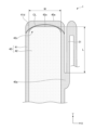
- FIG. 1 is a plan view illustrating a strain gauge according to a first embodiment.
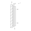
- FIG. 2 is a cross-sectional view illustrating the strain gauge according to the first embodiment.
- FIG. 3 is a diagram illustrating a strain gauge of a comparative example.
- FIG. 4 is a diagram illustrating the strain gauge according to this embodiment.
- FIG. 5 is a cross-sectional view illustrating the strain gauge according to the first embodiment.
- FIG. 6 is a plan view illustrating the strain gauge according to the second embodiment.
- FIG. 7 is a plan view illustrating the strain gauge according to the third embodiment.
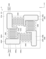
- FIG. 8 is a plan view illustrating the strain sensor according to the fourth embodiment.
- “approximately parallel” means that even if two lines or two surfaces are not completely parallel to each other, they can be treated as parallel to each other as long as it is within the range of manufacturing tolerance.
- “approximately parallel,” “approximately right angle,” “approximately perpendicular,” “approximately horizontal,” and “approximately vertical” are each intended to fall under the respective terms as long as the relative positions of the two lines or two surfaces are within the range of manufacturing tolerance.
- Fig. 1 is a plan view illustrating a strain gauge according to the first embodiment.
- Fig. 2 is a cross-sectional view illustrating a strain gauge according to the first embodiment.
- Fig. 2 is a cross-sectional view taken along line A-A in Fig. 1.
- an XY orthogonal coordinate system consisting of an X-axis and a Y-axis perpendicular to each other may be set in the drawings. Note that this coordinate system is defined for the purpose of explanation, and does not limit the attitude of the strain sensor and the like according to this embodiment.
- the strain gauge 1 has a substrate 10, a resistor 30, a pair of wirings 40 (first wiring and second wiring), and a pair of electrodes 50.
- the side of the substrate 10 on which the resistor 30 is provided is referred to as the upper side or one side, and the side on which the resistor 30 is not provided is referred to as the lower side or the other side.
- the surface on which the resistor 30 is provided in each portion is referred to as the one side or top side, and the surface on which the resistor 30 is not provided is referred to as the other side or bottom side.
- the strain gauge 1 can be used upside down or placed at any angle.
- a planar view refers to viewing the object from the normal direction of the top surface 10a of the substrate 10
- a planar shape refers to the shape of the object viewed from the normal direction of the top surface 10a of the substrate 10.
- the substrate 10 is a flexible member that serves as a base layer for forming the resistor 30 and the like.
- the thickness of the substrate 10 can be about 5 ⁇ m to 500 ⁇ m.
- a thickness of 5 ⁇ m to 200 ⁇ m is preferable in terms of the transmission of strain from the surface of the strain generator that is joined to the underside of the substrate 10 via an adhesive layer or the like, and dimensional stability against the environment, and a thickness of 10 ⁇ m or more is even more preferable in terms of insulation.
- the substrate 10 can be formed from an insulating resin film such as PI (polyimide) resin, epoxy resin, PEEK (polyether ether ketone) resin, PEN (polyethylene naphthalate) resin, PET (polyethylene terephthalate) resin, PPS (polyphenylene sulfide) resin, polyolefin resin, etc.
- PI polyimide
- epoxy resin epoxy resin
- PEEK polyether ether ketone
- PEN polyethylene naphthalate
- PET polyethylene terephthalate
- PPS polyphenylene sulfide
- the base material 10 may be formed from an insulating resin film that contains fillers such as silica or alumina.
- Examples of materials other than resin for the substrate 10 include crystalline materials such as SiO2 , ZrO2 (including YSZ), Si, Si2N3 , Al2O3 (including sapphire ), ZnO, perovskite ceramics ( CaTiO3 , BaTiO3 ), and amorphous glass.
- Metals such as aluminum, aluminum alloys (duralumin), and titanium may also be used as the material for the substrate 10. In this case, for example, an insulating film is formed on the metal substrate 10.
- the resistor 30 is a thin film formed in a predetermined pattern on the substrate 10, and is a sensing part that generates a resistance change when strained.
- the resistor 30 may be formed directly on the upper surface 10a of the substrate 10, or may be formed on the upper surface 10a of the substrate 10 via another layer. For convenience, the resistor 30 is shown in FIG. 1 with a dark matte pattern.
- the resistor 30 can be formed, for example, from a material containing Cr (chromium), a material containing Ni (nickel), or a material containing both Cr and Ni. That is, the resistor 30 can be formed from a material containing at least one of Cr and Ni.
- a material containing Cr is a Cr mixed phase film.
- An example of a material containing Ni is Cu-Ni (copper-nickel).
- An example of a material containing both Cr and Ni is Ni-Cr (nickel-chromium).
- the Cr mixed phase film is a film in which Cr, CrN, Cr 2 N, etc. are mixed together.
- the Cr mixed phase film may contain inevitable impurities such as chromium oxide.
- the thickness of the resistor 30 is not particularly limited and can be appropriately selected depending on the purpose.
- the thickness of the resistor 30 can be about 0.05 ⁇ m to 2 ⁇ m.
- a thickness of 0.1 ⁇ m or more is preferable in that the crystallinity of the crystals constituting the resistor 30 (for example, the crystallinity of ⁇ -Cr) is improved, and a thickness of 1 ⁇ m or less is even more preferable in that breakage of the film and warping from the substrate 10 caused by internal stress of the film constituting the resistor 30 can be reduced.
- the width of the resistor 30 can be optimized for the required specifications such as resistance value and lateral sensitivity, and can be about 10 ⁇ m to 100 ⁇ m, for example, taking into consideration measures against breakage.
- the stability of the gauge characteristics can be improved by making ⁇ -Cr (alpha chromium), which is a stable crystal phase, the main component.
- the gauge factor of strain gauge 1 can be set to 10 or more, and the gauge factor temperature coefficient TCS and the temperature coefficient of resistance TCR can be set within the range of -1000 ppm/°C to +1000 ppm/°C.
- main component means that the target substance accounts for 50% by weight or more of the total substance that constitutes the resistor.
- resistor 30 preferably contains 80% by weight or more of ⁇ -Cr, and even more preferably contains 90% by weight or more.
- ⁇ -Cr is Cr with a bcc structure (body-centered cubic lattice structure).
- the Cr mixed-phase film preferably contains 20% by weight or less of CrN and Cr 2 N.
- the Cr mixed-phase film preferably contains 20% by weight or less of CrN and Cr 2 N.
- the ratio of Cr2N in CrN and Cr2N is preferably 80% by weight or more and less than 90% by weight, and more preferably 90% by weight or more and less than 95% by weight.
- the ratio of Cr2N in CrN and Cr2N is 90% by weight or more and less than 95% by weight, the decrease in TCR (negative TCR) becomes more significant due to the Cr2N having semiconductor properties.
- the ceramicization by reducing the ceramicization, brittle fracture is reduced.
- the ends of the two elongated portions 31 located at both ends of the resistor 30 are bent toward the adjacent wiring 40 (the X-axis direction in the example of FIG. 1). These bent ends (hereinafter also referred to simply as “resistor ends”) are made of the same material as the elongated portions 31, and are the portions from which the elongated portions 31 extend.
- each wiring 40 extends along the Y-axis direction.
- each wiring 40 has a longitudinal direction in the Y-axis direction.
- specific parts of the wiring 40 are named, but each part of the wiring 40 described below is formed integrally with each other.
- Each of the wirings 40 includes a side 40h, a side 40g, a terminal portion 40e, and a connection portion 40a.
- the side 40h indicates the side of the wiring 40 on which the resistor 30 is formed in a plan view.
- the side 40g indicates the side of the wiring 40 on which the resistor 30 is not formed in a plan view.
- the terminal portion 40e indicates the terminal portion of the wiring 40 on the opposite side to the side connected to the electrode 50 (the positive Y-axis side in the example of FIG. 1).
- At least one of the pair of wirings 40 has a connection portion 40a on the side 40h at a position separated from the terminal portion 40e. In the example of FIG. 1, both of the two wirings 40 have a connection portion 40a at a position separated from the terminal portion 40e.
- the connection portion 40a is connected to the end of the resistor 30.
- the second metal layer 42 and the second metal layer 52 may be formed from a material having a lower resistance than the resistor 30 (as well as the first metal layer 41 and the first metal layer 51).
- the material of the second metal layer 42 and the second metal layer 52 can be Cu, Ni, Al, Ag, Au, Pt, etc., or an alloy of any of these metals, a compound of any of these metals, or a laminated film in which any of these metals, alloys, and compounds are appropriately laminated.
- the thickness of the second metal layer 42 and the second metal layer 52 can be about 3 ⁇ m to 5 ⁇ m.
- the second metal layer 42 may be formed on a part of the first metal layer 41 or on the entire first metal layer 41.
- the second metal layer 52 may be formed on a part of the first metal layer 51 or on the entire first metal layer 51.
- One or more other metal layers may be laminated on the upper surface of the second metal layer 52.
- the second metal layer 52 may be a copper layer, and a gold layer may be laminated on the upper surface of the copper layer.
- the second metal layer 52 may be a copper layer, and a palladium layer and a gold layer may be sequentially laminated on the upper surface of the copper layer.
- a cover layer may be provided on the upper surface 10a of the substrate 10 to cover the resistor 30 and the wiring 40 and expose the electrodes 50. By providing a cover layer, mechanical damage to the resistor 30 and the wiring 40 can be prevented. Furthermore, by providing a cover layer, the resistor 30 and the wiring 40 can be protected from moisture and the like.
- the cover layer may be provided so as to cover the entire portion except for the electrodes 50.
- the cover layer can be formed from an insulating resin such as PI resin, epoxy resin, PEEK resin, PEN resin, PET resin, PPS resin, or composite resin (e.g., silicone resin, polyolefin resin).
- the cover layer may contain a filler or pigment.
- the thickness of the cover layer can be about 2 ⁇ m to 30 ⁇ m.
- the wiring 40 has a structure in which the second metal layer 42 is laminated on the first metal layer 41 made of the same material as the resistor 30. Therefore, the resistance of each wiring 40 is lower than that of the resistor 30, and it is possible to prevent each wiring 40 from functioning as a resistor. As a result, it is possible to improve the accuracy of strain detection by the resistor 30.
- strain gauge 1 by providing wiring 40 with a lower resistance than resistor 30, the actual sensing area of strain gauge 1 can be limited to the local area where resistor 30 is formed. This improves the accuracy of strain detection by resistor 30.
- making the wiring 40 less resistant than the resistor 30 and limiting the actual sensing area to the local area where the resistor 30 is formed has a significant effect on improving strain detection accuracy. Furthermore, making the wiring 40 less resistant than the resistor 30 also has the effect of reducing lateral sensitivity.
- FIG. 3 is a diagram explaining strain gauge 1z of the comparative example. Note that FIG. 3 shows an enlarged view of the vicinity of the end of the wiring. Strain gauge 1z has the same configuration as strain gauge 1 shown in FIGS. 1 and 2, except that the connection position between the resistor and the wiring is different from that of strain gauge 1, and the shape of the wiring is different from that of strain gauge 1.
- the wiring is connected to the resistor near the end.
- the connection part of the wiring and/or resistor may break, for example as shown in Figure 3.
- the distance L between the connection portion 40a and the terminal end 42e may be 30 micrometers or more. By making the distance L 30 micrometers or more, the above-mentioned breakage can be suppressed with a higher probability.
- the wiring 40 is connected to the resistor 30 at a position 30 micrometers or more away from the terminal end 42e of the second metal layer 42.
- the width W of the edge at the terminal portion 42e of the second metal layer 42 is wider than that of the comparative example.
- this width W is 50 micrometers or more in a plan view. Disconnections often occur at narrowed portions of the peripheral ends of the wiring, power supply, resistor, etc. of the strain gauge. Therefore, by widening the width W, it is possible to suppress the occurrence of disconnections.
- at least one of the corners 42c of the second metal layer 42 may be formed as a right angle or an obtuse angle in a plan view.
- a substrate 10 is prepared, and a metal layer (for convenience, referred to as metal layer A) is formed on the upper surface 10a of the substrate 10.
- Metal layer A is a layer that is ultimately patterned to become resistor 30, first metal layer 41, and first metal layer 51. Therefore, the material and thickness of metal layer A are the same as those of resistor 30, first metal layer 41, and first metal layer 51 described above.
- the metal layer A can be formed, for example, by magnetron sputtering using a raw material capable of forming the metal layer A as a target.
- the metal layer A may also be formed by reactive sputtering, vapor deposition, arc ion plating, pulsed laser deposition, or the like.
- a functional layer of a predetermined thickness may be vacuum-deposited as a base layer on the upper surface 10a of the substrate 10 by, for example, a conventional sputtering method before depositing the metal layer A.
- the functional layer refers to a layer that has the function of promoting the crystal growth of at least the upper layer, metal layer A (resistor 30).
- the functional layer preferably also has the function of preventing oxidation of metal layer A due to oxygen and moisture contained in the substrate 10, and the function of improving adhesion between the substrate 10 and metal layer A.
- the functional layer may also have other functions.
- the insulating resin film that constitutes the substrate 10 contains oxygen and moisture, and since Cr forms a self-oxidizing film, particularly when the metal layer A contains Cr, it is effective for the functional layer to have the function of preventing oxidation of the metal layer A.
- the material of the functional layer may be one or more metals selected from the group consisting of Cr (chromium), Ti (titanium), V (vanadium), Nb (niobium), Ta (tantalum), Ni (nickel), Y (yttrium), Zr (zirconium), Hf (hafnium), Si (silicon), C (carbon), Zn (zinc), Cu (copper), Bi (bismuth), Fe (iron), Mo (molybdenum), W (tungsten), Ru (ruthenium), Rh (rhodium), Re (rhenium), Os (osmium), Ir (iridium), Pt (platinum), Pd (palladium), Ag (silver), Au (gold), Co (cobalt), Mn (manganese), and Al
- Examples of the alloy include FeCr, TiAl, FeNi, NiCr, CrCu, etc.
- Examples of the compound include TiN, TaN , Si3N4 , TiO2 , Ta2O5 , SiO2 , etc.
- the thickness of the functional layer is preferably 1/20 or less of the thickness of the resistor. In this range, the crystal growth of ⁇ -Cr can be promoted, and a part of the current flowing through the resistor can be prevented from flowing through the functional layer, which would reduce the sensitivity of strain detection.
- the thickness of the functional layer is 1/50 or less of the thickness of the resistor. In this range, the crystal growth of ⁇ -Cr can be promoted, and it is also possible to further prevent a portion of the current flowing through the resistor from flowing through the functional layer, thereby reducing the sensitivity of strain detection.
- the functional layer is made of a conductive material such as a metal or alloy, it is even more preferable that the thickness of the functional layer is 1/100 or less of the thickness of the resistor. In this range, it is possible to further prevent a portion of the current flowing through the resistor from flowing through the functional layer, thereby reducing the strain detection sensitivity.
- the thickness of the functional layer is preferably 1 nm to 1 ⁇ m. This range promotes the crystal growth of ⁇ -Cr and allows the functional layer to be easily formed without cracking.
- the thickness of the functional layer is between 1 nm and 0.8 ⁇ m. This range not only promotes the crystal growth of ⁇ -Cr, but also makes it easier to form the functional layer without cracking it.
- the thickness of the functional layer is between 1 nm and 0.5 ⁇ m. This range promotes the crystal growth of ⁇ -Cr and makes it easier to form the functional layer without cracking.
- the planar shape of the functional layer is patterned, for example, to be substantially the same as the planar shape of the resistor shown in FIG. 1.
- the planar shape of the functional layer is not limited to being substantially the same as the planar shape of the resistor. If the functional layer is formed from an insulating material, it does not have to be patterned to be the same as the planar shape of the resistor.
- the functional layer may be formed in a solid shape at least in the area where the resistor is formed. Alternatively, the functional layer may be formed in a solid shape over the entire top surface of the substrate 10.
- the functional layer is made of an insulating material
- the functional layer is formed relatively thick, at a thickness of 50 nm to 1 ⁇ m, and formed in a solid shape, thereby increasing the thickness and surface area of the functional layer, and therefore heat generated by the resistor can be dissipated to the substrate 10.
- the deterioration of measurement accuracy due to self-heating of the resistor can be suppressed in the strain gauge 1.
- the functional layer can be formed in a vacuum by conventional sputtering, for example, using a raw material capable of forming the functional layer as a target and introducing Ar (argon) gas into a chamber.
- Ar argon
- the functional layer is formed while etching the upper surface 10a of the substrate 10 with Ar, so that the amount of functional layer formed can be minimized and adhesion can be improved.
- the functional layer may be formed by other methods.
- a method may be used in which the upper surface 10a of the substrate 10 is activated by a plasma treatment using Ar or the like before forming the functional layer, thereby improving adhesion, and then the functional layer is vacuum-formed by magnetron sputtering.
- the material of the functional layer and the material of the metal layer A there are no particular restrictions on the combination of the material of the functional layer and the material of the metal layer A, and they can be selected appropriately depending on the purpose.
- the metal layer A can be formed by magnetron sputtering using a raw material capable of forming a Cr mixed phase film as a target and introducing Ar gas into a chamber.
- the metal layer A can be formed by reactive sputtering using pure Cr as a target and introducing an appropriate amount of nitrogen gas together with Ar gas into a chamber.
- the ratio of CrN and Cr 2 N contained in the Cr mixed phase film and the ratio of Cr 2 N in CrN and Cr 2 N can be adjusted by changing the amount and pressure (nitrogen partial pressure) of the nitrogen gas introduced or by adjusting the heating temperature by providing a heating process.
- the growth surface of the Cr mixed-phase film is determined by the functional layer made of Ti, and a Cr mixed-phase film can be formed that is mainly composed of ⁇ -Cr, which has a stable crystal structure. Furthermore, the Ti that constitutes the functional layer diffuses into the Cr mixed-phase film, improving the gauge characteristics.
- the gauge factor of the strain gauge 1 can be set to 10 or more, and the gauge factor temperature coefficient TCS and the resistance temperature coefficient TCR can be set within the range of -1000 ppm/°C to +1000 ppm/°C.
- the Cr mixed-phase film may contain Ti and TiN (titanium nitride).
- the functional layer made of Ti has all of the following functions: promoting crystal growth of metal layer A, preventing oxidation of metal layer A due to oxygen and moisture contained in substrate 10, and improving adhesion between substrate 10 and metal layer A.
- Ta, Si, Al, or Fe is used as the functional layer instead of Ti.
- the second metal layer 42 and the second metal layer 52 are formed on the upper surface of the metal layer A.
- the second metal layer 42 and the second metal layer 52 can be formed, for example, by a photolithography method.
- a seed layer is formed by, for example, sputtering or electroless plating so as to cover the upper surface of metal layer A.
- a photosensitive resist is formed over the entire upper surface of the seed layer, and is exposed and developed to form openings that expose the areas in which second metal layer 42 and second metal layer 52 will be formed.
- second metal layer 42 and second metal layer 52 can be formed into any shape.
- a dry film resist can be used as the resist.
- the second metal layer 42 and the second metal layer 52 are formed on the seed layer exposed in the opening, for example, by electrolytic plating using the seed layer as the power supply path.
- the electrolytic plating method is advantageous in that it has high tact and can form low-stress electrolytic plating layers as the second metal layer 42 and the second metal layer 52. By making the thick electrolytic plating layer low-stress, it is possible to prevent warping of the strain gauge 1.
- the second metal layer 42 and the second metal layer 52 may also be formed by electroless plating.
- the resist is removed.
- the resist can be removed, for example, by immersing it in a solution that can dissolve the resist material.
- a photosensitive resist is formed on the entire upper surface of the seed layer, and is exposed and developed to pattern the resist 30, wiring 40, and electrode 50 in the same planar shape as those in FIG. 1.
- a dry film resist can be used as the resist.
- the resist is used as an etching mask to remove the metal layer A and the seed layer exposed from the resist, and the resist 30, wiring 40, and electrode 50 in the planar shape of FIG. 1 are formed.
- metal layer A and the seed layer can be removed by wet etching. If a functional layer is formed below metal layer A, the functional layer is patterned by etching into the planar shape shown in FIG. 1, similar to resistor 30, wiring 40, and electrode 50. At this point, a seed layer is formed on resistor 30, first metal layer 41, and first metal layer 51.
- the second metal layer 42 and the second metal layer 52 are used as an etching mask to remove the unnecessary seed layer exposed from the second metal layer 42 and the second metal layer 52, thereby forming the second metal layer 42 and the second metal layer 52.
- the seed layer directly below the second metal layer 42 and the second metal layer 52 remains.
- the unnecessary seed layer can be removed by wet etching using an etching solution that etches the seed layer but does not etch the functional layer, resistor 30, wiring 40, and electrode 50.
- a cover layer that covers the resistor 30 and wiring 40 and exposes the electrodes 50 is provided on the upper surface 10a of the substrate 10, completing the strain gauge 1.
- the cover layer can be produced, for example, by laminating a semi-cured thermosetting insulating resin film on the upper surface 10a of the substrate 10 so as to cover the resistor 30 and wiring 40 and expose the electrodes 50, and then heating and hardening the film.
- the cover layer can also be produced by applying a liquid or paste-like thermosetting insulating resin to the upper surface 10a of the substrate 10 so as to cover the resistor 30 and wiring 40 and expose the electrodes 50, and then heating and hardening the resin.
- the opening that exposes the electrodes 50 can be formed, for example, by photolithography.
- the strain gauge 2 has a substrate 110, a resistor 130, wiring 40, and electrodes 50.
- the resistor 130 and wiring 40 are formed on the surface 110a of the substrate 110.
- the explanation of the substrate 110 is omitted here and the explanation of the substrate 110 should be referred to the explanation of the substrate 10.
- the explanation of the wiring 40 and the electrodes 50 is omitted here and the explanation of the wiring 40 and the electrodes 50 should be referred to the explanation of the first embodiment.
- the resistor 130 includes a first sensing portion 131, a second sensing portion 132, and a joint portion 133.
- the first sensing portion 131 has a structure in which a plurality of elongated portions 31 are arranged at predetermined intervals with their longitudinal direction facing the same direction (Y-axis direction), and the ends of adjacent elongated portions 31 are alternately connected to form a zigzag fold as a whole.
- One end 131e1 of the first sensing portion 131 is electrically connected to the electrode 50 via the wiring 40.
- the end 131e1 is also connected to the wiring 40 at the connection portion 40a. As shown in the figure, the connection portion 40a is spaced from the end portion 40e of the wiring 40.
- the other end 131e2 of the first sensing portion 131 is electrically connected to the joint portion 133.
- the second sensing part 132 has the same configuration as the first sensing part. That is, the second sensing part 132 has a structure in which a plurality of elongated parts 31 are arranged at a predetermined interval with their longitudinal direction facing the same direction (Y-axis direction), and the ends of adjacent elongated parts 31 are alternately connected to form a zigzag fold as a whole.
- One end 132e1 of the second sensing part 132 is electrically connected to the electrode 50 via the wiring 40.
- this end 132e1 is connected to the wiring 40 at the connection part 40a, and the connection part 40a is separated from the terminal part 40e of the wiring 40.
- the other end 132e2 of the second sensing part 132 is electrically connected to the joint part 133.
- the joint 133 is disposed between the first sensing portion 131 and the second sensing portion 132.
- the joint 133 is a member made of the same material as the wiring 40.
- the joint 133 may be formed on the substrate 110 in the same manner as the wiring 40. Furthermore, the shape and size of the joint 133 are not particularly limited.
- the joint 133 may be connected to an end of the first sensing portion 131 and/or an end of the second sensing portion 132 (i.e., end 131e2 and/or end 132e2) at a position spaced apart from each of the end portions 133e and 133f.
- the strain gauge 2 has two sensing parts.
- the number of sensing parts is not limited to two, and it may have three or more sensing parts.
- the resistor has three or more sensing parts connected in series as a whole, and a joint is provided between each of the three or more sensing parts.
- the resistor 130 is connected to the wiring 40 at a position away from the terminal end 40e. Therefore, for the same reasons as the strain gauge 1, the strain gauge 2 can be said to be a strain gauge that is less likely to break. Furthermore, in the strain gauge 2, the sensing part (first sensing part 131 and/or second sensing part 132) of the resistor 130 is connected to the joint 133 at a position away from the terminal end 133e and the terminal end 133f of the joint 133. Therefore, according to the strain gauge 2, it is possible to realize a strain gauge that is less likely to break even near the joint 133 (for example, at the corners of the terminal end of the joint 133).
- FIG. 7 is a plan view illustrating a strain gauge 3 according to the third embodiment.
- the strain gauge 3 differs from the strain gauge 1 in that the strain gauge 3 has a third metal layer 90 arranged around the resistor 30 and spaced apart from the resistor 30, the wiring 40, and the electrode 50.
- the third metal layer 90 is formed from the same material as the resistor 30.
- the third metal layer 90 can be formed in the same process as the resistor 30 and the first metal layer 41. It is preferable to arrange the third metal layer 90 in the excess space around the resistor 30 so that it has as large an area as possible.
- a metal layer made of the same material as the second metal layer 42, etc. may be laminated on the third metal layer 90.
- the rigidity of the strain gauge 3 can be made even higher than that of the strain gauge 1. By increasing the rigidity of the strain gauge 3, breakage of the strain gauge 3 can be suppressed.
- the strain gauge according to the third embodiment makes it possible to reduce the likelihood of breakage of the strain gauge even when stress is concentrated around the wiring end and the resistor (for example, near the joint 133). Furthermore, the strain gauge according to the third embodiment is provided with a third metal layer, which increases the rigidity of the strain gauge and thereby reduces breakage of the strain gauge 3.
- the fourth embodiment an example of a strain sensor including a plurality of strain gauges will be described.
- the plurality of strain gauges are connected to each other by sharing at least one of their electrodes and at least one of their wirings to form a bridge circuit.
- FIG. 8 is a plan view illustrating a strain sensor 4 according to the fourth embodiment.
- the strain sensor 4 includes a substrate 210, resistors 230A, 230B, 230C, and 230D, and wiring 240A, 240B, 240C, and 240D.
- Resistors 230A, 230B, 230C, and 230D, wiring 240A, 240B, 240C, and 240D are formed on a surface 210a of the substrate 210.
- Each of the wiring 240A and the wiring 240C extends along the Y-axis direction. In other words, each of the wiring 240A and the wiring 240C has a longitudinal direction in the Y-axis direction.
- Each of the wiring 240B and the wiring 240D extends along the X-axis direction. In other words, each of the wiring 240B and the wiring 240D has a longitudinal direction in the X-axis direction.
- the electrodes of the strain sensor 4 are not explicitly shown, but in the example of the figure, part of the wiring acts as the electrodes of the strain sensor 4.
- Each of resistors 230A, 230B, 230C, and 230D may be formed of the same material as resistor 30 according to the first embodiment.
- wiring 240A, 240B, 240C, and 240D may be formed of the same material as wiring 40 according to the first embodiment.
- Resistor 230A is connected to wiring 240A and wiring 240B.
- Resistor 230B is connected to wiring 240B and wiring 240C.
- Resistor 230C is connected to wiring 240C and wiring 240D.
- Resistor 230D is connected to wiring 240D and wiring 240A.
- Wiring 240A has a first metal layer 241A and a second metal layer 242A laminated on the upper surface of the first metal layer 241A.
- Wiring 240B has a first metal layer 241B and a second metal layer 242B laminated on the upper surface of the first metal layer 241B.
- Wiring 240C has a first metal layer 241C and a second metal layer 242C laminated on the upper surface of the first metal layer 241C.
- Wiring 240D has a first metal layer 241D and a second metal layer 242D laminated on the upper surface of the first metal layer 241D.
- First metal layer 241A, first metal layer 241B, first metal layer 241C, and first metal layer 241D may be formed of the same material as first metal layer 41. Also, second metal layer 242A, second metal layer 242B, second metal layer 242C, and second metal layer 242D may be formed of the same material as second metal layer 42.
- wiring 240B, wiring 240C, and wiring 240D are different, their shapes and connection relationships with the resistor are similar to those of wiring 240A. Therefore, below, the connection between each wiring and the resistor according to the fourth embodiment will be described using wiring 240A.
- Wiring 240A has a generally L-shape in plan view.
- Wiring 240A has, in order from end 240Ae, side 240Ai, end 240Aj, side 240Ah, end 240Af, and side 240Ag.
- Resistor 230A is connected to end 240Ae.
- the position to which resistor 230A is connected is a position at end 240Ae that is spaced apart from each of side portions 240Ag and 240Ai.
- Resistor 230D is connected to side portion 240Ah.
- the position to which resistor 230D is connected is a position at side portion 240Ah that is spaced apart from each of end portions 240Aj and 240Af.
- wiring 240A shares at least one of the electrodes of each of the multiple strain gauges, and at least one of the wiring and the second wiring, providing an example of a configuration in which electrodes, wiring, and at least one of the wiring are shared.
- the strain gauge according to the fourth embodiment can suppress the occurrence of breakage.
- the strain sensor according to the fourth embodiment can make it difficult for breakage to occur in the strain gauge even when stress is concentrated at the end of the wiring.
Landscapes
- Physics & Mathematics (AREA)
- General Physics & Mathematics (AREA)
- Measurement Of Length, Angles, Or The Like Using Electric Or Magnetic Means (AREA)
Priority Applications (2)
| Application Number | Priority Date | Filing Date | Title |
|---|---|---|---|
| CN202480014711.6A CN120752492A (zh) | 2023-02-27 | 2024-02-21 | 应变计及应变传感器 |
| EP24763752.3A EP4675221A1 (en) | 2023-02-27 | 2024-02-21 | Strain gauge and strain sensor |
Applications Claiming Priority (2)
| Application Number | Priority Date | Filing Date | Title |
|---|---|---|---|
| JP2023028342A JP2024121310A (ja) | 2023-02-27 | 2023-02-27 | ひずみゲージおよびひずみセンサ |
| JP2023-028342 | 2023-02-27 |
Publications (1)
| Publication Number | Publication Date |
|---|---|
| WO2024181271A1 true WO2024181271A1 (ja) | 2024-09-06 |
Family
ID=92590605
Family Applications (1)
| Application Number | Title | Priority Date | Filing Date |
|---|---|---|---|
| PCT/JP2024/006296 Ceased WO2024181271A1 (ja) | 2023-02-27 | 2024-02-21 | ひずみゲージおよびひずみセンサ |
Country Status (4)
| Country | Link |
|---|---|
| EP (1) | EP4675221A1 (https=) |
| JP (1) | JP2024121310A (https=) |
| CN (1) | CN120752492A (https=) |
| WO (1) | WO2024181271A1 (https=) |
Citations (6)
| Publication number | Priority date | Publication date | Assignee | Title |
|---|---|---|---|---|
| JP3040684U (ja) * | 1997-02-18 | 1997-08-26 | 株式会社共和電業 | ひずみゲージ |
| JP2009302117A (ja) * | 2008-06-10 | 2009-12-24 | Minebea Co Ltd | タブパターンとリードの接合方法 |
| JP2017150931A (ja) * | 2016-02-24 | 2017-08-31 | 株式会社タニタ | ひずみゲージ |
| JP2022008026A (ja) | 2020-04-08 | 2022-01-13 | ミネベアミツミ株式会社 | ひずみゲージ |
| JP2022189613A (ja) * | 2021-06-11 | 2022-12-22 | ミネベアミツミ株式会社 | ひずみゲージ |
| JP2023028342A (ja) | 2021-08-19 | 2023-03-03 | 富士電機株式会社 | 洗浄装置 |
-
2023
- 2023-02-27 JP JP2023028342A patent/JP2024121310A/ja active Pending
-
2024
- 2024-02-21 CN CN202480014711.6A patent/CN120752492A/zh active Pending
- 2024-02-21 EP EP24763752.3A patent/EP4675221A1/en active Pending
- 2024-02-21 WO PCT/JP2024/006296 patent/WO2024181271A1/ja not_active Ceased
Patent Citations (6)
| Publication number | Priority date | Publication date | Assignee | Title |
|---|---|---|---|---|
| JP3040684U (ja) * | 1997-02-18 | 1997-08-26 | 株式会社共和電業 | ひずみゲージ |
| JP2009302117A (ja) * | 2008-06-10 | 2009-12-24 | Minebea Co Ltd | タブパターンとリードの接合方法 |
| JP2017150931A (ja) * | 2016-02-24 | 2017-08-31 | 株式会社タニタ | ひずみゲージ |
| JP2022008026A (ja) | 2020-04-08 | 2022-01-13 | ミネベアミツミ株式会社 | ひずみゲージ |
| JP2022189613A (ja) * | 2021-06-11 | 2022-12-22 | ミネベアミツミ株式会社 | ひずみゲージ |
| JP2023028342A (ja) | 2021-08-19 | 2023-03-03 | 富士電機株式会社 | 洗浄装置 |
Non-Patent Citations (1)
| Title |
|---|
| See also references of EP4675221A1 |
Also Published As
| Publication number | Publication date |
|---|---|
| EP4675221A1 (en) | 2026-01-07 |
| JP2024121310A (ja) | 2024-09-06 |
| CN120752492A (zh) | 2025-10-03 |
Similar Documents
| Publication | Publication Date | Title |
|---|---|---|
| JP7764650B2 (ja) | ひずみゲージ | |
| JP7570975B2 (ja) | ひずみゲージ | |
| US11499877B2 (en) | Strain gauge | |
| US20200292294A1 (en) | Strain gauge and sensor module | |
| US12379268B2 (en) | Strain gauge | |
| JP7789492B2 (ja) | 脈波センサ | |
| JP7383656B2 (ja) | ひずみゲージ | |
| US11300398B2 (en) | Strain gauge with improved distortion of measured object | |
| JP2019132791A (ja) | ひずみゲージ | |
| WO2021205981A1 (ja) | ひずみゲージ | |
| JP2025170444A (ja) | ひずみ検出システム | |
| JP7737790B2 (ja) | ひずみゲージ | |
| JP7469933B2 (ja) | ひずみゲージ | |
| JP7697758B2 (ja) | ひずみゲージ | |
| WO2024181271A1 (ja) | ひずみゲージおよびひずみセンサ | |
| JP2022008026A (ja) | ひずみゲージ | |
| JP7605414B2 (ja) | ひずみゲージ | |
| JP7577908B2 (ja) | ひずみゲージ | |
| JP7658050B2 (ja) | ひずみゲージ、センサモジュール、及び起歪体 | |
| JP7577907B2 (ja) | ひずみゲージ | |
| JP2024136860A (ja) | ひずみゲージおよびひずみセンサ | |
| US20250172444A1 (en) | Strain gauge | |
| JP2025139871A (ja) | ひずみゲージ | |
| JP2024088419A (ja) | ひずみゲージ | |
| WO2022124238A1 (ja) | ひずみゲージ |
Legal Events
| Date | Code | Title | Description |
|---|---|---|---|
| 121 | Ep: the epo has been informed by wipo that ep was designated in this application |
Ref document number: 24763752 Country of ref document: EP Kind code of ref document: A1 |
|
| WWE | Wipo information: entry into national phase |
Ref document number: 202480014711.6 Country of ref document: CN |
|
| WWE | Wipo information: entry into national phase |
Ref document number: 2024763752 Country of ref document: EP |
|
| NENP | Non-entry into the national phase |
Ref country code: DE |
|
| WWP | Wipo information: published in national office |
Ref document number: 202480014711.6 Country of ref document: CN |
|
| ENP | Entry into the national phase |
Ref document number: 2024763752 Country of ref document: EP Effective date: 20250929 |
|
| ENP | Entry into the national phase |
Ref document number: 2024763752 Country of ref document: EP Effective date: 20250929 |
|
| ENP | Entry into the national phase |
Ref document number: 2024763752 Country of ref document: EP Effective date: 20250929 |
|
| WWP | Wipo information: published in national office |
Ref document number: 2024763752 Country of ref document: EP |