WO2024176756A1 - 電子装置 - Google Patents
電子装置 Download PDFInfo
- Publication number
- WO2024176756A1 WO2024176756A1 PCT/JP2024/003013 JP2024003013W WO2024176756A1 WO 2024176756 A1 WO2024176756 A1 WO 2024176756A1 JP 2024003013 W JP2024003013 W JP 2024003013W WO 2024176756 A1 WO2024176756 A1 WO 2024176756A1
- Authority
- WO
- WIPO (PCT)
- Prior art keywords
- electronic device
- thickness direction
- wiring
- joint
- viewed
- Prior art date
- Legal status (The legal status is an assumption and is not a legal conclusion. Google has not performed a legal analysis and makes no representation as to the accuracy of the status listed.)
- Ceased
Links
Images












Classifications
-
- H—ELECTRICITY
- H05—ELECTRIC TECHNIQUES NOT OTHERWISE PROVIDED FOR
- H05K—PRINTED CIRCUITS; CASINGS OR CONSTRUCTIONAL DETAILS OF ELECTRIC APPARATUS; MANUFACTURE OF ASSEMBLAGES OF ELECTRICAL COMPONENTS
- H05K1/00—Printed circuits
- H05K1/02—Details
-
- H—ELECTRICITY
- H05—ELECTRIC TECHNIQUES NOT OTHERWISE PROVIDED FOR
- H05K—PRINTED CIRCUITS; CASINGS OR CONSTRUCTIONAL DETAILS OF ELECTRIC APPARATUS; MANUFACTURE OF ASSEMBLAGES OF ELECTRICAL COMPONENTS
- H05K1/00—Printed circuits
- H05K1/18—Printed circuits structurally associated with non-printed electric components
-
- H—ELECTRICITY
- H05—ELECTRIC TECHNIQUES NOT OTHERWISE PROVIDED FOR
- H05K—PRINTED CIRCUITS; CASINGS OR CONSTRUCTIONAL DETAILS OF ELECTRIC APPARATUS; MANUFACTURE OF ASSEMBLAGES OF ELECTRICAL COMPONENTS
- H05K3/00—Apparatus or processes for manufacturing printed circuits
- H05K3/30—Assembling printed circuits with electric components, e.g. with resistors
- H05K3/32—Assembling printed circuits with electric components, e.g. with resistors electrically connecting electric components or wires to printed circuits
- H05K3/34—Assembling printed circuits with electric components, e.g. with resistors electrically connecting electric components or wires to printed circuits by soldering
-
- H—ELECTRICITY
- H10—SEMICONDUCTOR DEVICES; ELECTRIC SOLID-STATE DEVICES NOT OTHERWISE PROVIDED FOR
- H10W—GENERIC PACKAGES, INTERCONNECTIONS, CONNECTORS OR OTHER CONSTRUCTIONAL DETAILS OF DEVICES COVERED BY CLASS H10
- H10W70/00—Package substrates; Interposers; Redistribution layers [RDL]
- H10W70/60—Insulating or insulated package substrates; Interposers; Redistribution layers
Definitions
- This disclosure relates to electronic devices.
- Patent Document 1 discloses an example of a conventional electronic device.
- the electronic device (semiconductor device) described in Patent Document 1 has an insulating layer, a wiring layer, multiple bonding layers, and multiple electronic components.
- the wiring layer is disposed on the insulating layer.
- the wiring layer constitutes the position of the conduction path between the multiple electronic components and the semiconductor device described in Patent Document 1.
- Each of the multiple electronic components is either a resistor, a passive element such as a capacitor or an inductor, or a diode.
- the multiple electronic components are surface-mounted and chip-type.
- Each of the multiple electronic components has an electrode. In each electronic component, the electrode is bonded to the wiring layer via a bonding layer.
- defects in the bonding layer can lead to a decrease in the bonding strength between the electronic component and the wiring layer, and a decrease in the electrical conductivity between the electronic component and the wiring layer. Such a decrease in bonding strength and electrical conductivity reduces the reliability of the electronic device.
- An object of the present disclosure is to provide an electronic device that is an improvement over conventional devices.
- an object of the present disclosure is to provide an electronic device that can suppress a decrease in reliability.
- the electronic device provided by the first aspect of the present disclosure comprises a first electronic component having a first electrode, a first wiring portion conductive to the first electrode, and a first joint portion joining the first electrode and the first wiring portion.
- the first wiring portion has a first surface and a second surface each facing one side in the thickness direction of the first wiring portion.
- the first joint portion overlaps the first surface when viewed in the thickness direction.
- the second surface is located on one side of the thickness direction relative to the first surface, and is disposed on at least a portion of the periphery of the first surface when viewed in the thickness direction.
- the above configuration makes it possible to prevent a decrease in reliability in electronic devices.
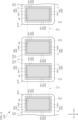
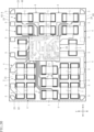
- FIG. 1 is a plan view showing an electronic device according to a first embodiment.
- FIG. 2 is a plan view of FIG. 1, in which the sealing resin is shown by imaginary lines.
- FIG. 3 is a plan view of FIG. 2 with the sealing resin omitted and a plurality of electronic components shown by imaginary lines.
- FIG. 4 is an enlarged view of a main portion of the plan view of FIG. 3, with a part of the plan view being enlarged and with a plurality of joints indicated by imaginary lines.
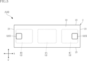
- FIG. 5 is a bottom view of the electronic device according to the first embodiment.
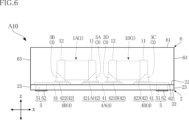
- FIG. 6 is a front view of the electronic device according to the first embodiment.
- FIG. 7 is a left side view showing the electronic device according to the first embodiment.
- FIG. 1 is a plan view showing an electronic device according to a first embodiment.
- FIG. 2 is a plan view of FIG. 1, in which the sealing resin is shown by imaginary lines.
- FIG. 3 is a plan view of FIG. 2 with the sealing resin omitted and
- FIG. 8 is a cross-sectional view taken along line VIII-VIII in FIG.
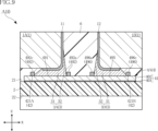
- FIG. 9 is an enlarged cross-sectional view of a main part of FIG.
- FIG. 10 is a cross-sectional view showing a step of the method for manufacturing an electronic device according to the first embodiment, and corresponds to the cross section of FIG.
- FIG. 11 is a cross-sectional view showing a step of the method for manufacturing an electronic device according to the first embodiment, and corresponds to the cross section of FIG.
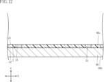
- FIG. 12 is a cross-sectional view showing a step of the method for manufacturing an electronic device according to the first embodiment, and corresponds to the cross section of FIG. FIG.
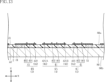
- FIG. 13 is a cross-sectional view showing a step of the method for manufacturing an electronic device according to the first embodiment, and corresponds to the cross section of FIG.
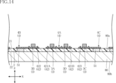
- FIG. 14 is a cross-sectional view showing a step of the method for manufacturing an electronic device according to the first embodiment, and corresponds to the cross section of FIG.
- FIG. 15 is a cross-sectional view showing a step of the method for manufacturing an electronic device according to the first embodiment, and corresponds to the cross section of FIG.
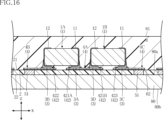
- FIG. 16 is a cross-sectional view showing a step of the method for manufacturing an electronic device according to the first embodiment, and corresponds to the cross section of FIG. FIG.
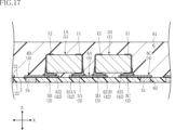
- FIG. 17 is a cross-sectional view showing a step of the method for manufacturing an electronic device according to the first embodiment, and corresponds to the cross section of FIG.
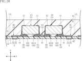
- FIG. 18 is a cross-sectional view showing a step of the method for manufacturing an electronic device according to the first embodiment, and corresponds to the cross section of FIG.
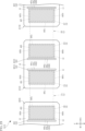
- FIG. 19 is an enlarged plan view of a main part showing an electronic device according to a first modified example of the first embodiment.
- FIG. 20 is an enlarged plan view of a main part showing an electronic device according to a second modified example of the first embodiment.
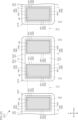
- FIG. 21 is an enlarged plan view of a main part of an electronic device according to a third modified example of the first embodiment.
- FIG. 22 is an enlarged plan view of a main portion showing another configuration example of an electronic device according to the third modified example of the first embodiment.
- FIG. 23 is an enlarged plan view of a main part of an electronic device according to a second embodiment, and corresponds to FIG.
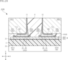
- FIG. 24 is an enlarged cross-sectional view of a main part of an electronic device according to the second embodiment, and corresponds to FIG.
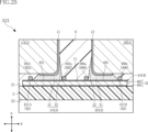
- FIG. 25 is an enlarged cross-sectional view of a main part showing an electronic device according to a modified example of the second embodiment, and corresponds to FIG.
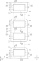
- FIG. 26 is an enlarged plan view of a main part of an electronic device according to a third embodiment, and corresponds to FIG.
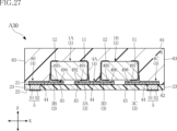
- FIG. 27 is a cross-sectional view showing an electronic device according to the third embodiment, and corresponds to FIG.
- FIG. 28 is an enlarged cross-sectional view of a main part of an electronic device according to the fourth embodiment, and corresponds to FIG.
- FIG. 29 is an enlarged plan view of a main portion showing another configuration example of an electronic device according to the present disclosure, and corresponds to FIG.
- FIG. 30 is a plan view showing another configuration example of the electronic device of the present disclosure, in which the sealing resin is indicated by imaginary lines.
- an object A is formed on an object B
- an object A is formed on (an object B)
- an object A is formed directly on an object B
- an object A is formed on an object B with another object interposed between the object A and the object B” unless otherwise specified.
- an object A is disposed on an object B” and “an object A is disposed on (an object B)” include “an object A is disposed directly on an object B” and “an object A is disposed on (an object B) with another object interposed between the object A and the object B” unless otherwise specified.
- an object A is located on (an object B) includes “an object A is in contact with an object B and is located on (an object B)” and “an object A is located on (an object B) with another object interposed between the object A and the object B".
- an object A overlaps an object B includes “an object A overlaps the entire object B” and “an object A overlaps a part of an object B” unless otherwise specified.
- An object A (a material) includes a certain material C includes “an object A (a material) is made of a certain material C” and "an object A (a material) is mainly composed of a certain material C”.
- a certain surface A faces a certain direction B includes, unless otherwise specified, the angle of the surface A with respect to the direction B is not limited to 90°, and includes the case where the surface A is inclined with respect to the direction B.
- An object A is perpendicular to an object B (a certain direction B) includes, unless otherwise specified, the angle of the object A with respect to the object B (a certain direction B) is not limited to the case where the angle is strictly 90°, and also includes the case where the angle is approximately 90° (for example, within the range of error caused by manufacturing variations).
- object A is parallel to object B (in a certain direction B) does not necessarily mean that object A is strictly parallel to object B (in a certain direction B), but also includes cases where object A is approximately parallel (for example, within the range of error caused by manufacturing variability).
- FIGS. 1 to 9 show an electronic device A10 according to a first embodiment.
- the electronic device A10 comprises a plurality of electronic components 1, a support member 2, a plurality of joints 3, a plurality of wiring sections 4, a plurality of terminals 5, and a sealing resin 6.
- the electronic device A10 is surface-mounted on a circuit board of an electrical product, an electric vehicle, or the like.
- the electronic device A10 is a leadless package type.
- the shape of the electronic device A10 in a plan view is, for example, rectangular.
- the thickness direction of the electronic device A10 is referred to as the "thickness direction z.”
- one side of the thickness direction z may be referred to as the upper side, and the other side as the lower side.
- the terms “upper,” “lower,” “upper,” “lower,” “top surface,” and “bottom surface” indicate the relative positional relationship of each component in the thickness direction z, and do not necessarily define the relationship with the direction of gravity.
- “Planar view” refers to the view in the thickness direction z.
- One direction perpendicular to the thickness direction z is referred to as the "first direction x.”
- the direction perpendicular to the thickness direction z and the first direction x is referred to as the "second direction y.”
- the multiple electronic components 1 are each supported by a support member 2, as shown in Figures 2 and 8.
- Each of the multiple electronic components 1 is an SMD (Surface Mount Device).
- Each of the multiple electronic components 1 is, for example, a resistor, a capacitor, an inductor, or a diode.
- the multiple electronic components 1 are functional elements of the electronic device A10.
- the multiple electronic components 1 include a first electronic component 1A and a second electronic component 1B. That is, the electronic device A10 includes a first electronic component 1A and a second electronic component 1B.
- the number of multiple electronic components 1 is not limited to two, and may be one, or three or more.
- Each of the multiple electronic components 1 has a pair of electrodes 11, 12.
- the pair of electrodes 11, 12 are arranged on both sides in the first direction x.
- the electrode 11 is arranged at one end in the first direction x
- the electrode 12 is arranged at the other end in the first direction x.
- the support member 2 supports a plurality of electronic components 1 as shown in FIG. 2 and FIG. 8.
- the support member 2 includes, for example, a resin material.
- the resin material is, for example, the same as the sealing resin 6, but may be different from the sealing resin 6.
- the support member 2 may include a filler such as silica mixed into the above-mentioned resin material.
- the support member 2 may be configured to include a single crystal intrinsic semiconductor (for example, silicon (Si)) instead of a resin material, may include glass, or may include ceramic.
- the shape of the support member 2 in plan view is, for example, rectangular as shown in FIG. 2 to FIG. 4.
- the thickness of the support member 2 (dimension along the thickness direction z) is not limited in any way, but is, for example, 30 ⁇ m or more and 300 ⁇ m or less.
- the support member 2 has a mounting surface 21, a back surface 22, and a plurality of side surfaces 23.
- the mounting surface 21 and the back surface 22 are spaced apart in the thickness direction z.
- the mounting surface 21 and the back surface 22 face opposite each other.
- the mounting surface 21 is the upper surface of the support member 2, and the back surface 22 is the lower surface of the support member 2.
- the mounting surface 21 faces the multiple electronic components 1.
- the back surface 22 faces the circuit board when the electronic device A10 is mounted on the circuit board.
- the mounting surface 21 is covered with the sealing resin 6, and the back surface 22 is exposed from the sealing resin 6.
- the multiple side surfaces 23 are each sandwiched between the mounting surface 21 and the back surface 22.
- each side surface 23 in the thickness direction z is connected to the mounting surface 21, and the lower end of each side surface 23 in the thickness direction z is connected to the back surface 22.
- Each side surface 23 is flat and perpendicular to each of the mounting surface 21 and the back surface 22.
- the multiple side surfaces 23 include one facing in one direction of the first direction x, one facing in the other direction of the first direction x, one facing in one direction of the second direction y, and one facing in the other direction of the second direction y.
- Each of the multiple joints 3 joins one of the multiple wiring sections 4 to one of the multiple electronic components 1.
- the multiple electronic components 1 are electrically connected to the multiple wiring sections 4 via the multiple joints 3.
- Each of the multiple joints 3 is a conductive joint material.
- the multiple joints 3 are, for example, solder.
- the solder contains an alloy that contains tin (Sn) in its composition (for example, an Sn-silver (Ag) alloy) and contains flux.
- the composition of each of the multiple joints 3 is not limited to this example.
- Each of the multiple joints 3 may be a sintered metal or a conductive paste material instead of solder.
- the multiple joints 3 include four joints 3A to 3D.
- the electronic device A10 has four joints 3A to 3D.
- the joint 3A joins the electrode 11 of the first electronic component 1A to one of the multiple wiring parts 4, providing electrical continuity between them.
- the joint 3B joins the electrode 12 of the first electronic component 1A to one of the multiple wiring parts 4, providing electrical continuity between them.
- the joint 3C joins the electrode 11 of the second electronic component 1B to one of the multiple wiring parts 4, providing electrical continuity between them.
- the joint 3D joins the electrode 12 of the second electronic component 1B to one of the multiple wiring parts 4, providing electrical continuity between them.
- each of the multiple joints 3 includes an intervening portion 31 and a fillet portion 32.
- the intervening portion 31 and the fillet portion 32 are connected to each other and formed integrally.
- the intervening portion 31 is interposed between any of the electrodes 11, 12 of the multiple electronic components 1 and any of the multiple wiring portions 4.
- the thickness (dimension in the thickness direction z) of the intervening portion 31 is not limited in any way, but is, for example, 5 ⁇ m or more and 50 ⁇ m or less.
- the fillet portion 32 contacts the side of any of the electrodes 11, 12 of the multiple electronic components 1. In the illustrated example, the side of the fillet portion 32 is an inclined surface with respect to the x-y plane perpendicular to the thickness direction z, but may be curved convexly or concavely.
- the multiple wiring parts 4 are conductors arranged inside the electronic device A10.
- the multiple wiring parts 4 are spaced apart from one another.
- the multiple wiring parts 4 electrically connect the multiple electronic components 1 and the multiple terminals 5.
- the multiple wiring parts 4 are each formed on the mounting surface 21 of the support member 2. In the illustrated example, the multiple wiring parts 4 are arranged along the first direction x.
- protrusion part 421A one of the two protrusion parts 42 formed on the first wiring part 4A
- protrusion part 421B the other of the two protrusion parts 42 on the first wiring part 4A
- protrusion part 421B The protrusion 42 of the second wiring part 4B
- protrusion 42 of the third wiring part 4C is referred to as protrusion 423.
- the main body 41 contacts the mounting surface 21.
- the main body 41 has, for example, a seed layer 401 and a plating layer 402.
- the seed layer 401 is formed on the mounting surface 21.
- the seed layer 401 contains, for example, titanium (Ti).
- the plating layer 402 is laminated on the seed layer 401.
- the plating layer 402 contains, for example, copper (Cu).
- the main body 41 may be a single layer made of a conductor.
- the thickness (dimension in the thickness direction z) of the main body 41 is not limited in any way, but is, for example, 10 ⁇ m or more and 100 ⁇ m or less.
- the protrusion 42 protrudes upward in the thickness direction z from the main body 41. As shown in FIG. 9, the protrusion 42 is formed on the upper surface (the surface facing upward in the thickness direction z) of the main body 41.
- the protrusion 42 contains, for example, the same material as the plating layer 402 of the main body 41. Thus, in this embodiment, the protrusion 42 contains Cu. Unlike this example, the protrusion 42 may be configured to contain a metal material different from that of the plating layer 402.
- the protrusion 42 is rectangular and annular in plan view, as shown in FIG. 4. As shown in FIG. 4, in plan view, the joint 3A is surrounded by the protrusion 421A.
- the multiple wiring parts 4 configured as described above have a first surface 491, a second surface 492, a third surface 493, a fourth surface 494, a fifth surface 495, a sixth surface 496, a seventh surface 497, and an eighth surface 498, as shown in Figs. 4 and 8.
- the first wiring part 4A has the first surface 491, the second surface 492, the fifth surface 495, and the sixth surface 496
- the second wiring part 4B has the third surface 493 and the fourth surface 494
- the third wiring part 4C has the seventh surface 497 and the eighth surface 498.
- the first surface 491, the third surface 493, the fifth surface 495, and the seventh surface 497 are indicated by dots in Fig. 4.
- the first surface 491 is a part of the upper surface of the first wiring part 4A (surface facing upward in the thickness direction z). As shown in FIG. 4, the first surface 491 is a portion of the upper surface of the first wiring part 4A that is partitioned by the protrusion 421A.
- the joint 3A overlaps the first surface 491 when viewed in the thickness direction z. In this embodiment, the joint 3A contacts the first surface 491.
- the first surface 491 is rectangular when viewed in the thickness direction z.
- the first surface 491 is flat.
- the first surface 491 is disposed on an x-y plane perpendicular to the thickness direction z.
- the x-y plane is referred to as a "first virtual plane.”
- the periphery of the first surface 491 when viewed in the thickness direction z has a first edge 491a, a pair of second edges 491b, and a third edge 491c.
- the first edge 491a is located on one side of the first direction x relative to the electrode 11 of the first electronic component 1A when viewed in the thickness direction z.
- the first edge 491a extends in the second direction y when viewed in the thickness direction z.
- each of the pair of second edges 491b extends in the first direction x when viewed in the thickness direction z.
- the pair of second edges 491b are spaced apart in the second direction y when viewed in the thickness direction z.
- the pair of second edges 491b are parallel to each other when viewed in the thickness direction z.
- Each of the pair of second edges 491b is connected to the first edge 491a.
- the third edge 491c extends in the second direction y when viewed in the thickness direction z.
- the third edge 491c is connected to each of the pair of second edges 491b.
- the third edge 491c is parallel to the first edge 491a when viewed in the thickness direction z.
- the third edge 491c is located on the other side of the first direction x with respect to the first edge 491a.
- the third edge 491c overlaps the first electronic component 1A when viewed in the thickness direction z.
- the second surface 492 is the top surface of the protrusion 421A (surface facing upward in the thickness direction z).
- the planar shape of the protrusion 421A is a rectangular ring
- the planar shape of the second surface 492 is a rectangular ring.
- the second surface 492 is located on one side (upper) in the thickness direction z than the first surface 491.
- the second surface 492 is disposed on at least a portion of the periphery of the first surface 491 when viewed in the thickness direction z, and in this embodiment, it is disposed on the entire periphery of the first surface 491. Therefore, when viewed in the thickness direction z, the first surface 491 is surrounded by the second surface 492.
- the second surface 492 is flat.
- the second surface 492 is disposed in an x-y plane perpendicular to the thickness direction z, which is different from the first imaginary plane. This x-y plane is called the "second imaginary plane.”
- the second surface 492 has a first portion 492a, a pair of second portions 492b, and a third portion 492c.
- the first portion 492a is formed along the first edge 491a.
- the first portion 492a is strip-shaped and extends in the second direction y.
- the pair of second portions 492b are formed individually along the pair of second edges 491b.
- Each of the pair of second portions 492b is strip-shaped extending in the first direction x when viewed in the thickness direction z.
- the pair of second portions 492b are parallel to each other when viewed in a plan view.
- the third portion 492c is formed along the third edge 491c.
- the third portion 492c is strip-shaped and extends in the second direction y.
- the third portion 492c is parallel to the first portion 492a in a plan view.
- the third surface 493 is a part of the upper surface of the second wiring portion 4B (the surface facing upward in the thickness direction z). As shown in FIG. 4, the third surface 493 is a portion of the upper surface of the second wiring portion 4B that is partitioned by the protrusion 422. The joint 3B overlaps with the third surface 493 when viewed in the thickness direction z. In this embodiment, the joint 3B contacts the third surface 493. In the illustrated example, the third surface 493 is rectangular when viewed in the thickness direction z. The third surface 493 is flat. As shown in FIG. 4, the periphery of the third surface 493 when viewed in the thickness direction z has a fourth edge 493a, a pair of fifth edges 493b, and a sixth edge 493c.
- the fourth edge 493a is located on the other side of the first direction x from the electrode 12 of the first electronic component 1A when viewed in the thickness direction z.
- the fourth edge 493a extends in the second direction y when viewed in the thickness direction z.
- each of the pair of fifth edges 493b extends in the first direction x when viewed in the thickness direction z.
- the pair of fifth edges 493b are spaced apart in the second direction y when viewed in the thickness direction z.
- the pair of second edges 491b are parallel to each other when viewed in the thickness direction z.
- Each of the pair of fifth edges 493b is connected to the fourth edge 493a.
- the sixth edge 493c extends in the second direction y when viewed in the thickness direction z.
- the sixth edge 493c is connected to each of the pair of fifth edges 493b.
- the sixth edge 493c is parallel to the fourth edge 493a when viewed in the thickness direction z.
- the sixth edge 493c is located on one side in the first direction x with respect to the fourth edge 493a.
- the sixth edge 493c overlaps the first electronic component 1A when viewed in the thickness direction z.
- the fourth surface 494 is the top surface of the protrusion 422 (surface facing upward in the thickness direction z).
- the shape of the protrusion 422 in a plan view is rectangular and annular
- the shape of the fourth surface 494 in a plan view is rectangular and annular.
- the fourth surface 494 is located on one side (upper) in the thickness direction z than the third surface 493.
- the fourth surface 494 is disposed on at least a part of the periphery of the third surface 493 in the thickness direction z, and in this embodiment, the fourth surface 494 is disposed on the entire periphery of the third surface 493. Therefore, the third surface 493 is surrounded by the fourth surface 494 in the thickness direction z.
- the fourth surface 494 is flat.
- the fourth surface 494 has a fourth portion 494a, a pair of fifth portions 494b, and a sixth portion 494c.
- the fourth portion 494a is formed along the fourth edge 493a.
- the fourth portion 494a is strip-shaped and extends in the second direction y.
- the pair of fifth portions 494b are formed individually along the pair of fifth edges 493b.
- Each of the pair of fifth portions 494b is strip-shaped extending in the first direction x in a plan view.
- the pair of fifth portions 494b are parallel to each other in a plan view.
- the sixth portion 494c is formed along the sixth edge 493c.
- the sixth portion 494c is a band extending in the second direction y.
- the sixth portion 494c is parallel to the fourth portion 494a in a plan view.
- the fifth surface 495 is a part of the upper surface of the first wiring part 4A (surface facing upward in the thickness direction z). As shown in FIG. 4, the fifth surface 495 is a portion of the upper surface of the first wiring part 4A that is partitioned by the protrusion 421B.
- the joint 3D overlaps with the fifth surface 495 when viewed in the thickness direction z. In this embodiment, the joint 3D is in contact with the fifth surface 495.
- the fifth surface 495 is rectangular in a plan view.
- the fifth surface 495 is flat.
- the fifth surface 495 is arranged, together with the first surface 491, on the first imaginary plane described above.
- the fifth surface 495 is flat.
- the fifth surface 495 is arranged, together with the first surface 491, on the first imaginary plane described above. Unlike this configuration, the fifth surface 495 may be arranged in an x-y plane different from the first imaginary plane. In other words, the first surface 491 and the fifth surface 495 do not have to overlap each other when viewed in the first direction x. As shown in FIG. 4, the periphery of the fifth surface 495 when viewed in the thickness direction z has a seventh edge 495a, a pair of eighth edges 495b, and a ninth edge 495c.
- the seventh edge 495a is located on the other side of the first direction x from the electrode 12 of the second electronic component 1B when viewed in the thickness direction z.
- the seventh edge 495a extends in the second direction y when viewed in a plan view.
- each of the pair of eighth edges 495b extends in the first direction x in a plan view.
- the pair of eighth edges 495b are spaced apart in the second direction y in a plan view.
- the pair of eighth edges 495b are parallel to each other when viewed in the thickness direction z.
- Each of the pair of eighth edges 495b is connected to the seventh edge 495a.
- the ninth edge 495c extends in the second direction y in a plan view.
- the ninth edge 495c is connected to each of the pair of eighth edges 495b.
- the ninth edge 495c is parallel to the seventh edge 495a when viewed in the thickness direction z.
- the ninth edge 495c is located on one side in the first direction x with respect to the seventh edge 495a.
- the ninth edge 495c overlaps the second electronic component 1B when viewed in the thickness direction z.
- the sixth surface 496 is the top surface of the protrusion 421B (surface facing upward in the thickness direction z).
- the planar shape of the protrusion 421B is a rectangular ring
- the planar shape of the sixth surface 496 is a rectangular ring.
- the sixth surface 496 is located on one side (upper) in the thickness direction z than the fifth surface 495.
- the sixth surface 496 is disposed on at least a portion of the periphery of the fifth surface 495 when viewed in the thickness direction z, and in this embodiment, it is disposed on the entire periphery of the fifth surface 495.
- the fifth surface 495 is surrounded by the sixth surface 496.
- the sixth surface 496 is flat.
- the sixth surface 496 is disposed on the second imaginary plane described above together with the second surface 492.
- the sixth surface 496 may be disposed on an x-y plane different from the second imaginary plane.
- the second surface 492 and the sixth surface 496 do not have to overlap each other when viewed in the first direction x.
- the sixth surface 496 is separated from the second surface 492.
- the sixth surface 496 has a seventh portion 496a, a pair of eighth portions 496b, and a ninth portion 496c.
- the seventh portion 496a is formed along the seventh edge 495a.
- the seventh portion 496a is strip-shaped and extends in the second direction y.
- the pair of eighth portions 496b are formed individually along the pair of eighth edges 495b.
- Each of the pair of eighth portions 496b is strip-shaped extending in the first direction x in a plan view.
- the pair of eighth portions 496b are parallel to each other in a plan view.
- the ninth portion 496c is formed along the ninth edge 495c.
- the ninth portion 496c is a band extending in the second direction y.
- the ninth portion 496c is parallel to the seventh portion 496a in a plan view.
- the tenth edge 497a is located on one side of the first direction x relative to the electrode 11 of the second electronic component 1B when viewed in the thickness direction z.
- the tenth edge 497a extends in the second direction y when viewed in the thickness direction z.
- each of the pair of eleventh edges 497b extends in the first direction x when viewed in the thickness direction z.
- the pair of eleventh edges 497b are spaced apart in the second direction y when viewed in the thickness direction z.
- the pair of eleventh edges 497b are parallel to each other when viewed in the thickness direction z.
- Each of the pair of eleventh edges 497b is connected to the twelfth edge 497c.
- the twelfth edge 497c extends in the second direction y when viewed in the thickness direction z.
- the twelfth edge 497c is connected to each of the pair of eleventh edges 497b.
- the twelfth edge 497c is parallel to the tenth edge 497a when viewed in the thickness direction z.
- the twelfth edge 497c is located on the other side of the first direction x with respect to the tenth edge 497a.
- the twelfth edge 497c overlaps the second electronic component 1B when viewed in the thickness direction z.
- the eighth surface 498 is the top surface of the protrusion 423 (surface facing upward in the thickness direction z).
- the shape of the protrusion 423 in a plan view is rectangular and annular
- the shape of the eighth surface 498 in a plan view is rectangular and annular.
- the eighth surface 498 is located on one side (upper) in the thickness direction z than the seventh surface 497.
- the eighth surface 498 is disposed on at least a part of the periphery of the seventh surface 497 in the thickness direction z, and in this embodiment, it is disposed on the entire periphery of the seventh surface 497. Therefore, the seventh surface 497 is surrounded by the eighth surface 498 in the thickness direction z.
- the eighth surface 498 is flat.
- the eighth surface 498 has a tenth portion 498a, a pair of eleventh portions 498b, and a twelfth portion 498c.
- the tenth portion 498a is formed along the tenth edge 497a.
- the tenth portion 498a is band-shaped and extends in the second direction y when viewed in the thickness direction z.
- the pair of 11th portions 498b are formed individually along the pair of 11th edges 497b.
- Each of the pair of 11th portions 498b is in the shape of a band extending in the first direction x in a plan view.
- the pair of 11th portions 498b are parallel to each other in a plan view.
- the twelfth portion 498c is formed along the twelfth edge 497c.
- the twelfth portion 498c is a band extending in the second direction y in a plan view.
- the twelfth portion 498c is parallel to the tenth portion 498a in a plan view.
- Each of the multiple terminals 5 is electrically connected to one of the multiple wiring portions 4 and is a conductor exposed to the outside of the electronic device A10.
- Each of the multiple terminals 5 serves as a terminal when mounting the electronic device A10 on a circuit board. As shown in Figures 6 and 8, each of the multiple terminals 5 penetrates the support member 2 in the thickness direction z.
- the electronic device A10 has two terminals 5. As shown in Figure 8, one of the two terminals 5 is in contact with the second wiring portion 4B, and the other of the two terminals 5 is in contact with the third wiring portion 4C. Unlike this example, the electronic device A10 may further have a terminal 5 in contact with the first wiring portion 4A.
- each of the multiple terminals 5 includes a columnar portion 51 and an external electrode portion 52.
- the columnar portion 51 and external electrode portion 52 described below are common to each terminal 5 unless otherwise specified.
- the columnar portion 51 penetrates the support member 2 in the thickness direction z.
- the columnar portion 51 includes, for example, a metal material.
- the metal material is not limited to any particular material, but is, for example, Cu.
- the planar shape of the columnar portion 51 is not limited to any particular material, but is rectangular in the illustrated example.
- the upper surface of the columnar portion 51 (the surface facing upward in the thickness direction z) is, for example, flush with the mounting surface 21 of the support member 2.
- the upper surface of this columnar portion 51 contacts one of the multiple wiring portions 4.
- the multiple terminals 5 there may be one in which the upper surface of the columnar portion 51 does not contact any of the multiple wiring portions 4. Such a terminal 5 becomes a dummy terminal.
- the lower surface of the columnar portion 51 (the surface facing downward in the thickness direction z) is exposed from the support member 2.
- the lower surface of this columnar portion 51 is, for example, flush with the rear surface 22 of the support member 2.
- the side of the columnar portion 51 (the surface facing the first direction x or the second direction y) of all terminals 5 is covered by the support member 2, but unlike this example, some terminals 5 may have exposed sides of the columnar portion 51.
- the external electrode portion 52 contacts the portion of the columnar portion 51 that is exposed from the back surface 22 of the support member 2. As shown in FIGS. 6 to 8, the external electrode portion 52 protrudes from the back surface 22.
- the external electrode portion 52 is formed by electroless plating.
- the external electrode portion 52 is composed of multiple metal layers, for example, a Ni layer, a palladium (Pd) layer, and a gold (Au) layer stacked in this order from the side in contact with the columnar portion 51.
- the external electrode portion 52 can also be composed of multiple metal layers, such as a Ni layer and an Au layer stacked in this order from the side in contact with the columnar portion 51, or multiple metal layers, such as a Cu layer, an Ag layer, and an Sn layer stacked in this order.
- the material and forming method of the external electrode portion 52 are not limited to these examples.
- the sealing resin 6 is a synthetic resin whose main component is, for example, a black epoxy resin.
- the sealing resin 6 may contain fillers such as silica mixed into the epoxy resin.
- the sealing resin 6 covers the electronic components 1, the joints 3, and the wiring sections 4.
- the sealing resin 6 covers a part of the support member 2.
- the sealing resin 6 is formed on the mounting surface 21.
- the sealing resin 6 is rectangular in plan view.
- the thickness of the sealing resin 6 (dimension along the thickness direction z) is not limited in any way, but is, for example, 300 ⁇ m or more and 1200 ⁇ m or less.
- the sealing resin 6 has a resin main surface 61, a resin back surface 62, and multiple resin side surfaces 63.
- the resin main surface 61 and the resin back surface 62 are separated in the thickness direction z.
- the resin main surface 61 and the resin back surface 62 face opposite each other in the thickness direction z.
- the resin main surface 61 faces the same direction as the mounting surface 21 in the thickness direction z
- the resin back surface 62 faces the same direction as the back surface 22 in the thickness direction z.
- the resin back surface 62 is in contact with the mounting surface 21.
- the resin back surface 62 has projections and recesses according to the shapes of the multiple wiring parts 4.
- each of the multiple resin side surfaces 63 is sandwiched between the resin main surface 61 and the resin back surface 62 in the thickness direction z and is connected to them.
- the multiple resin side surfaces 63 are flush with a corresponding one of the multiple side surfaces 23.
- Figures 10 to 18 are cross-sectional views showing a step in the manufacturing method for electronic device A10. These cross-sectional views correspond to the cross section shown in Figure 8.
- a support substrate 80 is prepared, and multiple columnar portions 51 are formed on the support substrate 80.
- the support substrate 80 includes, for example, a single crystal intrinsic semiconductor material.
- the semiconductor material is, for example, Si.
- a silicon wafer is prepared as the support substrate 80.
- the support substrate 80 has a substrate main surface 80a and a substrate back surface 80b that face opposite each other in the thickness direction z.
- the multiple columnar portions 51 are formed, for example, by the following process.
- a seed layer is formed on the substrate main surface 80a.
- the seed layer is formed, for example, by a sputtering method.
- a resist is patterned on the seed layer, and multiple columnar portions 51 are formed by electrolytic plating. Thereafter, the resist layer and unnecessary seed layer are removed. Through these processes, multiple columnar portions 51 are formed on the substrate main surface 80a of the support substrate 80.
- a support member 2 (resin layer) that covers the multiple columnar portions 51 is formed on the substrate main surface 80a of the support substrate 80.
- the support member 2 (resin layer) is formed, for example, by molding.
- the support member 2 (resin layer) is, for example, a synthetic resin whose main component is black epoxy resin.
- the support member 2 (resin layer) may be other insulating resin material instead of the synthetic resin.
- the support member 2 (resin layer) has a mounting surface 21 and a back surface 22 that face in opposite directions in the thickness direction z.
- the mounting surface 21 faces the same direction as the substrate main surface 80a, and the back surface 22 faces the substrate main surface 80a.
- the support member 2 (resin layer) is ground.
- the support member 2 is ground downward in the thickness direction z from the mounting surface 21 until the columnar portion 51 is exposed.
- the grinding method is not particularly limited.
- the support member 2 may be made thinner by a method other than grinding.
- a plurality of wiring parts 4 are formed.
- the plurality of wiring parts 4 are formed, for example, by the following process.
- a seed layer 401 is formed on the mounting surface 21 and each columnar part 51.
- the seed layer 401 is formed, for example, by a sputtering method.
- a Ti layer and a Cu layer are laminated in order as the seed layer 401.
- a resist is patterned on the seed layer 401, and a plating layer 402 is formed by electrolytic plating.
- the plating layer 402 contains Cu.
- a resist is patterned on the plating layer 402, and a plurality of protrusions 42 (a plurality of protrusions 421A, 421B, 422, 423) are formed by electrolytic plating. Then, the resist and unnecessary seed layer 401 (seed layer 401 exposed from the plating layer 402) are removed. Through these processes, a plurality of wiring parts 4 (first wiring part 4A, second wiring part 4B, and third wiring part 4C) are formed.
- a plurality of joints 3 are formed.
- a solder paste as each joint 3 is formed on the plurality of wiring portions 4 by screen printing.
- the joints 3 (corresponding joints 3A, 3B, 3C, 3D) are formed in the area partitioned by each of the protrusions 421A, 421B, 422, 423.
- each of the plurality of joints 3 has a thickness (dimension in the thickness direction z) of about 100 ⁇ m. This thickness of the joints 3 corresponds to the thickness of the metal mask used in the screen printing.
- the area in which each joint 3 is printed is smaller in plan view than the joints 3 in a state solidified by a later process.
- a plurality of electronic components 1 are mounted, and then the plurality of electronic components 1 are bonded.
- the electrodes 11 and the joints 3A of the first electronic component 1A, the electrodes 12 and the joints 3B of the first electronic component 1A, the electrodes 11 and the joints 3C of the second electronic component 1B, and the electrodes 12 and the joints 3D of the second electronic component 1B are placed in correspondence with each other. Then, reflow is performed with each electronic component 1 (the first electronic component 1A and the second electronic component 1B) placed in the state.
- each of the joints 3A to 3D becomes more fluid than when it is in a paste state.
- each of the melted joints 3A to 3D is cooled.
- each of the joints 3A to 3D solidifies, and each of the electronic components 1 (the first electronic component 1A and the second electronic component 1B) is bonded.
- Each of the joints 3A to 3D formed has an intermediate portion 31 and a fillet portion 32.
- the sealing resin 6 is formed.
- the sealing resin 6 is formed above the support member 2 so as to cover the multiple electronic components 1 and the multiple wiring portions 4.
- the sealing resin 6 is formed, for example, by molding.
- the sealing resin 6 is a synthetic resin whose main component is, for example, a black epoxy resin.
- the sealing resin 6 may be another insulating resin material instead of the synthetic resin.
- the sealing resin 6 has a resin main surface 61 facing one side in the thickness direction z. To reduce the height of the sealing resin 6, the sealing resin 6 may be ground downward in the thickness direction z from the resin main surface 61 to such an extent that the electronic components 1 are not exposed.
- the support substrate 80 is removed.
- the support substrate 80 is ground from the rear surface 80b side of the substrate.
- the support substrate 80 is ground from the rear surface 80b side of the substrate.
- the grinding is continued even after the support substrate 80 is removed, thereby reducing the height of the support member 2 and the columnar portion 51. This reduction in height does not have to be performed.
- the external electrode portion 52 is formed.
- the external electrode portion 52 is formed on the top surface of the columnar portion 51 exposed from the rear surface 22.
- the external electrode portion 52 is formed, for example, by electroless plating. In this electroless plating, a Ni layer, a Pd layer, and an Au layer are laminated in this order from the side in contact with the columnar portion 51. In this way, a plurality of terminals 5 are formed, each of which includes a columnar portion 51 and an external electrode portion 52.
- the sealing resin 6 is cut along the cutting lines CL shown in FIG. 18 to separate the pieces.
- the sealing resin 6 is cut by cutting using, for example, a dicing blade.
- the electronic device A10 shown in Figures 1 to 9 is manufactured through the above steps.
- the manufacturing method of the electronic device A10 is not limited to the above example.
- the support member 2 includes a single crystal intrinsic semiconductor (e.g., Si)
- it is manufactured as follows. A groove is formed in the support substrate 80 (silicon wafer) by etching or the like. Next, multiple columnar portions 51 are formed in the groove. Next, multiple wiring portions 4 are formed without forming the support member 2 (resin layer). After the sealing resin 6 is formed, the support substrate 80 is not removed, but is ground until the multiple columnar portions 51 formed in the groove are exposed.
- the electronic device A10 in which the support member 2 is made of a semiconductor material is manufactured.
- the electronic device A10 includes a first electronic component 1A, a first wiring section 4A, and a joint section 3A.
- the first wiring section 4A has a first surface 491 and a second surface 492.
- the second surface 492 is located on one side (upper) of the thickness direction z from the first surface 491.
- the second surface 492 is located on at least a part of the periphery of the first surface 491 as viewed in the thickness direction z.
- the joint section 3A overlaps the first surface 491 as viewed in the thickness direction z, and joins the electrode 11 of the first electronic component 1A to the first wiring section 4A.
- the electronic device A10 in the first wiring section 4A, at least a part of the periphery of the first surface 491 on which the joint section 3A is formed (the part having the second surface 492) is structured to protrude to one side (upper) of the thickness direction z. In other words, a step is generated between the first surface 491 and the second surface 492.
- This protruding portion (the portion having the second surface 492) blocks the outflow of the joint 3A, so that the thickness (dimension in the thickness direction z) of the joint 3A can be appropriately ensured.
- the first wiring part 4A includes a main body part 41 having a first surface 491, and a protrusion part 421A having a second surface 492.
- the protrusion part 421A protrudes from the main body part 41 to one side (upward) in the thickness direction z.
- the second surface 492 can be positioned to one side (upward) in the thickness direction z than the first surface 491.
- the electrode 11 of the first electronic component 1A is disposed at one end in the first direction x of the first electronic component 1A.
- the periphery of the first surface 491 is located on one side of the first direction x from the electrode 11 of the first electronic component 1A when viewed in the thickness direction z, and has a first edge 491a extending in the second direction y, and the second surface 492 has a first portion 492a formed along the first edge 491a.
- the fluidity of the joint 3A is temporarily higher than when it was a paste due to the heat of reflow.
- the weight of the first electronic component 1A causes the joint 3A to expand.
- the joint 3A spreads more easily in one direction of the first direction x (toward the outside of the first electronic component 1A) than in the other direction of the first direction x (toward the inside of the first electronic component 1A). Therefore, by having the first portion 492a on the second surface 492, it is possible to prevent the joint 3A from spreading out.
- second surface 492 is formed along the entire periphery of first surface 491.
- the second wiring part 4B has a third surface 493 and a fourth surface 494.
- the fourth surface 494 is located on one side (upper) of the third surface 493 in the thickness direction z.
- the fourth surface 494 is located on at least a part of the periphery of the third surface 493 as viewed in the thickness direction z.
- the joint 3B overlaps the third surface 493 as viewed in the thickness direction z, and joins the electrode 12 of the first electronic component 1A and the first wiring part 4A.
- the electronic device A10 can suppress insufficient thickness of the joint 3B, and therefore suppress a decrease in the joint strength and electrical conductivity between the electrode 12 of the first electronic component 1A and the second wiring part 4B. That is, the electronic device A10 can suppress a decrease in reliability.
- the fourth surface 494 is formed along the entire periphery of the third surface 493.
- the outflow of the joint 3B can be suppressed in both the first direction x and the second direction y, so the electronic device A10 has a preferable structure for suppressing an insufficient thickness of the joint 3B. That is, the electronic device A10 has a preferable structure for suppressing a decrease in reliability. Furthermore, in the electronic device A10, an insufficient thickness of both the joints 3A and 3B can be suppressed, so that the first electronic component 1A can be prevented from being joined in an inclined position.
- first wiring portion 4A has fifth surface 495 and sixth surface 496.
- Sixth surface 496 is located on one side (upper) of fifth surface 495 in thickness direction z.
- Sixth surface 496 is located on at least a portion of the periphery of fifth surface 495 as viewed in thickness direction z.
- Joint 3D overlaps fifth surface 495 as viewed in thickness direction z, and joins electrode 12 of second electronic component 1B to first wiring portion 4A.
- the electronic device A10 can suppress insufficient thickness of the joint 3D, and therefore suppresses a decrease in the joint strength and electrical conductivity between the electrode 12 of the second electronic component 1B and the first wiring portion 4A. In other words, the electronic device A10 can suppress a decrease in reliability.
- the sixth surface 496 is formed along the entire periphery of the fifth surface 495. In this configuration, the outflow of the joint 3D can be suppressed in both the first direction x and the second direction y, so the electronic device A10 has a preferable structure for suppressing an insufficient thickness of the joint 3D. In other words, the electronic device A10 has a preferable structure for suppressing a decrease in reliability.
- both the electrode 11 of the first electronic component 1A and the electrode 12 of the second electronic component 1B are joined to the first wiring portion 4A.
- two joints 3A, 3D are arranged on the first wiring portion 4A, and if each joint 3A, 3D flows out, the two joints 3A, 3D are integrated.
- This integration promotes the flow of each joint 3A, 3D.
- each joint 3A, 3D is more likely to be insufficient in thickness than each joint 3B, 3C.
- the electronic device A10 has a preferable structure in terms of suppressing a decrease in reliability.
- third wiring portion 4C has seventh surface 497 and eighth surface 498.
- Eighth surface 498 is located on one side (upper) of seventh surface 497 in thickness direction z.
- Eighth surface 498 is located on at least a portion of the periphery of seventh surface 497 as viewed in thickness direction z.
- Bond 3C overlaps with seventh surface 497 as viewed in thickness direction z, and bonds electrode 11 of second electronic component 1B to third wiring portion 4C.
- the electronic device A10 can suppress the insufficient thickness of the joint 3C, and therefore can suppress the decrease in the joint strength and the decrease in electrical conductivity between the electrode 11 of the second electronic component 1B and the third wiring portion 4C.
- the electronic device A10 can suppress the decrease in reliability.
- the eighth surface 498 is formed along the entire periphery of the seventh surface 497. In this configuration, the outflow of the joint 3C can be suppressed in all of the first direction x and the second direction y, so the electronic device A10 has a preferable structure for suppressing the insufficient thickness of the joint 3C. In other words, the electronic device A10 has a preferable structure for suppressing the decrease in reliability.
- the insufficient thickness of both the joints 3C and 3D can be suppressed, so the second electronic component 1B can be suppressed from being joined in an inclined position.
- each protrusion 42 is 3 ⁇ m or more and 30 ⁇ m or less. This configuration makes it possible to suppress the outflow of each joint 3 (each of the multiple joints 3A to 3D).
- FIG. 19 shows an electronic device A11 according to a first modified example of the first embodiment.
- the electronic device A11 differs from the electronic device A10 in the formation ranges of the second surface 492, the fourth surface 494, the sixth surface 496, and the eighth surface 498.
- the second surface 492 does not have a pair of the second portion 492b and the third portion 492c, but only has the first portion 492a.
- the fourth surface 494 does not have a pair of the fifth portion 494b and the sixth portion 494c, but only has the fourth portion 494a.
- the sixth surface 496 does not have a pair of the eighth portion 496b and the ninth portion 496c, but only has the seventh portion 496a.
- the eighth surface 498 does not have a pair of the eleventh portion 498b and the twelfth portion 498c, but only has the tenth portion 498a. Therefore, in the electronic device A11, as shown in FIG. 19, the multiple protrusions 421A, 421B, 422, and 423 are each strip-shaped extending in the second direction y when viewed in the thickness direction z.
- FIG. 20 shows an electronic device A12 according to a second modified example of the first embodiment.
- the electronic device A12 differs from the electronic devices A10 and A11 in the ranges in which the second surface 492, the fourth surface 494, the sixth surface 496, and the eighth surface 498 are formed.
- the second surface 492 does not have a third portion 492c, but has a first portion 492a and a pair of second portions 492b.
- the fourth surface 494 does not have a sixth portion 494c, but has a fourth portion 494a and a pair of fifth portions 494b.
- the sixth surface 496 does not have a ninth portion 496c, but has a seventh portion 496a and a pair of eighth portions 496b.
- the eighth surface 498 does not have a twelfth portion 498c, but has a tenth portion 498a and a pair of eleventh portions 498b.
- each of the multiple protrusions 421A, 421B, 422, and 423 has a rectangular ring shape with one side open when viewed in the thickness direction z.
- the second surface 492 may be configured as follows.
- the second surface 492 may have one or more of the first portion 492a, the pair of second portions 492b, and the third portion 492c.
- one or more of the first portion 492a, the pair of second portions 492b, and the third portion 492c may be provided in consideration of the direction in which the joint 3A is likely to flow out. This is also true for each of the fourth surface 494, the sixth surface 496, and the eighth surface 498.
- FIG. 21 shows an electronic device A13 according to a third modified example of the first embodiment.
- the electronic device A13 differs from the electronic device A10 in the following respect: the two protrusions 421A and 421B are connected to each other.
- the first wiring portion 4A further includes a protrusion 421C.
- the protrusion 421C is sandwiched between two protrusions 421A, 421B and is connected to each of them. With this configuration, the two protrusions 421A, 421B are connected to each other via the protrusion 421C.
- the second surface 492 and the sixth surface 496 are connected to each other via the upper surface of the protrusion 421C (the surface facing upward in the thickness direction z).
- protrusion 421C is added to electronic device A10, but protrusion 421C may be added to each of electronic devices A11 and A12.
- FIG. 22 shows an example in which protrusion 421C is added to electronic device A11.
- the first wiring portion 4A has a first surface 491 and a second surface 492, similar to the electronic device A10, so that the thickness insufficiency of the joint 3A can be suppressed.
- the second wiring portion 4B has a third surface 493 and a fourth surface 494, similar to the electronic device A10, so that the thickness insufficiency of the joint 3B can be suppressed.
- the first wiring portion 4A has a fifth surface 495 and a sixth surface 496, similar to the electronic device A10, so that the thickness insufficiency of the joint 3D can be suppressed.
- the third wiring portion 4C has a seventh surface 497 and an eighth surface 498, similar to the electronic device A10, so that the thickness insufficiency of the joint 3C can be suppressed. Therefore, in each of the electronic devices A11 to A13, similar to the electronic device A10, the deterioration of reliability can be suppressed. Additionally, each of the electronic devices A11 to A13 has a common configuration with the electronic device A10 and thus achieves the same effects as the electronic device A10.
- FIGS. 23 and 24 show an electronic device A20 according to the second embodiment.
- the electronic device A20 differs from the electronic device A10 in the following respect. That is, the electronic device A20 has multiple plating layers 71A to 71D.
- Each of the multiple plating layers 71A-71D contains, for example, a metal material that has higher wettability with respect to each joint 3 than the surface layer (i.e., plating layer 402) of the main body portion 41 of each wiring portion 4.
- the metal material is, for example, Ni.
- each plating layer 71A-71D is formed on the plating layer 402 of the main body portion 41.
- the plating layer 71A is interposed between the first surface 491 and the joint 3A.
- the periphery of the plating layer 71A is included in the area defined by the second surface 492. This area corresponds to substantially the entirety of the first surface 491.
- the plating layer 71A is smaller than the area defined by the second surface 492 (i.e., the first surface 491).
- the plating layer 71A may be formed on the entirety of the area defined by the second surface 492 (i.e., the first surface 491).
- the joint 3A is formed outward from the plating layer 71A when viewed in the thickness direction z, but the entirety of the joint 3A may be formed on the plating layer 71A.
- the plating layer 71B is interposed between the third surface 493 and the joint 3B.
- the periphery of the plating layer 71B is included in the area defined by the fourth surface 494. This area corresponds to substantially the entirety of the fourth surface 494.
- the plating layer 71B is smaller than the area defined by the fourth surface 494 (i.e., the third surface 493).
- the plating layer 71B may be formed on the entirety of the area defined by the fourth surface 494 (i.e., the third surface 493).
- the joint 3B is formed outward from the plating layer 71B when viewed in the thickness direction z, but the entirety of the joint 3B may be formed on the plating layer 71B.
- the plating layer 71C is interposed between the fifth surface 495 and the joint 3D.
- the periphery of the plating layer 71C is included in the area defined by the sixth surface 496. This area corresponds to substantially the entire fifth surface 495.
- the plating layer 71C is smaller than the area defined by the sixth surface 496 (i.e., the fifth surface 495).
- the plating layer 71C may be formed on the entire area defined by the sixth surface 496 (i.e., the fifth surface 495).
- the joint 3D is formed outward from the plating layer 71C when viewed in the thickness direction z, but the entire joint 3D may be formed on the plating layer 71C.
- the plating layer 71D is interposed between the seventh surface 497 and the joint 3C.
- the periphery of the plating layer 71D is included in the area defined by the eighth surface 498. This area corresponds to substantially the entirety of the seventh surface 497.
- the plating layer 71D is smaller than the area defined by the eighth surface 498 (i.e., the seventh surface 497).
- the plating layer 71D may be formed over the entirety of the area defined by the eighth surface 498 (i.e., the seventh surface 497).
- the joint 3C is formed outward from the plating layer 71D when viewed in the thickness direction z, but the entirety of the joint 3C may be formed on the plating layer 71D.
- the first wiring portion 4A has a first surface 491 and a second surface 492, so that the thickness insufficiency of joint 3A can be suppressed.
- the second wiring portion 4B has a third surface 493 and a fourth surface 494, so that the thickness insufficiency of joint 3B can be suppressed.
- the first wiring portion 4A has a fifth surface 495 and a sixth surface 496, so that the thickness insufficiency of joint 3D can be suppressed.
- the third wiring portion 4C has a seventh surface 497 and an eighth surface 498, so that the thickness insufficiency of joint 3C can be suppressed. Therefore, like electronic device A10, electronic device A20 can suppress a decrease in reliability. Additionally, electronic device A20 has a common configuration with other electronic devices A10 to A13, and thus achieves the same effects as these electronic devices A10 to A13.
- the electronic device A20 has a plating layer 71A interposed between the first surface 491 and the joint 3A.
- a force is generated in the joint 3A that does not flow out of the plating layer 71A and remains on the plating layer 71A.
- This residual force is generated, for example, by the surface tension of the joint 3A whose fluidity has been increased by reflow. Therefore, the electronic device A20 can suppress the flow of the joint 3A by the plating layer 71A, while also suppressing the flow of the joint 3A by the protrusion 421A.
- the electronic device A20 can further suppress the flow of the joint 3A than the electronic device A10.
- the other plating layers 71B to 71D In other words, the electronic device A20 can further suppress the flow of the joints 3B to 3D than the electronic device A10.
- FIG. 25 shows an electronic device A21 according to a modified example of the second embodiment.
- Electronic device A21 differs from electronic device A20 in the following respects.
- a plating layer 71 is formed on the entire upper surface (surface facing upward in the thickness direction z) of each main body portion 41.
- each protrusion portion 42 is formed on a corresponding plating layer 71.
- the first wiring portion 4A has a first surface 491 and a second surface 492, so that the thickness insufficiency of joint 3A can be suppressed.
- the second wiring portion 4B has a third surface 493 and a fourth surface 494, so that the thickness insufficiency of joint 3B can be suppressed.
- the first wiring portion 4A has a fifth surface 495 and a sixth surface 496, so that the thickness insufficiency of joint 3D can be suppressed.
- the third wiring portion 4C has a seventh surface 497 and an eighth surface 498, so that the thickness insufficiency of joint 3C can be suppressed. Therefore, like electronic device A20, electronic device A21 can suppress a decrease in reliability. Additionally, electronic device A21 has a common configuration with electronic device A20 and thus achieves the same effects as electronic device A20. For example, electronic device A21 can further suppress the flow of each of joints 3A-3D by using plating layer 71.
- each wiring section 4 (each of the first wiring section 4A, the second wiring section 4B, and the third wiring section 4C) of the electronic device A30 includes a wiring layer 43 and a metal layer 44.
- the wiring layer 43 is the same as the main body portion 41.
- the wiring layer 43 is configured by laminating a seed layer 401 and a plating layer 402.
- each joint 3 (each joint 3A to 3D) is in contact with the wiring layer 43.
- the metal layer 44 is laminated on one side (upper side) in the thickness direction z with respect to the wiring layer 43. In each wiring portion 4 (first wiring portion 4A, second wiring portion 4B, and third wiring portion 4C), the metal layer 44 exposes a portion of the upper surface (surface facing upward in the thickness direction z) of the wiring layer 43.
- the metal layer 44 includes, for example, a metal material different from that of the plating layer 402.
- the metal material is, for example, Ni.
- the metal layer 44 may be, for example, the same metal material as the plating layer 402.
- the first surface 491 and the fifth surface 495 are the portions of the upper surface of the wiring layer 43 of the first wiring unit 4A that are exposed from the metal layer 44 of the first wiring unit 4A.
- the second surface 492 and the sixth surface 496 are the upper surface of the metal layer 44 of the first wiring unit 4A. As shown in Figure 26, the second surface 492 and the sixth surface 496 are connected to each other.
- the third surface 493 is the portion of the upper surface of the wiring layer 43 of the second wiring unit 4B that is exposed from the metal layer 44 of the second wiring unit 4B.
- the fourth surface 494 is the upper surface of the metal layer 44 of the second wiring unit 4B.
- the seventh surface 497 is the portion of the upper surface of the wiring layer 43 of the third wiring part 4C that is exposed from the metal layer 44 of the third wiring part 4C.
- the eighth surface 498 is the upper surface of the metal layer 44 of the third wiring part 4C.
- the first wiring portion 4A has a first surface 491 and a second surface 492, so that the thickness insufficiency of the joint 3A can be suppressed.
- the second wiring portion 4B has a third surface 493 and a fourth surface 494, so that the thickness insufficiency of the joint 3B can be suppressed.
- the first wiring portion 4A has a fifth surface 495 and a sixth surface 496, so that the thickness insufficiency of the joint 3D can be suppressed.
- the third wiring portion 4C has a seventh surface 497 and an eighth surface 498, so that the thickness insufficiency of the joint 3C can be suppressed. Therefore, the electronic device A30, like the other electronic devices A10 and A20, can suppress a decrease in reliability. Additionally, electronic device A30 has a common configuration with other electronic devices A10 and A20, and thus achieves the same effects as electronic devices A10 and A20.
- FIG. 28 shows an electronic device A40 according to the fourth embodiment.
- the electronic device A40 differs from the electronic device A10 in the following respects.
- none of the multiple wiring portions 4 includes a protrusion portion 42.
- the main body portion 41 has a recess 45.
- each wiring portion 4 (first wiring portion 4A, second wiring portion 4B, and third wiring portion 4C), the recess 45 is recessed from the upper surface of the main body portion 41 (the surface facing upward in the thickness direction z). A portion of each of the multiple joints 3A to 3D is accommodated in the corresponding recess 45 formed in the first wiring portion 4A, second wiring portion 4B, and third wiring portion 4C.
- the first surface 491, the third surface 493, the fifth surface 495, and the seventh surface 497 each correspond to the bottom surface of a recess 45 of one of the multiple wiring parts 4.
- the second surface 492, the fourth surface 494, the sixth surface 496, and the seventh surface 497 each correspond to the top surface of a main body part 41 of one of the multiple wiring parts 4.
- the bottom surface of one of the two recesses 45 formed in the first wiring part 4A is the first surface 491, and the bottom surface of the other is the fifth surface 495.
- the top surface of the protrusion part 42 of the first wiring part 4A is the second surface 492 and the sixth surface 496.
- the first wiring portion 4A has a first surface 491 and a second surface 492, so that the thickness of the joint 3A can be prevented from being insufficient.
- the second wiring portion 4B has a third surface 493 and a fourth surface 494, so that the thickness of the joint 3B can be prevented from being insufficient.
- the first wiring portion 4A has a fifth surface 495 and a sixth surface 496, so that the thickness of the joint 3D can be prevented from being insufficient.
- the third wiring portion 4C has a seventh surface 497 and an eighth surface 498, so that the thickness of the joint 3C can be prevented from being insufficient. Therefore, the electronic device A40 can suppress the deterioration of reliability, similar to the other electronic devices A10, A20, and A30.
- the electronic device A40 has a common configuration with the other electronic devices A10, A20, and A30, and thus achieves the same effects as the other electronic devices A10, A20, and A30.
- the multiple wiring parts 4 have all of the pairs of the first surface 491 and the second surface 492, the third surface 493 and the fourth surface 494, the fifth surface 495 and the sixth surface 496, and the seventh surface 497 and the eighth surface 498, but the electronic device of the present disclosure may have any one or more of these pairs.
- the multiple wiring parts 4 may be appropriately formed with the first surface 491 and the second surface 492, or the third surface 493 and the fourth surface 494, or the fifth surface 495 and the sixth surface 496, or the seventh surface 497 and the eighth surface 498.
- steps (a step between the first surface 491 and the second surface 492 and a step between the fifth surface 495 and the sixth surface 496) are provided only in the first wiring portion 4A. In this way, steps may be provided in each wiring portion 4, taking into account the degree of flow of each joint 3.
- the number of electronic components 1 was two, but in the electronic device of the present disclosure, the number of electronic components 1 may be one, or three or more.
- the electronic device may include a semiconductor element in addition to at least one electronic component 1.
- FIG. 30 shows an electronic device further including a semiconductor element 19.
- the semiconductor element 19 is, for example, an integrated circuit such as an LSI.
- the semiconductor element 19 may be a voltage control element such as an LDO (Low Drop Out), an amplification element such as an operational amplifier, or a discrete element such as a transistor and a diode.
- the semiconductor element 19 is flip-chip mounted.
- the electronic device of the present disclosure is not limited to those including only electronic components, but includes configurations further including a semiconductor element.
- the electronic device according to the present disclosure is not limited to the above-described embodiment.
- the specific configuration of each part of the electronic device according to the present disclosure can be freely designed in various ways.
- the electronic device according to the present disclosure includes the embodiments described in the following appendices. Appendix 1.
- a first electronic component having a first electrode; a first wiring portion electrically connected to the first electrode; a first bonding portion bonding the first electrode and the first wiring portion; Equipped with the first wiring portion has a first surface and a second surface each facing one side in a thickness direction of the first wiring portion; The first bonding portion overlaps the first surface when viewed in the thickness direction,
- An electronic device wherein the second surface is located on one side of the thickness direction relative to the first surface and is disposed on at least a portion of the periphery of the first surface when viewed in the thickness direction.
- the first wiring portion includes a main body portion having the first surface and a protrusion portion having the second surface, 2.
- the electronic device of claim 1 wherein the protrusion protrudes from the main body in one direction in the thickness direction.
- Appendix 3. The body portion has a first plating layer, 3.
- Appendix 4. A second plating layer is further provided between the first surface and the first bonding portion, 4.
- the first wiring portion includes a wiring layer having the first surface, and a metal layer formed on the wiring layer and having the second surface.
- the electronic device wherein the first electrode is disposed at one end of the first electronic component in a first direction perpendicular to the thickness direction.
- Appendix 7 the periphery of the first surface is located on one side of the first direction relative to the first electrode when viewed in the thickness direction, and has a first edge extending in a second direction perpendicular to the thickness direction and the first direction; 7.
- the peripheral edge of the first surface has a pair of second edges each extending in the first direction;
- the pair of second edges are spaced apart in the second direction and connected to the first edge, the second surface has a pair of second portions each connected to the first portion,
- the electronic device of claim 7, wherein the pair of second portions are individually formed along each of the pair of second edges.
- Appendix 9. The electronic device of claim 8, wherein the second surface is formed along the entire periphery of the first surface. Appendix 10.
- a second wiring portion spaced apart from the first wiring portion; a second bonding portion that bonds the first electronic component to the second wiring portion, the first electronic component has a second electrode disposed at the other end in the first direction, the second bonding portion bonds the second electrode and the second wiring portion; the second wiring portion has a third surface and a fourth surface each facing the one side in the thickness direction; The second joint portion is in contact with the third surface, 10.
- the fourth surface is located on one side of the thickness direction relative to the third surface and is disposed on at least a portion of the periphery of the third surface when viewed in the thickness direction.
- Appendix 11. a second electronic component having a third electrode; 11.
- the electronic device further comprising a third joint portion that joins the third electrode and the first wiring portion.
- the first wiring portion has a fifth surface and a sixth surface each facing the one side in the thickness direction, The third joint portion is in contact with the fifth surface,
- Appendix 13 13.
- the electronic device of claim 12, wherein the second surface and the sixth surface are disposed between the first joint portion and the third joint portion.
- Appendix 14. the first surface and the fifth surface are disposed on a first imaginary plane perpendicular to the thickness direction, 14.
Landscapes
- Engineering & Computer Science (AREA)
- Microelectronics & Electronic Packaging (AREA)
- Manufacturing & Machinery (AREA)
- Structures For Mounting Electric Components On Printed Circuit Boards (AREA)
Abstract
電子装置は、第1電極を有する第1電子部品と、前記第1電極に導通する第1配線部と、前記第1電極と前記第1配線部とを接合する第1接合部とを備える。前記第1配線部は、各々が当該第1配線部の厚さ方向の一方を向く第1面および第2面を有する。前記第1接合部は、前記厚さ方向に見て前記第1面に重なる。前記第2面は、前記第1面よりも前記厚さ方向の前記一方に位置し、且つ、前記厚さ方向に見て前記第1面の周縁の少なくとも一部に配置される。
Description
本開示は、電子装置に関する。
従来、複数の電子部品を備える電子装置が知られている。たとえば、特許文献1には、従来の電子装置の一例が開示されている。特許文献1に記載の電子装置(半導体装置)は、絶縁層、配線層、複数の接合層および複数の電子部品を備える。配線層は、絶縁層に配置されている。配線層は、複数の電子部品と、特許文献1に記載の半導体装置との導通経路の位置を構成する。複数の電子部品の各々は、抵抗器、コンデンサおよびインダクタなどの受動素子、並びにダイオードのいずれかである。複数の電子部品は、表面実装型かつチップ型である。複数の電子部品の各々は、電極を有する。各電子部品において、電極は、接合層を介して、配線層に接合されている。
上記電子装置(半導体装置)のように、電子部品が接合層を介して配線層に接合される構成では、接合層の不良により、電子部品と配線層との接合強度の低下、および、電子部品と配線層との電気伝導性の低下をもたらす。このような、接合強度の低下および電気伝導性の低下は、電子装置の信頼性を低下させる。
本開示は、従来より改良が施された電子装置を提供することを一の課題とする。特に本開示は、上記事情に鑑み、信頼性の低下を抑制することができる電子装置を提供することを一の課題とする。
本開示の第1の側面によって提供される電子装置は、第1電極を有する第1電子部品と、前記第1電極に導通する第1配線部と、前記第1電極と前記第1配線部とを接合する第1接合部と、を備える。前記第1配線部は、各々が当該第1配線部の厚さ方向の一方を向く第1面および第2面を有する。前記第1接合部は、前記厚さ方向に見て前記第1面に重なる。前記第2面は、前記第1面よりも前記厚さ方向の前記一方に位置し、且つ、前記厚さ方向に見て前記第1面の周縁の少なくとも一部に配置される。
上記構成によれば、電子装置において、信頼性の低下を抑制することができる。
本開示の電子装置の好ましい実施の形態について、図面を参照して、以下に説明する。以下では、同一あるいは類似の構成要素に、同じ符号を付して、重複する説明を省略する。本開示における「第1」、「第2」、「第3」等の用語は、単にラベルとして用いたものであり、必ずしもそれらの対象物に順列を付することを意図していない。
本開示において、「ある物Aがある物Bに形成されている」および「ある物Aがある物B(の)上に形成されている」とは、特段の断りのない限り、「ある物Aがある物Bに直接形成されていること」、および、「ある物Aとある物Bとの間に他の物を介在させつつ、ある物Aがある物Bに形成されていること」を含む。同様に、「ある物Aがある物Bに配置されている」および「ある物Aがある物B(の)上に配置されている」とは、特段の断りのない限り、「ある物Aがある物Bに直接配置されていること」、および、「ある物Aとある物Bとの間に他の物を介在させつつ、ある物Aがある物Bに配置されていること」を含む。同様に、「ある物Aがある物B(の)上に位置している」とは、特段の断りのない限り、「ある物Aがある物Bに接して、ある物Aがある物B(の)上に位置していること」、および、「ある物Aとある物Bとの間に他の物が介在しつつ、ある物Aがある物B(の)上に位置していること」を含む。「ある方向に見てある物Aがある物Bに重なる」とは、特段の断りのない限り、「ある物Aがある物Bのすべてに重なること」、および、「ある物Aがある物Bの一部に重なること」を含む。「ある物A(の材料)がある材料Cを含む」とは、「ある物A(の材料)がある材料Cからなる場合」、および、「ある物A(の材料)の主成分がある材料Cである場合」を含む。「ある面Aがある方向B(の一方または他方)を向く」とは、特段の断りのない限り、面Aの方向Bに対する角度が90°である場合に限定されず、面Aが方向Bに対して傾いている場合を含む。「ある物Aがある物B(ある方向B)に直交する」とは、特段の断りがない限り、ある物Aのある物B(ある方向B)に対する角度が厳密に90°である場合に限定されず、当該角度が略90°(たとえば製造上のばらつきによって生じる誤差の範囲)である場合も含む。「ある物Aがある物B(ある方向B)に平行である」とは、特段の断りがない限り、ある物Aがある物B(ある方向B)に対して厳密に平行である場合に限定されず、略平行(たとえば製造上のばらつきによって生じる誤差の範囲)である場合も含む。
図1~図9は、第1実施形態にかかる電子装置A10を示している。電子装置A10は、複数の電子部品1、支持部材2、複数の接合部3、複数の配線部4、複数の端子5および封止樹脂6を備える。電子装置A10は、電気製品および電気自動車などの回路基板に表面実装されるものである。電子装置A10は、リードレスパッケージ型である。電子装置A10の平面視形状は、たとえば矩形である。
説明の便宜上、電子装置A10の厚さ方向を「厚さ方向z」という。以下の説明では、厚さ方向zの一方を上方といい、他方を下方ということがある。「上」、「下」、「上方」、「下方」、「上面」および「下面」などの記載は、厚さ方向zにおける各部品等の相対的位置関係を示すものであり、必ずしも重力方向との関係を規定する用語ではない。「平面視」とは、厚さ方向zに見たときをいう。厚さ方向zに対して直交する1つの方向を「第1方向x」という。厚さ方向zおよび第1方向xに直交する方向を「第2方向y」という。
複数の電子部品1はそれぞれ、図2および図8に示すように、支持部材2に支持される。複数の電子部品1はそれぞれ、SMD(Surface Mount Device:表面実装部品)である。複数の電子部品1はそれぞれ、たとえば抵抗器、コンデンサ、インダクタまたはダイオードなどのいずれかである。複数の電子部品1は、電子装置A10の機能素子である。電子装置A10では、複数の電子部品1は、第1電子部品1Aおよび第2電子部品1Bを含む。つまり、電子装置A10は、第1電子部品1Aおよび第2電子部品1Bを備える。電子装置A10において、複数の電子部品1の数は、2つに限定されず、1つであってもよいし、3つ以上であってもよい。
複数の電子部品1(第1電子部品1Aおよび第2電子部品1B)はそれぞれ、一対の電極11,12を有する。各電子部品1(第1電子部品1Aおよび第2電子部品1Bの各々)において、一対の電極11,12は、第1方向xの両側にそれぞれ配置される。各電子部品1(第1電子部品1Aおよび第2電子部品1Bの各々)において、電極11は、第1方向xの一方の端部に配置され、電極12は、第1方向xの他方の端部に配置される。
支持部材2は、図2および図8に示すように、複数の電子部品1を支持する。支持部材2は、たとえば樹脂材料を含む。当該樹脂材料は、たとえば封止樹脂6と同じであるが、封止樹脂6と異なっていてもよい。支持部材2には、先述の樹脂材料にシリカなどのフィラーが混入されていてもよい。支持部材2は、樹脂材料ではなく、単結晶の真性半導体(たとえばケイ素(Si))を含む構成でもよいし、ガラスを含む構成でもよいし、セラミックを含む構成であってもよい。支持部材2の平面視形状は、図2~図4に示すように、たとえば矩形である。支持部材2の厚さ(厚さ方向zに沿う寸法)は、何ら限定されないが、たとえば30μm以上300μm以下である。支持部材2は、搭載面21、裏面22および複数の側面23を有する。
図6~図9に示すように、搭載面21および裏面22は、厚さ方向zにおいて離間する。搭載面21と裏面22は、互いに反対側を向く。搭載面21は、支持部材2の上面であり、裏面22は、支持部材2の下面である。搭載面21は、複数の電子部品1に対向する。裏面22は、電子装置A10を回路基板に実装した際、当該回路基板に対向する。本実施形態では、搭載面21は、封止樹脂6に覆われ、裏面22は、封止樹脂6から露出する。図6~図8に示すように、複数の側面23はそれぞれ、搭載面21と裏面22との間に挟まれている。各側面23の厚さ方向zの上端は、搭載面21に繋がり、各側面23の厚さ方向zの下端は、裏面22に繋がる。各側面23は、平坦であり、かつ、搭載面21および裏面22のそれぞれに直交する。本実施形態では、複数の側面23は、第1方向xの一方を向くもの、第1方向xの他方を向くもの、第2方向yの一方を向くもの、および、第2方向yの他方を向くものを含む。
複数の接合部3はそれぞれ、複数の配線部4のいずれかと、複数の電子部品1のいずれかとを接合する。複数の接合部3を介して、複数の電子部品1は、複数の配線部4に導通する。複数の接合部3はそれぞれ、導電性の接合材である。複数の接合部3は、たとえばはんだである。当該はんだは、錫(Sn)を組成に含む合金(たとえばSn-銀(Ag)合金)を含み、且つフラックスを含有する。複数の接合部3の各組成は、この例に限定されない。複数の接合部3はそれぞれ、はんだではなく、焼結金属あるいは導電性ペースト材であってもよい。
本実施形態では、図3、図6および図8に示すように、複数の接合部3は、4つの接合部3A~3Dを含む。よって、電子装置A10は、4つの接合部3A~3Dを備える。接合部3Aは、第1電子部品1Aの電極11と複数の配線部4のいずれかとを接合し、これらを導通させる。接合部3Bは、第1電子部品1Aの電極12と複数の配線部4のいずれかとを接合し、これらを導通させる。接合部3Cは、第2電子部品1Bの電極11と複数の配線部4のいずれかとを接合し、これらを導通させる。接合部3Dは、第2電子部品1Bの電極12と複数の配線部4のいずれかとを接合し、これらを導通させる。
図8および図9から理解されるように、複数の接合部3(複数の接合部3A~3D)はそれぞれ、介在部31およびフィレット部32を含む。各接合部3において、介在部31とフィレット部32とを互いに繋がり、一体的に形成されている。介在部31は、複数の電子部品1の電極11,12のいずれかと複数の配線部4のいずれかとの間に介在する。介在部31の厚さ(厚さ方向zの寸法)は、何ら限定されないが、たとえば5μm以上50μm以下である。フィレット部32は、複数の電子部品1の電極11,12のいずれかの側面に接する。図示された例では、フィレット部32の側面は、厚さ方向zに直交するx-y平面に対する傾斜面であるが、凸に湾曲していてもよいし、凹に湾曲していてもよい。
複数の配線部4は、電子装置A10の内部に配置される導電体である。複数の配線部4は、互いに離間する。複数の配線部4は、複数の電子部品1と複数の端子5とを電気的に繋ぐ。複数の配線部4はそれぞれ、支持部材2の搭載面21に形成される。図示された例では、複数の配線部4は、第1方向xに沿って配置されている。
本実施形態では、複数の配線部4は、図2~図6および図8に示すように、第1配線部4A、第2配線部4Bおよび第3配線部4Cを含む。よって、電子装置A10は、第1配線部4A、第2配線部4Bおよび第3配線部4Cを備える。本開示の電子装置において、複数の配線部4の数は、何ら限定されない。第1配線部4Aと第2配線部4Bと第3配線部4Cとは、第1方向xに沿って配置されている。第2配線部4Bは、第1配線部4Aに対して、第1方向xの他方に位置し、第3配線部4Cは、第1配線部4Aに対して、第1方向xの一方に位置する。第1電子部品1Aは、第1配線部4Aと第2配線部4Bとに跨って配置されている。第2電子部品1Bは、第1配線部4Aと第3配線部4Cとに跨って配置されている。
図8に示すように、複数の配線部4(第1配線部4A、第2配線部4Bおよび第3配線部4C)はそれぞれ、本体部41および少なくとも1つの突起部42を含む。図示された例では、第1配線部4Aは、2つの突起部42を含み、第2配線部4Bおよび第3配線部4Cは、1つの突起部42を含む。以下で説明する本体部41および少なくとも1つの突起部42は、特段の断りがない限り、各配線部4(第1配線部4A、第2配線部4Bおよび第3配線部4Cの各々)で共通する。理解の便宜上、第1配線部4Aに形成された2つの突起部42の一方を、突起部421Aといい、第1配線部4Aの2つの突起部42の他方を、突起部421Bという。第2配線部4Bの突起部42を、突起部422といい、第3配線部4Cの突起部42を、突起部423という。
本体部41は、搭載面21に接する。本体部41は、図9に示すように、たとえばシード層401とめっき層402とを有する。シード層401は、搭載面21に形成されている。シード層401は、たとえばチタン(Ti)を含む。めっき層402は、シード層401に積層される。めっき層402は、たとえば銅(Cu)を含む。この構成とは異なり、本体部41は、導電体からなる単層であってもよい。本体部41の厚さ(厚さ方向zの寸法)は、何ら限定されないが、たとえば10μm以上100μm以下である。
突起部42は、本体部41から厚さ方向z上方に突き出ている。図9に示すように、突起部42は、本体部41の上面(厚さ方向z上方を向く面)に形成されている。突起部42は、たとえば本体部41のめっき層402と同じ材料を含む。よって、本実施形態では、突起部42は、Cuを含む。この例とは異なり、突起部42は、めっき層402と異なる金属材料を含む構成であってもよい。本実施形態では、突起部42は、図4に示すように、平面視において、矩形環状である。図4に示すように、平面視において、接合部3Aは、突起部421Aに囲まれている。平面視において、接合部3Bは、突起部422に囲まれている。平面視において、接合部3Cは、突起部423に囲まれている。平面視において、接合部3Dは、突起部421Bに囲まれている。突起部42の厚さ(厚さ方向zの寸法)は、何ら限定されないが、たとえば5μm以上30μm以下である。突起部42の厚さは、各接合部3の介在部31の厚さに基づいて、介在部31の厚さが突起部42の厚さを超えない範囲で、適宜変更されうる。
以上のように構成された複数の配線部4は、図4および図8に示すように、第1面491、第2面492、第3面493、第4面494、第5面495、第6面496、第7面497および第8面498を有する。本実施形態では、第1配線部4Aが、第1面491、第2面492、第5面495および第6面496を有し、第2配線部4Bが、第3面493および第4面494を有し、第3配線部4Cが、第7面497および第8面498を有する。理解の便宜上、図4において、第1面491、第3面493、第5面495および第7面497をドットで示す。
第1面491は、第1配線部4Aの上面(厚さ方向z上方を向く面)の一部である。図4に示すように、第1面491は、第1配線部4Aの上面のうち、突起部421Aによって区画された部分である。接合部3Aは、厚さ方向zに見て第1面491に重なる。本実施形態では、接合部3Aは、第1面491に接する。図示された例では、第1面491は、厚さ方向zに見て矩形である。第1面491は、平坦である。第1面491は、厚さ方向zに直交するx-y平面に配置される。当該x-y平面を「第1仮想平面」という。図4に示すように、厚さ方向zに見た第1面491の周縁は、第1端縁491a、一対の第2端縁491bおよび第3端縁491cを有する。
図4に示すように、第1端縁491aは、厚さ方向zに見て、第1電子部品1Aの電極11よりも第1方向xの一方に位置する。第1端縁491aは、厚さ方向zに見て、第2方向yに延びる。
図4に示すように、一対の第2端縁491bの各々は、厚さ方向zに見て、第1方向xに延びる。一対の第2端縁491bは、厚さ方向zに見て、第2方向yに離間する。本実施形態では、一対の第2端縁491bは、厚さ方向zに見て、互いに平行である。一対の第2端縁491bの各々は、第1端縁491aに繋がる。
図4に示すように、第3端縁491cは、厚さ方向zに見て、第2方向yに延びる。第3端縁491cは、一対の第2端縁491bの各々に繋がる。本実施形態では、第3端縁491cは、厚さ方向zに見て、第1端縁491aに平行である。第3端縁491cは、第1端縁491aに対して、第1方向xの他方に位置する。第3端縁491cは、厚さ方向zに見て、第1電子部品1Aに重なる。
第2面492は、突起部421Aの頂面(厚さ方向z上方を向く面)である。本実施形態では、突起部421Aの平面視形状が矩形環状であるので、第2面492の平面視形状は矩形環状である。図8および図9に示すように、第2面492は、第1面491よりも厚さ方向zの一方(上方)に位置する。図4に示すように、第2面492は、厚さ方向zに見て、第1面491の周縁の少なくも一部に配置され、本実施形態では、第1面491の周縁の全てに配置される。よって、厚さ方向zに見て、第1面491は、第2面492に囲まれている。第2面492は、平坦である。第2面492は、厚さ方向zに直交するx-y平面であって、第1仮想平面と異なるx-y平面に配置される。当該x-y平面を「第2仮想平面」という。第2面492は、第1部492a、一対の第2部492bおよび第3部492cを有する。
図4に示すように、第1部492aは、第1端縁491aに沿って形成される。第1部492aは、厚さ方向zに見て、第2方向yに延びる帯状である。
図4に示すように、一対の第2部492bは、一対の第2端縁491bに沿ってそれぞれ個別に形成される。一対の第2部492bの各々は、厚さ方向zに見て、第1方向xに延びる帯状である。本実施形態では、一対の第2部492bは、平面視において、互いに平行である。
図4に示すように、第3部492cは、第3端縁491cに沿って形成される。第3部492cは、平面視において、第2方向yに延びる帯状である。本実施形態では、第3部492cは、平面視において、第1部492aに平行である。
第3面493は、第2配線部4Bの上面(厚さ方向z上方を向く面)の一部である。図4に示すように、第3面493は、第2配線部4Bの上面のうち、突起部422によって区画された部分である。接合部3Bは、厚さ方向zに見て第3面493に重なる。本実施形態では、接合部3Bは、第3面493に接する。図示された例では、第3面493は、厚さ方向zに見て矩形である。第3面493は、平坦である。図4に示すように、厚さ方向zに見た第3面493の周縁は、第4端縁493a、一対の第5端縁493bおよび第6端縁493cを有する。
図4に示すように、第4端縁493aは、厚さ方向zに見て、第1電子部品1Aの電極12よりも第1方向xの他方に位置する。第4端縁493aは、厚さ方向zに見て、第2方向yに延びる。
図4に示すように、一対の第5端縁493bの各々は、厚さ方向zに見て、第1方向xに延びる。一対の第5端縁493bは、厚さ方向zに見て、第2方向yに離間する。本実施形態では、一対の第2端縁491bは、厚さ方向zに見て、互いに平行である。一対の第5端縁493bの各々は、第4端縁493aに繋がる。
図4に示すように、第6端縁493cは、厚さ方向zに見て、第2方向yに延びる。第6端縁493cは、一対の第5端縁493bの各々に繋がる。本実施形態では、第6端縁493cは、厚さ方向zに見て、第4端縁493aに平行である。第6端縁493cは、第4端縁493aに対して、第1方向xの一方に位置する。第6端縁493cは、厚さ方向zに見て、第1電子部品1Aに重なる。
第4面494は、突起部422の頂面(厚さ方向z上方を向く面)である。本実施形態では、突起部422の平面視形状が矩形環状であるので、第4面494の平面視形状は矩形環状である。図8に示すように、第4面494は、第3面493よりも厚さ方向zの一方(上方)に位置する。図4に示すように、第4面494は、厚さ方向zに見て、第3面493の周縁の少なくも一部に配置され、本実施形態では、第3面493の周縁の全てに配置される。よって、厚さ方向zに見て、第3面493は、第4面494に囲まれている。第4面494は、平坦である。図4に示すように、第4面494は、第4部494a、一対の第5部494bおよび第6部494cを有する。
図4に示すように、第4部494aは、第4端縁493aに沿って形成される。第4部494aは、厚さ方向zに見て、第2方向yに延びる帯状である。
図4に示すように、一対の第5部494bは、一対の第5端縁493bに沿ってそれぞれ個別に形成される。一対の第5部494bの各々は、平面視において、第1方向xに延びる帯状である。本実施形態では、一対の第5部494bは、平面視において、互いに平行である。
図4に示すように、第6部494cは、第6端縁493cに沿って形成される。第6部494cは、平面視において、第2方向yに延びる帯状である。本実施形態では、第6部494cは、平面視において、第4部494aに平行である。
第5面495は、第1配線部4Aの上面(厚さ方向z上方を向く面)の一部である。図4に示すように、第5面495は、第1配線部4Aの上面のうち、突起部421Bによって区画された部分である。接合部3Dは、厚さ方向zに見て第5面495に重なる。本実施形態では、接合部3Dは、第5面495に接する。図示された例では、第5面495は、平面視において矩形である。第5面495は、平坦である。第5面495は、第1面491とともに、先述の第1仮想平面に配置される。第5面495は、平坦である。第5面495は、第1面491とともに、先述の第1仮想平面に配置される。この構成とは異なり、第5面495は、第1仮想平面と異なるx-y平面に配置されていてもよい。つまり、第1面491と第5面495とは、第1方向xに見て互いに重なっていなくてもよい。図4に示すように、厚さ方向zに見た第5面495の周縁は、第7端縁495a、一対の第8端縁495bおよび第9端縁495cを有する。
図4に示すように、第7端縁495aは、厚さ方向zに見て、第2電子部品1Bの電極12よりも第1方向xの他方に位置する。第7端縁495aは、平面視において、第2方向yに延びる。
図4に示すように、一対の第8端縁495bの各々は、平面視において、第1方向xに延びる。一対の第8端縁495bは、平面視において、第2方向yに離間する。本実施形態では、一対の第8端縁495bは、厚さ方向zに見て、互いに平行である。一対の第8端縁495bの各々は、第7端縁495aに繋がる。
図4に示すように、第9端縁495cは、平面視において、第2方向yに延びる。第9端縁495cは、一対の第8端縁495bの各々に繋がる。本実施形態では、第9端縁495cは、厚さ方向zに見て、第7端縁495aに平行である。第9端縁495cは、第7端縁495aに対して、第1方向xの一方に位置する。第9端縁495cは、厚さ方向zに見て、第2電子部品1Bに重なる。
第6面496は、突起部421Bの頂面(厚さ方向z上方を向く面)である。本実施形態では、突起部421Bの平面視形状が矩形環状であるので、第6面496の平面視形状は矩形環状である。図8および図9に示すように、第6面496は、第5面495よりも厚さ方向zの一方(上方)に位置する。図4に示すように、第6面496は、厚さ方向zに見て、第5面495の周縁の少なくも一部に配置され、本実施形態では、第5面495の周縁の全てに配置される。よって、厚さ方向zに見て、第5面495は、第6面496に囲まれている。第6面496は、平坦である。第6面496は、第2面492とともに、先述の第2仮想平面に配置される。この構成とは異なり、第6面496は、第2仮想平面と異なるx-y平面に配置されていてもよい。つまり、第2面492と第6面496とは、第1方向xに見て互いに重なっていなくてもよい。第6面496は、第2面492から離れている。図4に示すように、第6面496は、第7部496a、一対の第8部496bおよび第9部496cを有する。
図4に示すように、第7部496aは、第7端縁495aに沿って形成される。第7部496aは、平面視において、第2方向yに延びる帯状である。
図4に示すように、一対の第8部496bは、一対の第8端縁495bに沿ってそれぞれ個別に形成される。一対の第8部496bの各々は、平面視において、第1方向xに延びる帯状である。本実施形態では、一対の第8部496bは、平面視において、互いに平行である。
図4に示すように、第9部496cは、第9端縁495cに沿って形成される。第9部496cは、平面視において、第2方向yに延びる帯状である。本実施形態では、第9部496cは、平面視において、第7部496aに平行である。
第7面497は、第3配線部4Cの上面(厚さ方向z上方を向く面)の一部である。図4に示すように、第7面497は、第3配線部4Cの上面のうち、突起部423によって区画された部分である。接合部3Cは、厚さ方向zに見て第7面497に重なる。本実施形態では、接合部3Cは、第7面497に接する。図示された例では、第7面497は、厚さ方向zに見て矩形である。第7面497は、平坦である。図4に示すように、厚さ方向zに見た第7面497の周縁は、第10端縁497a、一対の第11端縁497bおよび第12端縁497cを有する。
図4に示すように、第10端縁497aは、厚さ方向zに見て、第2電子部品1Bの電極11よりも第1方向xの一方に位置する。第10端縁497aは、厚さ方向zに見て、第2方向yに延びる。
図4に示すように、一対の第11端縁497bの各々は、厚さ方向zに見て、第1方向xに延びる。一対の第11端縁497bは、厚さ方向zに見て、第2方向yに離間する。本実施形態では、一対の第11端縁497bは、厚さ方向zに見て、互いに平行である。一対の第11端縁497bの各々は、第12端縁497cに繋がる。
図4に示すように、第12端縁497cは、厚さ方向zに見て、第2方向yに延びる。第12端縁497cは、一対の第11端縁497bの各々に繋がる。本実施形態では、第12端縁497cは、厚さ方向zに見て、第10端縁497aに平行である。第12端縁497cは、第10端縁497aに対して、第1方向xの他方に位置する。第12端縁497cは、厚さ方向zに見て、第2電子部品1Bに重なる。
第8面498は、突起部423の頂面(厚さ方向z上方を向く面)である。本実施形態では、突起部423の平面視形状が矩形環状であるので、第8面498の平面視形状は矩形環状である。図8に示すように、第8面498は、第7面497よりも厚さ方向zの一方(上方)に位置する。図4に示すように、第8面498は、厚さ方向zに見て、第7面497の周縁の少なくも一部に配置され、本実施形態では、第7面497の周縁の全てに配置される。よって、厚さ方向zに見て、第7面497は、第8面498に囲まれている。第8面498は、平坦である。第8面498は、第10部498a、一対の第11部498bおよび第12部498cを有する。
図4に示すように、第10部498aは、第10端縁497aに沿って形成される。第10部498aは、厚さ方向zに見て、第2方向yに延びる帯状である。
図4に示すように、一対の第11部498bは、一対の第11端縁497bに沿ってそれぞれ個別に形成される。一対の第11部498bの各々は、平面視において、第1方向xに延びる帯状である。本実施形態では、一対の第11部498bは、平面視において、互いに平行である。
図4に示すように、第12部498cは、第12端縁497cに沿って形成される。第12部498cは、平面視において、第2方向yに延びる帯状である。本実施形態では、第12部498cは、平面視において、第10部498aに平行である。
複数の端子5はそれぞれ、複数の配線部4のいずれかに導通しており、かつ、電子装置A10の外部に露出した導電体である。複数の端子5はそれぞれ、電子装置A10を回路基板に実装する際の端子となる。図6および図8に示すように、複数の端子5はそれぞれ、支持部材2を厚さ方向zに貫通する。図示された例では、電子装置A10は、2つの端子5を備える。図8に示すように、2つの端子5の一方は、第2配線部4Bに接しており、2つの端子5の他方は、第3配線部4Cに接している。この例とは異なり、電子装置A10は、第1配線部4Aに接する端子5をさらに備えていてもよい。
複数の端子5はそれぞれ、図6および図8に示すように、柱状部51および外部電極部52を含む。次で説明する柱状部51および外部電極部52はそれぞれ、特段の断りがない限り、各端子5で共通する。
図8に示すように、柱状部51は、支持部材2を厚さ方向zに貫通する。柱状部51は、たとえば金属材料を含む。当該金属材料は、何ら限定されないが、たとえばCuである。柱状部51の平面視形状は、何ら限定されないが、図示された例では矩形である。柱状部51の上面(厚さ方向z上方を向く面)は、たとえば支持部材2の搭載面21と面一である。この柱状部51の上面は、複数の配線部4のいずれかに接する。複数の端子5には、柱状部51の上面が複数の配線部4のいずれにも接しないものがあってもよい。このような端子5は、ダミー端子となる。柱状部51の下面(厚さ方向z下方を向く面)は、支持部材2から露出する。この柱状部51の下面は、たとえば支持部材2の裏面22と面一である。本実施形態では、すべての端子5において、柱状部51の側面(第1方向xまたは第2方向yを向く面)は、支持部材2に覆われているが、この例と異なり、複数の端子5には、柱状部51の側面が露出したものがあってもよい。
図8に示すように、外部電極部52は、柱状部51のうち、支持部材2の裏面22から露出する部位に接する。図6~図8に示すように、外部電極部52は、裏面22から突き出る。外部電極部52は、無電解めっきにより形成される。外部電極部52は、たとえば、柱状部51に接する側からNi層、パラジウム(Pd)層、金(Au)層の順に積層された複数の金属層から構成される。外部電極部52は、その他の構成として、柱状部51に接する側から、Ni層、Au層の順に積層された複数の金属層、あるいは、Cu層、Ag層、Sn層の順に積層された複数の金属層とすることができる。外部電極部52の材料および形成方法は、これらの例に限定されない。
封止樹脂6は、たとえば黒色のエポキシ樹脂を主剤とした合成樹脂である。封止樹脂6は、当該エポキシ樹脂にシリカなどのフィラーが混入されていてもよい。封止樹脂6は、図1、図2および図5~図8に示すように、複数の電子部品1、複数の接合部3および複数の配線部4を覆う。封止樹脂6は、図6~図8に示すように、支持部材2の一部を覆う。封止樹脂6は、搭載面21上に形成される。封止樹脂6は、平面視において矩形状である。封止樹脂6の厚さ(厚さ方向zに沿う寸法)は、何ら限定されないが、たとえば300μm以上1200μm以下である。封止樹脂6は、図1、図2および図6~図8に示すように、樹脂主面61、樹脂裏面62および複数の樹脂側面63を有する。
図6~図8に示すように、樹脂主面61および樹脂裏面62は、厚さ方向zにおいて離間する。樹脂主面61と樹脂裏面62とは、厚さ方向zにおいて互いに反対側を向く。樹脂主面61は、厚さ方向zにおいて、搭載面21と同じ方向を向き、樹脂裏面62は、厚さ方向zにおいて裏面22と同じ方向を向く。樹脂裏面62は、搭載面21に接する。樹脂裏面62には、複数の配線部4の形状に応じて凹凸がある。図1、図2および図6~図8に示すように、複数の樹脂側面63の各々は、厚さ方向zにおいて樹脂主面61と樹脂裏面62とに挟まれており、これらに繋がる。複数の樹脂側面63は、複数の側面23のうちの対応する1つと面一である。
次に、電子装置A10の製造方法の一例について、図10~図18を参照して説明する。図10~図18は、電子装置A10の製造方法における一工程を示す断面図である。これらの断面図は、図8に示す断面に対応する。
まず、図10に示すように、支持基板80を準備し、当該支持基板80上に複数の柱状部51を形成する。支持基板80は、たとえば単結晶の真性半導体材料を含む。当該半導体材料は、たとえばSiである。支持基板80を準備する工程では、たとえば支持基板80として、シリコンウエハを準備する。支持基板80は、厚さ方向zにおいて互いに反対側を向く基板主面80aおよび基板裏面80bを有する。複数の柱状部51は、たとえば次の工程により形成される。まず、基板主面80aにシード層を形成する。当該シード層の形成は、たとえばスパッタリング法による。そして、シード層上にレジストをパターニングし、電解めっきにより複数の柱状部51を形成する。その後、レジスト層および不要なシード層を除去する。これらの工程を経て、支持基板80の基板主面80aに、複数の柱状部51を形成する。
次いで、図11に示すように、支持基板80の基板主面80aに、複数の柱状部51を覆う支持部材2(樹脂層)を形成する。支持部材2(樹脂層)の形成は、たとえばモールド成形による。支持部材2(樹脂層)は、たとえば黒色のエポキシ樹脂を主剤とした合成樹脂である。支持部材2(樹脂層)としては、当該合成樹脂ではなく、他の絶縁性の樹脂材料であってもよい。支持部材2(樹脂層)は、厚さ方向zにおいて互いに反対側を向く搭載面21および裏面22を有する。搭載面21は、基板主面80aと同じ方向を向き、裏面22は、基板主面80aに対向する。
次いで、図12に示すように、支持部材2(樹脂層)を研削する。当該支持部材2の研削は、搭載面21から厚さ方向z下方に向かって行い、柱状部51が露出するまで行う。当該研削の方法は特に限定されない。研削ではない方法により、支持部材2を低背化してもよい。
次いで、図13に示すように、複数の配線部4を形成する。複数の配線部4は、たとえば次の工程により形成される。まず、搭載面21、各柱状部51の上に、シード層401を形成する。当該シード層401の形成は、たとえばスパッタリング法による。たとえばシード層401として、Ti層およびCu層が順に積層される。次に、シード層401上にレジストをパターニングし、電解めっきによりめっき層402を形成する。たとえば、めっき層402は、Cuを含む。次に、めっき層402上にレジストをパターニングし、電解めっきにより複数の突起部42(複数の突起部421A,421B,422,423)を形成する。その後、レジストおよび不要なシード層401(めっき層402から露出するシード層401)を除去する。これらの工程を経て、複数の配線部4(第1配線部4A、第2配線部4Bおよび第3配線部4C)を形成する。
次いで、図14に示すように、複数の接合部3を形成する。複数の接合部3を形成する工程では、たとえば、各接合部3としてのはんだペーストを、スクリーン印刷によって、複数の配線部4上に形成する。この時、各突起部421A,421B,422,423によって区画される領域に、接合部3(対応する接合部3A,3B,3C,3D)を形成する。複数の接合部3を印刷した時には、複数の接合部3の各厚さ(厚さ方向zの寸法)は、100μm程度である。この接合部3の厚さは、スクリーン印刷で用いるメタルマスクの厚さに相当する。各接合部3を印刷する範囲は、平面視において、後の工程によって固化した状態の接合部3よりも小さい。
次いで、図15に示すように、複数の電子部品1を搭載し、その後、複数の電子部品1を接合する。図15に示すように、複数の電子部品1を搭載する工程では、第1電子部品1Aの電極11と接合部3Aとを、第1電子部品1Aの電極12と接合部3Bとを、第2電子部品1Bの電極11と接合部3Cとを、第2電子部品1Bの電極12と接合部3Dとをそれぞれ対応させて載置する。その後、各電子部品1(第1電子部品1Aおよび第2電子部品1B)を載置した状態で、リフローを行う。このリフローによる熱によって各接合部3A~3Dが溶融し、各接合部3A~3Dがペースト状である時よりも流動性が高くなる。次いで、溶融した各接合部3A~3Dを冷却する。これにより、各接合部3A~3Dが固化し、各電子部品1(第1電子部品1Aおよび第2電子部品1B)が接合される。形成される各接合部3A~3Dには、介在部31およびフィレット部32が形成される。
次いで、図16に示すように、封止樹脂6を形成する。封止樹脂6は、支持部材2の上方に、複数の電子部品1および複数の配線部4を覆うように、形成される。封止樹脂6の形成は、たとえばモールド成形による。封止樹脂6は、たとえば黒色のエポキシ樹脂を主剤とした合成樹脂である。封止樹脂6としては、当該合成樹脂ではなく、他の絶縁性の樹脂材料であってもよい。封止樹脂6は、厚さ方向zの一方を向く樹脂主面61を有する。封止樹脂6の低背化のために、各電子部品1が露出しない程度に、封止樹脂6を、樹脂主面61から厚さ方向z下方に研削してもよい。
次いで、図17に示すように、支持基板80を除去する。当該支持基板80の除去では、たとえば、図16に示す状態において、基板裏面80b側から支持基板80を研削する。当該研削では、支持基板80を、基板裏面80b側から行う。図示された例では、当該研削を、支持基板80の除去後も継続して行うことで、支持部材2および柱状部51を低背化する。この低背化は、行わなくてもよい。
次いで、図18に示すように、外部電極部52を形成する。外部電極部52は、裏面22から露出する柱状部51の頂面に形成される。外部電極部52の形成は、たとえば無電解めっきによる。当該無電解めっきでは、柱状部51に接する側から、Ni層、Pd層、Au層の順に積層させる。これにより、各々が柱状部51および外部電極部52を含む複数の端子5が形成される。
その後、図18に示す切断線CLで、封止樹脂6を切断することで、個片化する。封止樹脂6の切断は、たとえばダイシングブレードを用いた切削加工により行われる。
以上の工程を経て、図1~図9に示す電子装置A10が製造される。電子装置A10の製造方法は、上記した例に限定されない。たとえば、支持部材2が単結晶の真性半導体(たとえばSi)を含む場合、次のように製造される。それは、上記支持基板80(シリコンウエハ)に、エッチング等により溝を形成する。次いで、当該溝に複数の柱状部51を形成する。次いで、支持部材2(樹脂層)を形成することなく、複数の配線部4を形成する。封止樹脂6の形成後において、支持基板80を除去するのではなく、先述の溝に形成された複数の柱状部51が露出するまで、研削する。このような工程に変更することで、支持部材2が半導体材料からなる電子装置A10が製造される。
電子装置A10の作用および効果は、次の通りである。
電子装置A10は、第1電子部品1Aと第1配線部4Aと接合部3Aとを備える。第1配線部4Aは、第1面491および第2面492を有する。第2面492は、第1面491よりも厚さ方向zの一方(上方)に位置する。第2面492は、厚さ方向zに見て、第1面491の周縁の少なくとも一部に配置されている。そして、接合部3Aは、厚さ方向zに見て第1面491に重なり、第1電子部品1Aの電極11と第1配線部4Aとを接合する。この構成によれば、第1配線部4Aにおいて、接合部3Aが形成される第1面491の周縁の少なくとも一部(第2面492を有する部分)が、厚さ方向zの一方(上方)に突き出た構造となる。つまり、第1面491と第2面492とで段差が生じる。この突き出た部分(第2面492を有する部分)は、接合部3Aの流出を堰き止めるので、接合部3Aの厚さ(厚さ方向zの寸法)を適度に確保できる。これにより、電子装置A10は、接合部3Aの厚さ不足を抑制できるので、第1電子部品1Aの電極11と第1配線部4Aとの接合強度の低下および電気伝導性の低下を抑制できる。つまり、電子装置A10は、信頼性の低下を抑制できる。
電子装置A10では、第1配線部4Aは、第1面491を有する本体部41と、第2面492を有する前記第2面を有する突起部421Aとを含む。突起部421Aは、本体部41から厚さ方向zの一方(上方)に突き出る。この構成によれば、第2面492を、第1面491よりも厚さ方向zの一方(上方)に配置することができる。
電子装置A10では、第1電子部品1Aの電極11は、当該第1電子部品1Aにおいて、第1方向xの一方の端部に配置されている。第1面491の周縁は、厚さ方向zに見て、第1電子部品1Aの電極11よりも第1方向xの一方に位置し、且つ、第2方向yに延びる第1端縁491aを有し、第2面492は、第1端縁491aに沿って形成された第1部492aを有する。この構成によれば、接合部3Aが第1方向xの一方(すなわち第1電子部品1Aに外側)に向かって流出することを抑制できる。接合部3Aの形成時においては、リフローの熱によって、接合部3Aのペースト時よりも、一時的に流動性が高くなる。この時、第1電子部品1Aの重みにより、接合部3Aが拡がる。この接合部3Aの拡がりは、第1方向xにおいて、第1方向xの他方(第1電子部品1Aの内側)よりも、第1方向xの一方(第1電子部品1Aの外側)に拡がりやすい。そのため、第2面492が第1部492aを有することで、接合部3Aの流出を抑制できる。
電子装置A10では、第2面492は、第1面491の周縁の全てに沿って形成されている。この構成では、接合部3Aの流出を、第1方向xおよび第2方向yのすべてにおいて、抑制することができるので、電子装置A10は、接合部3Aの厚さ不足を抑制する上で、好ましい構造である。つまり、電子装置A10は、信頼性の低下を抑制する上で、好ましい構造である。
電子装置A10では、第2配線部4Bは、第3面493および第4面494を有する。第4面494は、第3面493よりも厚さ方向zの一方(上方)に位置する。第4面494は、厚さ方向zに見て、第3面493の周縁の少なくとも一部に配置されている。そして、接合部3Bは、厚さ方向zに見て第3面493に重なり、第1電子部品1Aの電極12と第1配線部4Aとを接合する。この構成によれば、接合部3Aと同様に、第3面493と第4面494とで段差が生じ、接合部3Bの流出を堰き止めることができるので、接合部3Bの厚さ(厚さ方向zの寸法)を適度に確保できる。これにより、電子装置A10は、接合部3Bの厚さ不足を抑制できるので、第1電子部品1Aの電極12と第2配線部4Bとの接合強度の低下および電気伝導性の低下を抑制できる。つまり、電子装置A10は、信頼性の低下を抑制できる。特に、電子装置A10では、第4面494は、第3面493の周縁の全てに沿って形成されている。この構成では、接合部3Bの流出を、第1方向xおよび第2方向yのすべてにおいて、抑制することができるので、電子装置A10は、接合部3Bの厚さ不足を抑制する上で、好ましい構造である。つまり、電子装置A10は、信頼性の低下を抑制する上で、好ましい構造である。さらに、電子装置A10では、各接合部3A,3Bの両方の厚さ不足を抑制できるので、第1電子部品1Aが傾いた姿勢で接合されることを抑制できる。
電子装置A10では、第1配線部4Aは、第5面495および第6面496を有する。第6面496は、第5面495よりも厚さ方向zの一方(上方)に位置する。第6面496は、厚さ方向zに見て、第5面495の周縁の少なくとも一部に配置されている。そして、接合部3Dは、厚さ方向zに見て第5面495に重なり、第2電子部品1Bの電極12と第1配線部4Aとを接合する。この構成によれば、各接合部3A,3Bと同様に、第5面495と第6面496とで段差が生じ、接合部3Dの流出を堰き止めることができるので、接合部3Dの厚さ(厚さ方向zの寸法)を適度に確保できる。これにより、電子装置A10は、接合部3Dの厚さ不足を抑制できるので、第2電子部品1Bの電極12と第1配線部4Aとの接合強度の低下および電気伝導性の低下を抑制できる。つまり、電子装置A10は、信頼性の低下を抑制できる。特に、電子装置A10では、第6面496は、第5面495の周縁の全てに沿って形成されている。この構成では、接合部3Dの流出を、第1方向xおよび第2方向yのすべてにおいて、抑制することができるので、電子装置A10は、接合部3Dの厚さ不足を抑制する上で、好ましい構造である。つまり、電子装置A10は、信頼性の低下を抑制する上で、好ましい構造である。
電子装置A10では、第1配線部4Aには、第1電子部品1Aの電極11および第2電子部品1Bの電極12の両方が接合される。このような構成においては、2つの接合部3A,3Dが第1配線部4Aに配置されており、仮に各接合部3A,3Dが流出すると、2つの接合部3A,3Dが一体化される。このような一体化は、各接合部3A,3Dの流出を促進する。つまり、2つの接合部3A,3Dが共通の第1配線部4Aに配置された構成では、各接合部3B,3Cよりも各接合部3A,3Dは、厚さ不足になりやすい。よって、第2面492と第6面496とを2つの接合部3A,3Dの間に配置することは、各接合部3A,3Dの厚さ不足を抑制する上で好ましい。つまり、電子装置A10は、信頼性の低下を抑制する上で、好ましい構造である。
電子装置A10では、第3配線部4Cは、第7面497および第8面498を有する。第8面498は、第7面497よりも厚さ方向zの一方(上方)に位置する。第8面498は、厚さ方向zに見て、第7面497の周縁の少なくとも一部に配置されている。そして、接合部3Cは、厚さ方向zに見て第7面497に重なり、第2電子部品1Bの電極11と第3配線部4Cとを接合する。この構成によれば、各接合部3A,3B,3Dと同様に、第7面497と第8面498とで段差が生じ、接合部3Cの流出を堰き止めることができるので、接合部3Cの厚さ(厚さ方向zの寸法)を適度に確保できる。これにより、電子装置A10は、接合部3Cの厚さ不足を抑制できるので、第2電子部品1Bの電極11と第3配線部4Cとの接合強度の低下および電気伝導性の低下を抑制できる。つまり、電子装置A10は、信頼性の低下を抑制できる。特に、電子装置A10では、第8面498は、第7面497の周縁の全てに沿って形成されている。この構成では、接合部3Cの流出を、第1方向xおよび第2方向yのすべてにおいて、抑制することができるので、電子装置A10は、接合部3Cの厚さ不足を抑制する上で、好ましい構造である。つまり、電子装置A10は、信頼性の低下を抑制する上で、好ましい構造である。さらに、電子装置A10では、各接合部3C,3Dの両方の厚さ不足を抑制できるので、第2電子部品1Bが傾いた姿勢で接合されることを抑制できる。
電子装置A10では、各突起部42(複数の突起部421A,421B,422,423の各々)の厚さ(厚さ方向zの寸法)は、3μm以上30μm以下である。この構成によれば、各接合部3(複数の接合部3A~3Dの各々)の流出を抑制できる。
以下に、本開示の電子装置の他の実施形態および変形例について、説明する。各実施形態および各変形例における各部の構成は、技術的な矛盾が生じない範囲において相互に組み合わせ可能である。
図19は、第1実施形態の第1変形例にかかる電子装置A11を示している。電子装置A11は、電子装置A10と比較して、第2面492、第4面494、第6面496および第8面498の各々の形成範囲が異なる。
電子装置A11では、第2面492は、一対の第2部492bおよび第3部492cのいずれも有しておらず、第1部492aのみを有する。第4面494は、一対の第5部494bおよび第6部494cのいずれも有しておらず、第4部494aのみを有する。第6面496は、一対の第8部496bおよび第9部496cのいずれも有しておらず、第7部496aのみを有する。第8面498は、一対の第11部498bおよび第12部498cのいずれも有しておらず、第10部498aのみを有する。よって、電子装置A11では、図19に示すように、複数の突起部421A,421B,422,423はそれぞれ、厚さ方向zに見て、第2方向yに延びる帯状である。
図20は、第1実施形態の第2変形例にかかる電子装置A12を示している。電子装置A12は、各電子装置A10,A11と比較して、第2面492、第4面494、第6面496および第8面498の各々の形成範囲が異なる。
電子装置A13では、第2面492は、第3部492cを有しておらず、第1部492aおよび一対の第2部492bを有する。第4面494は、第6部494cを有しておらず、第4部494aおよび一対の第5部494bを有する。第6面496は、第9部496cを有しておらず、第7部496aおよび一対の第8部496bを有する。第8面498は、第12部498cを有しておらず、第10部498aおよび一対の第11部498bを有する。よって、電子装置A13では、図20に示すように、複数の突起部421A,421B,422,423はそれぞれ、厚さ方向zに見て、矩形環状の一辺が開口した形状である。
上記電子装置A11,A12と異なる例において、第2面492は、次のように構成されていてもよい。それは、第1面491が厚さ方向zに見て矩形である例において、第2面492は、第1部492a、一対の第2部492bおよび第3部492cのいずれか1つ以上を有していればよい。この場合、接合部3Aの流出しやすい方向を考慮して、第1部492a、一対の第2部492bおよび第3部492cのいずれか1つ以上を設ければよい。このことは、第4面494、第6面496および第8面498の各々においても、同様である。
図21は、第1実施形態に第3変形例にかかる電子装置A13を示している。電子装置A13は、電子装置A10と比較して、次の点で異なる。それは、2つの突起部421A,421Bが、互いに繋がっている点である。
電子装置A13では、第1配線部4Aは、突起部421Cをさらに備える。図21に示すように、突起部421Cは、2つの突起部421A,421Bに挟まれ、これらの各々に繋がる。この構成により、2つの突起部421A,421Bは、突起部421Cを介して、互いに繋がる。そして、電子装置A13では、第2面492と第6面496とは、突起部421Cの上面(厚さ方向z上方を向く面)を介して、互いに繋がっている。
電子装置A13では、電子装置A10において、突起部421Cを追加した例を示したが、各電子装置A11,A12に突起部421Cを追加してもよい。たとえば、図22には、電子装置A11に突起部421Cを追加した例を示している。
各電子装置A11~A13では、電子装置A10と同様に、第1配線部4Aは、第1面491および第2面492を有するので、接合部3Aの厚さ不足を抑制できる。各電子装置A11~A13は、電子装置A10と同様に、第2配線部4Bは、第3面493および第4面494を有するので、接合部3Bの厚さ不足を抑制できる。各電子装置A11~A13は、電子装置A10と同様に、第1配線部4Aは、第5面495および第6面496を有するので、接合部3Dの厚さ不足を抑制できる。各電子装置A11~A13は、電子装置A10と同様に、第3配線部4Cは、第7面497および第8面498を有するので、接合部3Cの厚さ不足を抑制できる。したがって、各電子装置A11~A13は、電子装置A10と同様に、信頼性の低下を抑制できる。その他、各電子装置A11~A13は、電子装置A10と共通する構成により、電子装置A10と同様の効果を奏する。
図23および図24は、第2実施形態にかかる電子装置A20を示している。電子装置A20は、電子装置A10と比較して、次の点で異なる。それは、電子装置A20は、複数のめっき層71A~71Dを備える点である。
複数のめっき層71A~71Dはそれぞれ、たとえば、各配線部4の本体部41の表層(すなわちめっき層402)よりも各接合部3に対する濡れ性が高い金属材料を含む。当該金属材料は、たとえばNiである。図24に示すように、各めっき層71A~71Dは、本体部41のめっき層402上に形成される。
めっき層71Aは、第1面491と接合部3Aとの間に介在する。厚さ方向zに見て、めっき層71Aの周縁は、第2面492によって区画される領域に内包される。当該領域は、第1面491の略すべてに相当する。つまり、めっき層71Aは、厚さ方向zに見て、第2面492によって区画される領域(すなわち第1面491)よりも小さい。この例とは異なり、厚さ方向zに見て、めっき層71Aは、第2面492によって区画される領域(すなわち第1面491)の全体に形成されていてもよい。図示された例では、接合部3Aは、厚さ方向zに見て、めっき層71Aの外方まで形成されているが、接合部3Aの全てが、めっき層71A上に形成されていてもよい。
めっき層71Bは、第3面493と接合部3Bとの間に介在する。厚さ方向zに見て、めっき層71Bの周縁は、第4面494によって区画される領域に内包される。当該領域は、第4面494の略すべてに相当する。つまり、めっき層71Bは、厚さ方向zに見て、第4面494によって区画される領域(すなわち第3面493)よりも小さい。この例とは異なり、厚さ方向zにみて、めっき層71Bは、第4面494によって区画される領域(すなわち第3面493)の全体に形成されていてもよい。図示された例では、接合部3Bは、厚さ方向zに見て、めっき層71Bの外方まで形成されているが、接合部3Bの全てが、めっき層71B上に形成されていてもよい。
めっき層71Cは、第5面495と接合部3Dとの間に介在する。厚さ方向zに見て、めっき層71Cの周縁は、第6面496によって区画される領域に内包される。当該領域は、第5面495の略すべてに相当する。つまり、めっき層71Cは、厚さ方向zに見て、第6面496によって区画される領域(すなわち第5面495)よりも小さい。この例とは異なり、厚さ方向zに見て、めっき層71Cは、第6面496によって区画される領域(すなわち第5面495)の全体に形成されていてもよい。図示された例では、接合部3Dは、厚さ方向zに見て、めっき層71Cの外方まで形成されているが、接合部3Dの全てが、めっき層71C上に形成されていてもよい。
めっき層71Dは、第7面497と接合部3Cとの間に介在する。厚さ方向zに見て、めっき層71Dの周縁は、第8面498によって区画される領域に内包される。当該領域は、第7面497の略すべてに相当する。つまり、めっき層71Dは、厚さ方向zに見て、第8面498によって区画される領域(すなわち第7面497)よりも小さい。この例とは異なり、厚さ方向zに見て、めっき層71Dは、第8面498によって区画される領域(すなわち第7面497)の全体に形成されていてもよい。図示された例では、接合部3Cは、厚さ方向zに見て、めっき層71Dの外方まで形成されているが、接合部3Cの全てが、めっき層71D上に形成されていてもよい。
電子装置A20では、電子装置A10と同様に、第1配線部4Aは、第1面491および第2面492を有するので、接合部3Aの厚さ不足を抑制できる。電子装置A20は、電子装置A10と同様に、第2配線部4Bは、第3面493および第4面494を有するので、接合部3Bの厚さ不足を抑制できる。電子装置A20は、電子装置A10と同様に、第1配線部4Aは、第5面495および第6面496を有するので、接合部3Dの厚さ不足を抑制できる。電子装置A20は、電子装置A10と同様に、第3配線部4Cは、第7面497および第8面498を有するので、接合部3Cの厚さ不足を抑制できる。したがって、電子装置A20は、電子装置A10と同様に、信頼性の低下を抑制できる。その他、電子装置A20は、他の電子装置A10~A13と共通する構成により、この電子装置A10~A13と同様の効果を奏する。
電子装置A20は、第1面491と接合部3Aとの間に介在するめっき層71Aを備える。この構成では、接合部3Aの形成時(リフロー時)において、接合部3Aには、めっき層71Aから流出せずにめっき層71A上に残留する力が生じる。この残留する力は、たとえば、リフローによって流動性が高まった接合部3Aの表面張力によって生じる。したがって、電子装置A20は、めっき層71Aによって、接合部3Aの流出を抑制しつつ、突起部421Aによっても、接合部3Aの流出を抑制できる。つまり、電子装置A20は、電子装置A10よりも、接合部3Aの流出をさらに抑制できる。このことは、他のめっき層71B~71Dにおいても同様である。つまり、電子装置A20は、電子装置A10よりも、各接合部3B~3Dの流出をさらに抑制できる。
図25は、第2実施形態の変形例にかかる電子装置A21を示している。電子装置A21は、電子装置A20と比較して、次の点で異なる。第1に、各本体部41の上面(厚さ方向z上方を向く面)の全面にめっき層71が形成されている点である。第2に、各突起部42が、対応するめっき層71上に形成されている点である。
電子装置A21は、電子装置A20と同様に、第1配線部4Aは、第1面491および第2面492を有するので、接合部3Aの厚さ不足を抑制できる。電子装置A21は、電子装置A20と同様に、第2配線部4Bは、第3面493および第4面494を有するので、接合部3Bの厚さ不足を抑制できる。電子装置A21は、電子装置A20と同様に、第1配線部4Aは、第5面495および第6面496を有するので、接合部3Dの厚さ不足を抑制できる。電子装置A21は、電子装置A20と同様に、第3配線部4Cは、第7面497および第8面498を有するので、接合部3Cの厚さ不足を抑制できる。したがって、電子装置A21は、電子装置A20と同様に、信頼性の低下を抑制できる。その他、電子装置A21は、電子装置A20と共通する構成により、この電子装置A20と同様の効果を奏する。たとえば、電子装置A21は、めっき層71によって、各接合部3A~3Dの流出をさらに抑制できる。
図26および図27は、第3実施形態にかかる電子装置A30を示している。電子装置A30は、電子装置A10と比較して、各配線部4の構成が異なる。具体的には、電子装置A30の各配線部4(第1配線部4A、第2配線部4Bおよび第3配線部4Cの各々)は、配線層43および金属層44を含む。
配線層43は、上記本体部41と同じである。つまり、配線層43は、シード層401およびめっき層402が積層された構成である。複数の配線部4において、各接合部3(各接合部3A~3D)は、配線層43に接する。
金属層44は、配線層43に対して、厚さ方向zの一方(上方)に積層される。各配線部4(第1配線部4A、第2配線部4Bおよび第3配線部4Cの各々)において、金属層44は、配線層43の上面(厚さ方向z上方を向く面)の一部を露出させる。金属層44は、たとえばめっき層402と異なる金属材料を含む。当該金属材料は、たとえばNiである。金属層44は、たとえばめっき層402と同じ金属材料であってもよい。
図26および図27に示すように、電子装置A30では、第1面491および第5面495は、第1配線部4Aの配線層43の上面のうち、第1配線部4Aの金属層44から露出した部分である。第2面492および第6面496は、第1配線部4Aの金属層44の上面である。図26に示すように、第2面492および第6面496は、互いに繋がっている。
図26および図27に示すように、電子装置A30では、第3面493は、第2配線部4Bの配線層43の上面のうち、第2配線部4Bの金属層44から露出した部分である。第4面494は、第2配線部4Bの金属層44の上面である。
図26および図27に示すように、電子装置A30では、第7面497は、第3配線部4Cの配線層43の上面のうち、第3配線部4Cの金属層44から露出した部分である。第8面498は、第3配線部4Cの金属層44の上面である。
電子装置A30では、他の電子装置A10,A20と同様に、第1配線部4Aは、第1面491および第2面492を有するので、接合部3Aの厚さ不足を抑制できる。電子装置A30は、他の電子装置A10,A20と同様に、第2配線部4Bは、第3面493および第4面494を有するので、接合部3Bの厚さ不足を抑制できる。電子装置A30は、他の電子装置A10,A20と同様に、第1配線部4Aは、第5面495および第6面496を有するので、接合部3Dの厚さ不足を抑制できる。電子装置A30は、他の電子装置A10,A20と同様に、第3配線部4Cは、第7面497および第8面498を有するので、接合部3Cの厚さ不足を抑制できる。したがって、電子装置A30は、他の電子装置A10,A20と同様に、信頼性の低下を抑制できる。その他、電子装置A30は、他の電子装置A10,A20と共通する構成により、この電子装置A10,A20と同様の効果を奏する。
図28は、第4実施形態にかかる電子装置A40を示している。電子装置A40は、電子装置A10と比較して、次の点で異なる。第1に、複数の配線部4(第1配線部4A、第2配線部4Bおよび第3配線部4C)はいずれも、突起部42を含んでいない。第2に、本体部41が凹部45を有する。
各配線部4(第1配線部4A、第2配線部4Bおよび第3配線部4Cの各々)において、凹部45は、本体部41の上面(厚さ方向z上方を向く面)から窪む。複数の接合部3A~3Dの一部ずつは、第1配線部4A、第2配線部4Bおよび第3配線部4Cに形成された対応する凹部45に収容されている。
電子装置A40では、第1面491、第3面493、第5面495および第7面497はそれぞれ、複数の配線部4のいずれかの凹部45の底面に相当する。第2面492、第4面494、第6面496および第7面497はそれぞれ、複数の配線部4のいずれかの本体部41の上面である。たとえば、図28に示すように、第1配線部4Aに形成された2つの凹部45のうちの、一方の底面が第1面491であり、他方の底面が第5面495である。第1配線部4Aの突起部42の上面が、第2面492および第6面496である。
電子装置A40では、他の電子装置A10,A20,A30と同様に、第1配線部4Aは、第1面491および第2面492を有するので、接合部3Aの厚さ不足を抑制できる。電子装置A40は、他の電子装置A10,A20,A30と同様に、第2配線部4Bは、第3面493および第4面494を有するので、接合部3Bの厚さ不足を抑制できる。電子装置A40は、他の電子装置A10,A20,A30と同様に、第1配線部4Aは、第5面495および第6面496を有するので、接合部3Dの厚さ不足を抑制できる。電子装置A40は、他の電子装置A10,A20,A30と同様に、第3配線部4Cは、第7面497および第8面498を有するので、接合部3Cの厚さ不足を抑制できる。したがって、電子装置A40は、他の電子装置A10,A20,A30と同様に、信頼性の低下を抑制できる。その他、電子装置A40は、他の電子装置A10,A20,A30と共通する構成により、この電子装置A10,A20,A30と同様の効果を奏する。
上記第1ないし第4実施形態(これらの変形例を含む)では、複数の配線部4が、第1面491および第2面492、第3面493および第4面494、第5面495および第6面496、第7面497および第8面498の全ての組を有する例を示したが、本開示の電子装置は、これらのいずれか一組以上を有していればよい。複数の接合部3の流出度合いを考慮して、適宜、複数の配線部4に、第1面491および第2面492、あるいは、第3面493および第4面494、あるいは、第5面495および第6面496、あるいは、第7面497および第8面498を形成すればよい。たとえば、図29には、第1面491および第2面492と、第5面495および第6面496との二組を有する電子装置を示している。先述の通り、第1配線部4Aには、第1電子部品1Aの電極11および第2電子部品1Bの電極12の両方が接合されており、このような構成では、他の接合部3B,3Cよりも各接合部3A,3Dは、厚さ不足になりやすい。そのため、図29に示す例では、第1配線部4Aにのみ、段差(第1面491と第2面492との段差および第5面495と第6面496との段差)を設けている。このように、各接合部3の流出度合いを考慮して、各配線部4に段差を設けてもよい。
上記第1ないし第4実施形態(これらの変形例を含む)では、電子部品1の数は、2つである例を示したが、本開示の電子装置において、電子部品1の数は、1つであってもよいし、3つ以上であってもよい。
上記第1ないし第4実施形態(これらの変形例を含む)と異なる例において、電子装置は、少なくとも1つの電子部品1の他に、半導体素子を備えていてもよい。図30は、半導体素子19をさらに備えた電子装置を示している。半導体素子19は、たとえばLSIなどの集積回路である。この例と異なり、半導体素子19は、LDO(Low Drop Out)などの電圧制御用素子、オペアンプなどの増幅用素子、トランジスタおよびダイオードなどのディスクリート素子であってもよい。図30に示す例では、半導体素子19は、フリップチップ実装されている。したがって、本開示の電子装置は、電子部品だけを備えるものに限定されず、半導体素子をさらに備える構成を含む。
本開示にかかる電子装置は、上記した実施形態に限定されるものではない。本開示の電子装置の各部の具体的な構成は、種々に設計変更自在である。本開示の電子装置は、以下の付記に記載された実施形態を含む。
付記1.
第1電極を有する第1電子部品と、
前記第1電極に導通する第1配線部と、
前記第1電極と前記第1配線部とを接合する第1接合部と、
を備え、
前記第1配線部は、各々が当該第1配線部の厚さ方向の一方を向く第1面および第2面を有し、
前記第1接合部は、前記厚さ方向に見て前記第1面に重なり、
前記第2面は、前記第1面よりも前記厚さ方向の前記一方に位置し、且つ、前記厚さ方向に見て前記第1面の周縁の少なくとも一部に配置される、電子装置。
付記2.
前記第1配線部は、前記第1面を有する本体部と、前記第2面を有する突起部とを含み、
前記突起部は、前記本体部から前記厚さ方向の一方に突き出る、付記1に記載の電子装置。
付記3.
前記本体部は、第1めっき層を有し、
前記突起部は、前記第1めっき層と同じ材料を含む、付記2に記載の電子装置。
付記4.
前記第1面と前記第1接合部との間に介在する第2めっき層をさらに備え、
前記厚さ方向に見て、前記第2めっき層の周縁は、前記第2面によって区画される領域に内包されている、付記2または付記3に記載の電子装置。
付記5.
前記第1配線部は、前記第1面を有する配線層と、前記配線層上に形成され且つ前記第2面を有する金属層とを含む、付記1に記載の電子装置。
付記6.
前記第1電極は、前記第1電子部品において前記厚さ方向に直交する第1方向の一方の端部に配置されている、付記1ないし付記5のいずれかに記載の電子装置。
付記7.
前記第1面の前記周縁は、前記厚さ方向に見て、前記第1電極よりも前記第1方向の前記一方に位置し、且つ、前記厚さ方向および前記第1方向に直交する第2方向に延びる第1端縁を有し、
前記第2面は、前記第1端縁に沿って形成された第1部を有する、付記6に記載の電子装置。
付記8.
前記第1面の前記周縁は、各々が前記第1方向に延びる一対の第2端縁を有し、
前記一対の第2端縁は、前記第2方向に離間し、且つ、前記第1端縁に繋がり、
前記第2面は、各々が前記第1部に繋がる一対の第2部を有し、
前記一対の第2部は、前記一対の第2端縁の各々に沿ってそれぞれ個別に形成されている、付記7に記載の電子装置。
付記9.
前記第2面は、前記第1面の前記周縁の全てに沿って形成されている、付記8に記載の電子装置。
付記10.
前記第1配線部から離間する第2配線部と、
前記第1電子部品を前記第2配線部に接合する第2接合部と、をさらに備え、
前記第1電子部品は、前記第1方向の他方の端部に配置された第2電極を有し、
前記第2接合部は、前記第2電極と前記第2配線部とを接合する、
前記第2配線部は、各々が前記厚さ方向の前記一方を向く第3面および第4面を有し、
前記第2接合部は、前記第3面に接しており、
前記第4面は、前記第3面よりも前記厚さ方向の前記一方に位置し、且つ前記厚さ方向に見て前記第3面の周縁の少なくとも一部に配置される、付記6ないし付記9のいずれかに記載の電子装置。
付記11.
第3電極を有する第2電子部品と、
前記第3電極と前記第1配線部とを接合する第3接合部と、をさらに備える、付記1ないし付記10のいずれかに記載の電子装置。
付記12.
前記第1配線部は、各々が前記厚さ方向の前記一方を向く第5面および第6面を有し、
前記第3接合部は、前記第5面に接しており、
前記第6面は、前記第5面よりも前記厚さ方向の前記一方に位置し、且つ前記厚さ方向に見て前記第5面の周縁の少なくとも一部に配置される、付記11に記載の電子装置。
付記13.
前記第2面と前記第6面とは、前記第1接合部と前記第3接合部との間に配置される、付記12に記載の電子装置。
付記14.
前記第1面と前記第5面とは、前記厚さ方向に直交する第1仮想平面に配置され、
前記第2面と前記第6面とは、前記厚さ方向に直交する第2仮想平面に配置される、付記13に記載の電子装置。
付記15.
前記第2面と前記第6面とは、互いに繋がる、付記13に記載の電子装置。
付記16.
前記第2面と前記第6面とは、互いに離れている、付記14または付記15に記載の電子装置。
付記17.
前記第1接合部は、はんだを含む、付記1ないし付記16のいずれかに記載の電子装置。
付記1.
第1電極を有する第1電子部品と、
前記第1電極に導通する第1配線部と、
前記第1電極と前記第1配線部とを接合する第1接合部と、
を備え、
前記第1配線部は、各々が当該第1配線部の厚さ方向の一方を向く第1面および第2面を有し、
前記第1接合部は、前記厚さ方向に見て前記第1面に重なり、
前記第2面は、前記第1面よりも前記厚さ方向の前記一方に位置し、且つ、前記厚さ方向に見て前記第1面の周縁の少なくとも一部に配置される、電子装置。
付記2.
前記第1配線部は、前記第1面を有する本体部と、前記第2面を有する突起部とを含み、
前記突起部は、前記本体部から前記厚さ方向の一方に突き出る、付記1に記載の電子装置。
付記3.
前記本体部は、第1めっき層を有し、
前記突起部は、前記第1めっき層と同じ材料を含む、付記2に記載の電子装置。
付記4.
前記第1面と前記第1接合部との間に介在する第2めっき層をさらに備え、
前記厚さ方向に見て、前記第2めっき層の周縁は、前記第2面によって区画される領域に内包されている、付記2または付記3に記載の電子装置。
付記5.
前記第1配線部は、前記第1面を有する配線層と、前記配線層上に形成され且つ前記第2面を有する金属層とを含む、付記1に記載の電子装置。
付記6.
前記第1電極は、前記第1電子部品において前記厚さ方向に直交する第1方向の一方の端部に配置されている、付記1ないし付記5のいずれかに記載の電子装置。
付記7.
前記第1面の前記周縁は、前記厚さ方向に見て、前記第1電極よりも前記第1方向の前記一方に位置し、且つ、前記厚さ方向および前記第1方向に直交する第2方向に延びる第1端縁を有し、
前記第2面は、前記第1端縁に沿って形成された第1部を有する、付記6に記載の電子装置。
付記8.
前記第1面の前記周縁は、各々が前記第1方向に延びる一対の第2端縁を有し、
前記一対の第2端縁は、前記第2方向に離間し、且つ、前記第1端縁に繋がり、
前記第2面は、各々が前記第1部に繋がる一対の第2部を有し、
前記一対の第2部は、前記一対の第2端縁の各々に沿ってそれぞれ個別に形成されている、付記7に記載の電子装置。
付記9.
前記第2面は、前記第1面の前記周縁の全てに沿って形成されている、付記8に記載の電子装置。
付記10.
前記第1配線部から離間する第2配線部と、
前記第1電子部品を前記第2配線部に接合する第2接合部と、をさらに備え、
前記第1電子部品は、前記第1方向の他方の端部に配置された第2電極を有し、
前記第2接合部は、前記第2電極と前記第2配線部とを接合する、
前記第2配線部は、各々が前記厚さ方向の前記一方を向く第3面および第4面を有し、
前記第2接合部は、前記第3面に接しており、
前記第4面は、前記第3面よりも前記厚さ方向の前記一方に位置し、且つ前記厚さ方向に見て前記第3面の周縁の少なくとも一部に配置される、付記6ないし付記9のいずれかに記載の電子装置。
付記11.
第3電極を有する第2電子部品と、
前記第3電極と前記第1配線部とを接合する第3接合部と、をさらに備える、付記1ないし付記10のいずれかに記載の電子装置。
付記12.
前記第1配線部は、各々が前記厚さ方向の前記一方を向く第5面および第6面を有し、
前記第3接合部は、前記第5面に接しており、
前記第6面は、前記第5面よりも前記厚さ方向の前記一方に位置し、且つ前記厚さ方向に見て前記第5面の周縁の少なくとも一部に配置される、付記11に記載の電子装置。
付記13.
前記第2面と前記第6面とは、前記第1接合部と前記第3接合部との間に配置される、付記12に記載の電子装置。
付記14.
前記第1面と前記第5面とは、前記厚さ方向に直交する第1仮想平面に配置され、
前記第2面と前記第6面とは、前記厚さ方向に直交する第2仮想平面に配置される、付記13に記載の電子装置。
付記15.
前記第2面と前記第6面とは、互いに繋がる、付記13に記載の電子装置。
付記16.
前記第2面と前記第6面とは、互いに離れている、付記14または付記15に記載の電子装置。
付記17.
前記第1接合部は、はんだを含む、付記1ないし付記16のいずれかに記載の電子装置。
A10~A13,A20,A21,A30,A40:電子装置
1:電子部品 1A:第1電子部品
1B:第2電子部品 11,12:電極
19:半導体素子 2:支持部材
21:搭載面 22:裏面
23:側面 3,3A,3B,3C,3D:接合部
31:介在部 32:フィレット部
4:配線部 4A:第1配線部
4B:第2配線部 4C:第3配線部
41:本体部 401:シード層 402:めっき層
42,421A,421B,422,423:突起部
43:配線層 44:金属層
45:凹部 491:第1面
491a:第1端縁 491b:第2端縁
491c:第3端縁 492:第2面
492a:第1部 492b:第2部
492c:第3部 493:第3面
493a:第4端縁 493b:第5端縁
493c:第6端縁 494:第4面
494a:第4部 494b:第5部
494c:第6部 495:第5面
495a:第7端縁 495b:第8端縁
495c:第9端縁 496:第6面
496a:第7部 496b:第8部
496c:第9部 497:第7面
497a:第10端縁 497b:第11端縁
497c:第12端縁 498:第8面
498a:第10部 498b:第11部
498c:第12部 5:端子
51:柱状部 52:外部電極部
6:封止樹脂 61:樹脂主面
62:樹脂裏面 63:樹脂側面
71,71A,71B,71C,71D:めっき層
80:支持基板 80a:基板主面
80b:基板裏面
1:電子部品 1A:第1電子部品
1B:第2電子部品 11,12:電極
19:半導体素子 2:支持部材
21:搭載面 22:裏面
23:側面 3,3A,3B,3C,3D:接合部
31:介在部 32:フィレット部
4:配線部 4A:第1配線部
4B:第2配線部 4C:第3配線部
41:本体部 401:シード層 402:めっき層
42,421A,421B,422,423:突起部
43:配線層 44:金属層
45:凹部 491:第1面
491a:第1端縁 491b:第2端縁
491c:第3端縁 492:第2面
492a:第1部 492b:第2部
492c:第3部 493:第3面
493a:第4端縁 493b:第5端縁
493c:第6端縁 494:第4面
494a:第4部 494b:第5部
494c:第6部 495:第5面
495a:第7端縁 495b:第8端縁
495c:第9端縁 496:第6面
496a:第7部 496b:第8部
496c:第9部 497:第7面
497a:第10端縁 497b:第11端縁
497c:第12端縁 498:第8面
498a:第10部 498b:第11部
498c:第12部 5:端子
51:柱状部 52:外部電極部
6:封止樹脂 61:樹脂主面
62:樹脂裏面 63:樹脂側面
71,71A,71B,71C,71D:めっき層
80:支持基板 80a:基板主面
80b:基板裏面
Claims (17)
- 第1電極を有する第1電子部品と、
前記第1電極に導通する第1配線部と、
前記第1電極と前記第1配線部とを接合する第1接合部と、
を備え、
前記第1配線部は、各々が当該第1配線部の厚さ方向の一方を向く第1面および第2面を有し、
前記第1接合部は、前記厚さ方向に見て前記第1面に重なり、
前記第2面は、前記第1面よりも前記厚さ方向の前記一方に位置し、且つ、前記厚さ方向に見て前記第1面の周縁の少なくとも一部に配置される、電子装置。 - 前記第1配線部は、前記第1面を有する本体部と、前記第2面を有する突起部とを含み、
前記突起部は、前記本体部から前記厚さ方向の一方に突き出る、請求項1に記載の電子装置。 - 前記本体部は、第1めっき層を有し、
前記突起部は、前記第1めっき層と同じ材料を含む、請求項2に記載の電子装置。 - 前記第1面と前記第1接合部との間に介在する第2めっき層をさらに備え、
前記厚さ方向に見て、前記第2めっき層の周縁は、前記第2面によって区画される領域に内包されている、請求項2または請求項3に記載の電子装置。 - 前記第1配線部は、前記第1面を有する配線層と、前記配線層上に形成され且つ前記第2面を有する金属層とを含む、請求項1に記載の電子装置。
- 前記第1電極は、前記第1電子部品において前記厚さ方向に直交する第1方向の一方の端部に配置されている、請求項1ないし請求項5のいずれかに記載の電子装置。
- 前記第1面の前記周縁は、前記厚さ方向に見て、前記第1電極よりも前記第1方向の前記一方に位置し、且つ、前記厚さ方向および前記第1方向に直交する第2方向に延びる第1端縁を有し、
前記第2面は、前記第1端縁に沿って形成された第1部を有する、請求項6に記載の電子装置。 - 前記第1面の前記周縁は、各々が前記第1方向に延びる一対の第2端縁を有し、
前記一対の第2端縁は、前記第2方向に離間し、且つ、前記第1端縁に繋がり、
前記第2面は、各々が前記第1部に繋がる一対の第2部を有し、
前記一対の第2部は、前記一対の第2端縁の各々に沿ってそれぞれ個別に形成されている、請求項7に記載の電子装置。 - 前記第2面は、前記第1面の前記周縁の全てに沿って形成されている、請求項8に記載の電子装置。
- 前記第1配線部から離間する第2配線部と、
前記第1電子部品を前記第2配線部に接合する第2接合部と、をさらに備え、
前記第1電子部品は、前記第1方向の他方の端部に配置された第2電極を有し、
前記第2接合部は、前記第2電極と前記第2配線部とを接合する、
前記第2配線部は、各々が前記厚さ方向の前記一方を向く第3面および第4面を有し、
前記第2接合部は、前記第3面に接しており、
前記第4面は、前記第3面よりも前記厚さ方向の前記一方に位置し、且つ前記厚さ方向に見て前記第3面の周縁の少なくとも一部に配置される、請求項6ないし請求項9のいずれかに記載の電子装置。 - 第3電極を有する第2電子部品と、
前記第3電極と前記第1配線部とを接合する第3接合部と、をさらに備える、請求項1ないし請求項10のいずれかに記載の電子装置。 - 前記第1配線部は、各々が前記厚さ方向の前記一方を向く第5面および第6面を有し、
前記第3接合部は、前記第5面に接しており、
前記第6面は、前記第5面よりも前記厚さ方向の前記一方に位置し、且つ前記厚さ方向に見て前記第5面の周縁の少なくとも一部に配置される、請求項11に記載の電子装置。 - 前記第2面と前記第6面とは、前記第1接合部と前記第3接合部との間に配置される、請求項12に記載の電子装置。
- 前記第1面と前記第5面とは、前記厚さ方向に直交する第1仮想平面に配置され、
前記第2面と前記第6面とは、前記厚さ方向に直交する第2仮想平面に配置される、請求項13に記載の電子装置。 - 前記第2面と前記第6面とは、互いに繋がる、請求項13に記載の電子装置。
- 前記第2面と前記第6面とは、互いに離れている、請求項14または請求項15に記載の電子装置。
- 前記第1接合部は、はんだを含む、請求項1ないし請求項16のいずれかに記載の電子装置。
Applications Claiming Priority (2)
| Application Number | Priority Date | Filing Date | Title |
|---|---|---|---|
| JP2023024888 | 2023-02-21 | ||
| JP2023-024888 | 2023-02-21 |
Publications (1)
| Publication Number | Publication Date |
|---|---|
| WO2024176756A1 true WO2024176756A1 (ja) | 2024-08-29 |
Family
ID=92501013
Family Applications (1)
| Application Number | Title | Priority Date | Filing Date |
|---|---|---|---|
| PCT/JP2024/003013 Ceased WO2024176756A1 (ja) | 2023-02-21 | 2024-01-31 | 電子装置 |
Country Status (1)
| Country | Link |
|---|---|
| WO (1) | WO2024176756A1 (ja) |
Citations (4)
| Publication number | Priority date | Publication date | Assignee | Title |
|---|---|---|---|---|
| JP2004342766A (ja) * | 2003-05-14 | 2004-12-02 | Matsushita Electric Ind Co Ltd | 回路基板および電子部品実装体 |
| JP2014229863A (ja) * | 2013-05-27 | 2014-12-08 | 株式会社デンソー | チップ部品の表面実装構造 |
| JP2021022604A (ja) * | 2019-07-25 | 2021-02-18 | ローム株式会社 | 電子装置、および電子装置の製造方法 |
| WO2021065907A1 (ja) * | 2019-10-03 | 2021-04-08 | ローム株式会社 | 半導体装置、電子部品および電子部品の製造方法 |
-
2024
- 2024-01-31 WO PCT/JP2024/003013 patent/WO2024176756A1/ja not_active Ceased
Patent Citations (4)
| Publication number | Priority date | Publication date | Assignee | Title |
|---|---|---|---|---|
| JP2004342766A (ja) * | 2003-05-14 | 2004-12-02 | Matsushita Electric Ind Co Ltd | 回路基板および電子部品実装体 |
| JP2014229863A (ja) * | 2013-05-27 | 2014-12-08 | 株式会社デンソー | チップ部品の表面実装構造 |
| JP2021022604A (ja) * | 2019-07-25 | 2021-02-18 | ローム株式会社 | 電子装置、および電子装置の製造方法 |
| WO2021065907A1 (ja) * | 2019-10-03 | 2021-04-08 | ローム株式会社 | 半導体装置、電子部品および電子部品の製造方法 |
Similar Documents
| Publication | Publication Date | Title |
|---|---|---|
| JP2011040602A (ja) | 電子装置およびその製造方法 | |
| JP3839178B2 (ja) | 半導体装置 | |
| CN103650335B (zh) | 压电装置 | |
| TW487996B (en) | Wiring substrate and semiconductor device | |
| JP7594950B2 (ja) | 半導体装置 | |
| JP3695458B2 (ja) | 半導体装置、回路基板並びに電子機器 | |
| WO2024176756A1 (ja) | 電子装置 | |
| JP7022541B2 (ja) | 半導体装置 | |
| JP7382167B2 (ja) | 電子装置、および電子装置の製造方法 | |
| WO2007023747A1 (ja) | 半導体チップおよびその製造方法ならびに半導体装置 | |
| WO2024262239A1 (ja) | 電子装置 | |
| JP2004235232A (ja) | 電子部品の実装構造 | |
| JP7154818B2 (ja) | 半導体装置および半導体装置の製造方法 | |
| CN114743950A (zh) | 一种双面封装产品及其加工方法 | |
| CN118471938B (zh) | 一种导线框架和封装组件 | |
| JP2018093074A (ja) | 半導体装置およびその製造方法 | |
| US20260107814A1 (en) | Electronic device | |
| WO2024142884A1 (ja) | 電子装置および電子装置の製造方法 | |
| JP7430988B2 (ja) | 電子装置 | |
| CN222749495U (zh) | 一种轻薄型的集成电路框架和半导体器件 | |
| WO2024209909A1 (ja) | 電子装置 | |
| WO2024262253A1 (ja) | 電子装置 | |
| JPH11163197A (ja) | 半導体実装用基板 | |
| US20250079383A1 (en) | Semiconductor device | |
| WO2024209917A1 (ja) | 電子装置 |
Legal Events
| Date | Code | Title | Description |
|---|---|---|---|
| 121 | Ep: the epo has been informed by wipo that ep was designated in this application |
Ref document number: 24760063 Country of ref document: EP Kind code of ref document: A1 |
|
| NENP | Non-entry into the national phase |
Ref country code: DE |
|
| 122 | Ep: pct application non-entry in european phase |
Ref document number: 24760063 Country of ref document: EP Kind code of ref document: A1 |