WO2024176754A1 - ケーブル及びケーブルの製造方法 - Google Patents
ケーブル及びケーブルの製造方法 Download PDFInfo
- Publication number
- WO2024176754A1 WO2024176754A1 PCT/JP2024/002978 JP2024002978W WO2024176754A1 WO 2024176754 A1 WO2024176754 A1 WO 2024176754A1 JP 2024002978 W JP2024002978 W JP 2024002978W WO 2024176754 A1 WO2024176754 A1 WO 2024176754A1
- Authority
- WO
- WIPO (PCT)
- Prior art keywords
- magnetic
- cable
- layer
- tape
- resin
- Prior art date
- Legal status (The legal status is an assumption and is not a legal conclusion. Google has not performed a legal analysis and makes no representation as to the accuracy of the status listed.)
- Ceased
Links
Images








Classifications
-
- H—ELECTRICITY
- H01—ELECTRIC ELEMENTS
- H01B—CABLES; CONDUCTORS; INSULATORS; SELECTION OF MATERIALS FOR THEIR CONDUCTIVE, INSULATING OR DIELECTRIC PROPERTIES
- H01B7/00—Insulated conductors or cables characterised by their form
-
- H—ELECTRICITY
- H01—ELECTRIC ELEMENTS
- H01F—MAGNETS; INDUCTANCES; TRANSFORMERS; SELECTION OF MATERIALS FOR THEIR MAGNETIC PROPERTIES
- H01F1/00—Magnets or magnetic bodies characterised by the magnetic materials therefor; Selection of materials for their magnetic properties
- H01F1/01—Magnets or magnetic bodies characterised by the magnetic materials therefor; Selection of materials for their magnetic properties of inorganic materials
- H01F1/03—Magnets or magnetic bodies characterised by the magnetic materials therefor; Selection of materials for their magnetic properties of inorganic materials characterised by their coercivity
- H01F1/12—Magnets or magnetic bodies characterised by the magnetic materials therefor; Selection of materials for their magnetic properties of inorganic materials characterised by their coercivity of soft-magnetic materials
- H01F1/14—Magnets or magnetic bodies characterised by the magnetic materials therefor; Selection of materials for their magnetic properties of inorganic materials characterised by their coercivity of soft-magnetic materials metals or alloys
- H01F1/20—Magnets or magnetic bodies characterised by the magnetic materials therefor; Selection of materials for their magnetic properties of inorganic materials characterised by their coercivity of soft-magnetic materials metals or alloys in the form of particles, e.g. powder
- H01F1/22—Magnets or magnetic bodies characterised by the magnetic materials therefor; Selection of materials for their magnetic properties of inorganic materials characterised by their coercivity of soft-magnetic materials metals or alloys in the form of particles, e.g. powder pressed, sintered, or bound together
- H01F1/24—Magnets or magnetic bodies characterised by the magnetic materials therefor; Selection of materials for their magnetic properties of inorganic materials characterised by their coercivity of soft-magnetic materials metals or alloys in the form of particles, e.g. powder pressed, sintered, or bound together the particles being insulated
- H01F1/26—Magnets or magnetic bodies characterised by the magnetic materials therefor; Selection of materials for their magnetic properties of inorganic materials characterised by their coercivity of soft-magnetic materials metals or alloys in the form of particles, e.g. powder pressed, sintered, or bound together the particles being insulated by macromolecular organic substances
-
- H—ELECTRICITY
- H01—ELECTRIC ELEMENTS
- H01F—MAGNETS; INDUCTANCES; TRANSFORMERS; SELECTION OF MATERIALS FOR THEIR MAGNETIC PROPERTIES
- H01F1/00—Magnets or magnetic bodies characterised by the magnetic materials therefor; Selection of materials for their magnetic properties
- H01F1/01—Magnets or magnetic bodies characterised by the magnetic materials therefor; Selection of materials for their magnetic properties of inorganic materials
- H01F1/03—Magnets or magnetic bodies characterised by the magnetic materials therefor; Selection of materials for their magnetic properties of inorganic materials characterised by their coercivity
- H01F1/12—Magnets or magnetic bodies characterised by the magnetic materials therefor; Selection of materials for their magnetic properties of inorganic materials characterised by their coercivity of soft-magnetic materials
- H01F1/34—Magnets or magnetic bodies characterised by the magnetic materials therefor; Selection of materials for their magnetic properties of inorganic materials characterised by their coercivity of soft-magnetic materials non-metallic substances, e.g. ferrites
- H01F1/36—Magnets or magnetic bodies characterised by the magnetic materials therefor; Selection of materials for their magnetic properties of inorganic materials characterised by their coercivity of soft-magnetic materials non-metallic substances, e.g. ferrites in the form of particles
- H01F1/37—Magnets or magnetic bodies characterised by the magnetic materials therefor; Selection of materials for their magnetic properties of inorganic materials characterised by their coercivity of soft-magnetic materials non-metallic substances, e.g. ferrites in the form of particles in a bonding agent
-
- H—ELECTRICITY
- H05—ELECTRIC TECHNIQUES NOT OTHERWISE PROVIDED FOR
- H05K—PRINTED CIRCUITS; CASINGS OR CONSTRUCTIONAL DETAILS OF ELECTRIC APPARATUS; MANUFACTURE OF ASSEMBLAGES OF ELECTRICAL COMPONENTS
- H05K9/00—Screening of apparatus or components against electric or magnetic fields
Definitions
- This technology relates to cables for transmitting signals or power and methods for manufacturing such cables.
- Cables that transmit signals and power can act as paths for transmitting electromagnetic noise (hereafter referred to as noise).
- noise generated in a device to which the cable is connected can enter the cable, or the cable can act as a receiving antenna, allowing noise caused by radio waves to enter the cable.
- the cable can act as a transmitting antenna, emitting radio waves that become noise.
- Patent Document 1 describes a cable provided with a resin layer containing a magnetic material.
- a first shield section made of braided wire is provided around a signal transmission line covered with an insulator.
- a first layer and a second layer made of magnetic powder mixed resin are formed around the first shield section, sandwiching a second shield section made of an aluminum sheet.
- the first layer functions as a magnetic shield, suppressing noise flowing through the first shield section.
- the second shield section reflects the electric field component of noise traveling through space, and the second layer suppresses the magnetic field component of noise traveling through space (Patent Document 1, specification paragraphs [0022]-[0026], [0031] Figures 7 and 8, etc.).
- Magnetic tape can achieve high magnetic permeability by applying the magnetic material to the surface of the tape without dispersing it.
- gaps may appear, which may reduce the noise suppression performance.
- the objective of this technology is to provide a cable and a method for manufacturing the cable that suppresses noise intrusion and radiation and is resistant to performance degradation even when bent.
- a cable includes a transmission section, a magnetic tape, and a magnetic resin layer.
- the transmission section has at least one transmission line for transmitting a signal or power.
- the magnetic tape has a magnetic layer that absorbs radio waves and is wrapped around the transmission section.
- the magnetic resin layer is made of a magnetic resin that absorbs radio waves, and covers the magnetic tape.
- the magnetic tape wrapped around the transmission section is covered with a magnetic resin layer.
- shielding performance is maintained even if gaps in the magnetic tape occur due to bending, etc. As a result, it is possible to realize a cable that suppresses noise intrusion and radiation and is less likely to deteriorate in performance even when bent.
- the magnetic tape may have a tape substrate on which the magnetic layer is formed.
- the magnetic layer may be formed on one or both sides of the tape substrate.
- the magnetic layer may be formed on at least the surface of the tape substrate that faces outward.
- the tape substrate may be a resin tape made of polyester resin or polyolefin resin.
- the tape substrate may be a resin tape on which a metal layer made of any one of aluminum, copper, or iron is formed.
- the tape substrate may be a metallic tape made of a metal foil of any of the following metals: aluminum, copper, or iron.
- the magnetic layer may be a coating layer of the magnetic material applied to the surface of the tape substrate so that the magnetic material is oriented.
- the magnetic layer may be a vapor deposition film of a magnetic material formed on the surface of the tape substrate, or a sputtered film of a magnetic material.
- the magnetic tape may be wound horizontally around the transmission section.
- the magnetic tape may be wound horizontally around the transmission section so as to overlap in the width direction.
- the transmission section may have a shielding layer surrounding the at least one transmission line.
- the magnetic tape may be wound around the shielding layer.
- the magnetic tape may have an adhesive layer formed on the surface facing the transmission section.
- the magnetic layer may include a magnetic material consisting of at least one of iron powder, ferrite powder, or carbon powder.
- the magnetic resin may include a synthetic resin as a base material and a magnetic material consisting of at least one of iron powder, ferrite powder, and carbon powder.
- the magnetic resin may contain iron powder or ferrite powder.
- the proportion of iron powder or ferrite powder contained in the magnetic resin may be 70% or more and 90% or less by weight in the magnetic resin.
- the cable may further include an insulating outer sheath layer that surrounds the magnetic resin layer.
- the cable may be configured as one of a coaxial cable, a USB cable, a signal cable, a power cable, and an in-vehicle cable.
- a method for manufacturing a cable according to an embodiment of the present technology includes the following steps. Forming a transmission section having at least one transmission line for transmitting a signal or power. A step of wrapping a magnetic tape having a magnetic layer that absorbs radio waves around the transmission portion. A process of coating the magnetic tape with a magnetic resin that absorbs radio waves to form a magnetic resin layer.
- the magnetic resin layer may be a resin coating formed by extruding the magnetic resin onto an intermediate body in which the magnetic tape is wound around the transmission section.
- FIG. 1 is a graph for explaining a near field and a far field. 1 is a graph showing the magnitude of a near-field electromagnetic field.
- 1 is a schematic cross-sectional view showing an example of the configuration of a cable according to an embodiment of the present invention
- 1 is a schematic side view showing an example of the configuration of a cable according to an embodiment of the present invention
- FIG. 2 is a schematic diagram showing a configuration example of a magnetic tape.
- 2A to 2C are schematic diagrams illustrating examples of the configuration of a magnetic layer.
- 3C is a schematic cross-sectional view showing an example of the configuration of the cable shown in FIG. 3A and FIG. 3B.
- FIG. 2 is a schematic diagram showing a configuration example of a magnetic resin.
- FIG. 4 is a flowchart illustrating an example of a method for manufacturing a cable.
- 1A to 1C are schematic diagrams for explaining a process for manufacturing a cable.
- FIG. 13 is a schematic diagram for explaining the configuration of a comparative cable.
- FIG. 13 is a schematic diagram for explaining the configuration of a comparative cable.
- FIG. 2 is a schematic diagram showing an example of emission measurement.
- FIG. 2 is a schematic diagram showing an example of emission measurement.
- 1 is a graph showing the results of emission measurements.
- 1 is a graph showing the results of emission measurements.
- FIG. 1 is a schematic diagram showing an example of immunity measurement.
- FIG. 1 is a schematic diagram showing an example of immunity measurement.
- FIG. 1 is a schematic diagram showing an example of immunity measurement.
- 1 is a graph showing the results of immunity measurements.
- 1 is a graph showing the results of immunity measurements.
- FIGS. 10A and 10B are schematic diagrams showing other configuration examples of the magnetic tape. 10A and 10B are schematic diagrams showing other configuration examples of the magnetic tape.
- FIG. 2 is a cross-sectional view of an Ethernet cable.
- FIG. 2 is a cross-sectional view of a two-core cable.
- Fig. 1 is a graph for explaining near and far fields.
- the characteristics of the electromagnetic field generated by an antenna are explained.
- the wave impedance is the ratio (E/H) of the electric field (E) to the magnetic field (H) at a certain location.
- Figure 1 is a graph showing the change in wave impedance with respect to the distance from the antenna, showing the change in wave impedance for an infinitesimal dipole antenna and an infinitesimal loop antenna.
- ⁇ the wavelength of the electromagnetic field
- ⁇ the wavelength of the electromagnetic field
- both antennas converge to a certain value (376.7 ⁇ ).
- ⁇ /(2 ⁇ ) the near field
- anything further than that is called the far field.
- the distance r is normalized by ⁇ /(2 ⁇ ).
- this distance is the boundary between the near field and the far field.
- the boundary distance r 0.48 m
- Figure 2 is a graph showing the magnitude of the electromagnetic field in the near field.
- the graph in Figure 2 shows the strength of the electromagnetic field, induced electromagnetic field, and radiated wave against the horizontal axis ( ⁇ /(2 ⁇ )).
- the electromagnetic field is quite large in the near field, so shielding is necessary as a noise countermeasure. To eliminate the effects of noise, it is necessary to reduce the effects of conductive noise transmitted through the cable and spatial noise that jumps into the cable.
- the electric field component of noise can be reduced relatively easily by using a conductive shield made of braided wire or the like.
- the magnetic field component of noise has a low impedance in the near field, making it difficult to remove. For this reason, the effect of using a conductive shield to reduce magnetic field noise has not been that great.
- This technology provides a cable that suppresses the effects of both the magnetic field noise and the electric field noise described above. This technology also suppresses noise that enters the cable (spatial noise and conducted noise) as well as noise that is radiated from the cable (spatial noise).
- noise that enters the cable spatial noise and conducted noise
- noise that is radiated from the cable spatial noise
- FIG. 3A is a schematic cross-sectional view showing a configuration example of a cable according to the present embodiment.
- Fig. 3B is a schematic side view showing a configuration example of a cable according to the present embodiment.
- Fig. 3A is a cross-sectional view of the cable 100 cut along a plane perpendicular to a center line passing through the center of the cable 100, and
- Fig. 3B is a side view of the cable 100 as viewed from a direction perpendicular to the center line.
- the cable 100 is configured as a coaxial cable.
- the cable 100 has a transmission section 10 , a magnetic tape 20 , a magnetic resin layer 30 (inner sheath), and an outer coating layer 33 .
- the transmission section 10 is a portion of the cable 100 that has a basic structure for transmitting signals and power.
- the structure of the transmission section 10 differs depending on the type of cable 100.
- the transmission section 10 has a structure as a coaxial cable.
- the transmission section 10 has a signal line 11, an insulating layer 12, and a shielding layer 13.
- the signal line 11 is a conductor that transmits signals and functions as the inner conductor (core wire) of the coaxial cable.
- core wire inner conductor
- a twisted wire made of twisted soft copper wires is used as the signal line 11.
- the insulating layer 12 is a layer made of an insulator that covers the signal line 11 and prevents a short circuit between the signal line 11 and the shield layer 13.
- an insulator such as cross-linked polyethylene is provided.
- a resin such as foamed polyurethane may be used as the insulating layer 12.
- the signal line 11 covered with the insulating layer 12 functions as a transmission line that transmits signals.
- a transmission line is, for example, a wire that can transmit signals or power independently.
- each transmission line is configured as a wire that is insulated from each other.
- the shield layer 13 is a conductor that surrounds the transmission line (here, a wire material consisting of the signal line 11 and the insulating layer 12) and functions as an electric field shield for the signal line 11.
- the shield layer 13 is the outer conductor of the coaxial cable and has a conductor sheet 14 and a braided wire 15.
- the conductive sheet 14 is a sheet-like conductor, typically a foil-like metal sheet.
- a tape such as aluminum foil with adhesive on both sides is used as the conductive sheet 14.
- the conductive sheet 14 By using the conductive sheet 14, for example, it becomes possible to reflect electric field noise, and improve the shielding performance of the shield layer 13.
- a metal sheet such as copper or iron may be used as the conductive sheet 14.
- the braided wire 15 is made by weaving together multiple strands.
- a braided wire 15 made by weaving together soft copper wires with a strand diameter of about 0.1 mm is used.
- the braided wire 15 may be tin-plated.
- a conductive sheet 14 (inner outer conductor) is wound around the outside of the insulating layer 12, and a braided wire 15 (outer outer conductor) is further provided around the outside of the conductive sheet 14.
- the configuration of the shielding layer 13 is not limited to this.
- the conductive sheet 14 may be wound around the outside of the braided wire 15.
- the shielding layer 13 may be formed only by the braided wire 15 without providing the conductive sheet 14.
- a winding made by winding soft copper wire or the like may be used.
- the braided wire 15 of the shielding layer 13 is connected to the ground point of the circuit inside the electronic device, for example, through a connector.
- the shielding layer 13 is intended to suppress the intrusion of noise into the signal line 11 and to prevent noise from being emitted from the signal line 11 to the outside.
- the magnetic tape 20 has a magnetic layer that absorbs radio waves, and is a tape that is wound around the transmission section 10.
- the magnetic tape 20 functions as a magnetic shield for the transmission section 10 by having a magnetic layer.
- a shield layer 13 is formed on the outermost side of the transmission section 10.
- the magnetic tape 20 is wound around this shield layer 13 (specifically, the braided wire 15). Note that the structure of the magnetic tape 20 is omitted in Figures 3A and 3B, but as described below, the magnetic tape 20 includes multiple layers including a magnetic layer.
- FIG. 4 is a schematic diagram showing an example of the configuration of a magnetic tape.
- FIG. 4 shows a schematic cross-sectional view of the magnetic tape 20 cut in the thickness direction.
- the lower side in the figure is the side of the magnetic tape 20 that faces the transmission unit 10.
- the side of the magnetic tape 20 that faces the transmission unit 10 will be referred to as the inside, and the opposite side will be referred to as the outside.
- the magnetic tape 20 has a tape substrate 21 (resin substrate 22 and metal layer 23), a magnetic layer 24 (inner magnetic layer 24a and outer magnetic layer 24b), and an adhesive layer 25. As shown in FIG. 4, the magnetic tape 20 is provided with, from the inside, the adhesive layer 25, the inner magnetic layer 24a, the resin substrate 22, the metal layer 23, and the outer magnetic layer 24b, in that order.
- the tape substrate 21 is a tape-shaped substrate (the core of the magnetic tape 20) that constitutes the magnetic tape 20.
- the tape substrate 21 is a resin tape formed from at least one of polyester resin, polyolefin resin, cellulose derivative, vinyl resin, or other polymer resin.
- the tape substrate 21 has a resin substrate 22 that forms the main body of the resin tape.
- the resin base material 22 contains, for example, a polyester-based resin as a main component.
- the polyester resin includes, for example, at least one selected from the group consisting of PET (polyethylene terephthalate), PEN (polyethylene naphthalate), PBT (polybutylene terephthalate), PBN (polybutylene naphthalate), PCT (polycyclohexylene dimethylene terephthalate), PEB (polyethylene-p(oxybenzoate), and polyethylene bisphenoxycarboxylate).
- PET polyethylene terephthalate
- PEN polyethylene naphthalate
- PBT polybutylene terephthalate
- PBN polybutylene naphthalate
- PCT polycyclohexylene dimethylene terephthalate
- PEB polyethylene-p(oxybenzoate
- polyethylene bisphenoxycarboxylate polyethylene bisphenoxycarboxylate
- the term "main component” means the component that is contained in the highest proportion among the components that constitute the resin substrate 22.
- the content of the polyester-based resin in the resin substrate 22 may be, for example, 50% by mass or more, 60% by mass or more, 70% by mass or more, 80% by mass or more, 90% by mass or more, 95% by mass or more, or 98% by mass or more relative to the mass of the resin substrate 22, or the resin substrate 22 may be composed only of a polyester-based resin.
- the resin substrate 22 may contain a resin other than polyester-based resin.
- the resin other than polyester-based resin may be the main component of the constituent material of the resin substrate 22.
- the content ratio of the resin other than polyester-based resin in the resin substrate 22 may be, for example, 50 mass% or more, 60 mass% or more, 70 mass% or more, 80 mass% or more, 90 mass% or more, 95 mass% or more, or 98 mass% or more relative to the mass of the resin substrate 22, or the resin substrate 22 may be composed only of a resin other than polyester-based resin.
- the resin other than polyester-based resin includes, for example, at least one selected from the group consisting of polyolefin-based resins, cellulose derivatives, vinyl-based resins, and other polymer resins.
- the resin substrate 22 contains two or more of these resins, the two or more materials may be mixed, copolymerized, or laminated.
- the polyolefin resin includes, for example, at least one selected from the group consisting of PE (polyethylene) and PP (polypropylene).
- the cellulose derivative includes, for example, at least one selected from the group consisting of cellulose diacetate, cellulose triacetate, CAB (cellulose acetate butyrate), and CAP (cellulose acetate propionate).
- the vinyl resin includes, for example, at least one selected from the group consisting of PVC (polyvinyl chloride) and PVDC (polyvinylidene chloride).
- polymer resins include, for example, at least one selected from the group consisting of PEEK (polyetheretherketone), PA (polyamide, nylon), aromatic PA (aromatic polyamide, aramid), PI (polyimide), aromatic PI (aromatic polyimide), PAI (polyamideimide), aromatic PAI (aromatic polyamideimide), PBO (polybenzoxazole, e.g.
- Zylon (registered trademark)), polyether, PEK (polyetherketone), polyetherester, PES (polyethersulfone), PEI (polyetherimide), PSF (polysulfone), PPS (polyphenylene sulfide), PC (polycarbonate), PAR (polyarylate), and PU (polyurethane).
- the resin substrate 22 may contain PEEK (polyetheretherketone), PA (polyamide, nylon), aromatic PA (aromatic polyamide, aramid), PI (polyimide), aromatic PI (aromatic polyimide), PAI (polyamideimide), aromatic PAI (aromatic polyamideimide), PBO (polybenzoxazole, for example Zylon (registered trademark)), polyether, PEK (polyetherketone), polyetherester, PES (polyethersulfone), PEI (polyetherimide), PSF (polysulfone), PPS (polyphenylene sulfide), PC (polycarbonate), PAR (polyarylate), or PU (polyurethane) as a main component.
- PEEK polyetheretherketone
- PA polyamide, nylon
- aromatic PA aromatic polyamide, aramid
- PI polyimide
- PAI polyamideimide
- PAI aromatic PAI (aromatic polyamideimide)
- PBO
- the tape substrate 21 may have a metal layer 23.
- the metal layer 23 is formed on the surface of the resin substrate 22 and is made of, for example, any one of aluminum, copper, or iron. A metal foil made of these metals is used as the metal layer 23.
- the tape substrate 21 is formed by attaching the metal foil (metal layer 23) to the resin substrate 22.
- the tape substrate 21 is a resin tape on which the metal layer 23 is formed.
- the tape substrate 21 having the metal layer 23 functions as an electric field shield. This makes it possible to suppress the effects of the electric field component (electric field noise) of spatial noise propagating in the space outside the cable 100, for example. Note that the metal layer 23 does not need to be grounded.
- the magnetic layer 24 is a layer made of a magnetic material that absorbs radio waves, and is formed on the surface of the tape substrate 21.
- the magnetic layer 24 functions as a magnetic shield.
- Examples of the magnetic material that constitutes the magnetic layer 24 include iron powder, ferrite powder, and carbon powder. These powdered magnetic materials (hereinafter referred to as magnetic powder) are used alone or in combination.
- magnetic powders such as Ni-Cu-Zn ferrite, Mn-Zn ferrite, soft magnetic metal, copper, magnesium, lithium, zinc, iron (e.g. permalloy), and cobalt can be used.
- FIG. 5 is a schematic diagram showing an example of the configuration of a magnetic layer 24.
- a layer of magnetic powder 26 formed on the surface of a tape substrate 21 is shown as an example of the magnetic layer 24.
- the magnetic layer 24 is a coating layer of magnetic powder 26 (magnetic material) that is applied to the surface of the tape substrate 21 so that the magnetic powder 26 is oriented.
- the state in which magnetic powder 26 (magnetic material) is oriented refers to a state in which magnetic powder 26 having a similar shape are mechanically aligned in their orientation.
- the magnetic powder 26 is, for example, a flat-shaped powder.
- flat-shaped magnetic powder 26 is illustrated as an elliptical powder.
- the state in which each magnetic powder 26 is stacked along the surface of the tape substrate 21 is the state in which the magnetic powder 26 is oriented.
- the state in which the longitudinal directions of each magnetic powder 26 are aligned is the state in which the magnetic powder 26 is oriented.
- a blade that evens out the thickness of the slurry is placed on the tape substrate 21, on which a slurry containing magnetic powder 26 has been applied, at a fixed distance from the tape substrate 21.
- a coating layer in which the magnetic powder 26 is oriented is formed on the surface of the tape substrate 21.
- the method of applying the magnetic powder 26 is not limited, and other methods may be used.
- the magnetic powder 26 may be oriented by applying an external magnetic field to the tape substrate 21 on which the slurry of magnetic powder 26 has been applied.
- the magnetic powder 26 when the magnetic powder 26 is oriented, the magnetic powder 26 is disposed on the surface of the tape substrate 21.
- the magnetic layer 24 may be formed by evaporating magnetic powder 26 onto the tape substrate 21.
- the magnetic layer is a vapor-deposited film of the magnetic powder 26 (magnetic material) formed on the surface of the tape substrate 21.
- the magnetic layer 24 may be formed by sputtering using a sputtering source containing magnetic powder.
- the magnetic layer is a sputtered film of the magnetic powder 26 (magnetic material).
- the magnetic powder particles 26 are oriented in the process of being laminated on the tape substrate 21.
- the magnetic layers 24 are formed on both sides of the tape substrate 21.
- the magnetic layer 24 formed on the inside of the tape substrate 21 is the inner magnetic layer 24a
- the magnetic layer 24 formed on the outside of the tape substrate 21 is the outer magnetic layer 24b. That is, the inner magnetic layer 24a is formed on the inside of the resin substrate 22, and the outer magnetic layer 24b is formed on the outside of the metal layer 23. At least one of the inner magnetic layer 24a and the outer magnetic layer 24b is configured so that the magnetic material is oriented.
- the inner magnetic layer 24a functions, for example, as a magnetic shield against conductive noise propagating through the transmission section 10, and attenuates the conductive noise.
- the outer magnetic layer 24b functions, for example, as a magnetic shield against spatial noise propagating through the space outside the cable 100, and suppresses the intrusion of spatial noise into the transmission section 10.
- the inner magnetic layer 24a has the function of converting conductive noise into heat by using the high-frequency resistance indicated by the imaginary part ⁇ '', while the outer magnetic layer 24b has the function of a magnetic shield to prevent the influence of magnetic fields by using the inductance component indicated by the real part ⁇ '.
- the inner magnetic layer 24a blocks the conductive noise that is carried on the outer sheath of the braided wire 15 of the shield layer 13 by using the high-frequency impedance of the magnetic material (ferrite, etc.).
- the outer magnetic layer 24b forms a magnetic shield, preventing the influence of external spatial noise.
- the effect of the magnetic material (such as ferrite) in the inner magnetic layer 24a depends on the volume of the magnetic material.
- the inner magnetic layer 24a is formed over the same distance as the length of the cable 100, it is possible to increase the volume of the magnetic material. Therefore, even if the thickness of the inner magnetic layer 24a is not increased, the high-frequency impedance of the cable 100 is increased, and the conductive noise on the outer sheath of the braided wire 15 of the shield layer 13 can be sufficiently suppressed.
- the adhesive layer 25 is formed on the innermost side of the magnetic tape 20, i.e., on the surface of the magnetic tape 20 facing the transmission section 10.
- the adhesive layer 25 is provided to adhere the magnetic tape 20 to the transmission section 10, and is formed using an adhesive or the like.
- the specific configuration of the adhesive layer 25 is not limited, but it is preferable that the thickness of the adhesive layer 25 is small in order to reduce gaps that may occur between the inner magnetic tape 20 and the outer magnetic tape 20 when the magnetic tape 20 is wound, for example.
- the magnetic tape 20 shown in FIG. 4 is, for example, a tape with a width of 7 mm.
- the resin base material 22 of the tape base material 21, which is the core of the magnetic tape 20, is a PET tape with a thickness of 0.015 mm
- the metal layer 23 is an aluminum foil sheet with a thickness of 0.03 mm.
- the inner magnetic layer 24a and the outer magnetic layer 24b provided on the inside and outside of the tape base material 21 are both 0.03 mm thick and are formed by coating so that the orientation of the magnetic material is uniform.
- the adhesive layer 25 formed on the inside of the inner magnetic layer 24a is 0.01 mm thick. Note that these dimensions and materials are examples, and the width of the magnetic tape 20 and the thickness of each layer can be set arbitrarily.
- the material of each layer may be appropriately selected from the materials described above, for example. It is not necessary to provide the adhesive layer 25, and the magnetic tape 20 may be configured without the adhesive layer 25.
- FIG. 6 is a schematic cross-sectional view showing an example of the configuration of the cable shown in FIGS. 3A and 3B.
- FIG. 6 shows a schematic cross-sectional view of cable 100 cut along a plane including the center line of cable 100. Note that in FIG. 6, layers other than adhesive layer 25 constituting magnetic tape 20 are omitted. Here, layers other than adhesive layer 25 may be referred to as tape body 35.
- the magnetic tape 20 is wound horizontally around the transmission section 10.
- Horizontal winding is a method of winding the tape in a spiral shape while closely adhering it to the surface of the object. This makes it possible to avoid a situation in which the flexibility of the cable 100 is reduced by winding the magnetic tape 20.
- the stress on the magnetic tape 20 is alleviated when the cable 100 is bent. This makes it difficult for the magnetic tape 20 to deform in the bent portion, and makes it difficult for gaps to occur between the magnetic tape 20 and the transmission section 10, or between the wound magnetic tapes 20.
- the magnetic tape 20 is wound horizontally around the transmission section 10 so as to overlap in the width direction. That is, as shown in FIG. 6, the magnetic tape 20 is wound in a spiral shape so that a portion of the tape overlaps the upper side of the already wound portion.
- the magnetic resin layer 30 is made of a magnetic resin that absorbs radio waves, and covers the magnetic tape 20. Since the magnetic resin layer 30 is made of a magnetic resin, it itself has a function as a magnetic shield. It is preferable that the magnetic resin layer 30 directly covers the magnetic tape 20.
- directly covering the magnetic tape 20 means providing the magnetic resin layer 30 so that the outer surface of the magnetic tape 20 and the magnetic resin are in contact with each other.
- the outer magnetic layer 24b is formed on the outermost side of the magnetic tape 20.
- the magnetic resin layer 30 directly covers this outer magnetic layer 24b. That is, the magnetic resin layer 30 is configured to cover the periphery of the magnetic tape 20 (outer magnetic layer 24b) while being in contact with the outer surface of the magnetic tape 20 (outer magnetic layer 24b).
- FIG. 7 is a schematic diagram showing an example of the configuration of a magnetic resin.
- FIG. 7 shows a schematic cross-sectional configuration of the magnetic resin 31 used in the magnetic resin layer 30.
- the magnetic resin 31 has a synthetic resin 32 as a base material and magnetic powder 26 (magnetic material), and is a magnetic powder mixed resin in which the synthetic resin 32 is mixed with the magnetic powder 26.
- the synthetic resin 32 is polyvinyl chloride (PVC).
- PVC polyvinyl chloride
- Other synthetic resins such as styrene-based elastomers and olefin-based elastomers may also be used.
- the magnetic powder 26 for example, iron powder, ferrite powder, carbon powder, etc. are used. These magnetic powders 26 are mixed alone or in combination with each other into the synthetic resin 32. There are no limitations on the type of magnetic powder, and for example, magnetic powders such as Ni-Cu-Zn ferrite, Mn-Zn ferrite, soft magnetic metal, copper, magnesium, lithium, zinc, iron (for example, permalloy), and cobalt can be used.
- the type of magnetic powder 26 contained in the magnetic resin layer 30 and the type of magnetic powder 26 constituting the magnetic layer 24 of the magnetic tape 20 described above may be the same or different.
- the proportion of iron powder or ferrite powder contained in the magnetic resin 31 is 70% or more and 90% or less by weight in the magnetic resin 31.
- the magnetic powder 26 is not aligned, and each magnetic powder 26 is dispersed facing in various directions.
- the magnetic powder 26 is not oriented.
- the magnetic resin 31 functions as a magnetic shield.
- the magnetic resin 31 can also coat the outside of the magnetic tape 20 without leaving any gaps. This makes it possible to use the magnetic resin 31 to reinforce, for example, parts of the magnetic tape 20 where the shielding effect is weak (such as gaps in the magnetic tape 20). This point will be described later.
- the cable 100 is provided with an insulating outer jacket layer 33 that covers the magnetic resin layer 30.
- the outer jacket layer 33 is generally called a sheath, and is a cover that protects the contents of the cable 100 and prevents electric leakage from the cable 100.
- an insulating material such as polyethylene, polypropylene, PVC, or elastomer is used.
- the magnetic layer 24 constituting the magnetic tape 20 is a layer formed by aligning the orientation of the magnetic material (magnetic powder 26) and applying or depositing the magnetic material on the tape substrate 21 (see FIG. 5). For this reason, the magnetic permeability of the magnetic tape 20 is extremely high compared to, for example, magnetic resin 31 (see FIG. 7) which is formed by dispersing the magnetic material (magnetic powder 26) in synthetic resin 32.
- the real part ⁇ ' of the complex permeability was 8 in the magnetic resin 31 but became 200 in the magnetic layer 24 of the magnetic tape 20
- the imaginary part ⁇ '' of the complex permeability was 2 in the magnetic resin 31 but became 50 in the magnetic layer 24 of the magnetic tape 20.
- both the real and imaginary parts of the complex permeability are improved, making it possible to significantly improve performance as a magnetic shield.
- the magnetic tape 20 is a tape-shaped member, it is wrapped around the transmission section 10 of the cable 100 before use. As shown in FIG. 6, in this embodiment, the magnetic tape 20 is wrapped horizontally around the transmission section 10, taking into consideration the flexibility of the cable 100. At this time, the magnetic tape 20 is wrapped so that it overlaps in the width direction, so that the transmission section 10 is not exposed.
- the magnetic tape 20 is provided so as to avoid discontinuities in the magnetic material as much as possible, but it may be arranged via an adhesive layer 25 (adhesive, etc.), which creates gaps between the tapes.
- an adhesive layer 25 adheresive, etc.
- the outer tape body 35 overlaps the inner tape body 35 via the adhesive layer 25. That is, a gap is formed by the adhesive layer 25 between the overlapping tape bodies 35.
- This gap becomes a discontinuity in the magnetic layer 24 (the inner magnetic layer 24a and the outer magnetic layer 24b) that constitutes the tape body 35, which may lead to a decrease in shielding performance.
- the gaps and the like in the overlapping portion 27 may become larger, and the shielding performance of the magnetic tape 20 may be significantly reduced.
- the outside of magnetic tape 20 is covered with magnetic resin 31 (magnetic resin layer 30).
- the entire magnetic tape 20 is covered with magnetic resin 31, including the portion where gaps occur in magnetic tape 20 (specifically, side end surface 28 of the outer magnetic tape 20 in overlapping portion 27).
- the magnetic resin 31 has a lower magnetic permeability than the magnetic tape 20, it is a material that allows magnetic flux to pass through it. Therefore, by covering it with magnetic resin 31, the magnetic flux is not interrupted in the gaps in the magnetic tape 20. In other words, the magnetic resin 31 functions to connect the magnetic flux in the gaps between the magnetic tapes 20. As a result, the performance of the cable 100 as a magnetic shield is greatly improved.
- the magnetic tape 20 has a magnetic layer 24 (outer magnetic layer 24b) on the outside, the magnetic layer 24 covered with the magnetic resin 31 functions as a continuous magnetic material throughout the cable 100, providing high shielding performance. From this perspective, it is preferable that the magnetic layer is formed at least on the surface of the tape substrate 21 that faces outward.
- a member (magnetic tape 20) made of magnetic material oriented in a tape shape is wound around the outside of transmission section 10 for transmitting signals, etc., and the outside of this is further covered with resin (magnetic resin 31) containing magnetic material. This prevents the magnetic flux from being cut off in the gaps in magnetic tape 20, making it possible to significantly improve the shielding performance of cable 100.
- FIG. 8 is a flow chart showing an example of a method for manufacturing a cable.
- Fig. 9 is a schematic diagram for explaining steps for manufacturing a cable. The method for manufacturing a cable 100 will be explained below with reference to Figs. 8 and 9.
- FIG. 9A shows a schematic diagram of the transmission section 10 formed in step 101.
- the transmission section 10 may be referred to as an intermediate wire 16a.
- a twisted wire is formed as the signal wire 11, for example, by twisting together soft copper wires.
- an insulating layer 12 is formed to cover the periphery of the signal wire 11. Extrusion molding is typically used to form the insulating layer 12.
- Extrusion molding is a method of continuously molding resin by extruding heated and molten resin from a metal mold (die).
- the signal wire 11 is passed through a metal mold, and while the signal wire 11 is being pulled out, the heated and molten resin that will become the insulating layer 12 is extruded around the signal wire 11.
- the signal wire 11 is coated with the molten resin.
- the resin that has coated the signal wire 11 is cooled by passing it through a water channel or the like. As a result, the insulating layer 12 is formed around the signal wire 11.
- the shielding layer 13 is formed around the insulating layer 12.
- a conductive sheet 14 and a braided wire 15 are provided as the shielding layer 13. Note that in FIG. 9A, the shielding layer 13 is illustrated without illustrating the conductive sheet 14 and the braided wire 15.
- the conductive sheet 14 is, for example, a tape-shaped member provided with an adhesive, and is wound transversely around the insulating layer 12 with the adhesive attached to the outer side of the insulating layer 12 .
- the conductive sheet 14 may be wound vertically.
- Vertical winding is a method of winding a sheet in close contact with the surface of a wire so that the extension direction of the sheet coincides with the extension direction of the wire to be wound. In this case, the conductive sheet 14 is wound vertically around the insulating layer 12 so that the ends of the conductive sheet 14 along the extension direction overlap each other.
- a braided wire 15 is formed on the outside of the conductor sheet 14.
- multiple soft copper wires (strands) are woven on the outside of the conductor sheet 14 to form the braided wire 15.
- the braided wire 15 may be formed first as the shielding layer 13, and then the conductor sheet 14 may be wrapped around the braided wire 15.
- the shielding layer 13 may also be composed of only the braided wire 15.
- FIG. 9B shows a schematic diagram of the magnetic tape 20 wrapped in step 102.
- the magnetic tape 20 is not shown in the figure, and the structure of the magnetic layer 24 and other components contained in the magnetic tape 20 are omitted.
- the intermediate wire 16a that is the transmission section 10 with the magnetic tape 20 wrapped around the outside may be referred to as intermediate wire 16b.
- intermediate wire 16b is formed by winding magnetic tape 20 horizontally around the outside of intermediate wire 16a (outside shield layer 13 of transmission section 10) so that the magnetic tape 20 partially overlaps.
- a feeder that supplies magnetic tape 20 supplies magnetic tape 20 while rotating around intermediate wire 16a, which is fed out at a constant speed, so that magnetic tape 20 is wound horizontally in a spiral shape around intermediate wire 16a.
- the speed at which intermediate wire 16a is fed out and the rotation speed of the feeder are appropriately set so that the magnetic tape 20 partially overlaps.
- the magnetic tape 20 is wound in a spiral shape so that the ends of the magnetic tape 20 along the extension direction overlap. Therefore, the overlapping portion 27 where the magnetic tapes 20 overlap, and the side end surface 28 of the magnetic tape 20 on the outer side of the overlapping portion 27 are also formed in a spiral shape. Note that in Figure 9B, the end edge of the magnetic tape 20 that is on the inner side of the overlapping portion 27 is shown by a dotted line.
- a pre-manufactured magnetic tape 20 is prepared and the cable 100 is manufactured, but a step of manufacturing the magnetic tape 20 may be carried out before step 102 .
- a resin base material 22 (tape base material 21) is formed having a metal layer 23 on its surface.
- metal layer 23 For example, aluminum foil that will become the metal layer 23 is attached to the resin base material 22.
- a magnetic layer 24 is formed on the surface of the tape substrate 21 so that the magnetic material is oriented.
- an inner magnetic layer 24a is formed on the inner surface of the tape substrate 21, and an outer magnetic layer 24b is formed on the outer surface of the tape substrate 21.
- the inner magnetic layer 24a and the outer magnetic layer 24b are formed, for example, by applying a slurry containing the magnetic material.
- the inner magnetic layer 24a and the outer magnetic layer 24b may also be formed, for example, by vapor deposition or sputtering.
- an adhesive layer 25 is formed on the surface (the surface of the inner magnetic layer 24a) that will become the inner side of the magnetic tape 20.
- the adhesive layer 25 is formed by applying a pressure-sensitive adhesive to the surface that will become the inner side of the magnetic tape 20.
- the magnetic tape 20 thus manufactured is wound around the intermediate wire 16a from a predetermined feeder to form the intermediate wire 16b.
- the magnetic tape 20 is coated with magnetic resin 31 that absorbs radio waves to form a magnetic resin layer 30 (step 103).
- Figure 9C shows a schematic diagram of the magnetic resin layer 30 formed in step 103.
- the intermediate wire 16b with the magnetic tape 20 wound around the transmission section 10, with the outside coated with the magnetic resin layer 30, may be referred to as intermediate wire 16c.
- the magnetic resin layer 30 is typically formed by extrusion molding.
- the intermediate wire 16b is passed through a die, and while the intermediate wire 16b is being pulled out, heated and melted magnetic resin 31 is extruded around the intermediate wire 16b (magnetic tape 20).
- the magnetic tape 20 is coated with the melted resin.
- the magnetic resin 31 that has coated the magnetic tape 20 is cooled by passing it through a water channel or the like. As a result, the magnetic resin layer 30 is formed around the magnetic tape 20.
- the magnetic resin layer 30 is a resin coating formed by extruding the magnetic resin 31 onto the intermediate wire 16b having the magnetic tape 20 wound around the transmission section 10.
- the intermediate wire 16b corresponds to an intermediate body having the magnetic tape wound around the transmission section.
- the molten magnetic resin 31 is supplied around the magnetic tape 20. Therefore, the entire magnetic tape 20 is covered with the magnetic resin 31 without any gaps, including the side end faces 28 which are the gaps between the magnetic layers 24 in the overlapping portions 27. This makes it possible to sufficiently prevent a situation in which the magnetic flux is interrupted in the gaps between the magnetic tapes 20, causing noise to enter the transmission section 10.
- FIG. 9D shows a schematic diagram of the outer jacket layer 33 formed in step 104.
- the intermediate wire 16c provided with the outer jacket layer 33 becomes the cable 100.
- Extrusion molding is typically used to form the outer coating layer 33.
- the intermediate wire 16c is passed through a die, and while the intermediate wire 16c is being pulled out, heated and melted insulating resin (resin that will become the outer coating layer 33) is extruded around the intermediate wire 16c (magnetic resin layer 30).
- the magnetic resin layer 30 is coated with the molten resin.
- the magnetic resin 31 that coats the magnetic resin layer 30 is cooled by passing it through a water channel or the like. As a result, the outer coating layer 33 is formed around the magnetic resin layer 30.
- Noise characteristic evaluation The following describes the evaluation of noise characteristics of the cable 100 according to the present embodiment described with reference to Figures 3A and 3B etc.
- the noise characteristics were evaluated by an emission measurement (radiation noise evaluation) that measured spatial noise radiated from the cable 100, and an immunity measurement (noise resistance evaluation) that measured spatial noise entering the cable 100. In each measurement, two types of comparative cables were used for comparison.
- 10A and 10B are schematic diagrams for explaining the configuration of a comparative cable.
- 10A is a normal coaxial cable without a magnetic shield.
- a signal line 11, an insulating layer 12, a conductor sheet 14, a braided wire 15, and an outer sheath layer 33 are provided in the comparative cable 40a. That is, in the comparative cable 40a, no layer using a magnetic material (a layer that serves as a magnetic shield) is provided around the transmission section (signal line 11, insulating layer 12, conductor sheet 14, braided wire 15).
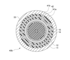
- Comparative cable 40b shown in FIG. 10B is a coaxial cable (double ferrite coaxial cable) with two layers of magnetic resin as a magnetic shield.
- Comparative cable 40b is provided with, from the inside, a signal line 11, an insulating layer 12, a conductor sheet 14, a braided wire 15, an inner magnetic resin layer 41a, an outer shield layer 42, an outer magnetic resin layer 41b, and an outer sheath layer 33.
- the signal line 11, the insulating layer 12, the conductor sheet 14, and the braided wire 15 form the transmission section.
- the two magnetic resin layers 41a and 41b sandwiching the outer shield layer 42 function as a magnetic shield.
- Emission and immunity measurements were performed in an anechoic chamber for three types of cables: comparative cable 40a, comparative cable 40b, and cable 100 described in this embodiment.
- the length of each cable used in the measurements was 1.7 m. Measurements were also performed by switching antennas depending on the measurement frequency. Specifically, a biconical antenna was used for measurements from 30 MHz to 300 MHz, and a log periodic antenna was used for measurements from 300 MHz to 1 GHz.
- each measurement was performed by switching the antenna orientation between horizontal and vertical. By looking at the measurement results when the antenna was placed in both horizontal and vertical directions, it is possible to properly evaluate the strength of the spatial noise radiated from the antenna and the spatial noise entering the antenna.
- FIG. 11A and 11B are schematic diagrams showing an example of emission measurement, in which Fig. 11A shows an example of an arrangement for emission measurement using a biconical antenna 43, and Fig. 11B shows an example of an arrangement for emission measurement using a log periodic antenna 45.
- the measurement cables to be measured were positioned horizontally.
- the biconical antenna 43 and log periodic antenna 45 were positioned so that the minimum distance to the radio wave absorbing material 47 installed on the wall of the anechoic chamber was 1 m, and the distance to the measurement cable was 3 m.
- the distance between the center position 44 and the measurement cable was set to 3 m.
- the distance between the tip 46 on the side where the shortest antenna element is located and the measurement cable was set to 3 m.
- One end of the measurement cable was connected to a signal generator 48 that outputs a measurement signal, and the other end of the measurement cable was terminated at 50 ⁇ , which is the impedance of the coaxial line.
- the biconical antenna 43 and the log periodic antenna 45 were connected to a spectrum analyzer 49 that detects frequency components.
- a 10 dBm signal was output from the signal generator 48 while sweeping the frequency, and this signal was applied to a measurement cable terminated at 50 ⁇ .
- the power level radiated from the measurement cable was measured using a biconical antenna 43 and a log periodic antenna 45.
- the power level radiated from the measurement cable may be referred to as the radiation intensity of the measurement cable.
- Figures 12 and 13 are graphs showing the results of emission measurements.
- Figure 12 shows the results of emission measurements from 30 MHz to 300 MHz measured using a biconical antenna 43
- Figure 13 shows the results of emission measurements from 300 MHz to 1 GHz measured using a log periodic antenna 45.
- the horizontal axis of each graph is frequency, and the vertical axis is power level, which indicates the radiation intensity of the measured cable.
- the measurement result of comparative cable 40a is marked “#1"
- the measurement result of comparative cable 40b is marked “#2”
- the measurement result of cable 100 is marked “#3”.
- the measurement when the antenna direction is horizontal is marked “Horizontal”
- the measurement when the antenna direction is vertical is marked “Vertical”.
- the results of emission measurements from 30 MHz to 300 MHz will be described.
- the radiation intensity of the comparative cable 40a is generally -70 dBm or more over the entire measurement range, including peaks exceeding -50 dBm.
- the radiation intensity of the comparative cable 40a is generally -80 dBm or less over the entire measurement range, which is smaller than when the antenna direction is horizontal.
- the radiation intensity of the comparative cable 40b is ⁇ 70 dBm or less over the entire measurement range when the antenna direction is horizontal, whereas the radiation intensity of the comparative cable 40a may be ⁇ 70 dBm or more when the antenna direction is vertical.
- the radiation intensity of cable 100 to which this technology is applied is approximately -80 dBm or less on the low frequency side of the measurement range, and even at high radiation intensity, is -70 dBm or less throughout the entire measurement range.
- the radiation intensity of cable 100 is at most -80 dBm. In other words, in the range of 30 MHz to 300 MHz, it can be said that the radiation intensity of cable 100 to which this technology is applied is sufficiently suppressed compared to comparative cable 40a and comparative cable 40b.
- the results of the emission measurement from 300 MHz to 1 GHz will be described with reference to FIG. 13, when the antenna direction is horizontal, the radiation intensity of the comparative cable 40a includes multiple peaks exceeding -70 dBm over the entire measurement range, and peaks exceeding -60 dBm are also measured on the low frequency side.
- the radiation intensity of the comparative cable 40a is smaller than when the antenna direction is horizontal, and is -80 dBm or less except for the low frequency side of the measurement range. As shown in the middle of Fig.
- the radiation intensity of the comparative cable 40b when the antenna direction is horizontal, includes peaks exceeding -70 dBm on the high frequency side, but is below -70 dBm on the low frequency side, and does not have peaks exceeding -60 dBm as seen in the comparative cable 40a. Note that when the antenna direction is vertical, the same as when it is horizontal, and the radiation intensity is greater than that of the comparative cable 40a.
- the radiation intensity of cable 100 to which this technology is applied is smaller than that of comparison cable 40b on the low frequency side of the measurement range, and is about the same as that of comparison cable 40b on the high frequency side.
- the antenna direction is vertical, the radiation intensity of cable 100 is about the same as that of comparison cable 40a, but smaller than that of comparison cable 40b. In other words, even in the range of 300 MHz to 1 GHz, it can be said that the radiation intensity of cable 100 to which this technology is applied is sufficiently suppressed compared to comparison cable 40a and comparison cable 40b.
- FIG. 14A and 14B are schematic diagrams showing an example of immunity measurement, in which Fig. 14A shows an example of the arrangement for immunity measurement using a biconical antenna 43, and Fig. 14B shows an example of the arrangement for immunity measurement using a log periodic antenna 45.
- the arrangement of the measurement cables (comparison cable 40a, comparison cable 40b, and cable 100) and antennas (biconical antenna 43 and log periodic antenna 45) in the immunity measurement is the same as that in the emission measurement.
- One end of the measurement cable was connected to a spectrum analyzer, and the other end of the measurement cable was terminated at 50 ⁇ .
- the biconical antenna 43 and the log periodic antenna 45 were connected to a signal generator 48.
- the immunity measurement a 10 dBm signal was output from the signal generator 48 while sweeping the frequency, and this signal was applied to the biconical antenna 43 and the log periodic antenna 45. At this time, the power level of the measurement cable was measured using the spectrum analyzer 49. Below, the power level of the measurement cable may be referred to as the reception strength of the measurement cable.
- Figures 15 and 16 are graphs showing the results of immunity measurements.
- Figure 15 shows the results of an immunity measurement when a signal from 30 MHz to 300 MHz was input to the biconical antenna 43
- Figure 16 shows the results of an immunity measurement when a signal from 300 MHz to 1 GHz was input to the log periodic antenna 45.
- the horizontal axis of each graph is frequency
- the vertical axis is power level, which indicates the reception strength of the measurement cable.
- the reception strength of the comparative cable 40a is generally greater than or equal to -80 dBm over the entire measurement range, and peaks exceeding -60 dBm are also measured.
- the reception strength of the comparative cable 40a includes peaks exceeding -70 dBm and peaks exceeding -80 dBm.
- the reception strength of the comparative cable 40b includes multiple peaks exceeding -80 dBm, but is generally lower than that of the comparative cable 40a.
- the reception strength of the comparative cable 40b is approximately -90 dBm.
- the reception strength of cable 100 to which this technology is applied is approximately -90 dBm on the low frequency side of the measurement range when the antenna direction is horizontal, and at most -80 dBm on the high frequency side. Furthermore, the reception strength of cable 100 is approximately -90 dBm throughout the entire measurement range when the antenna direction is vertical. In other words, in the range of 30 MHz to 300 MHz, it can be said that the reception strength of cable 100 to which this technology is applied is sufficiently suppressed compared to comparison cable 40a and comparison cable 40b.
- the reception strength of the comparison cable 40a includes multiple peaks exceeding -80 dBm over the entire measurement range, and peaks exceeding -70 dBm are also measured on the low frequency side.
- the reception strength of the comparison cable 40a has multiple peaks of about -80 dBm.
- the reception strength of the comparative cable 40b includes multiple peaks exceeding -80 dBm, similar to the comparative cable 40a, but there is no peak exceeding -70 dBm seen on the low frequency side of the comparative cable 40a.
- the reception strength of the comparative cable 40b is approximately -80 dBm over the entire measurement range, which is greater than the reception strength of the comparative cable 40a.
- the reception strength of cable 100 to which this technology is applied is approximately -80 dBm or less on the low frequency side of the measurement range, and is similar to that of comparison cables 40a and 40b on the high frequency side.
- the reception strength of cable 100 is -80 dBm or less throughout the entire measurement range, and there are no peaks included in comparison cables 40a and 40b. In other words, even in the range of 300 MHz to 1 GHz, it can be said that the reception strength of cable 100 to which this technology is applied is sufficiently suppressed compared to comparison cables 40a and 40b.
- the radiation intensity and reception intensity of cable 100 are much smaller than those of comparison cable 40a, which is a normal coaxial cable.
- the radiation intensity and reception intensity of cable 100 are also sufficiently reduced compared to comparison cable 40b, which is wrapped with two layers of magnetic resin. In other words, it has become clear that cable 100 to which this technology is applied exhibits extremely high noise resistance performance in emission and immunity measurements.
- the magnetic tape 20 wrapped around the transmission section 10 is covered with the magnetic resin layer 30.
- shielding performance is maintained even if gaps or the like occur in the magnetic tape 20 due to bending. As a result, it is possible to realize a cable that suppresses noise intrusion and radiation and whose performance is less likely to deteriorate even when bent.
- the magnetic shield of a cable is made of magnetic resin
- magnetic materials such as ferrite are dispersed in the synthetic resin that is the base material of the magnetic resin.
- the magnetic flux is cut by the synthetic resin within the magnetic resin, making it difficult to increase the magnetic permeability, and the effect as a magnetic shield cannot be fully improved.
- the magnetic resin can completely seal and cover the transmission section that forms the core of the cable, there is no significant degradation in performance.
- magnetic shield of a cable using only magnetic tape.
- magnetic tapes that achieve high magnetic permeability have been developed by forming a magnetic layer on the surface of tape material containing metals such as aluminum through coating or deposition to align the orientation. Such magnetic tapes are used in USB cables and the like.
- magnetic tape has high magnetic permeability, any gaps that may occur may allow noise to enter or radiate, reducing its effectiveness as a magnetic shield.
- the magnetic tape 20 is covered with a magnetic resin layer 30. That is, the cable 100 is configured such that a tape coated with a magnetic material is covered with a resin in which the magnetic material is dispersed. In this way, by winding the magnetic tape 20 and then covering it with the magnetic resin layer 30, noise does not leak from the gaps in the magnetic tape 20. In addition, because the magnetic flux is coupled in the gaps in the magnetic tape 20 by the magnetic resin layer 30, it is possible to realize a magnetic shield by the entire cable 100 due to the high magnetic permeability of the magnetic tape 20.
- the magnetic permeability is high, the high frequency impedance is high, making it possible to significantly reduce the conducted noise received from the device to which the cable 100 is connected.
- the spatial noise radiated noise
- the cable 100 is bent, and a magnetic shield were to be formed using only the magnetic tape 20, the gaps in the magnetic tape 20 would become larger, which could result in a deterioration in shielding performance.
- the cable 100 has a magnetic resin layer 30 around the magnetic tape 20, so that even if the gaps in the magnetic tape 20 become larger due to bending, the magnetic flux is less likely to be cut off, and the shielding performance is less likely to deteriorate. For this reason, it is possible to sufficiently suppress the high-frequency current that enters the cable 100, even when the cable 100 is bent.
- the magnetic material in the magnetic tape 20 it is possible to achieve high magnetic permeability without increasing the thickness of the magnetic layer 24.
- the diameter of the cable 100 it is possible to make the diameter of the cable 100 sufficiently small compared to, for example, the comparative cable 40b described above, which has two layers of magnetic resin.
- the thin magnetic tape 20 it is possible to achieve a diameter that is almost the same as that of a conventional cable that does not have a magnetic shield, such as the comparative cable 40a.
- the magnetic tape 20 can be wound horizontally, and can be configured without impairing the flexibility of the cable 100. This makes it possible to realize a cable 100 that is highly flexible and easy to handle, without performance degradation due to bending.
- the magnetic layer 24 is provided on both sides (the inner surface and the outer surface) of the tape substrate 21 in the magnetic tape 20.
- this is not limited thereto, and the magnetic layer 24 may be formed on one side of the tape substrate 21.
- 17 is a schematic diagram showing another example of the configuration of a magnetic tape 20a, in which a magnetic layer 24 is formed on one side of a tape substrate 21.
- the magnetic tape 20a has, in order from the inside, an adhesive layer 25, a resin substrate 22, a metal layer 23, and a magnetic layer 24.
- the resin substrate 22 and the metal layer 23 form the tape substrate 21. That is, in the magnetic tape 20a, the adhesive layer 25 is formed on the inside of the tape substrate 21 (the inside of the resin substrate 22), and the magnetic layer 24 is formed on the outside of the tape substrate 21 (the outside of the metal layer 23).
- the magnetic tape 20a has a configuration similar to that of the magnetic tape 20 described with reference to FIG. 3A etc., except that the inner magnetic layer 24a has been eliminated and only the outer magnetic layer 24b remains.
- the magnetic tape 20a is wound around the transmission section 10 (see FIG. 3A, etc.) with the magnetic layer 24 on the outside.
- the magnetic tape 20a is typically wound horizontally.
- the magnetic tape 20a wound around the transmission section 10 is covered with a magnetic resin layer 30. In this way, by forming the magnetic layer 24 on the surface facing outward of the tape substrate 21, the magnetic flux is not interrupted in the gaps in the magnetic tape 20, making it possible to significantly improve performance as a magnetic shield.
- the magnetic layer 24 is formed only on the inside of the tape substrate 21. Even in this case, the magnetic layer 24 has high magnetic permeability, making it possible to sufficiently suppress, for example, conductive noise transmitted through a cable.
- the magnetic resin layer 30 formed on the outside of the magnetic layer 24 also functions as a magnetic shield, making it possible to sufficiently attenuate, for example, spatial noise entering from outside the cable.
- a tape-shaped member in which the metal layer 23 is formed on the resin base material 22 has been described as the tape base material 21.
- the present invention is not limited to this, and a metal tape base material 21 that does not include the resin base material 22 may be used.
- Fig. 18 is a schematic diagram showing another example of the configuration of a magnetic tape.
- a tape substrate 21 is a metal tape made of a metal foil made of any one of aluminum, copper, and iron.
- the magnetic tape 20b has, in order from the inside, an adhesive layer 25, an inner magnetic layer 24a, a metal layer 23, and an outer magnetic layer 24b.
- the metal layer 23 is a metallic tape made of metal foil, and is the tape substrate 21 of the magnetic tape 20b. That is, in the magnetic tape 20b, the magnetic layers 24 (the inner magnetic layer 24a and the outer magnetic layer 24b) are formed on both sides of the metallic tape substrate 21 (metal layer 23) which is made without using a resin substrate or the like. In this way, the magnetic tape 20b can be said to have a configuration in which the resin substrate 22 has been eliminated from the magnetic tape 20 described with reference to FIG. 3A etc.
- the metallic tape substrate 21 itself functions as an electric field shield, making it possible to reflect, for example, the electric field components of spatial noise that enter the cable from outside. This makes it possible to make the magnetic tape 20b thinner overall while maintaining shielding performance, compared to the magnetic tape 20 shown in FIG. 3A, for example.
- the adhesive layer is provided on the innermost side of the magnetic tape.
- the adhesive layer may be provided on the outermost side of the magnetic tape.
- the magnetic tape may also be used with the inner and outer sides reversed. In other words, the magnetic tape may be used so that the adhesive layer is located on the outermost side.
- the magnetic tape is wound horizontally so that it partially overlaps. At that time, the inner and outer magnetic tapes are adhered to each other at the overlapping parts. Even with this configuration, it is possible to achieve high shielding performance by providing a magnetic resin layer on the outer side of the magnetic tape.
- the tape substrate of the magnetic tape does not need to have a metal layer.
- a resin substrate alone may be used as the tape substrate, and an oriented magnetic layer may be formed on both sides (or one side) of the resin substrate.
- the magnetic tape will no longer function as an electric field shield, but it is possible to configure an effective magnetic shield using the magnetic layer with high magnetic permeability. It is also possible to eliminate the adhesive layer of the magnetic tape.
- the method of winding the magnetic tape is not limited to this.
- the magnetic tape may also be wound in other ways.
- the magnetic tape may be wound transversely around the transmission section so that the side end faces of the magnetic tape are in contact with each other. That is, the magnetic tape may be wound in a spiral shape so that the magnetic tape does not overlap in the width direction and so that no gaps are formed between the side end faces of the magnetic tape.
- the magnetic tape may be wound transversely around the transmission section so that there is a gap between the side end faces. In this case, the amount of magnetic tape used is reduced, making it possible to reduce the material cost of the cable.
- the gap between the side end faces is filled with a magnetic resin layer, making it possible to make it difficult for the magnetic flux to be cut off.
- the magnetic tape may be wound vertically.
- the magnetic tape When the magnetic tape is wound vertically, the magnetic tape is wound tightly around the surface of the transmission section so that the extension direction of the magnetic tape coincides with the extension direction of the transmission section.
- the magnetic tape may be wound lengthwise around the transmission section so that the side end faces overlap in the width direction, thereby making it possible to completely cover the transmission section with the magnetic tape.
- the magnetic tape may be wound vertically so that its side end faces are in contact and so as to cover the transmission section. That is, the magnetic tape may be wound to encase the transmission section so that it does not overlap in the width direction and so that no gaps are formed between the side end faces of the magnetic tape.
- the magnetic tape may be wound vertically around the transmission section so that there is a gap between the side end faces. Even in this case, the gap between the side end faces is filled with a magnetic resin layer, making it possible to make it difficult for the magnetic flux to be cut off.
- the present invention is not limited to this, and an intermediate layer may be formed between the magnetic tape and the magnetic resin layer.
- the intermediate layer is, for example, a resin layer for improving the adhesion of the magnetic resin layer to the magnetic tape. In this case, for example, when the cable is bent, a gap is unlikely to occur between the magnetic tape and the magnetic resin layer, making it possible to suppress the deterioration of the shielding performance due to bending.
- the type of the intermediate layer is not limited.
- the thickness of the intermediate layer is set to a value that allows the magnetic resin layer to function as a magnetic flux connection layer in the gaps between the magnetic tapes. This can improve the shielding performance of the cable.
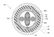
- Figure 19 is a cross-sectional view of a USB 2.0 cable.
- the cable 101 shown in Figure 19 has five wires: a pair of signal cables 50a (D-) and 50b (D+) for differential transmission, power cables 51a and 51b, and a drain wire 52 as a ground wire.
- the signal cables 50a and 50b and the power cables 51a and 51b each have an insulating coating covering the periphery of their core wires.
- Copper is used for the core wire, and either a single wire or a stranded wire consisting of thin wires twisted together to form a single wire may be used.
- the signal cables 50a and 50b are twisted pair cables.
- the signal cables 50a, 50b and the power cables 51a, 51b are covered from the inside out with an aluminum foil shield 53 and a copper wire mesh shield 54.
- the drain wire 52 and the aluminum foil shield 53 are electrically connected.
- a magnetic tape 57 is wound around the copper wire mesh shield 54, and a magnetic resin layer 58 that covers the magnetic tape 57 is formed around the magnetic tape 57.
- an outer sheath layer 59 which is the outermost layer, is provided around the magnetic resin layer 58.
- a USB 2.0 cable 101 to which this technology is applied can suppress noise and also suppress performance degradation due to bending.
- FIG 20 is a cross-sectional view of a USB 3.0 cable.
- the cable 102 shown in Figure 20 has four wires, namely, a pair of signal cables 60a and 60b for differential transmission and power cables 61a and 61b, similar to the USB 2.0 cable 101.
- the signal cables 60a and 60b are called UTP (Unshielded Twisted Pair).
- the cable 102 has USB 3.0 signal cables 62a and 62b and a drain wire 62c, and other USB 3.0 signal lines 63a and 63b and a drain wire 63c.
- the signal cables 62a and 62b are called SDP (Shielded Differential Pair).
- a filler 64 is used as an option. These wires and the filler are covered by a copper wire mesh shield 65.
- a magnetic tape 67 is wound around the copper wire mesh shield 65, and a magnetic resin layer 68 that covers the magnetic tape 67 is formed around the magnetic tape 67.
- an outer sheath layer 69 which is the outermost layer, is provided around the magnetic resin layer 68.
- a USB 3.0 cable 102 to which this technology is applied can suppress noise and also suppress performance degradation due to bending.
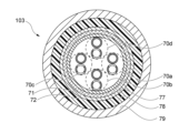
- FIG 21 is a cross-sectional view of an Ethernet cable (LAN cable).
- LAN cable 103 shown in Figure 21, four pairs of signal lines 70a, 70b, 70c, and 70d in a twisted pair cable configuration are covered with a shield.
- the shield is made by layering a conductor sheet 71 made of a PET base material with thin aluminum and a braided wire 72 from the inside.
- a magnetic tape 77 is wound around the braided wire 72, and a magnetic resin layer 78 that covers the magnetic tape 77 is formed around the magnetic tape 77.
- An outer sheath layer 79 which is the outermost layer, is also provided around the magnetic resin layer 78.
- a LAN cable 103 to which this technology is applied can suppress noise and also suppress performance degradation due to bending.
- the two-core cable 104 shown in FIG. 22 has two transmission lines 80a and 80b.
- the two-core cable 104 is a signal cable, and the transmission lines 80a and 80b are signal transmission lines.
- the two-core cable 104 is a power cable, and the transmission lines 80a and 80b function as a hot line and a ground line.
- the two-core cable 104 has a shielding configuration similar to that of the cable 100 shown in FIG. 3A and FIG. 3B.
- the insulator 81 may be resin or a fiber thread such as cotton thread to make the cross section of the two-core cable 104 circular.
- a magnetic tape 87 is wound around the braided wire 83, and a magnetic resin layer 88 that covers the magnetic tape 87 is formed around the magnetic tape 87.
- An outer jacket layer 89 which is the outermost layer, is also provided around the magnetic resin layer 88.
- a two-core cable 104 to which this technology is applied can suppress noise and also suppress deterioration of performance due to bending.
- the magnetic tape 87 is formed on a shield layer consisting of the conductor sheet 82 and the braided wire 83, but it is also possible to eliminate the shield layer.
- the cable according to the present technology may be configured as any one of a signal cable, a power cable, and an in-vehicle cable.
- a signal cable a power cable
- an in-vehicle cable an in-vehicle cable.
- the above-mentioned coaxial cable 100, the USB 2.0 cable 101, the USB 3.0 cable 102, the LAN cable 103, and the two-core cable 104 are examples of signal cables.
- the above-mentioned two-core cable 104 is also an example of a power cable.
- the magnetic tape is wound around a shielding layer such as the copper wire mesh shield 54, the copper wire mesh shield 65, the braided wire 72, and the braided wire 83, but it is also possible to wind the magnetic tape around each cable directly or around a filler or insulator that has a circular cross section.
- the cable according to this technology is configured as an on-board cable that is mounted in equipment requiring noise resistance, such as an automobile, and connects the various devices and sensors of the automobile.
- the terms “same,” “equal,” “orthogonal,” etc. are concepts that include “substantially the same,” “substantially equal,” “substantially orthogonal,” etc. For example, they also include states that fall within a specified range (e.g., a range of ⁇ 10%) based on “completely the same,” “completely equal,” “completely orthogonal,” etc.
- the present technology can also be configured as follows.
- a transmission section having at least one transmission line for transmitting a signal or power; a magnetic tape having a magnetic layer that absorbs radio waves and wound around the transmission section; A cable comprising: a magnetic resin layer that is made of a magnetic resin that absorbs radio waves and that covers the magnetic tape.
- the magnetic tape has a tape substrate on which the magnetic layer is formed, The magnetic layer is formed on one or both sides of the tape substrate.
- the cable according to (2), The magnetic layer is formed on at least a surface of the tape substrate facing outward.
- the cable according to (2) or (3), The cable, wherein the tape base material is a resin tape formed from a polyester resin or a polyolefin resin.
- the tape base material is a metal tape made of a metal foil made of any one of aluminum, copper, and iron.
- the magnetic layer is a coating layer of a magnetic material applied to the surface of the tape base material so that the magnetic material is oriented.
- the magnetic tape is wound laterally around the transmission portion of the cable.
- the cable according to (9), The magnetic tape is wound laterally around the transmission portion so as to overlap in the width direction of the cable.
- a cable according to any one of (1) to (10), the transmission section includes a shield layer surrounding the at least one transmission line; The magnetic tape is wrapped around the shielding layer of the cable.
- the magnetic layer comprises a magnetic material comprising at least one of iron powder, ferrite powder, or carbon powder.
- the magnetic resin comprises a synthetic resin as a base material and a magnetic material made of at least one of iron powder, ferrite powder, and carbon powder.
- the cable according to (14), The magnetic resin contains iron powder or ferrite powder, A cable in which the proportion of iron powder or ferrite powder contained in the magnetic resin is 70% or more and 90% or less by weight in the magnetic resin.
- a cable according to any one of (1) to (16), A cable configured as one of a coaxial cable, a USB cable, a signal cable, a power cable, and an automotive cable.
- (18) forming a transmission section having at least one transmission line for transmitting a signal or power; a step of wrapping a magnetic tape having a magnetic layer that absorbs radio waves around the transmission section; and a step of covering the magnetic tape with a magnetic resin that absorbs radio waves to form a magnetic resin layer.
- a method for producing the cable according to (18), comprising the steps of:
- the magnetic resin layer is a resin coating formed by extruding the magnetic resin onto an intermediate body in which the magnetic tape is wound around the transmission section.
Landscapes
- Engineering & Computer Science (AREA)
- Chemical & Material Sciences (AREA)
- Dispersion Chemistry (AREA)
- Power Engineering (AREA)
- Physics & Mathematics (AREA)
- Spectroscopy & Molecular Physics (AREA)
- Microelectronics & Electronic Packaging (AREA)
- Insulated Conductors (AREA)
Abstract
Description
前記伝送部は、信号又は電力を伝送する少なくとも1つの伝送線を有する。
前記磁性テープは、電波を吸収する磁性層を有し、前記伝送部の周囲に巻かれる。
前記磁性樹脂層は、電波を吸収する磁性樹脂からなり、前記磁性テープを被覆する。
信号又は電力を伝送する少なくとも1つの伝送線を有する伝送部を形成する工程。
電波を吸収する磁性層を有する磁性テープを前記伝送部の周囲に巻き付ける工程。
電波を吸収する磁性樹脂を前記磁性テープに被覆して磁性樹脂層を形成する工程。
図1は、近傍界及び遠方界について説明するためのグラフである。ここでは、アンテナが発生する電磁界の特性について説明する。例えば、アンテナの近くで電磁シールドを使う場合、シールドの効果は波動インピーダンスにより変化する。ここで、波動インピーダンスとは、ある場所における電界(E)と磁界(H)の比率(E/H)である。
図3Aは、本実施形態に係るケーブルの構成例を示す模式的な断面図である。図3Bは、本実施形態に係るケーブルの構成例を示す模式的な側面図である。図3Aは、ケーブル100の中心を通る中心線に直交する面でケーブル100を切断した断面図であり、図3Bは、中心線に直交する方向から見たケーブル100の側面図である。
ケーブル100は、伝送部10、磁性テープ20、磁性樹脂層30(内部シース)、及び外被層33を有する。
ポリエステル系樹脂は、例えば、PET(ポリエチレンテレフタレート)、PEN(ポリエチレンナフタレート)、PBT(ポリブチレンテレフタレート)、PBN(ポリブチレンナフタレート)、PCT(ポリシクロヘキシレンジメチレンテレフタレート)、PEB(ポリエチレン-p(オキシベンゾエート)、およびポリエチレンビスフェノキシカルボキシレートからなる群より選ばれた少なくとも1種を含む。樹脂基材22が2種以上のポリエステル系樹脂を含む場合、それらの2種以上のポリエステル系樹脂は混合されていてもよいし、共重合されていてもよいし、または積層されていてもよい。ポリエステル系樹脂の末端および側鎖の少なくとも一方が変性されていてもよい。樹脂基材22は、ポリエステル系樹脂に加えて、後述のポリエステル系樹脂以外の樹脂を含んでもよい。
本実施形態では、磁性層24は、テープ基材21の表面に磁性粉26(磁性材料)が配向するように塗布された磁性粉26の塗布層である。
蒸着やスパッタを用いる場合、各磁性粉26はテープ基材21上に積層される過程で配向される。これらの方法により、例えば磁性層24として緻密な積層膜を所望の膜厚で構成することが可能となる。
μ=μ'-jμ'' ・・・(1)
磁性樹脂層30は、磁性テープ20を直接被覆することが好ましい。ここで、磁性テープ20を直接被覆することは、磁性テープ20の外側の表面と磁性樹脂とが接触するように磁性樹脂層30を設けることである。
本実施形態では、磁性テープ20の最も外側に外側磁性層24bが形成される。磁性樹脂層30は、この外側磁性層24bを直接被覆する。すなわち、磁性樹脂層30は、磁性テープ20(外側磁性層24b)の外側の表面に接触した状態で磁性テープ20(外側磁性層24b)の周囲を覆うように構成される。
なお、磁性樹脂層30に含まれる磁性粉26と、上記した磁性テープ20の磁性層24を構成する磁性粉26の種類は、同じであってもよいし、異なっていてもよい。
磁性テープ20を構成する磁性層24は、磁性材料(磁性粉26)の配向を整えて、テープ基材21上に塗布や蒸着等により形成された層である(図5参照)。このため、例えば磁性材料(磁性粉26)が合成樹脂32の中に分散されて構成されている磁性樹脂31(図7参照)と比べて、磁性テープ20の透磁率は非常に高くなる。
特にケーブル100が屈曲した場合には、重複部27における隙間等が拡大し、磁性テープ20によるシールド性能が大きく低下する可能性がある。
図8は、ケーブルの製造方法の一例を示すフローチャートである。図9は、ケーブルを製造する工程について説明するための模式図である。以下では、図8及び図9を参照してケーブル100の製造方法について説明する。
なお導体シート14の巻き方は縦巻きでもよい。縦巻きは、例えばシートの延長方向が、巻き付ける対象となる線材の延長方向と一致するように、線材の表面にシートを密着させて巻き付ける方法である。この場合、導体シート14の延長方向に沿った端部同士が重なるように、絶縁層12の周りに導体シート14が縦巻きされる。
磁性テープ20を製造する工程では、まず表面に金属層23を設けた樹脂基材22(テープ基材21)が形成される。例えば金属層23となるアルミ箔が、樹脂基材22に貼り付けられる。
このように製造された磁性テープ20が、所定のフィーダーから中間線材16aに巻き付けられ、中間線材16bが形成される。
押出成形では、上記したように、磁性テープ20の周囲に溶融した磁性樹脂31が供給される。このため、重複部27において磁性層24の切れ目となる側端面28を含め、磁性テープ20全体が隙間なく磁性樹脂31に覆われる。これにより、磁性テープ20同士の隙間等において磁束が切れて伝送部10にノイズが侵入するといった事態を十分に回避することが可能となる。
以下では、図3A及び図3B等を参照して説明した本実施形態に係るケーブル100についてのノイズ特性の評価について説明する。ノイズ特性の評価としては、ケーブル100から放射される空間ノイズを測定したエミッション測定(放射ノイズ評価)と、ケーブル100に侵入する空間ノイズを測定したイミュニティ測定(耐ノイズ評価)とを行った。また各測定では、比較のために2種類の比較用ケーブルを用いた。
図10Aに示す比較用ケーブル40aは、磁気シールドの設けられていない通常の同軸ケーブルである。比較用ケーブル40aでは、内側から順番に、信号線11と、絶縁層12と、導体シート14と、編組線15と、外被層33とが設けられる。すなわち比較用ケーブル40aでは、伝送部(信号線11、絶縁層12、導体シート14、編組線15)の周りに磁性材料を用いた層(磁気シールドとなる層)は設けられていない。
図11A及び図11Bは、エミッション測定の一例を示す模式図である。図11Aは、バイコニカルアンテナ43を用いたエミッション測定の配置例を示す図であり、図11Bは、ログペリオディックアンテナ45を用いたエミッション測定の配置例を示す図である。
図12の上段に示すように、比較用ケーブル40aの放射強度は、アンテナ方向が水平である場合、測定範囲全体で概ね-70dBm以上となり、-50dBmを超えるピークも含む。なお、比較用ケーブル40aの放射強度は、アンテナ方向が垂直である場合、測定範囲全体で概ね-80dBm以下となり、水平の場合と比べて小さい。
図12の中段に示すように、比較用ケーブル40bの放射強度は、アンテナ方向が水平である場合、測定範囲全体で-70dBm以下となる。一方で、比較用ケーブル40aの放射強度は、アンテナ方向が垂直である場合、-70dBm以上となる場合もある。
図13の上段に示すように、比較用ケーブル40aの放射強度は、アンテナ方向が水平である場合、測定範囲全体に-70dBmを超える複数のピークを含み、低周波数側では-60dBmを超えるピークも測定される。なお、比較用ケーブル40aの放射強度は、アンテナ方向が垂直である場合、水平の場合と比べて小さく、測定範囲の低周波数側を除くと-80dBm以下である。
図13の中段に示すように、比較用ケーブル40bの放射強度は、アンテナ方向が水平である場合、高周波数側では-70dBmを超えるピークを含むが、低周波数側では-70dBm以下であり、比較用ケーブル40aに見られるような-60dBmを超えるピークはない。なお、アンテナ方向が垂直である場合も、水平の場合と同様であり、比較用ケーブル40aと比べると、放射強度が大きい。
図14A及び図14Bは、イミュニティ測定の一例を示す模式図である。図14Aは、バイコニカルアンテナ43を用いたイミュニティ測定の配置例を示す図であり、図14Bは、ログペリオディックアンテナ45を用いたイミュニティ測定の配置例を示す図である。
なお測定ケーブルの一端は、スペクトラムアナライザーに接続し、測定ケーブルの他端は、50Ωで終端した。またバイコニカルアンテナ43及びログペリオディックアンテナ45は、シグナルジェネレータ48に接続した。
図15の上段に示すように、比較用ケーブル40aの受信強度は、アンテナ方向が水平である場合、測定範囲全体で概ね-80dBm以上となり、-60dBmを超えるピークも測定される。また、比較用ケーブル40aの受信強度は、アンテナ方向が垂直である場合、-70dBmを超えるピークや-80dBmを超えるピークを含む。
図15の中段に示すように、比較用ケーブル40bの受信強度は、アンテナ方向が水平である場合、-80dBmを超える複数のピークを含むが、全体として比較用ケーブル40aよりも受信強度が低い。またアンテナ方向が垂直である場合、比較用ケーブル40bの受信強度は、概ね-90dBmとなる。
図16の上段に示すように、アンテナ方向が水平である場合、比較用ケーブル40aの受信強度は、測定範囲全体に-80dBmを超える複数のピークを含み、低周波数側では-70dBmを超えるピークも測定される。なお、比較用ケーブル40aの受信強度は、アンテナ方向が垂直である場合、-80dBm程度の複数のピークをもつ。
図16の中段に示すように、比較用ケーブル40bの受信強度は、アンテナ方向が水平である場合、比較用ケーブル40aと同様に-80dBmを超える複数のピークを含むが、比較用ケーブル40aの低周波数側に見られる-70dBmを超えるようなピークはない。また、比較用ケーブル40bの受信強度は、アンテナ方向が垂直である場合、測定範囲全体で概ね-80dBmとなり、比較用ケーブル40aよりも受信強度が大きい。
本技術は、以上説明した実施形態に限定されず、他の種々の実施形態を実現することができる。
図17は、磁性テープの他の構成例を示す模式図である。図17に示す磁性テープ20aでは、テープ基材21の片面に磁性層24が形成される。
図18は、磁性テープの他の構成例を示す模式図である。図18に示す磁性テープ20bでは、テープ基材21は、アルミ、銅、又は鉄のいずれかの金属からなる金属箔で構成された金属製のテープである。
磁性テープは、他の方法で横巻されてもよい。
例えば、磁性テープは、その側端面が接するように伝送部に横巻きされてもよい。すなわち、磁性テープが幅方向で重ならず、かつ、磁性テープの側端面の間に隙間ができないように螺旋状に巻かれてもよい。この場合、例えば磁性テープの側端面の間に、屈曲により隙間ができることも考えられるが、磁性樹脂層により磁性テープを被覆することで、側端面の間で磁束が切れにくくなり、シールド性能の劣化を抑制することが可能である。
また例えば、磁性テープは、側端面の間に隙間ができるように伝送部に横巻されてもよい。この場合、磁性テープの使用量が少なくなりケーブルの材料コストを下げることが可能である。なお、側端面の間の隙間は磁性樹脂層で充填されるため、磁束を切れにくくすることが可能である。
例えば、磁性テープは、その側端面が幅方向に重なるように伝送部に縦巻きされてもよい。これにより、伝送部を磁性テープで完全に覆うことが可能である。
また例えば、磁性テープは、その側端面が接するように、かつ、伝送部を覆うように縦巻きされてもよい。すなわち、磁性テープが幅方向で重ならず、かつ、磁性テープの側端面の間に隙間ができないように、伝送部を包むように巻かれてもよい。この場合でも、磁性樹脂層により磁性テープを被覆することで、ケーブルの屈曲により側端面の間にできる隙間等において磁束が切れにくくなり、シールド性能の劣化を抑制可能である。
また例えば、磁性テープは、側端面の間に隙間ができるように伝送部に縦巻されてもよい。この場合でも、側端面の間の隙間は磁性樹脂層で充填されるため、磁束を切れにくくすることが可能である。
この他、中間層の種類は限定されない。また、中間層の厚みは、例えば磁性樹脂層が磁性テープの隙間において磁束をつなげる機能を発揮できるような厚みに設定される。これにより、ケーブルのシールド性能を向上することが可能である。
また、上記の実施例においては、磁性テープは、銅線網シールド54、銅線網シールド65や編組線72、編組線83のようなシールド層に巻かれているが、それぞれのケーブルに、直接または、充填材や絶縁体で、断面を円形にしたものに磁性テープを巻くことも可能である。
(1)信号又は電力を伝送する少なくとも1つの伝送線を有する伝送部と、
電波を吸収する磁性層を有し、前記伝送部の周囲に巻かれた磁性テープと、
電波を吸収する磁性樹脂からなり、前記磁性テープを被覆する磁性樹脂層と
を具備するケーブル。
(2)(1)に記載のケーブルであって、
前記磁性テープは、前記磁性層が形成されるテープ基材を有し、
前記磁性層は、前記テープ基材の片面又は両面に形成される
ケーブル。
(3)(2)に記載のケーブルであって、
前記磁性層は、少なくとも前記テープ基材の外側に向けられる面に形成される
ケーブル。
(4)(2)又は(3)に記載のケーブルであって、
前記テープ基材は、ポリエステル系樹脂又はポリオレフィン系樹脂によって形成される樹脂製のテープである
ケーブル。
(5)(2)から(4)のうちいずれか1つに記載のケーブルであって、
前記テープ基材は、アルミ、銅、又は鉄のいずれかの金属からなる金属層が形成された樹脂製のテープである
ケーブル。
(6)(2)から(5)のうちいずれか1つに記載のケーブルであって、
前記テープ基材は、アルミ、銅、又は鉄のいずれかの金属からなる金属箔で構成された金属製のテープである
ケーブル。
(7)(2)から(6)のうちいずれか1つに記載のケーブルであって、
前記磁性層は、前記テープ基材の表面に磁性材料が配向するように塗布された前記磁性材料の塗布層である
ケーブル。
(8)(2)から(7)のうちいずれか1つに記載のケーブルであって、
前記磁性層は、前記テープ基材の表面に形成された磁性材料の蒸着膜、又は磁性材料のスパッタ膜である
ケーブル。
(9)(1)から(8)のうちいずれか1つに記載のケーブルであって、
前記磁性テープは、前記伝送部の周囲に横巻きされる
ケーブル。
(10)(9)に記載のケーブルであって、
前記磁性テープは、幅方向に重なるように前記伝送部の周囲に横巻きされる
ケーブル。
(11)(1)から(10)のうちいずれか1つに記載のケーブルであって、
前記伝送部は、前記少なくとも1つの伝送線を囲むシールド層を有し、
前記磁性テープは、前記シールド層の周囲に巻かれる
ケーブル。
(12)(1)から(11)のうちいずれか1つに記載のケーブルであって、
前記磁性テープは、前記伝送部に向けられる面に形成された接着層を有する
ケーブル。
(13)(1)から(12)のうちいずれか1つに記載のケーブルであって、
前記磁性層は、鉄粉、フェライト粉末、又は炭素粉末の少なくとも1つからなる磁性材料を含む
ケーブル。
(14)(1)から(13)のうちいずれか1つに記載のケーブルであって、
前記磁性樹脂は、母材となる合成樹脂と、鉄粉、フェライト粉末、又は炭素粉末の少なくとも1つからなる磁性材料とを含む
ケーブル。
(15)(14)に記載のケーブルであって、
前記磁性樹脂は、鉄粉又はフェライト粉末を含み、
前記磁性樹脂に含まれる鉄粉又はフェライト粉末の割合は、前記磁性樹脂における重量比で70%以上90%以下である
ケーブル。
(16)(1)から(15)のうちいずれか1つに記載のケーブルであって、さらに、
前記磁性樹脂層の周囲を被覆する絶縁性の外被層を具備する
ケーブル。
(17)(1)から(16)のうちいずれか1つに記載のケーブルであって、
同軸ケーブル、USBケーブル、信号ケーブル、電力ケーブル、車載ケーブルのいずれか1つとして構成される
ケーブル。
(18)信号又は電力を伝送する少なくとも1つの伝送線を有する伝送部を形成する工程と、
電波を吸収する磁性層を有する磁性テープを前記伝送部の周囲に巻き付ける工程と、
電波を吸収する磁性樹脂を前記磁性テープに被覆して磁性樹脂層を形成する工程と
を具備するケーブルの製造方法。
(19)(18)に記載のケーブルの製造方法であって、
前記磁性樹脂層は、前記伝送部に前記磁性テープが巻かれた中間体に前記磁性樹脂が押出成形された樹脂被覆である
ケーブルの製造方法。
20、20a、20b、57、67、77、87…磁性テープ
21…テープ基材
22…樹脂基材
23…金属層
24…磁性層
24a…内側磁性層
24b…外側磁性層
25…接着層
30、58、68、78、88…磁性樹脂層
33、59、69、79、89…外被層
100、101、102…ケーブル
103…LANケーブル
104…2芯ケーブル
Claims (19)
- 信号又は電力を伝送する少なくとも1つの伝送線を有する伝送部と、
電波を吸収する磁性層を有し、前記伝送部の周囲に巻かれた磁性テープと、
電波を吸収する磁性樹脂からなり、前記磁性テープを被覆する磁性樹脂層と
を具備するケーブル。 - 請求項1に記載のケーブルであって、
前記磁性テープは、前記磁性層が形成されるテープ基材を有し、
前記磁性層は、前記テープ基材の片面又は両面に形成される
ケーブル。 - 請求項2に記載のケーブルであって、
前記磁性層は、少なくとも前記テープ基材の外側に向けられる面に形成される
ケーブル。 - 請求項2に記載のケーブルであって、
前記テープ基材は、ポリエステル系樹脂又はポリオレフィン系樹脂によって形成される樹脂製のテープである
ケーブル。 - 請求項2に記載のケーブルであって、
前記テープ基材は、アルミ、銅、又は鉄のいずれかの金属からなる金属層が形成された樹脂製のテープである
ケーブル。 - 請求項2に記載のケーブルであって、
前記テープ基材は、アルミ、銅、又は鉄のいずれかの金属からなる金属箔で構成された金属製のテープである
ケーブル。 - 請求項2に記載のケーブルであって、
前記磁性層は、前記テープ基材の表面に磁性材料が配向するように塗布された前記磁性材料の塗布層である
ケーブル。 - 請求項2に記載のケーブルであって、
前記磁性層は、前記テープ基材の表面に形成された磁性材料の蒸着膜、又は磁性材料のスパッタ膜である
ケーブル。 - 請求項1に記載のケーブルであって、
前記磁性テープは、前記伝送部の周囲に横巻きされる
ケーブル。 - 請求項9に記載のケーブルであって、
前記磁性テープは、幅方向に重なるように前記伝送部の周囲に横巻きされる
ケーブル。 - 請求項1に記載のケーブルであって、
前記伝送部は、前記少なくとも1つの伝送線を囲むシールド層を有し、
前記磁性テープは、前記シールド層の周囲に巻かれる
ケーブル。 - 請求項1に記載のケーブルであって、
前記磁性テープは、前記伝送部に向けられる面に形成された接着層を有する
ケーブル。 - 請求項1に記載のケーブルであって、
前記磁性層は、鉄粉、フェライト粉末、又は炭素粉末の少なくとも1つからなる磁性材料を含む
ケーブル。 - 請求項1に記載のケーブルであって、
前記磁性樹脂は、母材となる合成樹脂と、鉄粉、フェライト粉末、又は炭素粉末の少なくとも1つからなる磁性材料とを含む
ケーブル。 - 請求項14に記載のケーブルであって、
前記磁性樹脂は、鉄粉又はフェライト粉末を含み、
前記磁性樹脂に含まれる鉄粉又はフェライト粉末の割合は、前記磁性樹脂における重量比で70%以上90%以下である
ケーブル。 - 請求項1に記載のケーブルであって、さらに、
前記磁性樹脂層の周囲を被覆する絶縁性の外被層を具備する
ケーブル。 - 請求項1に記載のケーブルであって、
同軸ケーブル、USBケーブル、信号ケーブル、電力ケーブル、車載ケーブルのいずれか1つとして構成される
ケーブル。 - 信号又は電力を伝送する少なくとも1つの伝送線を有する伝送部を形成する工程と、
電波を吸収する磁性層を有する磁性テープを前記伝送部の周囲に巻き付ける工程と、
電波を吸収する磁性樹脂を前記磁性テープに被覆して磁性樹脂層を形成する工程と
を具備するケーブルの製造方法。 - 請求項18に記載のケーブルの製造方法であって、
前記磁性樹脂層は、前記伝送部に前記磁性テープが巻かれた中間体に前記磁性樹脂が押出成形された樹脂被覆である
ケーブルの製造方法。
Priority Applications (1)
| Application Number | Priority Date | Filing Date | Title |
|---|---|---|---|
| JP2025502211A JPWO2024176754A1 (ja) | 2023-02-20 | 2024-01-31 |
Applications Claiming Priority (2)
| Application Number | Priority Date | Filing Date | Title |
|---|---|---|---|
| JP2023-024251 | 2023-02-20 | ||
| JP2023024251 | 2023-02-20 |
Publications (1)
| Publication Number | Publication Date |
|---|---|
| WO2024176754A1 true WO2024176754A1 (ja) | 2024-08-29 |
Family
ID=92500981
Family Applications (1)
| Application Number | Title | Priority Date | Filing Date |
|---|---|---|---|
| PCT/JP2024/002978 Ceased WO2024176754A1 (ja) | 2023-02-20 | 2024-01-31 | ケーブル及びケーブルの製造方法 |
Country Status (2)
| Country | Link |
|---|---|
| JP (1) | JPWO2024176754A1 (ja) |
| WO (1) | WO2024176754A1 (ja) |
Citations (5)
| Publication number | Priority date | Publication date | Assignee | Title |
|---|---|---|---|---|
| JP2011249022A (ja) * | 2010-05-24 | 2011-12-08 | Sumitomo Electric Ind Ltd | 光電気複合ケーブル |
| JP2015153734A (ja) * | 2014-02-19 | 2015-08-24 | 日立金属株式会社 | ノイズ抑制ケーブル |
| JP2016225155A (ja) * | 2015-05-29 | 2016-12-28 | 日立金属株式会社 | ケーブル製造装置 |
| WO2019021716A1 (ja) * | 2017-07-25 | 2019-01-31 | 株式会社村田製作所 | 同軸ケーブルおよびその製造方法並びに同軸ケーブル付き同軸コネクタ |
| JP2021068815A (ja) * | 2019-10-24 | 2021-04-30 | 国立大学法人信州大学 | コイルおよびコイルユニットおよび無線電力伝送装置およびコイルの製造方法 |
-
2024
- 2024-01-31 WO PCT/JP2024/002978 patent/WO2024176754A1/ja not_active Ceased
- 2024-01-31 JP JP2025502211A patent/JPWO2024176754A1/ja active Pending
Patent Citations (5)
| Publication number | Priority date | Publication date | Assignee | Title |
|---|---|---|---|---|
| JP2011249022A (ja) * | 2010-05-24 | 2011-12-08 | Sumitomo Electric Ind Ltd | 光電気複合ケーブル |
| JP2015153734A (ja) * | 2014-02-19 | 2015-08-24 | 日立金属株式会社 | ノイズ抑制ケーブル |
| JP2016225155A (ja) * | 2015-05-29 | 2016-12-28 | 日立金属株式会社 | ケーブル製造装置 |
| WO2019021716A1 (ja) * | 2017-07-25 | 2019-01-31 | 株式会社村田製作所 | 同軸ケーブルおよびその製造方法並びに同軸ケーブル付き同軸コネクタ |
| JP2021068815A (ja) * | 2019-10-24 | 2021-04-30 | 国立大学法人信州大学 | コイルおよびコイルユニットおよび無線電力伝送装置およびコイルの製造方法 |
Also Published As
| Publication number | Publication date |
|---|---|
| JPWO2024176754A1 (ja) | 2024-08-29 |
Similar Documents
| Publication | Publication Date | Title |
|---|---|---|
| CA1216641A (en) | Shielded cable | |
| US6416830B2 (en) | Composite magnetic tube and method of producing the same, and electromagnetic interference suppressing tube | |
| US5262591A (en) | Inherently-shielded cable construction with a braided reinforcing and grounding layer | |
| US9087630B2 (en) | Cable barrier layer with shielding segments | |
| CN109215858B (zh) | 电磁波吸收电缆 | |
| WO2004003942A1 (ja) | コネクタ付き信号伝送ケーブル | |
| US20020036096A1 (en) | Electric installation cable | |
| US20230018074A1 (en) | Electric cable | |
| US9706692B2 (en) | Noise shield cable and method of manufacturing the same | |
| JP4032898B2 (ja) | 電気ブレーキ用ノイズ対策ケーブル | |
| US20180268965A1 (en) | Data cable for high speed data transmissions and method of manufacturing the data cable | |
| US12087474B2 (en) | Cable and antenna device with coaxial cable | |
| JP5579215B2 (ja) | ワイヤーハーネスおよびワイヤーハーネスのシールド構造 | |
| CN203812644U (zh) | 基站天线线缆 | |
| JP2004214137A (ja) | 同軸ケーブル | |
| JP2013008793A (ja) | シールドテープ、及び、それを用いたケーブル | |
| CN112712919B (zh) | 屏蔽线束和屏蔽线束的制备方法 | |
| JP2004214138A (ja) | 同軸ケーブル | |
| CN209895793U (zh) | 一种z型屏蔽带及具有z型屏蔽层的电缆 | |
| JP7651977B2 (ja) | 通信用電線 | |
| CN222233350U (zh) | 非接地型对称式铠装通信电缆 | |
| JP3412123B2 (ja) | ケーブル | |
| CN106409424A (zh) | 一种碳纤维金属复合屏蔽线 | |
| CN106782802A (zh) | 一种金属碳纤维复合屏蔽线 | |
| CN205881514U (zh) | 一种抗拉轻质阻燃型屏蔽电缆 |
Legal Events
| Date | Code | Title | Description |
|---|---|---|---|
| 121 | Ep: the epo has been informed by wipo that ep was designated in this application |
Ref document number: 24760061 Country of ref document: EP Kind code of ref document: A1 |
|
| ENP | Entry into the national phase |
Ref document number: 2025502211 Country of ref document: JP Kind code of ref document: A |
|
| WWE | Wipo information: entry into national phase |
Ref document number: 2025502211 Country of ref document: JP |
|
| NENP | Non-entry into the national phase |
Ref country code: DE |
|
| 122 | Ep: pct application non-entry in european phase |
Ref document number: 24760061 Country of ref document: EP Kind code of ref document: A1 |