WO2024176740A1 - 半導体装置および車両 - Google Patents
半導体装置および車両 Download PDFInfo
- Publication number
- WO2024176740A1 WO2024176740A1 PCT/JP2024/002597 JP2024002597W WO2024176740A1 WO 2024176740 A1 WO2024176740 A1 WO 2024176740A1 JP 2024002597 W JP2024002597 W JP 2024002597W WO 2024176740 A1 WO2024176740 A1 WO 2024176740A1
- Authority
- WO
- WIPO (PCT)
- Prior art keywords
- layer
- semiconductor device
- terminal
- conductive layer
- electrode
- Prior art date
- Legal status (The legal status is an assumption and is not a legal conclusion. Google has not performed a legal analysis and makes no representation as to the accuracy of the status listed.)
- Ceased
Links
Images


Classifications
-
- H—ELECTRICITY
- H10—SEMICONDUCTOR DEVICES; ELECTRIC SOLID-STATE DEVICES NOT OTHERWISE PROVIDED FOR
- H10D—INORGANIC ELECTRIC SEMICONDUCTOR DEVICES
- H10D80/00—Assemblies of multiple devices comprising at least one device covered by this subclass
- H10D80/20—Assemblies of multiple devices comprising at least one device covered by this subclass the at least one device being covered by groups H10D1/00 - H10D48/00, e.g. assemblies comprising capacitors, power FETs or Schottky diodes
- H10D80/251—FETs covered by H10D30/00, e.g. power FETs
-
- H—ELECTRICITY
- H10—SEMICONDUCTOR DEVICES; ELECTRIC SOLID-STATE DEVICES NOT OTHERWISE PROVIDED FOR
- H10W—GENERIC PACKAGES, INTERCONNECTIONS, CONNECTORS OR OTHER CONSTRUCTIONAL DETAILS OF DEVICES COVERED BY CLASS H10
- H10W40/00—Arrangements for thermal protection or thermal control
- H10W40/20—Arrangements for cooling
- H10W40/25—Arrangements for cooling characterised by their materials
- H10W40/255—Arrangements for cooling characterised by their materials having a laminate or multilayered structure, e.g. direct bond copper [DBC] ceramic substrates
-
- H—ELECTRICITY
- H10—SEMICONDUCTOR DEVICES; ELECTRIC SOLID-STATE DEVICES NOT OTHERWISE PROVIDED FOR
- H10W—GENERIC PACKAGES, INTERCONNECTIONS, CONNECTORS OR OTHER CONSTRUCTIONAL DETAILS OF DEVICES COVERED BY CLASS H10
- H10W70/00—Package substrates; Interposers; Redistribution layers [RDL]
- H10W70/60—Insulating or insulated package substrates; Interposers; Redistribution layers
-
- H—ELECTRICITY
- H10—SEMICONDUCTOR DEVICES; ELECTRIC SOLID-STATE DEVICES NOT OTHERWISE PROVIDED FOR
- H10W—GENERIC PACKAGES, INTERCONNECTIONS, CONNECTORS OR OTHER CONSTRUCTIONAL DETAILS OF DEVICES COVERED BY CLASS H10
- H10W72/00—Interconnections or connectors in packages
-
- H—ELECTRICITY
- H10—SEMICONDUCTOR DEVICES; ELECTRIC SOLID-STATE DEVICES NOT OTHERWISE PROVIDED FOR
- H10W—GENERIC PACKAGES, INTERCONNECTIONS, CONNECTORS OR OTHER CONSTRUCTIONAL DETAILS OF DEVICES COVERED BY CLASS H10
- H10W74/00—Encapsulations, e.g. protective coatings
- H10W74/10—Encapsulations, e.g. protective coatings characterised by their shape or disposition
- H10W74/111—Encapsulations, e.g. protective coatings characterised by their shape or disposition the semiconductor body being completely enclosed
-
- H—ELECTRICITY
- H10—SEMICONDUCTOR DEVICES; ELECTRIC SOLID-STATE DEVICES NOT OTHERWISE PROVIDED FOR
- H10W—GENERIC PACKAGES, INTERCONNECTIONS, CONNECTORS OR OTHER CONSTRUCTIONAL DETAILS OF DEVICES COVERED BY CLASS H10
- H10W90/00—Package configurations
-
- B—PERFORMING OPERATIONS; TRANSPORTING
- B60—VEHICLES IN GENERAL
- B60L—PROPULSION OF ELECTRICALLY-PROPELLED VEHICLES; SUPPLYING ELECTRIC POWER FOR AUXILIARY EQUIPMENT OF ELECTRICALLY-PROPELLED VEHICLES; ELECTRODYNAMIC BRAKE SYSTEMS FOR VEHICLES IN GENERAL; MAGNETIC SUSPENSION OR LEVITATION FOR VEHICLES; MONITORING OPERATING VARIABLES OF ELECTRICALLY-PROPELLED VEHICLES; ELECTRIC SAFETY DEVICES FOR ELECTRICALLY-PROPELLED VEHICLES
- B60L15/00—Methods, circuits, or devices for controlling the traction-motor speed of electrically-propelled vehicles
- B60L15/007—Physical arrangements or structures of drive train converters specially adapted for the propulsion motors of electric vehicles
-
- H—ELECTRICITY
- H10—SEMICONDUCTOR DEVICES; ELECTRIC SOLID-STATE DEVICES NOT OTHERWISE PROVIDED FOR
- H10W—GENERIC PACKAGES, INTERCONNECTIONS, CONNECTORS OR OTHER CONSTRUCTIONAL DETAILS OF DEVICES COVERED BY CLASS H10
- H10W72/00—Interconnections or connectors in packages
- H10W72/851—Dispositions of multiple connectors or interconnections
- H10W72/874—On different surfaces
- H10W72/884—Die-attach connectors and bond wires
-
- H—ELECTRICITY
- H10—SEMICONDUCTOR DEVICES; ELECTRIC SOLID-STATE DEVICES NOT OTHERWISE PROVIDED FOR
- H10W—GENERIC PACKAGES, INTERCONNECTIONS, CONNECTORS OR OTHER CONSTRUCTIONAL DETAILS OF DEVICES COVERED BY CLASS H10
- H10W90/00—Package configurations
- H10W90/701—Package configurations characterised by the relative positions of pads or connectors relative to package parts
- H10W90/731—Package configurations characterised by the relative positions of pads or connectors relative to package parts of die-attach connectors
- H10W90/734—Package configurations characterised by the relative positions of pads or connectors relative to package parts of die-attach connectors between a chip and a stacked insulating package substrate, interposer or RDL
-
- H—ELECTRICITY
- H10—SEMICONDUCTOR DEVICES; ELECTRIC SOLID-STATE DEVICES NOT OTHERWISE PROVIDED FOR
- H10W—GENERIC PACKAGES, INTERCONNECTIONS, CONNECTORS OR OTHER CONSTRUCTIONAL DETAILS OF DEVICES COVERED BY CLASS H10
- H10W90/00—Package configurations
- H10W90/701—Package configurations characterised by the relative positions of pads or connectors relative to package parts
- H10W90/751—Package configurations characterised by the relative positions of pads or connectors relative to package parts of bond wires
- H10W90/755—Package configurations characterised by the relative positions of pads or connectors relative to package parts of bond wires between a chip and a laterally-adjacent insulating package substrate, interpose or RDL
Definitions
- This disclosure relates to a semiconductor device and a vehicle equipped with the semiconductor device.
- Patent Document 1 discloses an example of a semiconductor device equipped with a MOSFET.
- the semiconductor device includes a drain terminal to which a power supply voltage is applied, a gate terminal for inputting an electrical signal to the MOSFET, and a source terminal from which power corresponding to the power supply voltage is converted based on the electrical signal and the converted power is output.
- the MOSFET has a drain electrode that is conductive to the drain terminal, a source electrode that is conductive to the source terminal, and a gate electrode that is conductive to the gate terminal.
- the drain electrode is conductively bonded to the die pad (tab).
- the drain terminal is integrated with the die pad.
- the source electrode is conductively bonded to a metal clip.
- the metal clip is also conductively bonded to the source terminal. This makes it possible to pass a larger current through the semiconductor device.
- the present disclosure has as its object to provide a semiconductor device that has been improved over conventional devices, and a vehicle equipped with the semiconductor device.
- the present disclosure has as its object to provide a semiconductor device that can suppress misalignment of terminals with respect to a conductive layer, and a vehicle equipped with the semiconductor device.
- the semiconductor device comprises a conductive layer having a mounting surface facing a first direction, a first semiconductor element bonded to the mounting surface, a first terminal electrically connected to the first semiconductor element, and a first bonding layer conductively bonding the conductive layer and the first terminal.
- the conductive layer has a first end face facing a direction perpendicular to the first direction, and a first peripheral surface facing a direction perpendicular to the first direction and positioned inward of the conductive layer relative to the first end face as viewed in the first direction.
- the conductive layer is provided with a first engagement portion defined by the first peripheral surface.
- the first terminal has a first bonding portion conductively bonded to the first engagement portion via the first bonding layer. As viewed in the first direction, the first bonding portion overlaps the first engagement portion.
- the vehicle provided by the second aspect of the present disclosure includes a driving source and a semiconductor device.
- the semiconductor device is electrically connected to the driving source.
- the semiconductor device further includes a second terminal, a first wiring layer, a first signal terminal, and a sealing resin, in comparison with the semiconductor device provided by the first aspect of the present disclosure.
- the first semiconductor element provided by the semiconductor device has a first electrode, a second electrode, and a gate electrode.
- the first electrode is electrically connected to the mounting surface of the conductive layer provided by the semiconductor device.
- the second terminal is electrically connected to the second electrode.
- the first wiring layer is electrically connected to the gate electrode.
- the first signal terminal is electrically connected to the first wiring layer.
- the sealing resin covers the first semiconductor element.
- the first terminal provided by the semiconductor device has a first base portion that is separated from the mounting surface when viewed in a first direction. Each of the first base portion and the first signal terminal includes a portion exposed to the outside from the sealing resin.
- the above configuration makes it possible to prevent the terminal from being misaligned relative to the conductive layer.
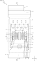
- FIG. 1 is a plan view of a semiconductor device according to a first embodiment of the present disclosure.
- FIG. 2 is a plan view corresponding to FIG. 1, seen through the sealing resin.
- FIG. 3 is a bottom view of the semiconductor device shown in FIG.
- FIG. 4 is a right side view of the semiconductor device shown in FIG.
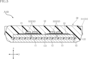
- FIG. 5 is a cross-sectional view taken along line VV in FIG.
- FIG. 6 is a cross-sectional view taken along line VI-VI in FIG.
- FIG. 7A is a partially enlarged view of FIG. 5, showing the first semiconductor element and its vicinity.
- FIG. 7B is a partially enlarged view of FIG. 5, showing the second semiconductor element and its vicinity.
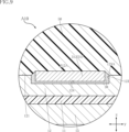
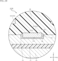
- FIG. 8 is a partially enlarged view of FIG. FIG.
- FIG. 9 is a cross-sectional view taken along line IX-IX in FIG.
- FIG. 10 is a partially enlarged cross-sectional view of a semiconductor device according to a first modified example of the first embodiment of the present disclosure.
- FIG. 11 is a partially enlarged cross-sectional view of a semiconductor device according to a second modified example of the first embodiment of the present disclosure.
- FIG. 12 is a partially enlarged cross-sectional view of a semiconductor device according to a third modified example of the first embodiment of the present disclosure.
- FIG. 13 is a partially enlarged cross-sectional view of a semiconductor device according to a fourth modified example of the first embodiment of the present disclosure.
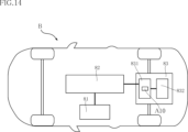
- FIG. 14 is a schematic diagram of a vehicle on which the semiconductor device shown in FIG. 1 is mounted.
- FIG. 14 is a schematic diagram of a vehicle on which the semiconductor device shown in FIG. 1 is mounted.
- FIG. 15 is a plan view of the semiconductor device according to the second embodiment of the present disclosure, seen through the sealing resin.
- FIG. 16 is a cross-sectional view taken along line XVI-XVI in FIG.
- FIG. 17 is a cross-sectional view taken along line XVII-XVII in FIG.
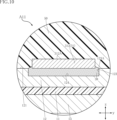
- FIG. 18 is a partially enlarged view of FIG.
- FIG. 19 is a cross-sectional view taken along line XIX-XIX in FIG.
- a semiconductor device A10 according to a first embodiment of the present disclosure will be described with reference to FIGS. 1 to 9.
- the semiconductor device A10 is generally used in a power conversion circuit such as an inverter.
- the semiconductor device A10 includes an insulating layer 11, a conductive layer 12, a heat dissipation layer 13, a first wiring layer 14, a first semiconductor element 21, a second semiconductor element 22, a first terminal 31, a second terminal 32, a first signal terminal 33, a second signal terminal 34, a first bonding layer 38, and a sealing resin 50.
- the semiconductor device A10 further includes a first conductive member 41, a second conductive member 42, and a third conductive member 43.
- FIG. 2 shows the sealing resin 50 through the sealing resin 50 for ease of understanding.
- the sealing resin 50 through the sealing resin 50 is shown by an imaginary line (two-dot chain line).
- first direction z the normal direction of the mounting surface 121 of the conductive layer 12 described below
- second direction x An example of a direction perpendicular to the first direction z
- third direction y A direction perpendicular to the first direction z and the second direction x will be referred to as the "third direction y.”
- the sealing resin 50 covers the first semiconductor element 21 and the second semiconductor element 22.
- the sealing resin 50 is an insulator.
- the sealing resin 50 is made of a material that contains, for example, black epoxy resin.
- the sealing resin 50 has a top surface 51, a bottom surface 52, a first side surface 53, and a second side surface 54.
- the top surface 51 faces the same side as the mounting surface 121 of the conductive layer 12, which will be described later, in the first direction z.
- the bottom surface 52 faces the opposite side to the top surface 51 in the first direction z.
- first side surface 53 and the second side surface 54 face in opposite directions in the second direction x.
- Each of the first side surface 53 and the second side surface 54 is connected to the top surface 51 and the bottom surface 52.
- the insulating layer 11 is covered with a sealing resin 50.
- the insulating layer 11 is made of a material having a relatively high thermal conductivity.
- the insulating layer 11 is made of a ceramic containing either silicon nitride ( Si3N4 ) or aluminum nitride (AlN).
- the insulating layer 11 may be made of a material containing resin.
- the conductive layer 12 is bonded to one side of the insulating layer 11 in the first direction z.
- the conductive layer 12 carries a first semiconductor element 21 and a second semiconductor element 22.
- the conductive layer 12 is surrounded by the periphery 111 of the insulating layer 11.
- the conductive layer 12 is covered with a sealing resin 50.
- the conductive layer 12 contains copper (Cu).
- the dimension of the conductive layer 12 in the first direction z is larger than the dimension of the insulating layer 11 in the first direction z.
- the conductive layer 12 has a mounting surface 121, a first end surface 122, and a plurality of first peripheral surfaces 123.
- the mounting surface 121 faces one side of the first direction z.
- the first semiconductor element 21 and the second semiconductor element 22 face the mounting surface 121.
- the first end surface 122 faces a direction perpendicular to the first direction z.
- the first end surface 122 is connected to the mounting surface 121.
- Each of the plurality of first peripheral surfaces 123 faces a direction perpendicular to the first direction z, and is located inward of the conductive layer 12 from the first end surface 122 when viewed in the first direction z.
- the plurality of first peripheral surfaces 123 are arranged along the third direction y. As shown in FIG. 9, each of the plurality of first peripheral surfaces 123 has a first upper edge 123A.
- the first upper edge 123A corresponds to the boundary between one of the multiple first peripheral surfaces 123 and the mounting surface 121.
- the conductive layer 12 is provided with a plurality of first engagement portions 124.
- the plurality of first engagement portions 124 are individually defined by a plurality of first peripheral surfaces 123.
- each of the plurality of first engagement portions 124 is a recess recessed from the mounting surface 121.
- the heat dissipation layer 13 is located on the opposite side of the insulating layer 11 from the conductive layer 12 and is joined to the insulating layer 11.
- the heat dissipation layer 13 is surrounded by the periphery 111 of the insulating layer 11 and overlaps the conductive layer 12.
- the heat dissipation layer 13 is exposed to the outside from the bottom surface 52 of the sealing resin 50.
- the heat dissipation layer 13 contains copper.
- the dimension of the heat dissipation layer 13 in the first direction z is larger than the dimension of the insulating layer 11 in the first direction z and is equal to the dimension of the conductive layer 12 in the first direction z.
- the relationship of the size of the heat dissipation layer 13 in the first direction z to the dimensions of the insulating layer 11 and the conductive layer 12 in the first direction z can be various.
- the first wiring layer 14 is located on the same side as the conductive layer 12 with respect to the insulating layer 11, and is bonded to the insulating layer 11.
- the first wiring layer 14 is located next to the conductive layer 12 in the second direction x.
- the first wiring layer 14 extends in the third direction y.
- the first wiring layer 14 is surrounded by the periphery 111 of the insulating layer 11.
- the first wiring layer 14 is covered with a sealing resin 50.
- the first wiring layer 14 contains copper.
- the dimension of the first wiring layer 14 in the first direction z is larger than the dimension of the insulating layer 11 in the first direction z.
- the first semiconductor element 21 is bonded to the mounting surface 121 of the conductive layer 12, as shown in Figures 5 and 6.
- the first semiconductor element 21 is, for example, a MOSFET (Metal-Oxide-Semiconductor Field-Effect Transistor).
- the first semiconductor element 21 may be a field effect transistor including a MISFET (Metal-Insulator-Semiconductor Field-Effect Transistor) or a bipolar transistor such as an IGBT (Insulated Gate Bipolar Transistor).
- the first semiconductor element 21 is an n-channel type MOSFET with a vertical structure.
- the first semiconductor element 21 includes a compound semiconductor substrate.
- the composition of the compound semiconductor substrate includes silicon carbide (SiC).
- the first semiconductor element 21 has a first electrode 211, two second electrodes 212, and a first gate electrode 213.
- the first electrode 211 is located on one side in the first direction z.
- the first electrode 211 faces the mounting surface 121 of the conductive layer 12.
- the first electrode 211 is conductively bonded to the mounting surface 121 via the conductive bonding layer 29. This allows the first electrode 211 to be electrically connected to the conductive layer 12.
- the conductive bonding layer 29 is, for example, solder.
- the conductive bonding layer 29 may be a sintered metal containing silver or the like.
- a current corresponding to the power before being converted by the first semiconductor element 21 flows through the first electrode 211.
- the first electrode 211 corresponds to the drain of the first semiconductor element 21.
- the two second electrodes 212 are located on the opposite side to the first electrode 211 in the first direction z. As shown in FIG. 2, the two second electrodes 212 are spaced apart from each other in the second direction x. A current corresponding to the power converted by the first semiconductor element 21 flows through each of the two second electrodes 212. In other words, the two second electrodes 212 correspond to the sources of the first semiconductor element 21.
- the first gate electrode 213 is located on the same side as the two second electrodes 212 in the first direction z.
- a gate voltage for driving the first semiconductor element 21 is applied to the first gate electrode 213.
- the first gate electrode 213 is conductive to the first wiring layer 14. As shown in FIG. 2, the area of the first gate electrode 213 is smaller than the area of each of the two second electrodes 212 when viewed in the first direction z.
- the second semiconductor element 22 is bonded to the mounting surface 121 of the conductive layer 12, as shown in FIG. 5.
- the second semiconductor element 22 is the same element as the first semiconductor element 21. Therefore, the second semiconductor element 22 is an n-channel type MOSFET with a vertical structure.
- the second semiconductor element 22 is located next to the first semiconductor element 21 in the third direction y.
- the second semiconductor element 22 has a third electrode 221, two fourth electrodes 222, and a second gate electrode 223.
- the third electrode 221 is located on one side in the first direction z.
- the third electrode 221 faces the mounting surface 121 of the conductive layer 12.
- the third electrode 221 is conductively bonded to the mounting surface 121 via the conductive bonding layer 29. This allows the third electrode 221 to be electrically connected to the conductive layer 12.
- a current corresponding to the power before being converted by the second semiconductor element 22 flows through the third electrode 221.
- the third electrode 221 corresponds to the drain of the second semiconductor element 22.
- the two fourth electrodes 222 are located on the opposite side to the third electrode 221 in the first direction z. As shown in FIG. 2, the two fourth electrodes 222 are spaced apart from each other in the second direction x. A current corresponding to the power converted by the second semiconductor element 22 flows through each of the two fourth electrodes 222. In other words, the two fourth electrodes 222 correspond to the sources of the second semiconductor element 22.
- the second gate electrode 223 is located on the same side as the two fourth electrodes 222 in the first direction z.
- a gate voltage for driving the second semiconductor element 22 is applied to the second gate electrode 223.
- the second gate electrode 223 is conductive to the first wiring layer 14. As shown in FIG. 2, the area of the second gate electrode 223 is smaller than the area of each of the two fourth electrodes 222 when viewed in the first direction z.
- the first terminal 31 is located on one side of the first semiconductor element 21 and the second semiconductor element 22 in the second direction x.
- the first terminal 31 is electrically connected to the first electrode 211 of the first semiconductor element 21 and the third electrode 221 of the second semiconductor element 22. Therefore, the first terminal 31 corresponds to the drain terminal of the semiconductor device A10.
- the first terminal 31 contains copper.
- the first terminal 31 has a first base 311 and a plurality of first bonding portions 312.
- the first base 311 is separated from the mounting surface 121 of the conductive layer 12.
- the first base 311 includes a portion covered with the sealing resin 50 and a portion exposed to the outside from the first side surface 53 of the sealing resin 50.
- the plurality of first bonding portions 312 extend from the first base 311 to the side where the first semiconductor element 21 and the second semiconductor element 22 are located in the second direction x.
- the plurality of first bonding portions 312 are arranged along the third direction y.
- Each of the plurality of first bonding portions 312 is covered with the sealing resin 50.
- the plurality of first bonding portions 312 individually overlap the plurality of first engagement portions 124 of the conductive layer 12.
- the first bonding layer 38 conductively bonds the multiple first engagement portions 124 of the conductive layer 12 to the multiple first bonding portions 312 of the first terminal 31 individually.
- the first terminal 31 is electrically connected to the first electrode 211 of the first semiconductor element 21 and the third electrode 221 of the second semiconductor element 22.
- the first bonding layer 38 is, for example, solder.
- each of the multiple first bonding portions 312 of the first terminal 31 is accommodated in one of the multiple first engagement portions 124 of the conductive layer 12.
- the first bonding layer 38 is in contact with the multiple first peripheral surfaces 123 of the conductive layer 12 that define each of the multiple first engagement portions 124. Furthermore, the first bonding layer 38 is in contact with the first upper edge 123A of each of the multiple first peripheral surfaces 123.
- each of the multiple first bonding portions 312 has a first upper surface 312A that faces the same side as the mounting surface 121 of the conductive layer 12 in the first direction z.
- the first bonding layer 38 is in contact with the edge of the first upper surface 312A.
- the second terminal 32 is conductively joined to the two second electrodes 212 of the first semiconductor element 21 and the two fourth electrodes 222 of the second semiconductor element 22. As a result, the second terminal 32 is electrically connected to each of the two second electrodes 212 and each of the two fourth electrodes 222. Therefore, the second terminal 32 corresponds to the source terminal of the semiconductor device A10.
- the second terminal 32 contains copper.
- the second terminal 32 has a second base 321, a plurality of second bonding portions 322, and a plurality of third bonding portions 323.
- the second base 321 overlaps the mounting surface 121 of the conductive layer 12.
- the second base 321 includes a portion covered with the sealing resin 50 and a portion exposed to the outside from the second side surface 54 of the sealing resin 50.
- Each of the plurality of second bonding portions 322 is connected to the second base 321 and covered with the sealing resin 50.
- each of the plurality of second bonding portions 322 protrudes from the second base 321 toward the first semiconductor element 21.
- Each of the plurality of second bonding portions 322 is conductively bonded to one of the two second electrodes 212 of the first semiconductor element 21 via the conductive bonding layer 29.
- Each of the multiple third bonding portions 323 is connected to the second base portion 321 and is covered with the sealing resin 50.
- Each of the multiple third bonding portions 323 protrudes from the second base portion 321 toward the second semiconductor element 22.
- Each of the multiple third bonding portions 323 is conductively bonded to one of the two fourth electrodes 222 of the second semiconductor element 22 via the conductive bonding layer 29.
- the first signal terminal 33 includes a portion covered by the sealing resin 50 and a portion exposed to the outside from the second side surface 54 of the sealing resin 50.
- the first signal terminal 33 is located on one side of the second base portion 321 of the second terminal 32 in the third direction y.
- the first signal terminal 33 is electrically connected to the first wiring layer 14. Therefore, the first signal terminal 33 is electrically connected to the first gate electrode 213 of the first semiconductor element 21 and the second gate electrode 223 of the second semiconductor element 22. In other words, the first signal terminal 33 corresponds to the gate terminal of the semiconductor device A10.
- the first signal terminal 33 includes copper.
- the portion of the first signal terminal 33 exposed to the outside from the second side surface 54 includes a portion extending along the first direction z.
- the second signal terminal 34 includes a portion covered by the sealing resin 50 and a portion exposed to the outside from the second side surface 54 of the sealing resin 50.
- the second signal terminal 34 is located between the first signal terminal 33 and the second base portion 321 of the second terminal 32 in the third direction y.
- the second signal terminal 34 is connected to the second base portion 321. Therefore, the second signal terminal 34 is electrically connected to each of the two second electrodes 212 and each of the two fourth electrodes 222.
- a voltage having the same potential as the voltage applied to each of the two second electrodes 212 and each of the two fourth electrodes 222 is applied to the second signal terminal 34.
- the second signal terminal 34 includes copper.
- the portion of the second signal terminal 34 exposed to the outside from the second side surface 54 includes a portion extending along the first direction z.
- the first conductive member 41 is conductively bonded to the first gate electrode 213 of the first semiconductor element 21 and the first wiring layer 14. This allows the first wiring layer 14 to be electrically connected to the first gate electrode 213.
- the first conductive member 41 is covered with a sealing resin 50.
- the first conductive member 41 is, for example, a wire containing either aluminum (Al) or gold (Au).
- the second conductive member 42 is conductively bonded to the second gate electrode 223 of the second semiconductor element 22 and the first wiring layer 14. This allows the first wiring layer 14 to be electrically connected to the second gate electrode 223.
- the second conductive member 42 is covered with a sealing resin 50.
- the second conductive member 42 is, for example, a wire containing either aluminum or gold.
- the third conductive member 43 is conductively bonded to the first wiring layer 14 and the first signal terminal 33. This allows the first wiring layer 14 to be electrically connected to the first signal terminal 33.
- the third conductive member 43 is covered with a sealing resin 50.
- the third conductive member 43 is, for example, a wire containing either aluminum or gold. In the semiconductor device A10, the third conductive member 43 is connected to the second conductive member 42.
- FIG. 10 The cross-sectional position of FIG. 10 is the same (or approximately the same) as the cross-sectional position of FIG. 9.
- each of the multiple first bonding portions 312 of the first terminal 31 is located outside each of the multiple first engagement portions 124 of the conductive layer 12.
- the first bonding layer 38 contacts the first upper edge 123A of each of the multiple first peripheral surfaces 123.
- the first bonding layer 38 is, for example, solder.
- FIG. 11 The cross-sectional position of FIG. 11 is the same (or approximately the same) as the cross-sectional position of FIG. 9.
- the entirety of each of the multiple first bonding portions 312 of the first terminal 31 is individually accommodated in the multiple first engagement portions 124 of the conductive layer 12. Furthermore, in the semiconductor device A12, at least one of the multiple first bonding portions 312 is in contact with one of the multiple first peripheral surfaces 123 that individually define the multiple first engagement portions 124. In the semiconductor device A12 as well, the first bonding layer 38 is in contact with the first upper edge 123A of each of the multiple first peripheral surfaces 123. Furthermore, the first bonding layer 38 is in contact with the edge of the first upper surface 312A of each of the multiple first bonding portions 312. The first bonding layer 38 is, for example, solder.
- FIG. 12 The cross-sectional position of FIG. 12 is the same (or approximately the same) as the cross-sectional position of FIG. 9.
- each of the multiple first engagement portions 124 is a slit that penetrates the conductive layer 12 in the first direction z.
- the first bonding layer 38 is in contact with the first upper edge 123A of each of the multiple first peripheral surfaces 123. Furthermore, the first bonding layer 38 is in contact with the edge of the first upper surface 312A of each of the multiple first bonding portions 312.
- the first bonding layer 38 is, for example, solder.
- FIG. 13 The cross-sectional position of FIG. 13 is the same (or approximately the same) as the cross-sectional position of FIG. 9.
- the vehicle B is, for example, an electric vehicle (EV).
- EV electric vehicle
- vehicle B is equipped with an on-board charger 81, a storage battery 82, and a drive system 83.
- Power is supplied to the on-board charger 81 wirelessly from a power supply facility (not shown) installed outdoors. Alternatively, power may be supplied from the power supply facility to the on-board charger 81 via a wired connection.
- the on-board charger 81 is configured with a step-up DC-DC converter. The voltage of the power supplied to the on-board charger 81 is stepped up by the converter and then supplied to the storage battery 82. The stepped-up voltage is, for example, 600V.
- the drive system 83 drives the vehicle B.
- the drive system 83 has an inverter 831 and a drive source 832.
- the semiconductor device A10 constitutes part of the inverter 831.
- the power stored in the storage battery 82 is supplied to the inverter 831.
- the power supplied from the storage battery 82 to the inverter 831 is DC power.
- a step-up DC-DC converter may be further provided between the storage battery 82 and the inverter 831.
- the inverter 831 converts DC power into AC power.
- the inverter 831 including the semiconductor device A10 is conducted to the drive source 832.
- the drive source 832 has an AC motor and a transmission.
- the AC motor rotates and the rotation is transmitted to the transmission.
- the transmission rotates the drive shaft of the vehicle B after appropriately reducing the rotation speed transmitted from the AC motor. This drives vehicle B.
- semiconductor device A10 in inverter 831 is necessary to output AC power with an appropriate frequency change to correspond to the required rotation speed of the AC motor.
- the semiconductor device A10 comprises a conductive layer 12 having a mounting surface 121, a first semiconductor element 21 bonded to the mounting surface 121, a first terminal 31 electrically connected to the first semiconductor element 21, and a first bonding layer 38 conductively bonding the conductive layer 12 and the first terminal 31.
- the conductive layer 12 is provided with a first engagement portion 124 defined by a first peripheral surface 123.
- the first terminal 31 has a first bonding portion 312 conductively bonded to the first engagement portion 124.
- the first bonding layer 38 conductively bonds the first engagement portion 124 and the first bonding portion 312. When viewed in the first direction z, the first bonding portion 312 overlaps the first engagement portion 124.
- the first bonding portion 312 remains in a position overlapping the first engagement portion 124 when viewed in the first direction z. Therefore, with this configuration, in the semiconductor device A10, it is possible to suppress the positional shift of the terminal with respect to the conductive layer 12.
- the first bonding layer 38 be in contact with the first peripheral surface 123 of the conductive layer 12. This is because this configuration is an indication of the large reaction force caused by the molten first bonding layer 38 from the first peripheral surface 123. Furthermore, it is preferable that the first bonding layer 38 be in contact with the first upper edge 123A of the first peripheral surface 123 of the conductive layer 12. This is because the surface tension generated in the molten first bonding layer 38 is further increased.
- the semiconductor device A10 At least a portion of the first bonding portion 312 of the first terminal 31 is housed in the first engagement portion 124.
- a larger reaction force is received from the first peripheral surface 123 of the conductive layer 12 via the molten first bonding layer 38, and the positional deviation of the first bonding portion 312 is restricted by the first peripheral surface 123. This effectively prevents the first terminal 31 from being misaligned relative to the conductive layer 12, and also prevents the first terminal 31 from rotating around the first direction z.
- the first bonding portion 312 of the first terminal 31 has a first upper surface 312A that faces the same side as the mounting surface 121 of the conductive layer 12 in the first direction z.
- the first bonding layer 38 is in contact with the edge of the first upper surface 312A. This configuration further increases the surface tension generated in the molten first bonding layer 38, thereby more effectively manifesting the self-alignment effect described above.
- the semiconductor device A10 further includes an insulating layer 11 to which a conductive layer 12 is bonded, and a heat dissipation layer 13 located on the opposite side of the insulating layer 11 from the conductive layer 12 and bonded to the insulating layer 11.
- the insulating layer 11 and the conductive layer 12 are covered with a sealing resin 50.
- the heat dissipation layer 13 is exposed to the outside from the sealing resin 50.
- the conductive layer 12 and the heat dissipation layer 13 are each spaced apart from the periphery 111 of the insulating layer 11.
- the vicinity of the periphery 111 of the insulating layer 11 is sandwiched between the sealing resin 50 on both sides in the first direction z. This makes it possible to prevent the insulating layer 11 and the conductive layer 12 from falling off from the sealing resin 50.
- each of the conductive layer 12 and the heat dissipation layer 13 in the first direction z is greater than the dimension of the insulating layer 11 in the first direction z. This configuration reduces the thermal resistance of each of the conductive layer 12 and the heat dissipation layer 13 in the first direction z. This can further improve the heat dissipation properties of the semiconductor device A10.
- FIG. 15 is seen through the sealing resin 50.
- the see-through sealing resin 50 is shown by imaginary lines.
- the semiconductor device A20 differs from the semiconductor device A10 in that it further includes a second wiring layer 15 and a second bonding layer 39, and in the configuration of the second terminal 32 and the second signal terminal 34.
- the second wiring layer 15 is located on the same side as the conductive layer 12 with respect to the insulating layer 11 as a reference, and is bonded to the insulating layer 11.
- the second wiring layer 15 is located between the conductive layer 12 and the first wiring layer 14 in the second direction x.
- the second wiring layer 15 extends in the third direction y.
- the second wiring layer 15 is surrounded by the periphery 111 of the insulating layer 11.
- the second wiring layer 15 is covered with a sealing resin 50.
- the second wiring layer 15 contains copper.
- the dimension of the second wiring layer 15 in the first direction z is larger than the dimension of the insulating layer 11 in the first direction z.
- the second wiring layer 15 has a second end surface 151 and a second peripheral surface 152.
- the second end surface 151 faces in a direction perpendicular to the first direction z.
- the second peripheral surface 152 faces in a direction perpendicular to the first direction z and is located inward of the second wiring layer 15 from the second end surface 151 when viewed in the first direction z.
- the second peripheral surface 152 has a second upper edge 152A.
- the second upper edge 152A corresponds to the boundary between the second peripheral surface 152 and the surface of the second wiring layer 15 that faces the same side as the mounting surface 121 of the conductive layer 12 in the first direction z.
- the second wiring layer 15 is provided with a second engagement portion 153.
- the second engagement portion 153 is defined by a second circumferential surface 152.
- the second engagement portion 153 is a recess that is recessed in the first direction z.
- the second terminal 32 has a support portion 324.
- the support portion 324 is connected to the second base portion 321 of the second terminal 32.
- the support portion 324 is covered with the sealing resin 50.
- the support portion 324 is located between the multiple second joint portions 322 of the second terminal 32 and the multiple third joint portions 323 of the second terminal 32.
- at least a portion of the support portion 324 is accommodated in the second engagement portion 153 of the second wiring layer 15.
- the second bonding layer 39 conductively bonds the second engagement portion 153 of the second wiring layer 15 to the support portion 324 of the second terminal 32.
- the second wiring layer 15 is electrically connected to each of the two second electrodes 212 of the first semiconductor element 21 and each of the two fourth electrodes 222 of the second semiconductor element 22.
- the second bonding layer 39 is, for example, solder.
- the second bonding layer 39 is in contact with the second peripheral surface 152 of the second wiring layer 15, which defines the second engagement portion 153 of the second wiring layer 15. Furthermore, the second bonding layer 39 is in contact with the second upper edge 152A of the second peripheral surface 152. As shown in FIGS. 18 and 19, the support portion 324 of the second terminal 32 has a second upper surface 324A that faces the same side as the mounting surface 121 of the conductive layer 12 in the first direction z. The second bonding layer 39 is in contact with the edge of the second upper surface 324A.
- the second signal terminal 34 is separated from the second terminal 32. As shown in FIG. 15 and FIG. 17, the second signal terminal 34 is conductively bonded to the second wiring layer 15 via the conductive bonding layer 29. This allows the second signal terminal 34 to be electrically connected to the second wiring layer 15.
- the semiconductor device A20 includes a conductive layer 12 having a mounting surface 121, a first semiconductor element 21 bonded to the mounting surface 121, a first terminal 31 electrically connected to the first semiconductor element 21, and a first bonding layer 38 conductively bonding the conductive layer 12 and the first terminal 31.
- the conductive layer 12 is provided with a first engaging portion 124 defined by a first peripheral surface 123.
- the first terminal 31 has a first bonding portion 312 conductively bonded to the first engaging portion 124.
- the first bonding layer 38 conductively bonds the first engaging portion 124 and the first bonding portion 312. When viewed in the first direction z, the first bonding portion 312 overlaps the first engaging portion 124. Therefore, according to this configuration, the semiconductor device A20 can also suppress misalignment of the terminal with respect to the conductive layer 12. Furthermore, the semiconductor device A20 has a configuration common to the semiconductor device A10, thereby achieving the same effects as the semiconductor device A10.
- the semiconductor device A20 further includes a second wiring layer 15 and a second bonding layer 39 that conductively bonds the second wiring layer 15 and the second terminal 32.
- the second wiring layer 15 is provided with a second engagement portion 153 defined by the second peripheral surface 152.
- the second terminal 32 has a support portion 324 that is conductively bonded to the second engagement portion 153 via the second bonding layer 39.
- the second bonding layer 39 is in contact with the second peripheral surface 152. At least a portion of the support portion 324 is accommodated in the second peripheral surface 152.
- the support portion 324 of the second terminal 32 is connected to the second base portion 321 of the second terminal 32. In a direction perpendicular to the first direction z, the support portion 324 is located between the second joint portion 322 and the third joint portion 323 of the second terminal 32.
- the conductive path length from the fourth electrode 222 of the second semiconductor element 22 to the second wiring layer 15 can be approximated to the conductive path length from the second electrode 212 of the first semiconductor element 21 to the second wiring layer 15.
- the conductive path length from the second signal terminal 34 to the fourth electrode 222 is approximately equal to the conductive path length from the second signal terminal 34 to the second electrode 212. Therefore, it is possible to suppress the resonance phenomenon accompanying the driving of each of the first semiconductor element 21 and the second semiconductor element 22.
- Appendix 1 a conductive layer having a mounting surface facing a first direction; a first semiconductor element bonded to the mounting surface; a first terminal electrically connected to the first semiconductor element; a first bonding layer that conductively bonds the conductive layer and the first terminal, the conductive layer has a first end surface facing a direction perpendicular to the first direction, and a first peripheral surface facing a direction perpendicular to the first direction and positioned inward of the conductive layer with respect to the first end surface as viewed in the first direction, the conductive layer is provided with a first engagement portion defined by the first circumferential surface, the first terminal has a first bonding portion that is conductively bonded to the first engagement portion via the first bonding layer, A semiconductor device, wherein when viewed in the first direction, the first joint portion overlaps the first engagement portion.
- Appendix 2 At least a portion of the first joint portion is accommodated in the first engagement portion, The semiconductor device according to claim 1, wherein the first bonding layer is in contact with the first peripheral surface.
- Appendix 3. the first terminal has a first base portion spaced from the mounting surface when viewed in the first direction; 3. The semiconductor device according to claim 2, wherein, when viewed in the first direction, the first joint portion extends from the first base portion toward a side on which the first semiconductor element is located in a direction perpendicular to the first direction.
- Appendix 4. the first joint portion has a first upper surface facing the same side as the mounting surface in the first direction, 4.
- Appendix 6. The semiconductor device according to claim 3 or 4, wherein the first engagement portion includes a recess recessed from the mounting surface. Appendix 7. 5. The semiconductor device according to claim 3, wherein the first engagement portion includes a slit penetrating the conductive layer.
- Appendix 8. the first semiconductor element has a first electrode and a second electrode positioned opposite to each other in the first direction; 5. The semiconductor device according to claim 3, wherein the first electrode is conductively connected to the mounting surface.
- Appendix 9. 9. The semiconductor device of claim 8, further comprising a second terminal conductively connected to the second electrode.
- a first wiring layer is further provided, the first semiconductor element has a first gate electrode located on the same side as the second electrode in the first direction; 10.
- Appendix 11. a first signal terminal electrically connected to the first wiring layer; a sealing resin that covers the first semiconductor element, 11.
- each of the first base portion and the first signal terminal includes a portion exposed to the outside from the sealing resin.
- Appendix 12. Further comprising an insulating layer; the conductive layer and the first wiring layer are bonded to a side of the insulating layer facing the mounting surface in the first direction, 12.
- the semiconductor device wherein, when viewed in the first direction, the conductive layer and the first wiring layer are each spaced apart from a periphery of the insulating layer.
- Appendix 13 a heat dissipation layer located on the opposite side of the insulating layer from the conductive layer and bonded to the insulating layer; When viewed in the first direction, the heat dissipation layer is spaced apart from a periphery of the insulating layer, the insulating layer and the conductive layer are covered with the sealing resin, 13.
- Appendix 14. 14 14.
- the semiconductor device wherein at least a portion of the support portion is accommodated in the second engagement portion.
- Appendix 16 a second semiconductor element having a third electrode and a fourth electrode positioned opposite to each other in the first direction and covered with the sealing resin; the third electrode is conductively connected to the mounting surface; the second terminal has a second base portion including a portion exposed to the outside from the sealing resin, a second joint portion connected to the second base portion and conductively joined to the second electrode, and a third joint portion connected to the second base portion and conductively joined to the fourth electrode,
- the support portion is connected to the second base portion, 16.
- the semiconductor device according to claim 15, wherein the support portion is located between the second joint portion and the third joint portion in a direction perpendicular to the first direction.
- Appendix 17 a second signal terminal electrically connected to the second wiring layer; 17.
- Appendix 18. A driving source;
Landscapes
- Structures Or Materials For Encapsulating Or Coating Semiconductor Devices Or Solid State Devices (AREA)
- Chemical & Material Sciences (AREA)
- Engineering & Computer Science (AREA)
- Ceramic Engineering (AREA)
Priority Applications (4)
| Application Number | Priority Date | Filing Date | Title |
|---|---|---|---|
| CN202480012147.4A CN120712648A (zh) | 2023-02-20 | 2024-01-29 | 半导体装置以及车辆 |
| JP2025502202A JPWO2024176740A1 (https=) | 2023-02-20 | 2024-01-29 | |
| DE112024000604.3T DE112024000604T5 (de) | 2023-02-20 | 2024-01-29 | Halbleiterbauteil und fahrzeug |
| US19/298,853 US20250374649A1 (en) | 2023-02-20 | 2025-08-13 | Semiconductor device and vehicle |
Applications Claiming Priority (2)
| Application Number | Priority Date | Filing Date | Title |
|---|---|---|---|
| JP2023-024454 | 2023-02-20 | ||
| JP2023024454 | 2023-02-20 |
Related Child Applications (1)
| Application Number | Title | Priority Date | Filing Date |
|---|---|---|---|
| US19/298,853 Continuation US20250374649A1 (en) | 2023-02-20 | 2025-08-13 | Semiconductor device and vehicle |
Publications (1)
| Publication Number | Publication Date |
|---|---|
| WO2024176740A1 true WO2024176740A1 (ja) | 2024-08-29 |
Family
ID=92500752
Family Applications (1)
| Application Number | Title | Priority Date | Filing Date |
|---|---|---|---|
| PCT/JP2024/002597 Ceased WO2024176740A1 (ja) | 2023-02-20 | 2024-01-29 | 半導体装置および車両 |
Country Status (5)
| Country | Link |
|---|---|
| US (1) | US20250374649A1 (https=) |
| JP (1) | JPWO2024176740A1 (https=) |
| CN (1) | CN120712648A (https=) |
| DE (1) | DE112024000604T5 (https=) |
| WO (1) | WO2024176740A1 (https=) |
Cited By (1)
| Publication number | Priority date | Publication date | Assignee | Title |
|---|---|---|---|---|
| WO2026053967A1 (ja) * | 2024-09-09 | 2026-03-12 | ローム株式会社 | 半導体モジュール |
Citations (3)
| Publication number | Priority date | Publication date | Assignee | Title |
|---|---|---|---|---|
| US4994412A (en) * | 1990-02-09 | 1991-02-19 | Motorola Inc. | Self-centering electrode for power devices |
| JPH09283653A (ja) * | 1996-04-17 | 1997-10-31 | Nec Corp | 半導体容器 |
| WO2024018790A1 (ja) * | 2022-07-19 | 2024-01-25 | ローム株式会社 | 半導体装置 |
-
2024
- 2024-01-29 WO PCT/JP2024/002597 patent/WO2024176740A1/ja not_active Ceased
- 2024-01-29 JP JP2025502202A patent/JPWO2024176740A1/ja active Pending
- 2024-01-29 DE DE112024000604.3T patent/DE112024000604T5/de active Pending
- 2024-01-29 CN CN202480012147.4A patent/CN120712648A/zh active Pending
-
2025
- 2025-08-13 US US19/298,853 patent/US20250374649A1/en active Pending
Patent Citations (3)
| Publication number | Priority date | Publication date | Assignee | Title |
|---|---|---|---|---|
| US4994412A (en) * | 1990-02-09 | 1991-02-19 | Motorola Inc. | Self-centering electrode for power devices |
| JPH09283653A (ja) * | 1996-04-17 | 1997-10-31 | Nec Corp | 半導体容器 |
| WO2024018790A1 (ja) * | 2022-07-19 | 2024-01-25 | ローム株式会社 | 半導体装置 |
Cited By (1)
| Publication number | Priority date | Publication date | Assignee | Title |
|---|---|---|---|---|
| WO2026053967A1 (ja) * | 2024-09-09 | 2026-03-12 | ローム株式会社 | 半導体モジュール |
Also Published As
| Publication number | Publication date |
|---|---|
| DE112024000604T5 (de) | 2025-11-20 |
| US20250374649A1 (en) | 2025-12-04 |
| CN120712648A (zh) | 2025-09-26 |
| JPWO2024176740A1 (https=) | 2024-08-29 |
Similar Documents
| Publication | Publication Date | Title |
|---|---|---|
| JP6897869B2 (ja) | 半導体モジュール | |
| US20250374649A1 (en) | Semiconductor device and vehicle | |
| US20250372511A1 (en) | Semiconductor device and vehicle | |
| WO2023112662A1 (ja) | 半導体モジュールおよび半導体装置 | |
| WO2025142335A1 (ja) | 半導体装置 | |
| WO2023149257A1 (ja) | 半導体装置 | |
| WO2023190180A1 (ja) | 半導体装置 | |
| US20250338597A1 (en) | Semiconductor device and vehicle | |
| US20260053054A1 (en) | Semiconductor device, method for manufacturing semiconductor device, and vehicle | |
| WO2025177840A1 (ja) | 半導体装置および車両 | |
| JP2024175866A (ja) | 半導体装置、半導体装置の製造方法、および車両 | |
| WO2024162052A1 (ja) | 半導体装置および車両 | |
| WO2025109999A1 (ja) | 半導体装置、半導体モジュールおよび車両 | |
| JP2025098863A (ja) | 半導体装置および車両 | |
| US20240282681A1 (en) | Semiconductor device, and semiconductor device mounting body | |
| WO2025158862A1 (ja) | 半導体装置および車両 | |
| JP2024157347A (ja) | 半導体装置、半導体装置の製造方法、および車両 | |
| WO2025004780A1 (ja) | 半導体装置、半導体モジュールおよび車両 | |
| WO2024262343A1 (ja) | 半導体装置および半導体モジュール | |
| WO2025121140A1 (ja) | 半導体装置、半導体装置の製造方法、インバータ装置および車両 | |
| WO2025216041A1 (ja) | 半導体装置およびインバータシステム | |
| WO2024228322A1 (ja) | 半導体装置 | |
| JP2025185284A (ja) | 半導体装置および半導体モジュール | |
| WO2025249259A1 (ja) | 半導体装置 | |
| WO2026042579A1 (ja) | 半導体装置 |
Legal Events
| Date | Code | Title | Description |
|---|---|---|---|
| 121 | Ep: the epo has been informed by wipo that ep was designated in this application |
Ref document number: 24760047 Country of ref document: EP Kind code of ref document: A1 |
|
| ENP | Entry into the national phase |
Ref document number: 2025502202 Country of ref document: JP Kind code of ref document: A |
|
| WWE | Wipo information: entry into national phase |
Ref document number: 2025502202 Country of ref document: JP |
|
| WWE | Wipo information: entry into national phase |
Ref document number: 112024000604 Country of ref document: DE |
|
| 122 | Ep: pct application non-entry in european phase |
Ref document number: 24760047 Country of ref document: EP Kind code of ref document: A1 |