WO2024176584A1 - 窒素-空孔複合欠陥を有する材料の製造方法、製造装置、製造プログラム、及び窒素-空孔複合欠陥を有する材料 - Google Patents
窒素-空孔複合欠陥を有する材料の製造方法、製造装置、製造プログラム、及び窒素-空孔複合欠陥を有する材料 Download PDFInfo
- Publication number
- WO2024176584A1 WO2024176584A1 PCT/JP2023/045056 JP2023045056W WO2024176584A1 WO 2024176584 A1 WO2024176584 A1 WO 2024176584A1 JP 2023045056 W JP2023045056 W JP 2023045056W WO 2024176584 A1 WO2024176584 A1 WO 2024176584A1
- Authority
- WO
- WIPO (PCT)
- Prior art keywords
- electron beam
- manufacturing
- heat treatment
- beam irradiation
- hetero element
- Prior art date
- Legal status (The legal status is an assumption and is not a legal conclusion. Google has not performed a legal analysis and makes no representation as to the accuracy of the status listed.)
- Ceased
Links
Images







Classifications
-
- C—CHEMISTRY; METALLURGY
- C01—INORGANIC CHEMISTRY
- C01B—NON-METALLIC ELEMENTS; COMPOUNDS THEREOF; METALLOIDS OR COMPOUNDS THEREOF NOT COVERED BY SUBCLASS C01C
- C01B32/00—Carbon; Compounds thereof
- C01B32/25—Diamond
- C01B32/28—After-treatment, e.g. purification, irradiation, separation or recovery
-
- C—CHEMISTRY; METALLURGY
- C30—CRYSTAL GROWTH
- C30B—SINGLE-CRYSTAL GROWTH; UNIDIRECTIONAL SOLIDIFICATION OF EUTECTIC MATERIAL OR UNIDIRECTIONAL DEMIXING OF EUTECTOID MATERIAL; REFINING BY ZONE-MELTING OF MATERIAL; PRODUCTION OF A HOMOGENEOUS POLYCRYSTALLINE MATERIAL WITH DEFINED STRUCTURE; SINGLE CRYSTALS OR HOMOGENEOUS POLYCRYSTALLINE MATERIAL WITH DEFINED STRUCTURE; AFTER-TREATMENT OF SINGLE CRYSTALS OR A HOMOGENEOUS POLYCRYSTALLINE MATERIAL WITH DEFINED STRUCTURE; APPARATUS THEREFOR
- C30B29/00—Single crystals or homogeneous polycrystalline material with defined structure characterised by the material or by their shape
- C30B29/02—Elements
- C30B29/04—Diamond
Definitions
- the present invention relates to a method, an apparatus, and a program for manufacturing a material having a nitrogen-vacancy complex defect, and to a material having a nitrogen-vacancy complex defect.
- NV centers nitrogen-vacancy complex defects
- diamonds that have NV centers inside them can be used to measure temperature, pH, electric fields, magnetic fields, etc.
- Non-Patent Document 1 discloses a technique for forming NV centers in synthetic diamond by irradiating the synthetic diamond with an electron beam.
- An object of one aspect of the present invention is to realize a method for producing a material having an NV center that achieves a high concentration of hetero element-vacancy complex defects by suppressing the accumulation and increase of significant defects and strain in the material.
- a manufacturing method is a method for manufacturing a material having a hetero element-vacancy complex defect, and includes a preparation step of preparing a material containing a hetero element as an impurity, an electron beam irradiation step of irradiating the material with an electron beam to form vacancies in the material, and a heat treatment step of heating the material irradiated with the electron beam to form nitrogen-vacancy complex defects in the material, and the electron beam irradiation step and the heat treatment step are repeated alternately two or more times.
- a method for manufacturing a material having an NV center that achieves a high concentration of heteroelement-vacancy complex defects while suppressing the accumulation and increase of significant defects and strain in the material.
- FIG. 1 is a diagram showing a configuration of a manufacturing apparatus according to an embodiment of the present invention.
- FIG. 2 is a flow diagram illustrating an example manufacturing process according to an embodiment of the present invention.
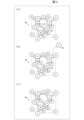
- FIG. 2 is a schematic enlarged view showing an example of a material used in a manufacturing process according to an embodiment of the present invention.
- FIG. 2 is a diagram showing a fluorescence spectrum of a material produced by the production process according to Example 1.
- 1 is a diagram showing the relationship between the fluorescence intensity of the material produced by the production process according to Example 1 and the total amount of electron irradiation.
- FIG. FIG. 13 is a diagram showing the fluorescence spectrum of the material produced by the production process according to Example 2.
- FIG. 1 is a diagram showing a configuration of a manufacturing apparatus according to an embodiment of the present invention.
- FIG. 2 is a flow diagram illustrating an example manufacturing process according to an embodiment of the present invention.
- FIG. 2 is a schematic enlarged view showing an example of a material used
- FIG. 13 is a diagram showing the relationship between the fluorescence intensity and the total amount of electron irradiation of the material produced by the production process according to Example 2.
- FIG. 1 is a diagram showing a measurement device for ODMR.
- FIG. 13 is a diagram showing the results of ODMR measurement of a material produced by the production process according to Example 2.
- FIG. 13 is a diagram showing the relationship between the contrast of the ODMR signal of the material manufactured by the manufacturing process according to the second embodiment and the total electron irradiation dose.
- 13 is a diagram showing the relationship between the fluorescence intensity and the contrast of the ODMR signal of the material produced by the production process according to Example 2 and the total amount of electron irradiation.
- FIG. 1 is a diagram showing a measurement device for ODMR.
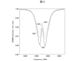
- FIG. 13 is a diagram showing the results of ODMR measurement of a material produced by the production process according to Example 2.
- FIG. 13 is a diagram showing the relationship between the contrast of the ODMR signal of the
- FIG. 1 is a diagram showing the configuration of a manufacturing apparatus 10 according to an embodiment of the present invention.
- the manufacturing apparatus 10 has a mounting section 11, an electron beam irradiation section 12, a heat treatment section 13, and a control section 14, and forms a hetero element-vacancy complex defect (as an example, a nitrogen-vacancy complex defect: NV center) in the material M.
- a hetero element means an element other than carbon and hydrogen, for example, nitrogen (N), silicon (Si), and germanium (Ge).
- examples of hetero element-vacancy complex defects include a nitrogen-vacancy complex defect (NV center), a silicon-vacancy complex defect (SiV center), and a germanium-vacancy complex defect (GeV center).
- the material M is a material containing a hetero element (for example, nitrogen) as an impurity, for example, synthetic diamond, or a fine particle of synthetic diamond.
- Synthetic diamond can be produced, for example, by high pressure and high temperature (HPHT), chemical vapor deposition (CVD), or detonation, and it is relatively easy to control the composition, concentration, crystal distortion, size, shape, etc. of the impurities.
- Synthetic diamond contains nitrogen as an impurity, for example, at a concentration of about 100 ppm.
- the following description uses nitrogen as an example of a hetero element, but a material containing a SiV center or a GeV center may be produced using the material M containing a hetero element other than nitrogen, for example, silicon or germanium, as an impurity.
- the synthetic diamond particles have a roughly crushed stone shape (like crushed stone) with a diameter of, for example, about 5 nm to about 1000 nm (50 nm as an example).
- the mounting unit 11 is a table on which the material M is placed when the material M is irradiated with the electron beam EB.
- the mounting unit 11 can function as a cooling table, using its heat capacity, to cool the material M that is heated by the irradiation of the electron beam.
- the mounting section 11 is preferably conductive to prevent charging due to irradiation with the electron beam EB.
- the material M is mounted on the mounting section 11 directly or indirectly via a conductive boat or the like. If the material M is fine particles (powder), the material M is preferably wrapped in a thin film of a conductive material, such as aluminum, platinum, gold, etc. (aluminum foil is one example) and then mounted on the mounting section 11. This is to prevent the material M from scattering.
- the electron beam irradiating unit 12 accelerates electrons and irradiates them as an electron beam EB to the material M.
- the electrons are accelerated to, for example, 2 MeV, and irradiated with an electron current of, for example, 6 mA at a dose of, for example, 1*10 17 to 1*10 19 cm ⁇ 2 per irradiation.
- the heat treatment section 13 holds the material M after irradiation with the electron beam EB in an internal space, here, inside a heat-resistant tube CT (e.g., inside an alumina tube), and performs heat treatment. At this time, the material M is held in a heat-resistant container, for example, an alumina port, and is held in the internal space of the heat treatment section 13.
- a heat-resistant tube CT e.g., inside an alumina tube
- the manufacturing device 10 may have a camera for checking the material M, and a manipulator for placing the material M on the placement section 11 and moving the material M irradiated with the electron beam from the placement section 11 to the heat treatment section 13.
- the control unit 14 has a processor 141, a primary memory 142, a secondary memory 143, an input/output interface 144, and a bus 145.
- the processor 141, the primary memory 142, the secondary memory 143, and the input/output interface 144 are interconnected via the bus 145.
- the manufacturing program P1 is stored (non-volatile memory) in the secondary memory 143.
- the processor 141 expands the manufacturing program P1 stored in the secondary memory 143 onto the primary memory 142.
- the processor 141 controls the electron beam irradiation unit 12 and the heat treatment unit 13 (and possibly the manipulator) according to the instructions contained in the manufacturing program P1 expanded onto the primary memory 142, to execute each step (steps S12, S13, S14) included in the manufacturing process described below.
- An example of a device that can be used as the processor 141 is a CPU (Central Processing Unit).
- An example of a device that can be used as the primary memory 142 is a semiconductor RAM (Random Access Memory).
- An example of a device that can be used as the secondary memory 143 is a HDD (Hard Disk Drive).
- An input device and/or an output device are connected to the input/output interface 144.
- An example of an input device connected to the input/output interface 144 is a camera for checking the material M.
- Output devices connected to the input/output interface 144 include the electron beam irradiation unit 12, the heat treatment unit 13, a manipulator, etc.
- Interfaces that can be used as the input/output interface 144 include, for example, a PCI (Peripheral Component Interconnect) interface and a USB (Universal Serial Bus).
- PCI Peripheral Component Interconnect
- USB Universal Serial Bus
- the manufacturing program P1 may be recorded on a computer-readable, non-transitory, tangible recording medium.
- This recording medium may be the secondary memory 143 or another recording medium.
- a tape, a disk, a card, a semiconductor memory, a programmable logic circuit, etc. may be used as the other recording medium.
- FIG. 2 is a flow diagram showing an example of a manufacturing process according to an embodiment of the present invention.
- Fig. 3 is an enlarged view showing an example of a material M used in the manufacturing process according to an embodiment of the present invention. The manufacturing process will be described below with reference to Fig. 2.
- Step S11 Preparation step of preparing material M containing nitrogen
- the material M is a material containing nitrogen, for example, synthetic diamond (one example is fine particles of synthetic diamond) (see FIG. 3A).
- synthetic diamond contains nitrogen (N) as an impurity.
- material M preferably contains 5 atomic ppm or more and 3000 atomic ppm or less of nitrogen, and more preferably 50 atomic ppm or more and 1000 atomic ppm or less of nitrogen (100 atomic ppm as an example).
- Sensors, etc. preferably have 1 atomic ppm or more of NV centers, and more preferably have 10 atomic ppm or more of NV centers.
- a relatively high concentration of nitrogen impurities facilitates the formation of NV centers, while a concentration of nitrogen impurities that is too high can cause the characteristics (e.g., sensitivity) of sensors, etc. to deteriorate.
- the average particle size of the microparticles is preferably 5 nm or more, and more preferably 10 nm or more (for example, 50 nm). This is because the efficiency of forming NV centers during the heat treatment process decreases in diamond microparticles with an excessively small particle size.
- NDs with an average particle size of 50 nm can be used.
- the average particle size of the microparticles is measured by dynamic light scattering.
- step S12 electron beam irradiation step of irradiating the material M with an electron beam EB to form voids V in the material M
- the material M is placed on the placement portion 11 and irradiated with an electron beam.
- a part (C1) of the carbon C in the material M is removed from the lattice, and a vacancy V is formed (see FIG. 3B).
- the electrons it is preferable to accelerate the electrons to 300 keV or more and 3 MeV or less (for example, 2 MeV). This is to introduce vacancies V uniformly throughout the material M.
- the dose of electrons irradiated to the material M is preferably 1*10 12 cm -2 or more and 1*10 19 cm -2 or less (4*10 18 cm -2 as one example).
- the dose is preferably 1*10 12 cm -2 or more and 1*10 19 cm -2 or less (4*10 18 cm -2 as one example).
- efficient NV coupling can be promoted during the subsequent heat treatment.
- the concentration of the generated vacancies V can be made to correspond to the concentration of nitrogen impurities contained in the material M, and NV coupling can be generated efficiently.
- the electron beam irradiation can be performed at room temperature (e.g., room temperature) in the atmosphere, but may also be performed, for example, under reduced pressure (or inert gas flow) or under heating. Of these, under reduced pressure (or inert gas flow) and heating is preferred. By simultaneously performing electron beam irradiation and heating, it becomes possible to introduce vacancies V and form NV more efficiently than when heating is not performed during electron beam irradiation.
- the material M is a powder made up of fine particles with a diameter of 1 ⁇ m or less, it is preferable that the material M is covered with a conductive material before the electron beam is irradiated. This is to prevent the material M from scattering.
- the conductive material is, for example, a thin film of aluminum, platinum, gold, etc. (one example is aluminum foil).
- Step S13 a heat treatment process for heating the material M irradiated with the electron beam EB to form nitrogen-vacancy complex defects (NV centers) in the material M
- the material M in which the vacancies V have been formed is heated to move the vacancies V.
- an NV center is formed in which nitrogen N is bonded to the vacancies V (see FIG. 3(c)).
- the vacancies V in diamond move about 46 nm (thermal diffusion length) by heat treatment at 900° C. for 2 hours, and bond with nitrogen in the diamond.
- the vacancies V move to the position of carbon C in C2, and an NV center is formed.
- the heat treatment process (step S13) preferably includes a heating step in which the temperature of material M is maintained at 400°C or higher and 1400°C or lower for 1 second or longer and 12 hours or shorter, and more preferably, in this heating step, the temperature of material M is maintained at 700°C or higher and 1100°C or lower (e.g., 900°C) for 1 hour or longer and 5 hours or shorter (e.g., 2 hours).
- the formation of NV centers requires atomic rearrangement by high-temperature heat treatment. On the other hand, excessively high temperatures or long heat treatments can cause adverse effects such as graphitization of material M (diamond) and the formation of complex defects other than NV centers in material M.
- the heat treatment process may include a cooling process for cooling the material M heated by the heating process, and a process for holding the material M cooled by the cooling process at a temperature of 300°C or more and 800°C or less (for example, 575°C) in an oxygen atmosphere (for example, in air) for 1 minute or more and 24 hours or less (for example, 3 hours) to form an oxide film on the material M.
- a temperature of 300°C or more and 800°C or less for example, 575°C
- an oxygen atmosphere for example, in air
- 1 minute or more and 24 hours or less for example, 3 hours
- step S14 a step in which the electron beam irradiation step and the heat treatment step are alternately repeated two or more times
- the electron beam irradiation and heat treatment in steps S12 and S13 are repeated until the number of repetitions n reaches a predetermined value of 2 or more.
- the total dose of electrons irradiated to the material M is preferably 1*10 12 cm -2 or more and 1*10 19 cm -2 or less (4*10 18 cm -2 as one example).
- the concentration of vacancies V generated by an irradiation dose in this range corresponds to the concentration of nitrogen impurities in the material M, and enables efficient NV coupling to be formed between the vacancies V and the nitrogen impurities.
- the above manufacturing process results in the formation of a sample with NV centers.
- heteroelement-vacancy complex defects e.g., NV centers
- materials having heteroelement-vacancy complex defects emit fluorescence, and the amount of fluorescence changes with the application of microwaves, etc. For example, when green light is irradiated onto a material having an NV center, red light is emitted as reflected light.
- microwaves of, for example, a wavelength of 2.8 GHz are applied to a material having an NV center, the amount of fluorescence (red light) (emission intensity) decreases.
- materials having heteroelement-vacancy complex defects can be used in sensors (quantum metrology, sensing).
- the heteroelement-vacancy complex defects e.g., NV centers
- the heteroelement-vacancy complex defects can be concentrated while suppressing an increase in defects and distortion in the material M, thereby increasing the sensitivity of sensors using heteroelement-vacancy complex defects.
- Example 1 Hereinafter, Example 1 will be described. ND having an average particle size of 50 nm was used as the material M. This is common to Examples 1 and 2.
- Example 1 the electron beam irradiation and heat treatment were repeated.
- the energy of the irradiated electrons was 2 MeV
- the amount of electron beam irradiation per time was constant (2*10 18 cm -2 )
- the total amount of electron beam irradiation was changed up to 1*10 19 cm -2 .
- the electron beam irradiation and heat treatment were performed only once and were not repeated.
- the energy of the irradiated electrons was 2 MeV, and the amount of electron beam irradiation was changed from 2*10 18 cm -2 .
- the electron beam irradiation was performed at room temperature, and the heat treatment was performed at 900° C. for 2 hours.
- FIG. 4 is a diagram showing the fluorescence spectrum of a material produced by a production process according to one embodiment of the present invention.
- Graphs G11 to G13 show the fluorescence spectrum when the total electron dose is 4*10 18 , 6*10 18 , and 8*10 18 cm -2 .
- Graphs G11 to G13 show a fluorescence peak FL1 at 575 nm caused by NV 0 (uncharged NV center) and a fluorescence peak FL2 at 637 nm caused by NV - (negatively charged NV center).
- a light source having a pulse height wavelength of 532 nm HORIBA LabRAM HR Evolution/Excitation light in this case was used as the light source.
- FIG. 5 is a graph showing the relationship between the fluorescence intensity of the material produced by the manufacturing process of Example 1 and the total amount of electron irradiation.
- Graph G21 corresponds to Example 1
- graph G20 corresponds to the comparative example.
- Example 1 the fluorescence intensity tended to increase with increasing dose of electron beam.
- the fluorescence intensity was 300 times higher than that of the unirradiated case.
- the fluorescence intensity increased linearly with the dose up to a dose of 4*10 18 cm -2 , but decreased as the dose increased further.
- Example 1 it can be considered that irradiation with electrons of more than 4*10 18 cm -2 tends to inhibit the coupling (formation of NV centers) between vacancies (defects) and nitrogen in material M.
- material M is annealed to form NV centers every time electrons of 2*10 18 cm -2 are irradiated.
- NV centers do not couple at once, and coupling is reliably formed by NV annealing after each irradiation.
- Example 1 although the emission intensity is inferior to that of continuous irradiation up to 2*10 18 to 6*10 18 cm -2 , the emission intensity is still high even when the irradiation reaches a high dose.
- the emission intensity can be increased by alternately irradiating the electron beam and performing heat treatment.
- the fluorescence intensity can be increased by 300% or more compared to a sample not irradiated with the electron beam.
- the sample can be produced in a short time compared to the case of irradiating a fixed amount at a time by continuous irradiation, and the emission intensity can be increased efficiently (emission intensity of more than 200% compared to unirradiated).
- Example 2 In Example 2, electron beam irradiation and heat treatment were repeated. The energy of the irradiated electrons was 2 MeV, the amount of electron beam irradiation per time was constant (1*10 18 cm -2 ), and the total amount of electron beam irradiation was changed up to 7*10 18 cm -2 . The electron beam irradiation was performed at room temperature, and the heat treatment was performed at 900° C. for 2 hours.
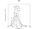
- FIG. 6 is a diagram showing the fluorescence spectrum of the material produced by the production process according to Example 2.
- Graphs G51 to G57 show the fluorescence spectrum of Example 2 when the total electron irradiation dose is 0 to 7*10 18 cm -2 .
- Graphs G11 to G13 show the fluorescence peak FL1 at 575 nm caused by NV 0 and the fluorescence peak FL2 at 637 nm caused by NV - . Note that the light source used was the same as that of Example 1, having a pulse height wavelength of 532 nm.
- FIG. 7 shows the relationship between the fluorescence intensity of the material produced by the manufacturing process of Example 2 and the total amount of electron irradiation.
- Graph G6 corresponds to Example 2.
- FIG 8 is a diagram showing an ODMR (optically detected magnetic resonance) measuring device.
- the measuring device has a laser light source 21, a dichroic mirror 22, an objective lens 23, a filter 24, a camera 25, a microwave signal generator 26, a microwave oscillation antenna 27, and an I/O 28.
- the laser light L1 emitted from the laser light source 21 is reflected by the mirror 22, collected by the objective lens 23, and enters the measurement object OB, i.e., the sample in which the NV center is formed.
- the fluorescence L2 from the measurement object OB passes through the dichroic mirror 22 and the filter 24 and enters the camera 25.
- the microwave signal generator 26 generates a microwave signal P.
- the microwave oscillation antenna 27 irradiates the measurement object OB with microwaves based on this signal P.
- the camera 25 is synchronized with the microwave modulation and frequency sweep by the microwave signal generator 26 via the I/O 28. As a result, the change in fluorescence intensity relative to the microwave frequency can be obtained as the contrast of the ODMR signal.
- the contrast of an ODMR (optically detected magnetic resonance) signal can be defined as the absolute value of the maximum rate of change of fluorescence intensity in the ODMR signal.
- the ODMR signal is a plot of the ratio of the fluorescence intensity when microwaves are applied to the fluorescence intensity when no microwaves are applied, versus the microwave frequency.
- the ODMR signal can be obtained by detecting the fluorescence from the OB to be measured while applying microwaves with a frequency sweep to the OB to be measured.
- the ODMR signal is acquired under the following conditions: (1) the wavelength of the excitation light source used to generate fluorescence is 532 nm; (2) a 1.5-turn coil with a diameter of 5 mm is used to apply microwaves to the OB to be measured, and the frequency sweep width of the microwaves is 2.83 GHz to 2.91 GHz; the microwave intensity is 10 mW to 10 W, and the excitation light intensity is 300 W/ cm2 to 3 MW/ cm2 , at which the contrast of the ODMR signal is maximized.
- Graphs G91 to G94 are graphs corresponding to total electron beam irradiation doses of 2*10 18 , 4*10 18 , 6*10 18 , and 7*10 18 cm ⁇ 2 .
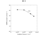
- FIG. 10 is a diagram showing the relationship between the contrast of the ODMR signal of the material produced by the manufacturing process of Example 2 and the total amount of electron irradiation.
- FIG. 11 is a diagram showing the relationship between the fluorescence intensity and the contrast of the ODMR signal of the material produced by the manufacturing process of Example 2 and the total amount of electron irradiation.
- the intensity of the fluorescence, the concentration of NV ⁇ , and the contrast of the ODMR signal change depending on the dose of electron beam irradiation.
- the manufacturing method of the first aspect is a manufacturing method of a material having a hetero element-vacancy complex defect, and includes a preparation step of preparing a material containing a hetero element as an impurity, an electron beam irradiation step of irradiating the material with an electron beam to form vacancies in the material, and a heat treatment step of heating the material irradiated with the electron beam to form hetero element-vacancy complex defects in the material, the electron beam irradiation step and the heat treatment step being alternately repeated two or more times.
- This makes it possible to manufacture a material having a high concentration of hetero element-vacancy complex defects while suppressing an increase in defects and strain in the material.
- the manufacturing method of embodiment 2 is the same as the manufacturing method of embodiment 1, except that the material is synthetic diamond.
- Synthetic diamond contains nitrogen as a hetero element, and can produce a material with a high concentration of hetero element-vacancy complex defects while suppressing the increase in defects and distortion in the material.
- the manufacturing method of embodiment 3 is the same as the manufacturing method of embodiment 1 or 2, in which the hetero element is nitrogen.
- a material having an NV center as a hetero element-vacancy complex defect can be manufactured.
- the manufacturing method of aspect 4 is the manufacturing method of any one of aspects 1 to 3, wherein in each of the repeated electron beam irradiation steps, the dose of electrons irradiated to the material is 1*10 12 cm -2 or more and 1*10 19 cm -2 or less. This makes it possible to manufacture a material having a high concentration of hetero element-vacancy complex defects while suppressing an increase in defects and strain in the material.
- a manufacturing method of Aspect 5 is the manufacturing method of Aspects 1 to 4, wherein in the repeated electron beam irradiation steps, a total dose of electrons irradiated to the material is 1*10 12 cm -2 or more and 1*10 19 cm -2 or less. This makes it possible to manufacture a material having a high concentration of hetero element-vacancy complex defects while suppressing an increase in defects and strain in the material.
- the manufacturing method of aspect 6 is any of the manufacturing methods of aspects 1 to 5, in which in the electron beam irradiation step, the material is a powder made of fine particles with a diameter of 1 ⁇ m or less, and is irradiated with the electron beam while covered with a conductive material. This makes it possible to manufacture a material with a high concentration of hetero element-vacancy complex defects while suppressing an increase in defects and distortion in the material.
- the manufacturing method of aspect 7 is any of the manufacturing methods of aspects 1 to 6, in which the heat treatment step includes a heating step in which the temperature of the material is maintained at 400°C or higher and 1400°C or lower for 1 second or longer and 12 hours or shorter.
- the material of aspect 8 is a material having a hetero element-vacancy complex defect produced by any one of the production methods of aspects 1 to 7, the material being a powder containing particles with an average particle size of less than 30 nm, the concentration of the hetero element-vacancy complex defect in the material being 0.2 ppm or more, and the contrast of the ODMR signal in the material being 2% or more.
- the material of aspect 9 is a material having a hetero element-vacancy complex defect produced by any one of the production methods of aspects 1 to 7, the material being a powder containing particles with an average particle size of 30 nm or more and less than 100 nm, the concentration of the hetero element-vacancy complex defect in the material being 1.5 ppm or more, and the contrast of the ODMR signal in the material being 2% or more.
- the material of aspect 10 is a material having a hetero element-vacancy complex defect produced by any one of the production methods of aspects 1 to 7, the material being a powder containing particles with an average particle size of 100 nm or more, the concentration of the hetero element-vacancy complex defect in the material being 1.5 ppm or more, and the contrast of the ODMR signal in the material being 5% or more.
- the manufacturing apparatus of aspect 11 is a manufacturing apparatus for manufacturing a material having a hetero element-vacancy complex defect, and includes an electron beam irradiation unit that irradiates an electron beam onto a material containing a hetero element as an impurity, a heat treatment unit that heats the material irradiated with the electron beam, and a control unit that controls the electron beam irradiation unit and the heat treatment unit, and the control unit controls the electron beam irradiation unit and the heat treatment unit to alternately repeat two or more times an electron beam irradiation process in which an electron beam is irradiated onto the material to form vacancies in the material, and a heat treatment process in which the material irradiated with the electron beam is heated to form hetero element-vacancy complex defects in the material.
- This makes it possible to manufacture a material having a high concentration of hetero element-vacancy complex defects while suppressing the accumulation and increase of significant defects and strain in the material.
- the manufacturing program of aspect 12 is a manufacturing program for operating a computer as a control unit of the manufacturing apparatus described in aspect 11, and causes a processor of the computer to control the electron beam irradiation unit and the heat treatment unit to alternately repeat the electron beam irradiation process and the heat treatment process two or more times. This makes it possible to manufacture a material having a high concentration of hetero element-vacancy complex defects while suppressing the accumulation and increase of significant defects and strain in the material.
- the recording medium of aspect 13 is a computer-readable recording medium on which the manufacturing program described in aspect 12 is recorded.
Landscapes
- Chemical & Material Sciences (AREA)
- Organic Chemistry (AREA)
- Life Sciences & Earth Sciences (AREA)
- General Life Sciences & Earth Sciences (AREA)
- Geology (AREA)
- Inorganic Chemistry (AREA)
- Engineering & Computer Science (AREA)
- Crystallography & Structural Chemistry (AREA)
- Materials Engineering (AREA)
- Metallurgy (AREA)
- Crystals, And After-Treatments Of Crystals (AREA)
Priority Applications (1)
| Application Number | Priority Date | Filing Date | Title |
|---|---|---|---|
| JP2025502128A JPWO2024176584A1 (https=) | 2023-02-24 | 2023-12-15 |
Applications Claiming Priority (2)
| Application Number | Priority Date | Filing Date | Title |
|---|---|---|---|
| JP2023027810 | 2023-02-24 | ||
| JP2023-027810 | 2023-02-24 |
Publications (1)
| Publication Number | Publication Date |
|---|---|
| WO2024176584A1 true WO2024176584A1 (ja) | 2024-08-29 |
Family
ID=92500965
Family Applications (1)
| Application Number | Title | Priority Date | Filing Date |
|---|---|---|---|
| PCT/JP2023/045056 Ceased WO2024176584A1 (ja) | 2023-02-24 | 2023-12-15 | 窒素-空孔複合欠陥を有する材料の製造方法、製造装置、製造プログラム、及び窒素-空孔複合欠陥を有する材料 |
Country Status (2)
| Country | Link |
|---|---|
| JP (1) | JPWO2024176584A1 (https=) |
| WO (1) | WO2024176584A1 (https=) |
Citations (4)
| Publication number | Priority date | Publication date | Assignee | Title |
|---|---|---|---|---|
| JP2014522364A (ja) * | 2011-05-10 | 2014-09-04 | エレメント シックス リミテッド | ダイヤモンドセンサ、検出器及び量子装置 |
| JP2020029386A (ja) * | 2018-08-23 | 2020-02-27 | 国立研究開発法人量子科学技術研究開発機構 | ダイヤモンド単結晶およびその製造方法 |
| JP2021522367A (ja) * | 2018-04-24 | 2021-08-30 | ダイヤモンド イノヴェーションズ インコーポレイテッド | 発光ダイヤモンド材料およびそれを製造する方法 |
| WO2022210934A1 (ja) * | 2021-03-31 | 2022-10-06 | 住友電気工業株式会社 | 単結晶ダイヤモンド及びその製造方法 |
-
2023
- 2023-12-15 WO PCT/JP2023/045056 patent/WO2024176584A1/ja not_active Ceased
- 2023-12-15 JP JP2025502128A patent/JPWO2024176584A1/ja active Pending
Patent Citations (4)
| Publication number | Priority date | Publication date | Assignee | Title |
|---|---|---|---|---|
| JP2014522364A (ja) * | 2011-05-10 | 2014-09-04 | エレメント シックス リミテッド | ダイヤモンドセンサ、検出器及び量子装置 |
| JP2021522367A (ja) * | 2018-04-24 | 2021-08-30 | ダイヤモンド イノヴェーションズ インコーポレイテッド | 発光ダイヤモンド材料およびそれを製造する方法 |
| JP2020029386A (ja) * | 2018-08-23 | 2020-02-27 | 国立研究開発法人量子科学技術研究開発機構 | ダイヤモンド単結晶およびその製造方法 |
| WO2022210934A1 (ja) * | 2021-03-31 | 2022-10-06 | 住友電気工業株式会社 | 単結晶ダイヤモンド及びその製造方法 |
Also Published As
| Publication number | Publication date |
|---|---|
| JPWO2024176584A1 (https=) | 2024-08-29 |
Similar Documents
| Publication | Publication Date | Title |
|---|---|---|
| Zych et al. | Spectroscopic properties of Lu2O3/Eu3+ nanocrystalline powders and sintered ceramics | |
| JP5601183B2 (ja) | ダイヤモンド基板及びその製造方法 | |
| Kolesnikov et al. | Photoluminescence properties of Eu 3+ ions in yttrium oxide nanoparticles: defect vs. normal sites | |
| CN110709368B (zh) | 多晶yag烧结体及其制造方法 | |
| TW200806830A (en) | Monocrystalline semiconductor wafer comprising defect-reduced regions and method for producing it | |
| Hruszkewycz et al. | Strain annealing of SiC nanoparticles revealed through Bragg coherent diffraction imaging for quantum technologies | |
| JP5888781B2 (ja) | 放射性モリブデンの作製方法 | |
| US10577721B2 (en) | Highly fluorescent diamond particles and methods of fabricating the same | |
| WO2024176584A1 (ja) | 窒素-空孔複合欠陥を有する材料の製造方法、製造装置、製造プログラム、及び窒素-空孔複合欠陥を有する材料 | |
| JP7371125B2 (ja) | チップの黒化方法、黒化後のチップ、及び表面弾性波濾波器 | |
| JP3985144B2 (ja) | 酸化物イオン伝導性結晶体の製造方法 | |
| JP5565729B2 (ja) | 窒化アルミニウム系粒子の製造方法、及び窒化アルミニウム系粒子の製造装置 | |
| CN113035999A (zh) | 一种掺Al氧化镓X射线探测器及其制备方法 | |
| EP3770114A1 (en) | Method for preparation of point defects (vacancy) in silicon carbide particles | |
| JPWO2015053033A1 (ja) | セラミックスシンチレータ及びその製造方法、並びにシンチレータアレイ及び放射線検出器 | |
| WO1996020825A1 (en) | Method of preparing doped lithium fluoride thermoluminescent radiation detector | |
| CN118588826A (zh) | 基于光激活碳缺陷大规模制备图案化量子光源的方法 | |
| Tyutrin et al. | Fluorescent carbon quantum dots formed from glucose solution by microplasma treatment | |
| WO2025053177A1 (ja) | Iv族-空孔センターの生成方法、及び、iv族-空孔センターを有するダイヤモンド結晶の製造方法 | |
| Golovin et al. | Effect of a magnetic field on the electroluminescence intensity of single-crystal ZnS | |
| RU2448900C2 (ru) | Способ получения алмазной структуры с азотно-вакансионными дефектами | |
| US12012537B2 (en) | Method of fluorescent nanodiamonds production | |
| JPH06214030A (ja) | ダイヤモンド熱ルミネッセンス線量計およびその製造方法 | |
| JP2009158232A (ja) | 抵抗加熱フィラメントおよび抵抗加熱フィラメントの製造方法 | |
| Hu et al. | In-situ luminescence measurement for AlN ceramics under reactor irradiation |
Legal Events
| Date | Code | Title | Description |
|---|---|---|---|
| 121 | Ep: the epo has been informed by wipo that ep was designated in this application |
Ref document number: 23924228 Country of ref document: EP Kind code of ref document: A1 |
|
| ENP | Entry into the national phase |
Ref document number: 2025502128 Country of ref document: JP Kind code of ref document: A |
|
| WWE | Wipo information: entry into national phase |
Ref document number: 2025502128 Country of ref document: JP |
|
| NENP | Non-entry into the national phase |
Ref country code: DE |
|
| 122 | Ep: pct application non-entry in european phase |
Ref document number: 23924228 Country of ref document: EP Kind code of ref document: A1 |