WO2024176285A1 - 発光素子、表示装置、発光素子の製造方法及び金属酸化物ナノ粒子の製造方法 - Google Patents
発光素子、表示装置、発光素子の製造方法及び金属酸化物ナノ粒子の製造方法 Download PDFInfo
- Publication number
- WO2024176285A1 WO2024176285A1 PCT/JP2023/005936 JP2023005936W WO2024176285A1 WO 2024176285 A1 WO2024176285 A1 WO 2024176285A1 JP 2023005936 W JP2023005936 W JP 2023005936W WO 2024176285 A1 WO2024176285 A1 WO 2024176285A1
- Authority
- WO
- WIPO (PCT)
- Prior art keywords
- oxide nanoparticles
- light
- emitting element
- metal oxide
- transport layer
- Prior art date
- Legal status (The legal status is an assumption and is not a legal conclusion. Google has not performed a legal analysis and makes no representation as to the accuracy of the status listed.)
- Ceased
Links
Images







Classifications
-
- H—ELECTRICITY
- H05—ELECTRIC TECHNIQUES NOT OTHERWISE PROVIDED FOR
- H05B—ELECTRIC HEATING; ELECTRIC LIGHT SOURCES NOT OTHERWISE PROVIDED FOR; CIRCUIT ARRANGEMENTS FOR ELECTRIC LIGHT SOURCES, IN GENERAL
- H05B33/00—Electroluminescent light sources
- H05B33/12—Light sources with substantially two-dimensional [2D] radiating surfaces
- H05B33/14—Light sources with substantially two-dimensional [2D] radiating surfaces characterised by the chemical or physical composition or the arrangement of the electroluminescent material, or by the simultaneous addition of the electroluminescent material in or onto the light source
-
- H—ELECTRICITY
- H10—SEMICONDUCTOR DEVICES; ELECTRIC SOLID-STATE DEVICES NOT OTHERWISE PROVIDED FOR
- H10K—ORGANIC ELECTRIC SOLID-STATE DEVICES
- H10K50/00—Organic light-emitting devices
- H10K50/10—OLEDs or polymer light-emitting diodes [PLED]
- H10K50/11—OLEDs or polymer light-emitting diodes [PLED] characterised by the electroluminescent [EL] layers
- H10K50/115—OLEDs or polymer light-emitting diodes [PLED] characterised by the electroluminescent [EL] layers comprising active inorganic nanostructures, e.g. luminescent quantum dots
-
- H—ELECTRICITY
- H10—SEMICONDUCTOR DEVICES; ELECTRIC SOLID-STATE DEVICES NOT OTHERWISE PROVIDED FOR
- H10K—ORGANIC ELECTRIC SOLID-STATE DEVICES
- H10K50/00—Organic light-emitting devices
- H10K50/10—OLEDs or polymer light-emitting diodes [PLED]
- H10K50/14—Carrier transporting layers
- H10K50/15—Hole transporting layers
-
- H—ELECTRICITY
- H10—SEMICONDUCTOR DEVICES; ELECTRIC SOLID-STATE DEVICES NOT OTHERWISE PROVIDED FOR
- H10K—ORGANIC ELECTRIC SOLID-STATE DEVICES
- H10K50/00—Organic light-emitting devices
- H10K50/10—OLEDs or polymer light-emitting diodes [PLED]
- H10K50/14—Carrier transporting layers
- H10K50/16—Electron transporting layers
-
- H—ELECTRICITY
- H10—SEMICONDUCTOR DEVICES; ELECTRIC SOLID-STATE DEVICES NOT OTHERWISE PROVIDED FOR
- H10K—ORGANIC ELECTRIC SOLID-STATE DEVICES
- H10K71/00—Manufacture or treatment specially adapted for the organic devices covered by this subclass
- H10K71/10—Deposition of organic active material
- H10K71/12—Deposition of organic active material using liquid deposition, e.g. spin coating
-
- H—ELECTRICITY
- H10—SEMICONDUCTOR DEVICES; ELECTRIC SOLID-STATE DEVICES NOT OTHERWISE PROVIDED FOR
- H10K—ORGANIC ELECTRIC SOLID-STATE DEVICES
- H10K71/00—Manufacture or treatment specially adapted for the organic devices covered by this subclass
- H10K71/10—Deposition of organic active material
- H10K71/12—Deposition of organic active material using liquid deposition, e.g. spin coating
- H10K71/15—Deposition of organic active material using liquid deposition, e.g. spin coating characterised by the solvent used
Definitions
- the present disclosure relates to a light-emitting element, a display device, a method for manufacturing a light-emitting element, and a method for manufacturing metal oxide nanoparticles.
- organic materials have been mainly used as charge transport layers such as hole transport layers, hole injection layers, electron transport layers, and electron injection layers, due to their high charge transport properties (carrier (hole or electron) transport properties).
- Patent document 1 discloses the use of inorganic materials, such as nickel oxide nanocrystals (nanoparticles), in the charge transport layer.
- a random number of surface oxygen defects oxygen defects formed on the surface of metal oxide nanoparticles due to lack of intermolecular interactions
- the energy level changes due to the influence of these surface oxygen defects, resulting in variations in the energy level for each metal oxide nanoparticle.
- EQE external quantum efficiency
- Patent Document 1 describes a light-emitting device that has a charge transport layer that contains nickel oxide nanocrystals (nanoparticles), which are metal oxide nanoparticles, and organic molecules with electron-withdrawing groups.
- the nickel oxide nanocrystals (nanoparticles) contained in the charge transport layer of the light-emitting element described in Patent Document 1 still have surface oxygen defects, making it impossible to suppress the decrease in luminous efficiency described above, and furthermore, the use of organic molecules with electron-withdrawing groups poses reliability problems.
- One aspect of the present disclosure has been made in consideration of the above-mentioned problems, and aims to provide a light-emitting element, a display device, a method for manufacturing a light-emitting element, and a method for manufacturing metal oxide nanoparticles that are highly reliable and can suppress a decrease in luminous efficiency associated with a decrease in external quantum efficiency (EQE).
- EQE external quantum efficiency
- the light-emitting device of the present disclosure has the following features: An anode; A cathode; a light-emitting layer disposed between the anode and the cathode; a charge transport layer provided between one of the anode and the cathode and the light-emitting layer, the charge transport layer comprises a plurality of metal oxide nanoparticles having no surface oxygen vacancies; At least one of the plurality of metal oxide nanoparticles has a coating portion made of an inorganic oxide on at least a portion of its surface.
- the display device of the present disclosure has:
- the light emitting device includes the light emitting device.
- the method for producing a light-emitting element includes the steps of: providing a coating portion containing an inorganic oxide on a surface of each of the plurality of metal oxide nanoparticles;
- the method includes a charge transport layer forming step, which includes a step of heat-treating the plurality of metal oxide nanoparticles in an oxygen atmosphere after the step of providing the covering portion.
- the method for producing metal oxide nanoparticles includes the steps of: providing a coating portion containing an inorganic oxide on a surface of each of the plurality of metal oxide nanoparticles; The method includes a step of heat-treating the plurality of metal oxide nanoparticles in an oxygen atmosphere after the step of providing the covering portion.
- One aspect of the present disclosure provides a light-emitting element, a display device, a method for manufacturing a light-emitting element, and a method for manufacturing metal oxide nanoparticles that can improve reliability and suppress a decrease in luminous efficiency associated with a decrease in external quantum efficiency (EQE).
- EQE external quantum efficiency
- FIG. 1 is a plan view showing a schematic configuration of a display device according to a first embodiment.
- 1 is a cross-sectional view showing a schematic configuration of a display area of a display device according to a first embodiment.
- 3A to 3C are diagrams illustrating a manufacturing process of the display device of the first embodiment, including manufacturing processes of red light-emitting elements, green light-emitting elements, and blue light-emitting elements.
- 2 is a cross-sectional view showing a schematic configuration of a red light emitting element provided in the display device of the first embodiment.
- FIG. 2 is a cross-sectional view showing a schematic configuration of a green light-emitting element provided in the display device of the first embodiment.
- FIG. 1 is a cross-sectional view showing a schematic configuration of a blue light-emitting element provided in the display device of Embodiment 1.
- FIG. 4A to 4C are diagrams illustrating steps of forming each functional layer in the manufacturing process of the display device of the first embodiment illustrated in FIG. 3.
- FIG. 1 is a diagram showing a process for producing nickel oxide nanoparticles, which are metal oxide nanoparticles having surface oxygen defects.
- FIG. 9 is a diagram for explaining a process for providing a coating portion containing an inorganic oxide on the surface of each of a plurality of nickel oxide nanoparticles produced by the nickel oxide nanoparticle production process shown in FIG.
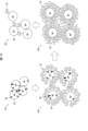
- FIG. 8 a process for heat-treating the plurality of nickel oxide nanoparticles in an oxygen atmosphere after the process for providing the coating portion, and a process for removing the coating portion.
- 10A to 10C are diagrams showing the schematic state of nickel oxide nanoparticles in each step shown in FIG. 9 .
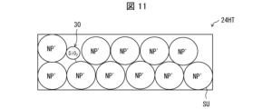
- 3 is a cross-sectional view showing a schematic configuration of a hole transport layer, which is a charge transport layer, provided in each of a red light-emitting element, a green light-emitting element, and a blue light-emitting element provided in the display device of embodiment 1.
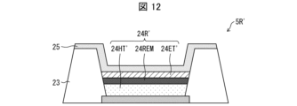
- FIG. 11 is a cross-sectional view showing a schematic configuration of a red light emitting element provided in a display device of embodiment 2.
- FIG. 13 is a cross-sectional view showing a schematic configuration of an electron transport layer, which is a charge transport layer provided in the red light emitting element shown in FIG. 12.
- 11 is a cross-sectional view showing a schematic configuration of a red light emitting element provided in a display device of embodiment 3.
- FIG. 13 is a cross-sectional view showing a schematic configuration of an electron transport layer, which is a charge transport layer provided in the red light emitting element shown in FIG. 12.
- 11 is a cross-sectional view showing a schematic configuration of a red light emitting element provided in a display device of embodiment 3.
- FIG. 1 is a plan view showing a schematic configuration of a display device 1 according to the first embodiment.
- the display device 1 has a frame area NDA and a display area DA.
- the display area DA of the display device 1 has a plurality of pixels PIX, each of which includes a red subpixel RSP, a green subpixel GSP, and a blue subpixel BSP.
- a case in which one pixel PIX is composed of a red subpixel RSP, a green subpixel GSP, and a blue subpixel BSP will be described as an example, but this is not limiting.
- one pixel PIX may include subpixels of other colors in addition to the red subpixel RSP, green subpixel GSP, and blue subpixel BSP.
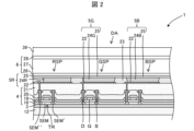
- FIG. 2 is a cross-sectional view showing the schematic configuration of the display area DA of the display device 1 of the first embodiment.
- a barrier layer 3 As shown in FIG. 2, in the display area DA of the display device 1, a barrier layer 3, a thin-film transistor layer 4 including a transistor TR, a red light-emitting element 5R, a green light-emitting element 5G, a blue light-emitting element 5B, a bank 23, a sealing layer 6, and a functional film 39 are provided on a substrate 12 in this order from the substrate 12 side.
- the red sub-pixel RSP provided in the display area DA of the display device 1 includes a red light-emitting element 5R as a light-emitting element
- the green sub-pixel GSP provided in the display area DA of the display device 1 includes a green light-emitting element 5G as a light-emitting element
- the blue sub-pixel BSP provided in the display area DA of the display device 1 includes a blue light-emitting element 5B as a light-emitting element.
- the substrate 12 may be, for example, a resin substrate made of a resin material such as polyimide, or a glass substrate.
- the substrate 12 in order to make the display device 1 a flexible display device, is made of, for example, a resin substrate made of a resin material such as polyimide, but this is not limited to this. If the display device 1 is a non-flexible display device, the substrate 12 may be made of, for example, a glass substrate.
- the barrier layer 3 is a layer that prevents foreign substances such as water and oxygen from penetrating the transistor TR, the red light-emitting element 5R, the green light-emitting element 5G, and the blue light-emitting element 5B, and can be composed of, for example, a silicon oxide film, a silicon nitride film, or a silicon oxynitride film, or a laminate film of these, formed by the CVD method.
- the transistor TR portion of the thin-film transistor layer 4 including the transistor TR includes the semiconductor film SEM and doped semiconductor films SEM' and SEM'', the inorganic insulating film 16, the gate electrode G, the inorganic insulating film 18, the inorganic insulating film 20, the source electrode S and the drain electrode D, and the planarization film 21, and the portion of the thin-film transistor layer 4 including the transistor TR other than the transistor TR portion includes the inorganic insulating film 16, the inorganic insulating film 18, the inorganic insulating film 20, and the planarization film 21.
- the semiconductor films SEM, SEM', and SEM'' may be made of, for example, low-temperature polysilicon (LTPS) or an oxide semiconductor (for example, an In-Ga-Zn-O-based semiconductor).
- LTPS low-temperature polysilicon
- oxide semiconductor for example, an In-Ga-Zn-O-based semiconductor.
- the gate electrode G and the source and drain electrodes S and D can be formed of a single layer or a multilayer film of a metal containing at least one of aluminum, tungsten, molybdenum, tantalum, chromium, titanium, and copper, for example.
- Inorganic insulating film 16, inorganic insulating film 18, and inorganic insulating film 20 can be composed of, for example, a silicon oxide film, a silicon nitride film, a silicon oxynitride film, or a laminate film of these films formed by the CVD method.
- the planarization film 21 can be made of a coatable organic material such as polyimide or acrylic.
- the red light-emitting element 5R included in the red subpixel RSP includes an anode 22 above the planarization film 21, a functional layer 24R including a red light-emitting layer, and a cathode 25.
- the green light-emitting element 5G included in the green subpixel GSP includes an anode 22 above the planarization film 21, a functional layer 24G including a green light-emitting layer, and a cathode 25.
- the blue light-emitting element 5B included in the blue subpixel BSP includes an anode 22 above the planarization film 21, a functional layer 24B including a blue light-emitting layer, and a cathode 25.
- the insulating bank 23 covering the edge of the anode 22 can be formed by applying an organic material such as polyimide or acrylic and then patterning it by photolithography.
- the functional layer 24R including the red light-emitting layer is configured by stacking a hole transport layer, a red light-emitting layer, and an electron transport layer in this order from the anode 22 side, but is not limited to this.
- the functional layer 24R including the red light-emitting layer may be configured by stacking, for example, a hole injection layer, a hole transport layer, a red light-emitting layer, an electron transport layer, and an electron injection layer in this order from the anode 22 side, or may be configured to include a red light-emitting layer and one or more layers selected from the group consisting of a hole injection layer, a hole transport layer, an electron transport layer, and an electron injection layer, which are charge transport layers.
- the functional layer 24G including the green light-emitting layer is configured by stacking a hole transport layer, a green light-emitting layer, and an electron transport layer in this order from the anode 22 side, but is not limited to this.
- the functional layer 24G including the green light-emitting layer may be configured by stacking, for example, a hole injection layer, a hole transport layer, a green light-emitting layer, an electron transport layer, and an electron injection layer in this order from the anode 22 side, and may be configured to include, for example, a green light-emitting layer and one or more layers selected from the group consisting of a hole injection layer, a hole transport layer, an electron transport layer, and an electron injection layer, which are charge transport layers.
- the functional layer 24B including the blue light-emitting layer is configured by stacking a hole transport layer, a blue light-emitting layer, and an electron transport layer in this order from the anode 22 side, but is not limited to this.
- the functional layer 24B including the blue light-emitting layer may be configured by stacking, for example, a hole injection layer, a hole transport layer, a blue light-emitting layer, an electron transport layer, and an electron injection layer in this order from the anode 22 side, or may be configured to include a blue light-emitting layer and one or more of the charge transport layers of the hole injection layer, hole transport layer, electron transport layer, and electron injection layer.
- the functional layer 24R including the red light-emitting layer, the functional layer 24G including the green light-emitting layer, and the functional layer 24B including the blue light-emitting layer each include a hole transport layer formed in the same process using the same material, and an electron transport layer formed in the same process using the same material, but the present invention is not limited to this.
- the hole transport layers included in each of the functional layers 24R, 24G, and 24B may be formed from different materials.
- the hole transport layers included in two of the functional layers 24R, 24G, and 24B may be formed in the same process using the same material, and only the hole transport layer included in the remaining functional layer may be formed in a separate process using a different material.
- the electron transport layers included in each of the functional layers 24R, 24G, and 24B may be formed from different materials.
- the electron transport layers included in two of the functional layers 24R, 24G, and 24B may be formed in the same process using the same material, and only the electron transport layer included in the remaining functional layer may be formed in a separate process using a different material.
- the red light-emitting element 5R, green light-emitting element 5G, and blue light-emitting element 5B are each a QLED (quantum dot light-emitting diode) having a light-emitting layer containing quantum dots.
- QLED quantum dot light-emitting diode
- each of the red light-emitting element 5R, green light-emitting element 5G, and blue light-emitting element 5B may be an OLED (organic light-emitting diode) having an organic light-emitting layer.
- red light-emitting element 5R, green light-emitting element 5G, and blue light-emitting element 5B may be QLEDs, and the remaining parts of the red light-emitting element 5R, green light-emitting element 5G, and blue light-emitting element 5B may be OLEDs.
- a control circuit including a transistor TR that controls the red light-emitting element 5R, a control circuit including a transistor TR that controls the green light-emitting element 5G, and a control circuit including a transistor TR that controls the blue light-emitting element 5B are provided in the thin-film transistor layer 4 including transistors TR for each of the red sub-pixels RSP, green sub-pixels GSP, and blue sub-pixels BSP.
- the control circuits including transistors TR and the light-emitting elements provided for each of the red sub-pixels RSP, green sub-pixels GSP, and blue sub-pixels BSP are collectively referred to as sub-pixel circuits.
- the red light-emitting element 5R, green light-emitting element 5G, and blue light-emitting element 5B shown in FIG. 2 may be of a top emission type or a bottom emission type.
- the red light-emitting element 5R, green light-emitting element 5G, and blue light-emitting element 5B have a stack structure in which the anode 22, the functional layers 24R, 24G, and 24B, and the cathode 25 are formed in this order from the substrate 12 side, and the cathode 25 is disposed as an upper layer than the anode 22.
- the anode 22 may be formed of an electrode material that reflects visible light
- the cathode 25 may be formed of an electrode material that transmits visible light
- the anode 22 may be formed of an electrode material that transmits visible light
- the cathode 25 may be formed of an electrode material that reflects visible light.
- the red light-emitting element 5R, the green light-emitting element 5G, and the blue light-emitting element 5B may have an inverted stack structure in which, from the substrate 12 side, the cathode 25, each functional layer (for example, from the substrate 12 side, the electron transport layer, the light-emitting layer, and the hole transport layer are stacked in this order), and the anode 22 are formed in this order.
- the anode 22 is disposed as an upper layer than the cathode 25. Therefore, in order to form a top emission type, the cathode 25 may be formed from an electrode material that reflects visible light, and the anode 22 may be formed from an electrode material that transmits visible light. In order to form a bottom emission type, the cathode 25 may be formed from an electrode material that transmits visible light, and the anode 22 may be formed from an electrode material that reflects visible light.
- the electrode material that reflects visible light is not particularly limited as long as it can reflect visible light and has electrical conductivity, but examples include metal materials such as Al, Mg, Li, and Ag, alloys of the above metal materials, laminates of the above metal materials and transparent metal oxides (e.g., indium tin oxide, indium zinc oxide, indium gallium zinc oxide, etc.), and laminates of the above alloys and the above transparent metal oxides.
- metal materials such as Al, Mg, Li, and Ag
- alloys of the above metal materials such as Al, Mg, Li, and Ag
- alloys of the above metal materials such as Al, Mg, Li, and Ag
- laminates of the above metal materials and transparent metal oxides e.g., indium tin oxide, indium zinc oxide, indium gallium zinc oxide, etc.
- laminates of the above alloys and the above transparent metal oxides e.g., indium tin oxide, indium zinc oxide, indium gallium zinc oxide, etc.
- electrode materials that transmit visible light are not particularly limited as long as they are capable of transmitting visible light and have electrical conductivity, but examples include transparent metal oxides (e.g., indium tin oxide, indium zinc oxide, indium gallium zinc oxide, etc.), thin films made of metal materials such as Al and Ag, and nanowires made of metal materials such as Al and Ag.
- transparent metal oxides e.g., indium tin oxide, indium zinc oxide, indium gallium zinc oxide, etc.
- thin films made of metal materials such as Al and Ag
- nanowires made of metal materials such as Al and Ag.
- the red light-emitting element 5R, the green light-emitting element 5G, and the blue light-emitting element 5B are top-emission types with a forward stack structure, so the anode 22 is formed from a laminated film of ITO (indium tin oxide)/Ag/ITO, which is an electrode material that reflects visible light, and the cathode 25 is formed from a thin film of Ag, which is an electrode material that transmits visible light, but the present invention is not limited to this example.
- the sealing layer 6 is a light-transmitting film, and can be composed of, for example, an inorganic sealing film 26 that covers the cathode 25, an organic film 27 that is above the inorganic sealing film 26, and an inorganic sealing film 28 that is above the organic film 27.
- the sealing layer 6 prevents foreign matter such as water and oxygen from penetrating into the red light-emitting element 5R, the green light-emitting element 5G, and the blue light-emitting element 5B.
- the inorganic sealing film 26 and the inorganic sealing film 28 are inorganic films, and may be formed, for example, by a CVD method, such as a silicon oxide film, a silicon nitride film, or a silicon oxynitride film, or a laminated film of these.
- the organic film 27 is a light-transmitting organic film with a planarizing effect, and may be formed, for example, by a coatable organic material such as acrylic.
- the organic film 27 may be formed, for example, by an inkjet method.
- the sealing layer 6 is formed of two inorganic films and one organic film provided between the two inorganic films, but the lamination order of the two inorganic films and one organic film is not limited to this.
- the sealing layer 6 may be formed only of an inorganic film, may be formed only of an organic film, may be formed of one inorganic film and two organic films, or may be formed of two or more inorganic films and two or more organic films.
- the functional film 39 is, for example, a film having at least one of an optical compensation function, a touch sensor function, and a protective function.
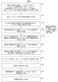
- FIG. 3 is a diagram showing the manufacturing process of the display device 1 of embodiment 1, including the manufacturing process of the red light-emitting element 5R, the green light-emitting element 5G, and the blue light-emitting element 5B.
- the manufacturing process of the display device 1 shown in FIG. 2 equipped with the light-emitting element of the forward stack structure includes the steps of forming a barrier layer 3 and a thin-film transistor layer 4 on a substrate 12 (S1), forming an anode 22 (S2), forming a bank 23 (S3), forming a functional layer 24R including a red light-emitting layer included in the red light-emitting element 5R, a functional layer 24G including a green light-emitting layer included in the green light-emitting element 5G, and a functional layer 24B including a blue light-emitting layer included in the blue light-emitting element 5B (S4), forming a cathode 25 (S5), forming a sealing layer 6 (S6), and forming a functional film 39 (S7).
- the manufacturing process of the display device equipped with the light-emitting element of the reverse stack structure is the same as the manufacturing process of the display device 1 equipped with the light-emitting element of the forward stack structure shown in FIG. 3, except that the order of the step (S2) of forming the anode 22 and the step (S5) of forming the cathode 25 is reversed.
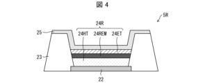
- FIG. 4 is a cross-sectional view showing the schematic configuration of a red light-emitting element 5R provided in the display device 1 of embodiment 1.
- FIG. 5 is a cross-sectional view showing the schematic configuration of a green light-emitting element 5G provided in the display device 1 of embodiment 1.
- FIG. 6 is a cross-sectional view showing the schematic configuration of blue light-emitting element 5B provided in display device 1 of embodiment 1.
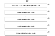
- FIG. 7 is a diagram showing the process of forming the functional layers 24R, 24G, and 24B in the manufacturing process of the display device 1 of embodiment 1 shown in FIG. 3.
- the process of forming the functional layer 24R in the red light-emitting element 5R, the functional layer 24G in the green light-emitting element 5G, and the functional layer 24B in the blue light-emitting element 5B includes a step of forming a hole transport layer 24HT on the anode 22 (S11), a step of forming a light-emitting layer 24REM (red light-emitting layer) (S12), a step of forming a light-emitting layer 24GEM (green light-emitting layer) (S13), a step of forming a light-emitting layer 24BEM (blue light-emitting layer) (S14), and a step of forming an electron transport layer 24ET (S15).
- the light-emitting layer 24REM red light-emitting layer
- the light-emitting layer 24GEM green light-emitting layer
- the light-emitting layer 24BEM blue light-emitting layer
- each of the functional layers 24R, 24G, and 24B includes a hole transport layer 24HT formed in the same process using the same material, so that in the process (S11) of forming the hole transport layer 24HT on the anode 22, as shown in Figures 4, 5, and 6, a hole transport layer 24HT is formed on the anode 22 provided on each of the red light-emitting element 5R, green light-emitting element 5G, and blue light-emitting element 5B.
- each of the functional layers 24R, 24G, and 24B includes an electron transport layer 24ET formed in the same process using the same material, so in the process (S15) of forming the electron transport layer 24ET, as shown in Figures 4, 5, and 6, the electron transport layer 24ET is formed on the light-emitting layer 24REM (red light-emitting layer) provided in the red light-emitting element 5R, the light-emitting layer 24GEM (green light-emitting layer) provided in the green light-emitting element 5G, and the light-emitting layer 24BEM (blue light-emitting layer) provided in the blue light-emitting element 5B.
- the light-emitting layer 24REM red light-emitting layer
- the light-emitting layer 24GEM green light-emitting layer
- the light-emitting layer 24BEM blue light-emitting layer
- the anode 22 can be formed with a thickness of, for example, 100 nm or more and 300 nm or less, but is not limited to this.
- the cathode 25 can be formed with a thickness of, for example, 10 nm or more and 100 nm or less, but is not limited to this.
- the hole transport layer 24HT can be formed with a thickness of, for example, 10 nm or more and 150 nm or less, but is not limited to this.
- the light-emitting layer 24REM red light-emitting layer
- the light-emitting layer 24GEM green light-emitting layer
- the light-emitting layer 24BEM blue light-emitting layer
- the electron transport layer 24ET can be formed with a thickness of, for example, 30 nm or more and 120 nm or less, but is not limited to this.
- the electron transport layer 24ET can be formed, for example, using zinc oxide nanoparticles having surface oxygen defects DE.
- nickel oxide nanoparticles are used as an example of metal oxide nanoparticles used in the step (S11) of forming the hole transport layer 24HT on the anode 22, but there is no particular limitation as long as the metal oxide nanoparticles are hole transport materials used in the step of forming at least one of the hole transport layer 24HT and the hole injection layer provided between the anode 22 and the light emitting layers 24REM, 24GEM, and 24BEM.
- the metal oxide nanoparticles as hole transport materials may be metal oxide nanoparticles containing at least one of Ni, Mg, Mo, Cu, Co, Cr, and Ti.
- the metal oxide nanoparticles may be metal oxide nanoparticles that are electron transport materials used in the process of forming at least one of the electron transport layer 24ET' and the electron injection layer provided between the cathode 25 and the light-emitting layer 24REM.
- the metal oxide nanoparticles that are electron transport materials may be metal oxide nanoparticles that contain at least one of Zn, Mg, Ti, Si, Sn, W, Ta, Ba, Zr, Al, Y, and Hf.
- the metal oxide nanoparticles that are electron transport materials may be zinc oxide or zinc magnesium oxide nanoparticles.
- the particle size of the metal oxide nanoparticles is not particularly limited, but is preferably, for example, 1 nm or more and 1000 nm or less.
- the particle size of the metal oxide nanoparticles is 1 nm or more, it becomes easy to control the particle size of the metal oxide nanoparticles.
- the particle size of the metal oxide nanoparticles is 1000 nm or less, it is possible to improve the efficiency of injection of holes from the anode 22 or injection of electrons from the cathode 25.
- Figure 8 shows the manufacturing process for nickel oxide nanoparticles NP, which are metal oxide nanoparticles having surface oxygen defects DE.
- the manufacturing process for nickel oxide nanoparticles NP which are metal oxide nanoparticles having surface oxygen defects DE, includes a step (S21) of preparing an aqueous solution containing nickel element, a step (S22) of adding an alkaline solution, a stirring step (S23), a drying step (S24), a heat treatment step (S25), and a filtering step (S26).
- step (S21) of preparing an aqueous solution containing nickel for example, 7.27 g of Ni(NO 3 ) 2.6H 2 O is dispersed in 10 ml of pure water to prepare an aqueous solution containing nickel.
- step (S22) of adding an alkaline solution for example, 5.85 to 5.9 ml of a 10N (N is normality) NaOH aqueous solution is added.
- the NaOH aqueous solution may be added, for example, at a rate of 0.3 to 0.4 ml/min while stirring, until the pH becomes about 10.
- the stirring step (S23) the solution is stirred for, for example, about 5 minutes.
- nickel oxide nanoparticles can be obtained in an alkaline environment by the chemical precipitation method.
- a washing step of washing the nickel oxide nanoparticles may be performed.
- a heat treatment is performed, for example, at 80° C. for 15 to 24 hours to dry the nickel oxide nanoparticles.
- a pulverization step may be performed to pulverize the nickel oxide nanoparticles.
- heat treatment step (S25) for example, heat treatment is performed in the presence of oxygen at 250°C to 270°C for 2 hours to 4 hours to calcine the nickel oxide nanoparticles.
- the filter treatment step (S26) the calcined nickel oxide nanoparticles are pulverized, and the pulverized nickel oxide nanoparticles are put into pure water and stirred to disperse, and then passed through, for example, a PTFE filter with a pore size of 1 ⁇ m to obtain nickel oxide nanoparticles with a particle size of 1000 nm or less.
- surface oxygen defects DE are generated on the surface SU of the nickel oxide nanoparticle NP due to a lack of intermolecular interactions.
- Surface oxygen defects DE refer to oxygen defects formed on the surface due to a lack of intermolecular interactions on the surface of the metal oxide nanoparticle.
- the nickel oxide nanoparticles NP manufactured by the manufacturing process of nickel oxide nanoparticles NP shown in Figure 8 have been described as an example, but the present invention is not limited to this, and it is known that such surface oxygen defects DE occur in the case of nickel oxide nanoparticles manufactured by commonly known manufacturing processes of nickel oxide nanoparticles. Furthermore, the present invention is not limited to nickel oxide nanoparticles, and it is known that such surface oxygen defects DE occur in the case of metal oxide nanoparticles (e.g., zinc oxide or magnesium zinc oxide nanoparticles, etc.).
- metal oxide nanoparticles e.g., zinc oxide or magnesium zinc oxide nanoparticles, etc.
- FIG. 9 is a diagram for explaining the steps (S31 to S39) of providing a coating portion 30 containing an inorganic oxide on the surface SU of each of the nickel oxide nanoparticles NP produced by the nickel oxide nanoparticle NP production process shown in FIG. 8, the step (S40) of heat-treating the nickel oxide nanoparticles NP in an oxygen atmosphere after the step of providing the coating portion 30, and the step (S41) of removing the coating portion 30.
- FIG. 10 shows the general state of nickel oxide nanoparticles NP and NP' at each step shown in FIG. 9.
- FIG. 11 is a cross-sectional view showing a schematic configuration of the hole transport layer 24HT, which is a charge transport layer provided in each of the red light-emitting element 5R, the green light-emitting element 5G, and the blue light-emitting element 5B provided in the display device 1 of embodiment 1.
- the hole transport layer 24HT is a charge transport layer provided in each of the red light-emitting element 5R, the green light-emitting element 5G, and the blue light-emitting element 5B provided in the display device 1 of embodiment 1.
- nickel oxide nanoparticles NP' which are multiple metal oxide nanoparticles, that is, nickel oxide nanoparticles NP having surface oxygen vacancies DE on their surface SU, are produced by a method for producing nickel oxide nanoparticles NP', which includes steps (S31 to S39) of providing a coating portion 30 containing an inorganic oxide on the surface SU of the nickel oxide nanoparticles NP, and a step (S40) of heat-treating the nickel oxide nanoparticles NP in an oxygen atmosphere after the step of providing the coating portion 30.
- steps (S31 to S39) of providing a coating portion 30 containing an inorganic oxide on the surface SU of the nickel oxide nanoparticles NP and a step (S40) of heat-treating the nickel oxide nanoparticles NP in an oxygen atmosphere after the step of providing the coating portion 30.
- nickel oxide nanoparticles NP' which are metal oxide nanoparticles that are highly reliable because they have a coating portion 30 made of an inorganic oxide, and that have no surface oxygen defects DE, thereby suppressing the decrease in luminous efficiency associated with a decrease in external quantum efficiency (EQE).
- the above-mentioned method for producing nickel oxide nanoparticles NP' preferably includes a step (S41) of removing the coating portion 30 after the heat treatment step (S40).
- the degree of change in the energy level of the metal oxide nanoparticles due to the effect of surface oxygen defects DE, which are formed in random numbers at random positions on the surface of the metal oxide nanoparticles is small. Therefore, in the step (S41) of removing the coating portion 30, the coating portion 30 made of an inorganic oxide may be removed, but a part of the coating portion 30 made of an inorganic oxide that plays a role in suppressing the aggregation of the nickel oxide nanoparticles NP' may be left. Alternatively, the step (S41) of removing the coating portion 30 may be omitted, and the entire coating portion 30 made of an inorganic oxide may be left.
- the manufacturing method of the light-emitting elements includes a step of forming a hole transport layer 24HT, which is a charge transport layer.
- the step of forming the hole transport layer 24HT includes a step of providing a coating portion 30 containing an inorganic oxide (S31 to S39) and, after the step of providing the coating portion 30, a step of heat-treating nickel oxide nanoparticles NP in an oxygen atmosphere (S40).
- the above-mentioned process for forming the hole transport layer 24HT preferably includes a process (S41) for removing the covering portion 30 after the heat treatment process (S40).
- the steps of providing the coating portion 30 containing an inorganic oxide include the steps of preparing a nickel oxide nanoparticle dispersion solution (S31, first step), stirring the nickel oxide nanoparticle dispersion solution (S32), adding a catalyst solution containing water and a catalyst for hydrolysis reaction (S33), stirring the nickel oxide nanoparticle dispersion solution to which the catalyst solution has been added (S34), adding a precursor solution containing an alcohol solvent and a precursor of the inorganic oxide that constitutes the coating portion 30 (S35), stirring the nickel oxide nanoparticle dispersion solution containing the catalyst and precursor (S36), centrifuging the nickel oxide nanoparticle dispersion solution containing the catalyst and precursor to remove the solvent (S37, fourth step), washing with alcohol (S38, fifth step), and drying (S39, third step).
- step (S31) of preparing a nickel oxide nanoparticle dispersion solution for example, nickel oxide nanoparticles NP having surface oxygen defects DE on their surface SU are put into 1 L of ethanol, which is an alcohol solvent containing 10 g of N-vinyl-2-pyrrolidone as a dispersant.
- step (S32) of stirring the nickel oxide nanoparticle dispersion solution the nickel oxide nanoparticle dispersion solution is stirred for, for example, 12 hours.
- step (S33) of adding a catalyst solution containing water and a catalyst for hydrolysis reaction for example, 100 ml of water and a 25% ammonia solution containing 25 wt % NH 3 per 100 ml of water are added.
- a case where a base catalyst is used as a catalyst for hydrolysis reaction is described as an example, but an acid catalyst may be used as the catalyst for hydrolysis reaction.
- stirring is performed for 30 minutes using, for example, ultrasonic waves.
- TEOS tetraethoxysilane
- TEOS tetraethoxysilane
- M is a metal element or a metalloid element other than Si, and R is an alkyl group.
- steps S33 to S35 are the second step of preparing a nickel oxide nanoparticle dispersion solution (sol) containing a catalyst and a precursor.
- step (S36) of stirring the nickel oxide nanoparticle dispersion solution containing the catalyst and precursor stirring was performed using ultrasonic waves for 1 hour and 30 minutes.
- step (S37) of centrifuging the nickel oxide nanoparticle dispersion solution containing the catalyst and precursor to remove the solvent a centrifuge was used to remove the solvent, ethanol.
- step (S38) of washing with alcohol for example, washing was performed one or more times using ethanol.
- step (S39) of drying drying was performed, for example, by heat treatment at 70°C for 5 hours.
- stirring may be performed using, for example, a stirrer, or ultrasonic waves may be used.
- the process (S31 to S39) of providing the coating portion 30 containing an inorganic oxide includes a total of three stirring steps, but this is not limited to this, and the number of stirring steps may be more than three or less than three, and no stirring step may be included.
- the step (S33) of adding a catalyst solution containing water and a catalyst for hydrolysis reaction and the step (S35) of adding a precursor solution containing an alcohol solvent and a precursor of an inorganic oxide that constitutes the coating portion 30 are performed in this order as an example, but this is not limited to this, and the step (S35) of adding a precursor solution containing an alcohol solvent and a precursor of an inorganic oxide that constitutes the coating portion 30 may be performed first, and then the step (S33) of adding a catalyst solution containing water and a catalyst for hydrolysis reaction may be performed.
- the process (S31 to S39) of providing the coating portion 30 containing an inorganic oxide is described as including both the process (S37) of centrifuging the nickel oxide nanoparticle dispersion solution containing the catalyst and precursor to remove the solvent and the process (S38) of washing with alcohol, but this is not limited thereto, and at least one of the process (S37) of centrifuging the nickel oxide nanoparticle dispersion solution containing the catalyst and precursor to remove the solvent and the process (S38) of washing with alcohol may be omitted.
- an alcohol solvent e.g., ethanol
- TEOS tetraethoxysilane
- the steps (S31 to S39) of providing the coating portion 30 containing an inorganic oxide can gel tetraethoxysilane (TEOS), which is a precursor of the inorganic oxide that constitutes the coating portion 30.
- TEOS tetraethoxysilane
- the gelation of tetraethoxysilane (TEOS) also progresses in the step (S36) of stirring the nickel oxide nanoparticle dispersion solution containing the catalyst and precursor, but the gelation of tetraethoxysilane (TEOS) can be further promoted by removing the solvent in the step (S37) of centrifuging the nickel oxide nanoparticle dispersion solution containing the catalyst and precursor to remove the solvent and the drying step (S39).
- the coating portion 30 after the drying step (S39) is composed of a porous inorganic oxide containing an organic group, which includes a portion containing an O-Si-O bond, which is an inorganic oxide, and a portion containing a residual ethoxy group (OCH 2 CH 3 ) bonded to Si and a residual OH group (not shown).
- the coating portion 30 made of a porous inorganic oxide containing organic groups can suppress the aggregation of nickel oxide nanoparticles NP having surface oxygen vacancies DE, and increase the distance between the nickel oxide nanoparticles NP.
- a process (S40) is performed in which nickel oxide nanoparticles NP, which are metal oxide nanoparticles, are heat-treated in an oxygen atmosphere while the nickel oxide nanoparticles NP having surface oxygen vacancies DE are spaced apart by a coating portion 30 made of a porous inorganic oxide containing organic groups.
- the heat treatment is performed while supplying oxygen O2 at a predetermined flow rate as shown in FIG. 10, but this is not limited thereto, and for example, the heat treatment may be performed in the air, which is an oxygen atmosphere.
- the composition ratio of nickel element to oxygen element contained in the nickel oxide nanoparticles NP′ can be made 1:1 by appropriately adjusting the flow rate.
- the step (S40) of heat treating the nickel oxide nanoparticles NP, which are multiple metal oxide nanoparticles, in an oxygen atmosphere is preferably carried out at a temperature of 500°C or higher for 3 hours or more.
- the covering portion 30 can be made of silicon oxide, which is an inorganic oxide, and reliability can be improved even when at least a portion of the covering portion 30 is left unremoved.
- the nickel oxide nanoparticles NP' which are a plurality of metal oxide nanoparticles, are washed with an alkaline solution to remove the coating portions 30.
- an alkaline solution for example, an aqueous NaOH solution can be used, and the number of remaining coating portions 30 can be appropriately adjusted by appropriately controlling the concentration of the alkaline solution, the number of times washing with the alkaline solution, and the time that the nickel oxide nanoparticles NP' are in contact with the alkaline solution.
- the hole transport layer 24HT which is a charge transport layer provided in each of the red light emitting element 5R, the green light emitting element 5G, and the blue light emitting element 5B provided in the display device 1 of embodiment 1, some of the nickel oxide nanoparticles NP' among the multiple nickel oxide nanoparticles NP' may be provided with a covering portion 30 on at least a portion of their surface SU.
- FIG. 11 is a cross-sectional view of a predetermined size of the hole transport layer 24HT, where the total number of nickel oxide nanoparticles NP' included in the cross-section of the predetermined size is A, and the number of nickel oxide nanoparticles NP' provided with a coating portion 30 included in the cross-section of the predetermined size is B, it is preferable that (B/A) is 0.1 or less. In FIG. 11, A is 11, B is 1, and (B/A) is 0.09.
- nickel oxide nanoparticle NP' even when a portion of a nickel oxide nanoparticle NP' is included in the cross-section of the predetermined size, it is counted as one, and when only a coating portion 30 is included in the cross-section of the predetermined size, it is counted as a nickel oxide nanoparticle NP' provided with a coating portion 30.
- the red light emitting element 5R, the green light emitting element 5G, and the blue light emitting element 5B, which are provided with the hole transport layer 24HT shown in FIG. 11, and the display device 1, which is provided with the red light emitting element 5R, the green light emitting element 5G, and the blue light emitting element 5B, are highly reliable and can suppress the decrease in luminous efficiency associated with the decrease in external quantum efficiency (EQE).
- the red light emitting element 5R' of this embodiment differs from the first embodiment described above in that it includes an electron transport layer 24ET' containing zinc oxide nanoparticles NP1', which are a plurality of metal oxide nanoparticles that do not have surface oxygen defects DE.
- the rest is as described in the first embodiment.
- members having the same functions as the members shown in the drawings of the first embodiment are given the same reference numerals, and their explanation will be omitted.
- FIG. 12 is a cross-sectional view showing the schematic configuration of a red light-emitting element 5R' provided in the display device of embodiment 2.
- FIG. 13 is a cross-sectional view showing the schematic configuration of the electron transport layer 24ET', which is a charge transport layer provided in the red light-emitting element 5R' shown in FIG. 12.
- the red light emitting element 5R' shown in FIG. 12 includes an electron transport layer 24ET' including zinc oxide nanoparticles NP1', which are a plurality of metal oxide nanoparticles having no surface oxygen defect DE, as shown in FIG. 13.
- the flow rate can be appropriately adjusted to make the composition ratio of the metal element (zinc element) and the oxygen element contained in the zinc oxide nanoparticles NP1' 1:1.
- the case where the zinc oxide nanoparticles NP1' are used is described as an example, but the present invention is not limited to this, and for example, magnesium zinc oxide nanoparticles may be used.
- the electron transport layer 24ET' can be formed to a thickness of, for example, 30 nm or more and 120 nm or less, but is not limited thereto.
- the hole transport layer 24HT' provided in the red light emitting element 5R' shown in FIG. 12 can be formed, for example, using nickel oxide nanoparticles NP having surface oxygen defects DE.
- the hole transport layer 24HT' can be formed to a thickness of, for example, 10 nm or more and 150 nm or less, but is not limited to this.
- some of the zinc oxide nanoparticles NP1' among the plurality of zinc oxide nanoparticles NP1' may be provided with a covering portion 30 on at least a portion of their surface SU.
- FIG. 13 is a cross-sectional view of a predetermined size of the electron transport layer 24ET', where the total number of zinc oxide nanoparticles NP1' included in the cross-section of the predetermined size is A, and the number of zinc oxide nanoparticles NP1' provided with a coating portion 30 included in the cross-section of the predetermined size is B, it is preferable that (B/A) is 0.1 or less. In FIG. 13, A is 11, B is 1, and (B/A) is 0.09.
- the red light emitting element 5R' having the electron transport layer 24ET' shown in FIG. 13 and the display device of embodiment 2 having the red light emitting element 5R' are highly reliable and can suppress the decrease in luminous efficiency associated with the decrease in external quantum efficiency (EQE).
- the red light emitting element 5R′′ of this embodiment is different from the first and second embodiments described above in that it includes a hole transport layer 24HT including nickel oxide nanoparticles NP′, which are a plurality of metal oxide nanoparticles having no surface oxygen defect portions DE, and an electron transport layer 24ET′ including zinc oxide nanoparticles NP1′, which are a plurality of metal oxide nanoparticles having no surface oxygen defect portions DE.
- the rest is as described in the first and second embodiments.
- members having the same functions as those shown in the drawings of the first and second embodiments are denoted by the same reference numerals, and description thereof will be omitted.
- FIG. 14 is a cross-sectional view showing the schematic configuration of a red light-emitting element 5R'' provided in the display device of embodiment 3.
- the red light emitting element 5R'' includes a hole transport layer 24HT, which is a charge transport layer (first charge transport layer) containing nickel oxide nanoparticles NP', which are a plurality of metal oxide nanoparticles that do not have surface oxygen defects DE, and an electron transport layer 24ET', which is a charge transport layer (second charge transport layer) containing zinc oxide nanoparticles NP1', which are a plurality of second metal oxide nanoparticles that do not have surface oxygen defects DE.
- a hole transport layer 24HT which is a charge transport layer (first charge transport layer) containing nickel oxide nanoparticles NP', which are a plurality of metal oxide nanoparticles that do not have surface oxygen defects DE
- an electron transport layer 24ET' which is a charge transport layer (second charge transport layer) containing zinc oxide nanoparticles NP1', which are a plurality of second metal oxide nanoparticles that do not have surface oxygen defects DE.
- the red light emitting element 5R'' having the hole transport layer 24HT and the electron transport layer 24ET' shown in FIG. 14 and the display device of embodiment 3 having the red light emitting element 5R'' have higher reliability and can further suppress the decrease in luminous efficiency associated with the decrease in external quantum efficiency (EQE).
- the present invention can be used in light-emitting devices, display devices, methods for manufacturing light-emitting devices, and methods for manufacturing metal oxide nanoparticles.
Landscapes
- Engineering & Computer Science (AREA)
- Physics & Mathematics (AREA)
- Optics & Photonics (AREA)
- Manufacturing & Machinery (AREA)
- Chemical & Material Sciences (AREA)
- Crystallography & Structural Chemistry (AREA)
- Inorganic Chemistry (AREA)
- Nanotechnology (AREA)
- Electroluminescent Light Sources (AREA)
Abstract
発光素子は、電荷輸送層として正孔輸送層(24HT)を備えており、正孔輸送層(24HT)は、表面酸素欠陥部(DE)を有さない複数の酸化ニッケルのナノ粒子(NP')を含み、複数の酸化ニッケルのナノ粒子(NP')のうちの一つ以上の酸化ニッケルのナノ粒子(NP')は、その表面(SU)の少なくとも一部に、無機酸化物で構成される被覆部(30)が設けられている。
Description
本開示は、発光素子、表示装置、発光素子の製造方法及び金属酸化物ナノ粒子の製造方法に関する。
近年、発光素子を備えた様々な表示装置が開発されており、特に、OLED(Organic Light Emitting Diode:有機発光ダイオード)または、QLED(Quantum dot Light Emitting Diode:量子ドット発光ダイオード)を備えた表示装置は、低消費電力化、薄型化及び高画質化などを実現できる点から、高い注目を浴びている。
OLEDまたは、QLEDの分野においては、高い電荷輸送性(キャリア(正孔または電子)輸送性)を有することから、正孔輸送層、正孔注入層、電子輸送層及び電子注入層などの電荷輸送層として、有機材料が主に用いられていた。
しかしながら、このような有機材料で形成した正孔輸送層、正孔注入層、電子輸送層及び電子注入層などの電荷輸送層の場合、信頼性に問題があった。
そこで、OLEDまたは、QLEDの電荷輸送層として用いることができる無機材料に関する研究が活発に行われている。
特許文献1は、無機材料である、例えば、酸化ニッケルのナノ結晶(ナノ粒子)を電荷輸送層に用いることについて開示している。
一般的に、金属酸化物ナノ粒子は、その製造工程において、その表面のランダムな位置にランダムな数の表面酸素欠陥部(金属酸化物ナノ粒子の表面において分子間相互作用の欠落で、表面に形成される酸素の欠陥部)が形成され、この表面酸素欠陥部の影響によりエネルギー準位が変化してしまい、金属酸化物ナノ粒子毎にエネルギー準位にバラツキが生じてしまう。このように表面に表面酸素欠陥部が形成された金属酸化物ナノ粒子を用いて形成した電荷輸送層を備えた発光素子の場合、外部量子効率(EQE)の低下に伴う発光効率の低下が生じてしまうという問題があった。
特許文献1には、金属酸化物ナノ粒子である酸化ニッケルのナノ結晶(ナノ粒子)と、電子吸引基を備える有機分子とを含む電荷輸送層を備えた発光素子について記載されている。
しかしながら、特許文献1に記載の発光素子に備えられた電荷輸送層に含まれる酸化ニッケルのナノ結晶(ナノ粒子)には依然として表面酸素欠陥部が残るので、上述した発光効率の低下を抑制できず、さらに、電子吸引基を備える有機分子を用いているので、信頼性にも問題がある。
本開示の一態様は、前記の問題点に鑑みてなされたものであり、信頼性が高く、外部量子効率(EQE)の低下に伴う発光効率の低下を抑制できる、発光素子と、表示装置と、発光素子の製造方法と、金属酸化物ナノ粒子の製造方法とを提供することを目的とする。
本開示の発光素子は、前記の課題を解決するために、
アノードと、
カソードと、
前記アノードと前記カソードとの間に設けられた発光層と、
前記アノード及び前記カソードの一方と前記発光層との間に設けられた電荷輸送層と、を備え、
前記電荷輸送層は、表面酸素欠陥部を有さない複数の金属酸化物ナノ粒子を含み、
前記複数の金属酸化物ナノ粒子のうちの一つ以上の金属酸化物ナノ粒子は、その表面の少なくとも一部に、無機酸化物で構成される被覆部が設けられている。
アノードと、
カソードと、
前記アノードと前記カソードとの間に設けられた発光層と、
前記アノード及び前記カソードの一方と前記発光層との間に設けられた電荷輸送層と、を備え、
前記電荷輸送層は、表面酸素欠陥部を有さない複数の金属酸化物ナノ粒子を含み、
前記複数の金属酸化物ナノ粒子のうちの一つ以上の金属酸化物ナノ粒子は、その表面の少なくとも一部に、無機酸化物で構成される被覆部が設けられている。
本開示の表示装置は、前記の課題を解決するために、
前記発光素子を含む。
前記発光素子を含む。
本開示の発光素子の製造方法は、前記の課題を解決するために、
複数の金属酸化物ナノ粒子それぞれの表面に、無機酸化物を含む被覆部を設ける工程と、
前記被覆部を設ける工程の後に、酸素雰囲気下で、前記複数の金属酸化物ナノ粒子を熱処理する工程と、を含む電荷輸送層の形成工程を含む。
複数の金属酸化物ナノ粒子それぞれの表面に、無機酸化物を含む被覆部を設ける工程と、
前記被覆部を設ける工程の後に、酸素雰囲気下で、前記複数の金属酸化物ナノ粒子を熱処理する工程と、を含む電荷輸送層の形成工程を含む。
本開示の金属酸化物ナノ粒子の製造方法は、前記の課題を解決するために、
複数の金属酸化物ナノ粒子それぞれの表面に、無機酸化物を含む被覆部を設ける工程と、
前記被覆部を設ける工程の後に、酸素雰囲気下で、前記複数の金属酸化物ナノ粒子を熱処理する工程と、を含む。
複数の金属酸化物ナノ粒子それぞれの表面に、無機酸化物を含む被覆部を設ける工程と、
前記被覆部を設ける工程の後に、酸素雰囲気下で、前記複数の金属酸化物ナノ粒子を熱処理する工程と、を含む。
本開示の一態様は、信頼性を向上できるとともに、外部量子効率(EQE)の低下に伴う発光効率の低下を抑制できる、発光素子と、表示装置と、発光素子の製造方法と、金属酸化物ナノ粒子の製造方法とを提供できる。
本発明の実施の形態について、図1から図14に基づいて説明すれば、次の通りである。以下、説明の便宜上、特定の実施形態にて説明した構成と同一の機能を有する構成については、同一の符号を付記し、その説明を省略する場合がある。
〔実施形態1〕
図1は、実施形態1の表示装置1の概略的な構成を示す平面図である。
図1は、実施形態1の表示装置1の概略的な構成を示す平面図である。
図1に示すように、表示装置1は、額縁領域NDAと、表示領域DAとを備えている。表示装置1の表示領域DAには、複数の画素PIXが備えられており、各画素PIXは、それぞれ、赤色サブ画素RSPと、緑色サブ画素GSPと、青色サブ画素BSPとを含む。本実施形態においては、1画素PIXが、赤色サブ画素RSPと、緑色サブ画素GSPと、青色サブ画素BSPとで構成される場合を一例に挙げて説明するが、これに限定されることはない。例えば、1画素PIXは、赤色サブ画素RSP、緑色サブ画素GSP及び青色サブ画素BSPの他に、さらに他の色のサブ画素を含んでいてもよい。
図2は、実施形態1の表示装置1の表示領域DAの概略的な構成を示す断面図である。
図2に示すように、表示装置1の表示領域DAにおいては、基板12上に、バリア層3と、トランジスタTRを含む薄膜トランジスタ層4と、赤色発光素子5R、緑色発光素子5G、青色発光素子5B及びバンク23と、封止層6と、機能フィルム39とが、基板12側からこの順に備えられている。
表示装置1の表示領域DAに備えられた赤色サブ画素RSPは発光素子として赤色発光素子5Rを含み、表示装置1の表示領域DAに備えられた緑色サブ画素GSPは発光素子として緑色発光素子5Gを含み、表示装置1の表示領域DAに備えられた青色サブ画素BSPは発光素子として青色発光素子5Bを含む。
基板12は、例えば、ポリイミドなどの樹脂材料からなる樹脂基板であってもよく、ガラス基板であってもよい。本実施形態においては、表示装置1を可撓性表示装置とするため、基板12として、例えば、ポリイミドなどの樹脂材料からなる樹脂基板を用いた場合を一例に挙げて説明するが、これに限定されることはない。表示装置1を非可撓性表示装置とする場合には、基板12として、例えば、ガラス基板を用いることができる。
バリア層3は、水、酸素などの異物がトランジスタTR、赤色発光素子5R、緑色発光素子5G及び青色発光素子5Bに侵入することを防ぐ層であり、例えば、CVD法により形成される、酸化シリコン膜、窒化シリコン膜、あるいは酸窒化シリコン膜、またはこれらの積層膜で構成することができる。
トランジスタTRを含む薄膜トランジスタ層4のトランジスタTR部分は、半導体膜SEM及びドープされた半導体膜SEM’・SEM’’と、無機絶縁膜16と、ゲート電極Gと、無機絶縁膜18と、無機絶縁膜20と、ソース電極S及びドレイン電極Dと、平坦化膜21とを含み、トランジスタTRを含む薄膜トランジスタ層4のトランジスタTR部分以外の部分は、無機絶縁膜16と、無機絶縁膜18と、無機絶縁膜20と、平坦化膜21とを含む。
半導体膜SEM・SEM’・SEM’’は、例えば、低温ポリシリコン(LTPS)あるいは酸化物半導体(例えば、In-Ga-Zn-O系の半導体)で構成してもよい。本実施形態においては、トランジスタTRがトップゲート構造である場合を一例に挙げて説明するが、これに限定されることはなく、トランジスタTRは、ボトムゲート構造であってもよい。
ゲート電極Gと、ソース電極S及びドレイン電極Dとは、例えば、アルミニウム、タングステン、モリブデン、タンタル、クロム、チタン、銅の少なくとも1つを含む金属の単層膜あるいは積層膜によって構成できる。
無機絶縁膜16、無機絶縁膜18及び無機絶縁膜20は、例えば、CVD法によって形成された、酸化シリコン膜、窒化シリコン膜、酸化窒化シリコン膜または、これらの積層膜によって構成することができる。
平坦化膜21は、例えば、ポリイミド、アクリルなどの塗布可能な有機材料によって構成することができる。
赤色サブ画素RSPに含まれる赤色発光素子5Rは、平坦化膜21よりも上層のアノード22と、赤色発光層を含む機能層24Rと、カソード25とを含み、緑色サブ画素GSPに含まれる緑色発光素子5Gは、平坦化膜21よりも上層のアノード22と、緑色発光層を含む機能層24Gと、カソード25とを含み、青色サブ画素BSPに含まれる青色発光素子5Bは、平坦化膜21よりも上層のアノード22と、青色発光層を含む機能層24Bと、カソード25とを含む。なお、アノード22のエッジを覆う絶縁性のバンク23は、例えば、ポリイミドまたはアクリルなどの有機材料を塗布した後にフォトリソグラフィー法によってパターニングすることで形成できる。
本実施形態においては、赤色発光層を含む機能層24Rを、アノード22側から順に、正孔輸送層、赤色発光層及び電子輸送層を積層することで構成した場合を一例に挙げて説明するが、これに限定されることはない。赤色発光層を含む機能層24Rは、例えば、アノード22側から順に、正孔注入層、正孔輸送層、赤色発光層、電子輸送層及び電子注入層を積層することで構成してもよく、例えば、赤色発光層と、電荷輸送層である正孔注入層、正孔輸送層、電子輸送層及び電子注入層のうちの1層以上とを備えた構成としてもよい。
本実施形態においては、緑色発光層を含む機能層24Gを、アノード22側から順に、正孔輸送層、緑色発光層及び電子輸送層を積層することで構成した場合を一例に挙げて説明するが、これに限定されることはない。緑色発光層を含む機能層24Gは、例えば、アノード22側から順に、正孔注入層、正孔輸送層、緑色発光層、電子輸送層及び電子注入層を積層することで構成してもよく、例えば、緑色発光層と、電荷輸送層である正孔注入層、正孔輸送層、電子輸送層及び電子注入層のうちの1層以上とを備えた構成としてもよい。
本実施形態においては、青色発光層を含む機能層24Bを、アノード22側から順に、正孔輸送層、青色発光層及び電子輸送層を積層することで構成した場合を一例に挙げて説明するが、これに限定されることはない。青色発光層を含む機能層24Bは、例えば、アノード22側から順に、正孔注入層、正孔輸送層、青色発光層、電子輸送層及び電子注入層を積層することで構成してもよく、例えば、青色発光層と、電荷輸送層である正孔注入層、正孔輸送層、電子輸送層及び電子注入層のうちの1層以上とを備えた構成としてもよい。
本実施形態においては、赤色発光層を含む機能層24R、緑色発光層を含む機能層24G及び青色発光層を含む機能層24Bのそれぞれが、同一材料を用いて同一工程で形成された正孔輸送層と、同一材料を用いて同一工程で形成された電子輸送層とを備えている場合を一例に挙げて説明するがこれに限定されることはない。
例えば、各機能層24R・24G・24Bに含まれるそれぞれの正孔輸送層を、互いに異なる材料で形成してもよく、例えば、機能層24R・24G・24Bのうちの2つの機能層のそれぞれに含まれる正孔輸送層は同一材料を用いて同一工程で形成し、残りの1つの機能層に含まれる正孔輸送層のみを異なる材料を用いて別工程で形成してもよい。
また、例えば、各機能層24R・24G・24Bに含まれるそれぞれの電子輸送層を、互いに異なる材料で形成してもよく、例えば、機能層24R・24G・24Bのうちの2つの機能層のそれぞれに含まれる電子輸送層は同一材料を用いて同一工程で形成し、残りの1つの機能層に含まれる電子輸送層のみを異なる材料を用いて別工程で形成してもよい。
本実施形態においては、赤色発光素子5R、緑色発光素子5G及び青色発光素子5Bのそれぞれが、量子ドットを含む発光層を備えているQLED(量子ドット発光ダイオード)である場合を一例に挙げて説明するが、これに限定されることはなく、赤色発光素子5R、緑色発光素子5G及び青色発光素子5Bのそれぞれは、有機発光層を備えているOLED(有機発光ダイオード)であってもよく、さらには、赤色発光素子5R、緑色発光素子5G及び青色発光素子5Bの一部がQLEDで、赤色発光素子5R、緑色発光素子5G及び青色発光素子5Bの残りの一部がOLEDであってもよい。
赤色発光素子5Rを制御するトランジスタTRを含む制御回路と、緑色発光素子5Gを制御するトランジスタTRを含む制御回路と、青色発光素子5Bを制御するトランジスタTRを含む制御回路とが、赤色サブ画素RSP、緑色サブ画素GSP及び青色サブ画素BSPごとにトランジスタTRを含む薄膜トランジスタ層4に設けられている。なお、赤色サブ画素RSP、緑色サブ画素GSP及び青色サブ画素BSPごとに設けられているトランジスタTRを含む制御回路と発光素子とを合わせてサブ画素回路ともいう。
図2に示す赤色発光素子5R、緑色発光素子5G及び青色発光素子5Bは、トップエミッション型であっても、ボトムエミッション型であってもよい。赤色発光素子5R、緑色発光素子5G及び青色発光素子5Bは、基板12側から、アノード22と、各機能層24R・24G・24Bと、カソード25とが、この順に形成された順積構造を有することから、アノード22よりもカソード25が上層として配置されるので、トップエミッション型にするためには、アノード22は可視光を反射する電極材料で形成し、カソード25は可視光を透過する電極材料で形成すればよく、ボトムエミッション型にするためには、アノード22は可視光を透過する電極材料で形成し、カソード25は可視光を反射する電極材料で形成すればよい。
図示してないが、赤色発光素子5R、緑色発光素子5G及び青色発光素子5Bは、基板12側から、カソード25と、各機能層(例えば、基板12側から、電子輸送層と、発光層と、正孔輸送層とがこの順に積層)と、アノード22とが、この順に形成された逆積構造であってもよく、逆積構造の場合、カソード25よりもアノード22が上層として配置されるので、トップエミッション型にするためには、カソード25は可視光を反射する電極材料で形成し、アノード22は可視光を透過する電極材料で形成すればよく、ボトムエミッション型にするためには、カソード25は可視光を透過する電極材料で形成し、アノード22は可視光を反射する電極材料で形成すればよい。
可視光を反射する電極材料としては、可視光を反射でき、導電性を有するのであれば、特に限定されないが、例えば、Al、Mg、Li、Agなどの金属材料または、前記金属材料の合金または、前記金属材料と透明金属酸化物(例えば、indium tin oxide、indium zinc oxide、indium gallium zinc oxideなど)との積層体または、前記合金と前記透明金属酸化物との積層体などを挙げることができる。
一方、可視光を透過する電極材料としては、可視光を透過でき、導電性を有するのであれば、特に限定されないが、例えば、透明金属酸化物(例えば、indium tin oxide、indium zinc oxide、indium gallium zinc oxideなど)または、Al、Agなどの金属材料からなる薄膜または、Al、Agなどの金属材料からなるナノワイア(Nano Wire)などを挙げることができる。
本実施形態においては、赤色発光素子5R、緑色発光素子5G及び青色発光素子5Bが、順積構造のトップエミッション型であるので、アノード22を、可視光を反射する電極材料であるITO(indium tin oxide)/Ag/ITOの積層膜で形成し、カソード25を、可視光を透過する電極材料であるAgからなる薄膜で形成した場合を一例に挙げて説明するが、これに限定されることはない。
封止層6は透光性膜であり、例えば、カソード25を覆う無機封止膜26と、無機封止膜26よりも上層の有機膜27と、有機膜27よりも上層の無機封止膜28とで構成することができる。封止層6は、水、酸素などの異物の赤色発光素子5R、緑色発光素子5G及び青色発光素子5Bへの浸透を防いでいる。
無機封止膜26及び無機封止膜28はそれぞれ無機膜であり、例えば、CVD法により形成される、酸化シリコン膜、窒化シリコン膜、あるいは酸窒化シリコン膜、またはこれらの積層膜で構成することができる。有機膜27は、平坦化効果のある透光性有機膜であり、例えば、アクリルなどの塗布可能な有機材料によって構成することができる。有機膜27は、例えばインクジェット法によって形成してもよい。本実施形態においては、封止層6を、2層の無機膜と2層の無機膜の間に設けられた1層の有機膜とで形成した場合を一例に挙げて説明したが、2層の無機膜と1層の有機膜の積層順はこれに限定されることはない。さらに、封止層6は、無機膜のみで構成されてもよく、有機膜のみで構成されてもよく、1層の無機膜と2層の有機膜とで構成されてもよく、2層以上の無機膜と2層以上の有機膜とで構成されてもよい。
機能フィルム39は、例えば、光学補償機能、タッチセンサ機能、保護機能の少なくとも1つを有するフィルムである。
図3は、赤色発光素子5R、緑色発光素子5G及び青色発光素子5Bの製造工程を含む実施形態1の表示装置1の製造工程を示す図である。
順積構造の発光素子を備えた図2に示す表示装置1の製造工程は、図3に示すように、基板12上に、バリア層3及び薄膜トランジスタ層4を形成する工程(S1)と、アノード22を形成する工程(S2)と、バンク23を形成する工程(S3)と、赤色発光素子5Rに含まれる赤色発光層を含む機能層24R、緑色発光素子5Gに含まれる緑色発光層を含む機能層24G及び青色発光素子5Bに含まれる青色発光層を含む機能層24Bを形成する工程(S4)と、カソード25を形成する工程(S5)と、封止層6を形成する工程(S6)と、機能フィルム39を形成する工程(S7)と、を含む。一方、図示してないが、逆積構造の発光素子を備えた表示装置の製造工程は、アノード22を形成する工程(S2)とカソード25を形成する工程(S5)の順番を入れ替える点以外は、図3に示す順積構造の発光素子を備えた表示装置1の製造工程と同じである。
図4は、実施形態1の表示装置1に備えられた赤色発光素子5Rの概略的な構成を示す断面図である。
図5は、実施形態1の表示装置1に備えられた緑色発光素子5Gの概略的な構成を示す断面図である。
図6は、実施形態1の表示装置1に備えられた青色発光素子5Bの概略的な構成を示す断面図である。
図7は、図3に示す実施形態1の表示装置1の製造工程における各機能層24R・24G・24Bを形成する工程を示す図である。
図7に示すように、赤色発光素子5Rに備えられた機能層24R、緑色発光素子5Gに備えられた機能層24G及び青色発光素子5Bに備えられた機能層24Bを形成する工程は、アノード22上に正孔輸送層24HTを形成する工程(S11)と、発光層24REM(赤色発光層)を形成する工程(S12)と、発光層24GEM(緑色発光層)を形成する工程(S13)と、発光層24BEM(青色発光層)を形成する工程(S14)と、電子輸送層24ETを形成する工程(S15)とを含む。
本実施形態においては、発光層24REM(赤色発光層)と、発光層24GEM(緑色発光層)と、発光層24BEM(青色発光層)とを、この順序で形成した場合を一例に挙げて説明するが、これに限定されることはなく、これらの発光層はどのような順序で形成してもよい。
本実施形態においては、上述したように、機能層24R、機能層24G及び機能層24Bのそれぞれが、同一材料を用いて同一工程で形成された正孔輸送層24HTを備えているので、アノード22上に正孔輸送層24HTを形成する工程(S11)においては、図4、図5及び図6に示すように、赤色発光素子5R、緑色発光素子5G及び青色発光素子5Bのそれぞれに備えられたアノード22上に、正孔輸送層24HTが形成される。
また、本実施形態においては、上述したように、機能層24R、機能層24G及び機能層24Bのそれぞれが、同一材料を用いて同一工程で形成された電子輸送層24ETを備えているので、電子輸送層24ETを形成する工程(S15)においては、図4、図5及び図6に示すように、赤色発光素子5Rに備えられた発光層24REM(赤色発光層)、緑色発光素子5Gに備えられた発光層24GEM(緑色発光層)及び青色発光素子5Bに備えられた発光層24BEM(青色発光層)上に、電子輸送層24ETが形成される。
なお、アノード22は、例えば、100nm以上、300nm以下の膜厚で形成することができるが、これに限定されることはない。カソード25は、例えば、10nm以上、100nm以下の膜厚で形成することができるが、これに限定されることはない。正孔輸送層24HTは、例えば、10nm以上、150nm以下の膜厚で形成することができるが、これに限定されることはない。発光層24REM(赤色発光層)、発光層24GEM(緑色発光層)及び発光層24BEM(青色発光層)は、例えば、20nm以上、50nm以下の膜厚で形成することができるが、これに限定されることはない。電子輸送層24ETは、例えば、30nm以上、120nm以下の膜厚で形成することができるが、これに限定されることはない。
なお、本実施形態において、電子輸送層24ETは、例えば、表面酸素欠陥部DEを有する酸化亜鉛のナノ粒子を用いて形成することができる。
図8から図11に基づいて、上述したアノード22上に正孔輸送層24HTを形成する工程(S11)において用いられる金属酸化物ナノ粒子である酸化ニッケルのナノ粒子の製造方法について説明する。
本実施形態においては、アノード22上に正孔輸送層24HTを形成する工程(S11)において用いられる金属酸化物ナノ粒子の一例として、酸化ニッケルのナノ粒子を一例に挙げて説明するが、アノード22と発光層24REM・24GEM・24BEMとの間に設けられた正孔輸送層24HT及び正孔注入層の少なくとも一方を形成する工程において用いられる正孔輸送材料である金属酸化物ナノ粒子であれば特に限定されることはない。例えば、正孔輸送材料である金属酸化物ナノ粒子は、Ni、Mg、Mo、Cu、Co、Cr及びTiの少なくとも一つを含む金属酸化物のナノ粒子であってもよい。
さらには、後述する実施形態2(図12参照)のように、金属酸化物ナノ粒子は、カソード25と発光層24REMとの間に設けられた電子輸送層24ET’及び電子注入層の少なくとも一方を形成する工程において用いられる電子輸送材料である金属酸化物ナノ粒子であってもよく、例えば、電子輸送材料である金属酸化物ナノ粒子は、Zn、Mg、Ti、Si、Sn、W、Ta、Ba、Zr、Al、Y及びHfの少なくとも一つを含む金属酸化物のナノ粒子であってもよく、例えば、電子輸送材料である金属酸化物ナノ粒子は、酸化亜鉛または酸化マグネシウム亜鉛のナノ粒子であってもよい。
なお、上述した金属酸化物ナノ粒子の粒径は、特に限定されないが、例えば、1nm以上1000nm以下であることが好ましい。前記金属酸化物ナノ粒子の粒径が1nm以上であることにより、前記金属酸化物ナノ粒子の粒径の制御が容易となる。また、前記金属酸化物ナノ粒子の粒径が1000nm以下であることにより、アノード22からの正孔の注入またはカソード25からの電子の注入の効率を改善できる。
図8は、表面酸素欠陥部DEを有する金属酸化物ナノ粒子である酸化ニッケルのナノ粒子NPの製造工程を示す図である。
図8に示すように、表面酸素欠陥部DEを有する金属酸化物ナノ粒子である酸化ニッケルのナノ粒子NPの製造工程は、ニッケル元素を含む水溶液を調製する工程(S21)と、アルカリ溶液を添加する工程(S22)と、攪拌工程(S23)と、乾燥工程(S24)と、熱処理工程(S25)と、フィルタ処理工程(S26)とを含む。
ニッケル元素を含む水溶液を調製する工程(S21)においては、例えば、純水10ml中に、Ni(NO3)2・6H2Oを7.27g分散させたニッケル元素を含む水溶液を調製する。その後、アルカリ溶液を添加する工程(S22)においては、例えば、10N(Nは規定度(Normality))のNaOH水溶液を5.85~5.9ml添加する。NaOH水溶液は、例えば、0.3~0.4ml/分の速さで、攪拌しながら、PHが約10になるまで添加してもよい。その後、攪拌工程(S23)においては、例えば、約5分間攪拌する。以上の工程から、化学沈殿法によりアルカリ環境下で酸化ニッケルのナノ粒子を得ることができる。乾燥工程(S24)の前に、酸化ニッケルのナノ粒子を洗浄する洗浄工程を行ってもよい。その後、乾燥工程(S24)においては、例えば、80℃で、15時間から24時間の熱処理を行い、酸化ニッケルのナノ粒子を乾燥させる。その後、必要に応じて、酸化ニッケルのナノ粒子を粉砕する粉砕工程を行ってもよい。その後、熱処理工程(S25)においては、例えば、酸素存在下の250℃から270℃で、2時間から4時間熱処理を行い、酸化ニッケルのナノ粒子を焼成した。その後、フィルタ処理工程(S26)においては、焼成後の酸化ニッケルのナノ粒子を粉砕した後、粉砕した酸化ニッケルのナノ粒子を純水中に入れ、攪拌することで、分散させた後、例えば、孔径1μmのPTFEフィルタを通過させ、粒径が1000nm以下の酸化ニッケルのナノ粒子を得た。
図8に示す酸化ニッケルのナノ粒子NPの製造工程より製造された酸化ニッケルのナノ粒子NPの場合、酸化ニッケルのナノ粒子NPの表面SUにおいて分子間相互作用の欠落で、表面SUに表面酸素欠陥部DEが発生してしまう。表面酸素欠陥部DEとは、金属酸化物ナノ粒子の表面において分子間相互作用の欠落で、表面に形成される酸素の欠陥部を意味する。
本実施形態においては、図8に示す酸化ニッケルのナノ粒子NPの製造工程より製造された酸化ニッケルのナノ粒子NPの場合を一例に挙げて説明したが、これに限定されることはなく、一般的に知られている酸化ニッケルのナノ粒子の製造工程より製造された酸化ニッケルのナノ粒子の場合は、このような表面酸素欠陥部DEが発生してしまうことが知られている。また、酸化ニッケルのナノ粒子に限定されることはなく、金属酸化物ナノ粒子(例えば、酸化亜鉛または酸化マグネシウム亜鉛のナノ粒子など)の場合、このような表面酸素欠陥部DEが発生してしまうことが知られている。
図8に示す酸化ニッケルのナノ粒子NPの製造工程により製造された酸化ニッケルのナノ粒子NPのように、その表面SUのランダムな位置にランダムな数の表面酸素欠陥部DEが形成され、この表面酸素欠陥部DEの影響によりエネルギー準位が変化してしまい、酸化ニッケルのナノ粒子NP毎にエネルギー準位にバラツキが生じてしまう酸化ニッケルのナノ粒子NPを用いて形成した電荷輸送層を備えた発光素子の場合、外部量子効率(EQE)の低下に伴う発光効率の低下が生じてしまうという問題がある。
図9は、図8に示す酸化ニッケルのナノ粒子NPの製造工程によって製造された複数の酸化ニッケルのナノ粒子NPのそれぞれの表面SUに、無機酸化物を含む被覆部30を設ける工程(S31~S39)と、被覆部30を設ける工程の後に、酸素雰囲気下で、複数の酸化ニッケルのナノ粒子NPを熱処理する工程(S40)と、被覆部30を除去する工程(S41)とを説明するための図である。
図10は、図9に示す各工程における酸化ニッケルのナノ粒子NP・NP’の概略的な状態を示す図である。
図11は、実施形態1の表示装置1に備えられた赤色発光素子5R、緑色発光素子5G及び青色発光素子5Bのそれぞれに備えられた電荷輸送層である正孔輸送層24HTの概略的な構成を示す断面図である。
そこで、本実施形態においては、図10に示すように、複数の金属酸化物ナノ粒子である酸化ニッケルのナノ粒子NP、すなわち、その表面SUに表面酸素欠陥部DEを有する酸化ニッケルのナノ粒子NPの表面SUに、無機酸化物を含む被覆部30を設ける工程(S31~S39)と、被覆部30を設ける工程の後に、酸素雰囲気下で、酸化ニッケルのナノ粒子NPを熱処理する工程(S40)と、を含む、酸化ニッケルのナノ粒子NP’の製造方法によって、表面酸素欠陥部DEを有さない複数の金属酸化物ナノ粒子である酸化ニッケルのナノ粒子NP’を得ることができる。
上述した酸化ニッケルのナノ粒子NP’の製造方法によれば、無機酸化物で構成される被覆部30を備えているので信頼性が高く、表面酸素欠陥部DEを有さないので外部量子効率(EQE)の低下に伴う発光効率の低下を抑制できる金属酸化物ナノ粒子である酸化ニッケルのナノ粒子NP’を得ることができる。
また、上述した酸化ニッケルのナノ粒子NP’の製造方法においては、熱処理する工程(S40)の後に、被覆部30を除去する工程(S41)を含むことが好ましい。
金属酸化物ナノ粒子の表面のランダムな位置にランダムな数が形成される表面酸素欠陥部DEの影響による金属酸化物ナノ粒子のエネルギー準位の変化の程度と比較すると、金属酸化物ナノ粒子と同様の酸化物である無機酸化物で構成される被覆部30の影響による金属酸化物ナノ粒子のエネルギー準位の変化の程度は小さい。したがって、被覆部30を除去する工程(S41)においては、無機酸化物で構成される被覆部30を除去してもよいが、酸化ニッケルのナノ粒子NP’同士の凝集を抑制する役割をする無機酸化物で構成される被覆部30の一部を残してもよい。または、被覆部30を除去する工程(S41)を省略し、無機酸化物で構成される被覆部30の全部を残してもよい。
上述した表示装置1に備えられた発光素子(赤色発光素子5R、緑色発光素子5G及び青色発光素子5B)の製造方法は、電荷輸送層である正孔輸送層24HTの形成工程を含み、正孔輸送層24HTの形成工程は、無機酸化物を含む被覆部30を設ける工程(S31~S39)と、被覆部30を設ける工程の後に、酸素雰囲気下で、酸化ニッケルのナノ粒子NPを熱処理する工程(S40)と、を含む。
また、上述した正孔輸送層24HTの形成工程は、熱処理する工程(S40)の後に、被覆部30を除去する工程(S41)を含むことが好ましい。
図9に示すように、無機酸化物を含む被覆部30を設ける工程(S31~S39)は、酸化ニッケルナノ粒子分散溶液を調製する工程(S31、第1工程)と、酸化ニッケルナノ粒子分散溶液を攪拌する工程(S32)と、水と加水分解反応の触媒とを含む触媒溶液を添加する工程(S33)と、触媒溶液が添加された酸化ニッケルナノ粒子分散溶液を攪拌する工程(S34)と、アルコール溶媒と被覆部30を構成する無機酸化物の前駆体とを含む前駆体溶液を添加する工程(S35)と、触媒及び前駆体を含む酸化ニッケルナノ粒子分散溶液を攪拌する工程(S36)と、触媒及び前駆体を含む酸化ニッケルナノ粒子分散溶液を遠心分離して溶媒を除去する工程(S37、第4工程)と、アルコールで洗浄する工程(S38、第5工程)と、乾燥する工程(S39、第3工程)と、を含む。
酸化ニッケルナノ粒子分散溶液を調製する工程(S31)においては、例えば、分散剤である10gのN-ビニル-2-ピロリドンを含むアルコール溶媒である1Lのエタノールにその表面SUに表面酸素欠陥部DEを有する酸化ニッケルのナノ粒子NPを入れる。酸化ニッケルナノ粒子分散溶液を攪拌する工程(S32)においては、酸化ニッケルナノ粒子分散溶液を例えば、12時間攪拌する。水と加水分解反応の触媒とを含む触媒溶液を添加する工程(S33)においては、例えば、100mlの水と、100mlの水に対して25wt%のNH3とを含む25%アンモニア溶液を添加した。本実施形態においては、加水分解反応の触媒として塩基触媒を使用した場合を一例に挙げて説明するが、加水分解反応の触媒は酸性触媒を使用してもよい。触媒溶液が添加された酸化ニッケルナノ粒子分散溶液を攪拌する工程(S34)においては、例えば、超音波を利用して30分間攪拌を行った。アルコール溶媒と被覆部30を構成する無機酸化物の前駆体とを含む前駆体溶液を添加する工程(S35)においては、例えば、アルコール溶媒であるエタノール49mlと、被覆部30を構成する無機酸化物の前駆体であるテトラエトキシシラン(TEOS)1mlとを含む50mlの前駆体溶液を添加した。本実施形態においては、被覆部30を構成する無機酸化物の前駆体として、テトラエトキシシラン(TEOS)を用いた場合を一例に挙げて説明したが、これに限定されることはなく、下記化学式(1)で示される前駆体を用いることができる。
Si(OR)4(Rはアルキル基である) 化学式(1)
さらには、被覆部30を構成する無機酸化物の前駆体として、下記化学式(2)で示される前駆体を用いてもよい。
さらには、被覆部30を構成する無機酸化物の前駆体として、下記化学式(2)で示される前駆体を用いてもよい。
M(OR)4 化学式(2)
化学式(2)において、Mは金属元素またはSi以外の半金属元素であり、Rはアルキル基である。
化学式(2)において、Mは金属元素またはSi以外の半金属元素であり、Rはアルキル基である。
なお、上述したS33~S35の工程は、触媒及び前駆体を含む酸化ニッケルナノ粒子分散溶液(ゾル)を調製する工程(第2工程)である。
触媒及び前駆体を含む酸化ニッケルナノ粒子分散溶液を攪拌する工程(S36)においては、超音波を利用して1時間30分間攪拌を行った。触媒及び前駆体を含む酸化ニッケルナノ粒子分散溶液を遠心分離して溶媒を除去する工程(S37)においては、遠心分離機を利用して、溶媒であるエタノールを除去した。アルコールで洗浄する工程(S38)においては、例えば、エタノールを用いて、1回以上の洗浄を行った。乾燥する工程(S39)においては、例えば、70℃で5時間の熱処理を行うことで乾燥を行った。
なお、上述したS32、S34及びS36の攪拌する工程のそれぞれにおいては、例えば、スターラーを用いて攪拌をしてもよく、超音波を利用して攪拌をしてもよい。
また、本実施形態においては、上述したように、無機酸化物を含む被覆部30を設ける工程(S31~S39)が、合計3回の攪拌する工程を含む場合を一例に挙げて説明したが、これに限定されることはなく、攪拌する工程の回数は、3回よりも多くでもよく、3回未満であってもよく、攪拌する工程を含めなくてもよい。
また、本実施形態においては、上述したように、水と加水分解反応の触媒とを含む触媒溶液を添加する工程(S33)とアルコール溶媒と被覆部30を構成する無機酸化物の前駆体とを含む前駆体溶液を添加する工程(S35)とをこの順に行った場合を一例に挙げて説明したが、これに限定されることはなく、アルコール溶媒と被覆部30を構成する無機酸化物の前駆体とを含む前駆体溶液を添加する工程(S35)を先に行った後に、水と加水分解反応の触媒とを含む触媒溶液を添加する工程(S33)を行ってもよい。
また、本実施形態においては、無機酸化物を含む被覆部30を設ける工程(S31~S39)が、触媒及び前駆体を含む酸化ニッケルナノ粒子分散溶液を遠心分離して溶媒を除去する工程(S37)とアルコールで洗浄する工程(S38)との両方を含む場合を一例に挙げて説明したが、これに限定されることはなく、触媒及び前駆体を含む酸化ニッケルナノ粒子分散溶液を遠心分離して溶媒を除去する工程(S37)とアルコールで洗浄する工程(S38)の少なくとも一方を省略してもよい。
なお、無機酸化物を含む被覆部30を設ける工程(S31~S39)において、共通溶媒としてアルコール溶媒(例えば、エタノール)を使用している理由は、テトラエトキシシラン(TEOS)のエトキシ基(OCH2CH3)は疎水性で、水と加水分解反応の触媒とを含む触媒溶液を添加する工程(S33)において添加した水と混ざりにくいため、疎水性のエトキシ基(OCH2CH3)と水の両方と混ざり合うアルコール溶媒を用いた。
本実施形態においては、無機酸化物を含む被覆部30を設ける工程(S31~S39)によって、被覆部30を構成する無機酸化物の前駆体であるテトラエトキシシラン(TEOS)をゲル化することができる。触媒及び前駆体を含む酸化ニッケルナノ粒子分散溶液を攪拌する工程(S36)においてもテトラエトキシシラン(TEOS)のゲル化は進むが、触媒及び前駆体を含む酸化ニッケルナノ粒子分散溶液を遠心分離して溶媒を除去する工程(S37)及び乾燥する工程(S39)において、溶媒を除去することで、さらにテトラエトキシシラン(TEOS)のゲル化を進めることができる。
図10に示すように、乾燥する工程(S39)後の被覆部30は、無機酸化物であるO-Si-O結合を含む部分と、図示してないが、Siに結合された残存エトキシ基(OCH2CH3)及び残存OH基を含む部分とからなり、有機基を含む多孔性の無機酸化物で構成される。
図10に示すように、有機基を含む多孔性の無機酸化物で構成された被覆部30によって、表面酸素欠陥部DEを有する酸化ニッケルのナノ粒子NP同士の凝集を抑制し、酸化ニッケルのナノ粒子NP間の距離を離すことができる。
図9及び図10に示すように、有機基を含む多孔性の無機酸化物で構成された被覆部30によって、表面酸素欠陥部DEを有する酸化ニッケルのナノ粒子NP間の距離を離した状態で、酸素雰囲気下で、複数の金属酸化物ナノ粒子である酸化ニッケルのナノ粒子NPを熱処理する工程(S40)を行う。
本実施形態においては、酸素雰囲気下で、複数の金属酸化物ナノ粒子である酸化ニッケルのナノ粒子NPを熱処理する工程(S40)において、図10に示すように、所定流量で酸素O2を供給しながら熱処理を行ったが、これに限定されることはなく、例えば、酸素雰囲気下である大気下で熱処理を行ってもよい。
所定流量で酸素O2を供給しながら熱処理を行う場合、その流量を適宜調整することで、酸化ニッケルのナノ粒子NP’に含まれるニッケル元素と酸素元素との組成比を、1:1にできる。
酸素雰囲気下で、複数の金属酸化物ナノ粒子である酸化ニッケルのナノ粒子NPを熱処理する工程(S40)においては、上述したように、被覆部30は有機基を含む多孔性の無機酸化物で構成されているので、酸化ニッケルのナノ粒子NPの表面酸素欠陥部DEへの酸素O2の供給が円滑に行われ、表面酸素欠陥部DEを修復することができ、表面酸素欠陥部DEを有さない複数の金属酸化物ナノ粒子である酸化ニッケルのナノ粒子NP’を得ることができる。
また、酸素雰囲気下で、複数の金属酸化物ナノ粒子である酸化ニッケルのナノ粒子NPを熱処理する工程(S40)は、500℃以上の温度で、3時間以上行うことが好ましい。500℃以上の温度で、3時間以上の熱処理を行うことで、被覆部30を無機酸化物である酸化シリコンで構成でき、被覆部30の少なくとも一部を除去せず残す場合においても信頼性を向上できる。
図9及び図10に示すように、熱処理する工程(S40)の後に、被覆部30を除去する工程(S41)においては、複数の金属酸化物ナノ粒子である酸化ニッケルのナノ粒子NP’をアルカリ溶液で洗浄することで、被覆部30を除去することができる。アルカリ溶液としては、例えば、NaOH水溶液を用いることができ、アルカリ溶液の濃度、アルカリ溶液で洗浄する回数及び酸化ニッケルのナノ粒子NP’がアルカリ溶液と接する時間を適宜制御することで、残る被覆部30の数を適宜調整することができる。
図11に示すように、実施形態1の表示装置1に備えられた赤色発光素子5R、緑色発光素子5G及び青色発光素子5Bのそれぞれに備えられた電荷輸送層である正孔輸送層24HTにおいては、複数の酸化ニッケルのナノ粒子NP’のうちの一部の酸化ニッケルのナノ粒子NP’がその表面SUの少なくとも一部に被覆部30が設けられていてもよい。
図11が、正孔輸送層24HTの所定サイズの断面図であるとすると、前記所定サイズの断面に含まれる酸化ニッケルのナノ粒子NP’の全体数をAとし、前記所定サイズの断面に含まれる被覆部30が設けられた酸化ニッケルのナノ粒子NP’の数をBとした場合、(B/A)は、0.1以下であることが好ましい。図11においては、Aは11であり、Bは1で、(B/A)は0.09となる。なお、所定サイズの断面に酸化ニッケルのナノ粒子NP’の一部が含まれる場合にも、一つとして数え、所定サイズの断面に被覆部30のみが含まれる場合には被覆部30が設けられた酸化ニッケルのナノ粒子NP’として数える。
図11に示す正孔輸送層24HTを備えている、赤色発光素子5R、緑色発光素子5G及び青色発光素子5Bと、赤色発光素子5R、緑色発光素子5G及び青色発光素子5Bを備えている表示装置1とによれば、信頼性が高く、外部量子効率(EQE)の低下に伴う発光効率の低下を抑制できる。
〔実施形態2〕
次に、図12及び図13に基づき、本発明の実施形態2について説明する。本実施形態の赤色発光素子5R’は、表面酸素欠陥部DEを有さない複数の金属酸化物ナノ粒子である酸化亜鉛のナノ粒子NP1’を含む電子輸送層24ET’を備えている点において、上述した実施形態1とは異なる。その他については実施形態1において説明したとおりである。説明の便宜上、実施形態1の図面に示した部材と同じ機能を有する部材については、同じ符号を付し、その説明を省略する。
次に、図12及び図13に基づき、本発明の実施形態2について説明する。本実施形態の赤色発光素子5R’は、表面酸素欠陥部DEを有さない複数の金属酸化物ナノ粒子である酸化亜鉛のナノ粒子NP1’を含む電子輸送層24ET’を備えている点において、上述した実施形態1とは異なる。その他については実施形態1において説明したとおりである。説明の便宜上、実施形態1の図面に示した部材と同じ機能を有する部材については、同じ符号を付し、その説明を省略する。
図12は、実施形態2の表示装置に備えられた赤色発光素子5R’の概略的な構成を示す断面図である。
図13は、図12に示す赤色発光素子5R’に備えられた電荷輸送層である電子輸送層24ET’の概略的な構成を示す断面図である。
図12に示す赤色発光素子5R’は、図13に示すように、表面酸素欠陥部DEを有さない複数の金属酸化物ナノ粒子である酸化亜鉛のナノ粒子NP1’を含む電子輸送層24ET’を備えている。なお、酸化亜鉛のナノ粒子を所定流量で酸素O2を供給しながら熱処理を行う場合、その流量を適宜調整することで、酸化亜鉛のナノ粒子NP1’に含まれる金属元素(亜鉛元素)と酸素元素との組成比を、1:1にできる。本実施形態においては、酸化亜鉛のナノ粒子NP1’を用いた場合を一例に挙げて説明したが、これに限定されることはなく、例えば、酸化マグネシウム亜鉛のナノ粒子を用いてもよい。なお、酸化マグネシウム亜鉛のナノ粒子を所定流量で酸素O2を供給しながら熱処理を行う場合、その流量を適宜調整することで、酸化マグネシウム亜鉛のナノ粒子に含まれる金属元素(亜鉛元素+マグネシウム元素)と酸素元素との組成比を、1:1にできる。電子輸送層24ET’は、例えば、30nm以上、120nm以下の膜厚で形成することができるが、これに限定されることはない。
また、図12に示す赤色発光素子5R’に備えられた正孔輸送層24HT’は、例えば、表面酸素欠陥部DEを有する酸化ニッケルのナノ粒子NPを用いて形成することができる。なお、正孔輸送層24HT’は、例えば、10nm以上、150nm以下の膜厚で形成することができるが、これに限定されることはない。
図13に示すように、実施形態2の表示装置に備えられた赤色発光素子5R’に備えられた電荷輸送層である電子輸送層24ET’においては、複数の酸化亜鉛のナノ粒子NP1’のうちの一部の酸化亜鉛のナノ粒子NP1’がその表面SUの少なくとも一部に被覆部30が設けられていてもよい。
図13が、電子輸送層24ET’の所定サイズの断面図であるとすると、前記所定サイズの断面に含まれる酸化亜鉛のナノ粒子NP1’の全体数をAとし、前記所定サイズの断面に含まれる被覆部30が設けられた酸化亜鉛のナノ粒子NP1’の数をBとした場合、(B/A)は、0.1以下であることが好ましい。図13においては、Aは11であり、Bは1で、(B/A)は0.09となる。なお、所定サイズの断面に酸化亜鉛のナノ粒子NP1’の一部が含まれる場合にも、一つとして数え、所定サイズの断面に被覆部30のみが含まれる場合には被覆部30が設けられた酸化亜鉛のナノ粒子NP1’として数える。
図13に示す電子輸送層24ET’を備えている赤色発光素子5R’と、赤色発光素子5R’を備えている実施形態2の表示装置とによれば、信頼性が高く、外部量子効率(EQE)の低下に伴う発光効率の低下を抑制できる。
〔実施形態3〕
次に、図14に基づき、本発明の実施形態3について説明する。本実施形態の赤色発光素子5R’’は、表面酸素欠陥部DEを有さない複数の金属酸化物ナノ粒子である酸化ニッケルのナノ粒子NP’を含む正孔輸送層24HTと、表面酸素欠陥部DEを有さない複数の金属酸化物ナノ粒子である酸化亜鉛のナノ粒子NP1’を含む電子輸送層24ET’とを備えている点において、上述した実施形態1及び2とは異なる。その他については実施形態1及び2において説明したとおりである。説明の便宜上、実施形態1及び2の図面に示した部材と同じ機能を有する部材については、同じ符号を付し、その説明を省略する。
次に、図14に基づき、本発明の実施形態3について説明する。本実施形態の赤色発光素子5R’’は、表面酸素欠陥部DEを有さない複数の金属酸化物ナノ粒子である酸化ニッケルのナノ粒子NP’を含む正孔輸送層24HTと、表面酸素欠陥部DEを有さない複数の金属酸化物ナノ粒子である酸化亜鉛のナノ粒子NP1’を含む電子輸送層24ET’とを備えている点において、上述した実施形態1及び2とは異なる。その他については実施形態1及び2において説明したとおりである。説明の便宜上、実施形態1及び2の図面に示した部材と同じ機能を有する部材については、同じ符号を付し、その説明を省略する。
図14は、実施形態3の表示装置に備えられた赤色発光素子5R’’の概略的な構成を示す断面図である。
図14に示すように、赤色発光素子5R’’は、表面酸素欠陥部DEを有さない複数の金属酸化物ナノ粒子である酸化ニッケルのナノ粒子NP’を含む電荷輸送層(第1電荷輸送層)である正孔輸送層24HTと、表面酸素欠陥部DEを有さない複数の第2金属酸化物ナノ粒子である酸化亜鉛のナノ粒子NP1’を含む電荷輸送層(第2電荷輸送層)である電子輸送層24ET’とを備えている。
図14に示す正孔輸送層24HT及び電子輸送層24ET’を備えている赤色発光素子5R’’と、赤色発光素子5R’’を備えている実施形態3の表示装置とによれば、信頼性がさらに高く、外部量子効率(EQE)の低下に伴う発光効率の低下をさらに抑制できる。
〔付記事項〕
本発明は上述した各実施形態に限定されるものではなく、請求項に示した範囲で種々の変更が可能であり、異なる実施形態にそれぞれ開示された技術的手段を適宜組み合わせて得られる実施形態についても本発明の技術的範囲に含まれる。さらに、各実施形態にそれぞれ開示された技術的手段を組み合わせることにより、新しい技術的特徴を形成することができる。
本発明は上述した各実施形態に限定されるものではなく、請求項に示した範囲で種々の変更が可能であり、異なる実施形態にそれぞれ開示された技術的手段を適宜組み合わせて得られる実施形態についても本発明の技術的範囲に含まれる。さらに、各実施形態にそれぞれ開示された技術的手段を組み合わせることにより、新しい技術的特徴を形成することができる。
本発明は、発光素子、表示装置、発光素子の製造方法及び金属酸化物ナノ粒子の製造方法に利用することができる。
1 表示装置
3 バリア層
4 薄膜トランジスタ層
5R、5R’、5R’’ 赤色発光素子(発光素子)
5G 緑色発光素子(発光素子)
5B 青色発光素子(発光素子)
6 封止層
12 基板
16、18、20 無機絶縁膜
21 平坦化膜
22 アノード
23 バンク
24R、24R’、24R’’ 赤色発光層を含む機能層
24G 緑色発光層を含む機能層
24B 青色発光層を含む機能層
24HT 正孔輸送層(電荷輸送層)
24HT’ 正孔輸送層
24REM 赤色発光層(発光層)
24GEM 緑色発光層(発光層)
24BEM 青色発光層(発光層)
24ET 電子輸送層
24ET’ 電子輸送層(電荷輸送層)
25 カソード
26、28 無機封止膜
27 有機膜
30 被覆部
39 機能フィルム
NP、NP’ 酸化ニッケルのナノ粒子(金属酸化物ナノ粒子)
NP1’ 酸化亜鉛のナノ粒子(金属酸化物ナノ粒子)
SU 酸化ニッケルのナノ粒子の表面
DE 表面酸素欠陥部
PIX 画素
RSP 赤色サブ画素
GSP 緑色サブ画素
BSP 青色サブ画素
TR トランジスタ
SEM、SEM’、SEM’’ 半導体膜
G ゲート電極
D ドレイン電極
S ソース電極
DA 表示領域
NDA 額縁領域
3 バリア層
4 薄膜トランジスタ層
5R、5R’、5R’’ 赤色発光素子(発光素子)
5G 緑色発光素子(発光素子)
5B 青色発光素子(発光素子)
6 封止層
12 基板
16、18、20 無機絶縁膜
21 平坦化膜
22 アノード
23 バンク
24R、24R’、24R’’ 赤色発光層を含む機能層
24G 緑色発光層を含む機能層
24B 青色発光層を含む機能層
24HT 正孔輸送層(電荷輸送層)
24HT’ 正孔輸送層
24REM 赤色発光層(発光層)
24GEM 緑色発光層(発光層)
24BEM 青色発光層(発光層)
24ET 電子輸送層
24ET’ 電子輸送層(電荷輸送層)
25 カソード
26、28 無機封止膜
27 有機膜
30 被覆部
39 機能フィルム
NP、NP’ 酸化ニッケルのナノ粒子(金属酸化物ナノ粒子)
NP1’ 酸化亜鉛のナノ粒子(金属酸化物ナノ粒子)
SU 酸化ニッケルのナノ粒子の表面
DE 表面酸素欠陥部
PIX 画素
RSP 赤色サブ画素
GSP 緑色サブ画素
BSP 青色サブ画素
TR トランジスタ
SEM、SEM’、SEM’’ 半導体膜
G ゲート電極
D ドレイン電極
S ソース電極
DA 表示領域
NDA 額縁領域
Claims (30)
- アノードと、
カソードと、
前記アノードと前記カソードとの間に設けられた発光層と、
前記アノード及び前記カソードの一方と前記発光層との間に設けられた電荷輸送層と、を備え、
前記電荷輸送層は、表面酸素欠陥部を有さない複数の金属酸化物ナノ粒子を含み、
前記複数の金属酸化物ナノ粒子のうちの一つ以上の金属酸化物ナノ粒子は、その表面の少なくとも一部に、無機酸化物で構成される被覆部が設けられている、発光素子。 - 前記複数の金属酸化物ナノ粒子のうちの一部の金属酸化物ナノ粒子は、その表面の少なくとも一部に前記被覆部が設けられている、請求項1に記載の発光素子。
- 前記電荷輸送層の所定サイズの断面に含まれる前記金属酸化物ナノ粒子の全体数をAとし、
前記電荷輸送層の前記所定サイズの断面に含まれる前記被覆部が設けられた金属酸化物ナノ粒子の数をBとした場合、
(B/A)は、0.1以下である、請求項2に記載の発光素子。 - 前記被覆部は、酸化シリコンで構成されている、請求項1から3の何れか1項に記載の発光素子。
- 前記電荷輸送層は、前記アノードと前記発光層との間に設けられた正孔輸送層及び正孔注入層の少なくとも一方であり、
前記金属酸化物ナノ粒子は、正孔輸送材料である、請求項1から4の何れか1項に記載の発光素子。 - 前記金属酸化物ナノ粒子は、Ni、Mg、Mo、Cu、Co、Cr及びTiの少なくとも一つを含む金属酸化物のナノ粒子である、請求項5に記載の発光素子。
- 前記金属酸化物ナノ粒子は、酸化ニッケルのナノ粒子である、請求項6に記載の発光素子。
- 前記酸化ニッケルのナノ粒子に含まれるニッケル元素と酸素元素との組成比は、1:1である、請求項7に記載の発光素子。
- 前記電荷輸送層は、前記カソードと前記発光層との間に設けられた電子輸送層及び電子注入層の少なくとも一方であり、
前記金属酸化物ナノ粒子は、電子輸送材料である、請求項1から4の何れか1項に記載の発光素子。 - 前記金属酸化物ナノ粒子は、Zn、Mg、Ti、Si、Sn、W、Ta、Ba、Zr、Al、Y及びHfの少なくとも一つを含む金属酸化物のナノ粒子である、請求項9に記載の発光素子。
- 前記金属酸化物ナノ粒子は、酸化亜鉛または酸化マグネシウム亜鉛のナノ粒子である、請求項10に記載の発光素子。
- 前記酸化亜鉛のナノ粒子または、前記酸化マグネシウム亜鉛のナノ粒子に含まれる金属元素と酸素元素との組成比は、1:1である、請求項11に記載の発光素子。
- 第2電荷輸送層を備え、
前記第2電荷輸送層は、前記カソードと前記発光層との間に設けられた電子輸送層及び電子注入層の少なくとも一方であり、
前記第2電荷輸送層は、表面酸素欠陥部を有さない複数の第2金属酸化物ナノ粒子を含み、
前記第2金属酸化物ナノ粒子は、電子輸送材料であり、
前記複数の第2金属酸化物ナノ粒子のうちの一つ以上の第2金属酸化物ナノ粒子は、その表面の少なくとも一部に、無機酸化物で構成される前記被覆部が設けられている、請求項5から8の何れか1項に記載の発光素子。 - 請求項1から13の何れか1項に記載の発光素子を含む、表示装置。
- 複数の金属酸化物ナノ粒子それぞれの表面に、無機酸化物を含む被覆部を設ける工程と、
前記被覆部を設ける工程の後に、酸素雰囲気下で、前記複数の金属酸化物ナノ粒子を熱処理する工程と、を含む電荷輸送層の形成工程を含む、発光素子の製造方法。 - 前記電荷輸送層の形成工程は、前記熱処理する工程の後に、前記被覆部を除去する工程を含む、請求項15に記載の発光素子の製造方法。
- 前記被覆部を除去する工程においては、前記複数の金属酸化物ナノ粒子をアルカリ溶液で洗浄する、請求項16に記載の発光素子の製造方法。
- 前記被覆部を設ける工程は、
前記金属酸化物ナノ粒子である酸化ニッケルのナノ粒子と、アルコール溶媒と、分散剤とを含む、酸化ニッケルナノ粒子分散溶液を調製する第1工程と、
前記酸化ニッケルナノ粒子分散溶液に、水と加水分解反応の触媒とを含む触媒溶液を添加する工程と、アルコール溶媒と下記化学式(1)で示される前記被覆部を構成する無機酸化物の前駆体とを含む前駆体溶液を添加する工程とを含む触媒及び前駆体を含む酸化ニッケルナノ粒子分散溶液を調製する第2工程と、
Si(OR)4(Rはアルキル基である) 化学式(1)
前記触媒及び前駆体を含む酸化ニッケルナノ粒子分散溶液を乾燥する第3工程と、を含む、請求項15から17の何れか1項に記載の発光素子の製造方法。 - 前記被覆部を設ける工程は、少なくとも前記第2工程の前に、前記第1工程において調製された前記酸化ニッケルナノ粒子分散溶液を攪拌する工程を含む、請求項18に記載の発光素子の製造方法。
- 前記第2工程においては、
前記触媒溶液を添加する工程を、前記前駆体溶液を添加する工程よりも先に行い、
少なくとも前記前駆体溶液を添加する工程の前に、前記触媒溶液が添加された前記酸化ニッケルナノ粒子分散溶液を攪拌する工程を含む、請求項18または19に記載の発光素子の製造方法。 - 前記被覆部を設ける工程は、前記第2工程と、前記第3工程との間に、前記触媒及び前駆体を含む前記酸化ニッケルナノ粒子分散溶液を遠心分離して溶媒を除去する第4工程を含む、請求項18から20の何れか1項に記載の発光素子の製造方法。
- 前記被覆部を設ける工程においては、前記第4工程と前記第3工程との間に、アルコールで洗浄する第5工程を含む、請求項21に記載の発光素子の製造方法。
- 前記第4工程の前に、前記第2工程において調製された前記触媒及び前駆体を含む前記酸化ニッケルナノ粒子分散溶液を攪拌する工程を含む、請求項21または22に記載の発光素子の製造方法。
- 前記第1工程において用いられる前記分散剤は、N-ビニル-2-ピロリドンであり、
前記第2工程における前記前駆体溶液を添加する工程において用いられる前記前駆体は、テトラエトキシシランである、請求項18から23の何れか1項に記載の発光素子の製造方法。 - 前記電荷輸送層の形成工程は、前記被覆部を設ける工程の前に、前記被覆部を設ける工程において用いられる前記酸化ニッケルのナノ粒子を製造する工程を含み、
前記酸化ニッケルのナノ粒子を製造する工程は、ニッケル元素を含む水溶液とアルカリ溶液とを用いた化学沈殿法で酸化ニッケルのナノ粒子を製造する工程を含む、請求項18から24の何れか1項に記載の発光素子の製造方法。 - 前記複数の金属酸化物ナノ粒子を熱処理する工程においては、所定流量で酸素を供給しながら熱処理を行う、請求項15から25の何れか1項に記載の発光素子の製造方法。
- 前記複数の金属酸化物ナノ粒子を熱処理する工程は、500℃以上の温度で、3時間以上行う、請求項15から26の何れか1項に記載の発光素子の製造方法。
- 複数の金属酸化物ナノ粒子それぞれの表面に、無機酸化物を含む被覆部を設ける工程と、
前記被覆部を設ける工程の後に、酸素雰囲気下で、前記複数の金属酸化物ナノ粒子を熱処理する工程と、を含む、金属酸化物ナノ粒子の製造方法。 - 前記熱処理する工程の後に、前記被覆部を除去する工程を含む、請求項28に記載の金属酸化物ナノ粒子の製造方法。
- 前記被覆部を設ける工程において用いられる金属酸化物ナノ粒子は、酸化ニッケルのナノ粒子である、請求項28または29に記載の金属酸化物ナノ粒子の製造方法。
Priority Applications (2)
| Application Number | Priority Date | Filing Date | Title |
|---|---|---|---|
| PCT/JP2023/005936 WO2024176285A1 (ja) | 2023-02-20 | 2023-02-20 | 発光素子、表示装置、発光素子の製造方法及び金属酸化物ナノ粒子の製造方法 |
| CN202380094555.4A CN120982209A (zh) | 2023-02-20 | 2023-02-20 | 发光元件、显示装置、发光元件的制造方法及金属氧化物纳米粒子的制造方法 |
Applications Claiming Priority (1)
| Application Number | Priority Date | Filing Date | Title |
|---|---|---|---|
| PCT/JP2023/005936 WO2024176285A1 (ja) | 2023-02-20 | 2023-02-20 | 発光素子、表示装置、発光素子の製造方法及び金属酸化物ナノ粒子の製造方法 |
Publications (1)
| Publication Number | Publication Date |
|---|---|
| WO2024176285A1 true WO2024176285A1 (ja) | 2024-08-29 |
Family
ID=92500586
Family Applications (1)
| Application Number | Title | Priority Date | Filing Date |
|---|---|---|---|
| PCT/JP2023/005936 Ceased WO2024176285A1 (ja) | 2023-02-20 | 2023-02-20 | 発光素子、表示装置、発光素子の製造方法及び金属酸化物ナノ粒子の製造方法 |
Country Status (2)
| Country | Link |
|---|---|
| CN (1) | CN120982209A (ja) |
| WO (1) | WO2024176285A1 (ja) |
Citations (9)
| Publication number | Priority date | Publication date | Assignee | Title |
|---|---|---|---|---|
| JPH05135628A (ja) * | 1991-11-13 | 1993-06-01 | Daikin Ind Ltd | 線状体及び線状体の製造方法 |
| JP2011042541A (ja) * | 2009-08-24 | 2011-03-03 | Sumitomo Metal Mining Co Ltd | 酸化ニッケル微粉末及びその製造方法 |
| JP2012193071A (ja) * | 2011-03-16 | 2012-10-11 | Mitsui Mining & Smelting Co Ltd | フッ素ドープ酸化スズ粒子及びその製造方法 |
| JP2013229506A (ja) * | 2012-04-26 | 2013-11-07 | Sharp Corp | 太陽電池 |
| JP2014053420A (ja) * | 2012-09-06 | 2014-03-20 | Sharp Corp | 太陽電池 |
| KR20150120025A (ko) * | 2014-04-16 | 2015-10-27 | 경북대학교 산학협력단 | 발광 소자 및 발광 소자 제조 방법 |
| CN106450042A (zh) * | 2016-09-26 | 2017-02-22 | Tcl集团股份有限公司 | 一种金属氧化物、qled及制备方法 |
| CN107056271A (zh) * | 2017-06-15 | 2017-08-18 | 内蒙古大学 | 一种GaFeO3陶瓷靶材及纳米薄膜的制备方法 |
| JP2019522367A (ja) * | 2016-07-01 | 2019-08-08 | 浙江大学 | 酸化ニッケル薄膜及びその製造方法、機能性材料、薄膜構造体の作製方法およびエレクトロルミネセンス素子 |
-
2023
- 2023-02-20 WO PCT/JP2023/005936 patent/WO2024176285A1/ja not_active Ceased
- 2023-02-20 CN CN202380094555.4A patent/CN120982209A/zh active Pending
Patent Citations (9)
| Publication number | Priority date | Publication date | Assignee | Title |
|---|---|---|---|---|
| JPH05135628A (ja) * | 1991-11-13 | 1993-06-01 | Daikin Ind Ltd | 線状体及び線状体の製造方法 |
| JP2011042541A (ja) * | 2009-08-24 | 2011-03-03 | Sumitomo Metal Mining Co Ltd | 酸化ニッケル微粉末及びその製造方法 |
| JP2012193071A (ja) * | 2011-03-16 | 2012-10-11 | Mitsui Mining & Smelting Co Ltd | フッ素ドープ酸化スズ粒子及びその製造方法 |
| JP2013229506A (ja) * | 2012-04-26 | 2013-11-07 | Sharp Corp | 太陽電池 |
| JP2014053420A (ja) * | 2012-09-06 | 2014-03-20 | Sharp Corp | 太陽電池 |
| KR20150120025A (ko) * | 2014-04-16 | 2015-10-27 | 경북대학교 산학협력단 | 발광 소자 및 발광 소자 제조 방법 |
| JP2019522367A (ja) * | 2016-07-01 | 2019-08-08 | 浙江大学 | 酸化ニッケル薄膜及びその製造方法、機能性材料、薄膜構造体の作製方法およびエレクトロルミネセンス素子 |
| CN106450042A (zh) * | 2016-09-26 | 2017-02-22 | Tcl集团股份有限公司 | 一种金属氧化物、qled及制备方法 |
| CN107056271A (zh) * | 2017-06-15 | 2017-08-18 | 内蒙古大学 | 一种GaFeO3陶瓷靶材及纳米薄膜的制备方法 |
Also Published As
| Publication number | Publication date |
|---|---|
| CN120982209A (zh) | 2025-11-18 |
Similar Documents
| Publication | Publication Date | Title |
|---|---|---|
| KR100625999B1 (ko) | 도너 시트, 상기 도너 시트의 제조방법, 상기 도너 시트를이용한 박막 트랜지스터의 제조방법, 및 상기 도너 시트를이용한 평판 표시장치의 제조방법 | |
| US9748439B2 (en) | Active matrix light emitting diodes display module with carbon nanotubes control circuits and methods of fabrication | |
| KR100647699B1 (ko) | 나노 반도체 시트, 상기 나노 반도체 시트의 제조방법,상기 나노 반도체 시트를 이용한 박막 트랜지스터의제조방법, 상기 나노 반도체 시트를 이용한 평판표시장치의 제조방법, 박막 트랜지스터, 및 평판 표시장치 | |
| KR102416742B1 (ko) | 투명 표시 장치 | |
| JP4885462B2 (ja) | ドナーシート、ドナーシートの製造方法、ドナーシートを利用した薄膜トランジスタの製造方法、及びドナーシートを利用した平板表示装置の製造方法 | |
| TWI458021B (zh) | 發光裝置及其製造方法 | |
| JP2026040527A (ja) | 表示装置及び表示装置の作製方法 | |
| CN104637438A (zh) | 柔性显示器及其制造方法 | |
| TW201409753A (zh) | 發光裝置及發光裝置的製造方法 | |
| CN113243054B (zh) | 显示装置及其制造方法 | |
| CN103872073B (zh) | 基板、包括该基板的显示装置以及该显示装置的制造方法 | |
| JP2010225293A (ja) | 機能性素子及び表示装置 | |
| JP2016029716A (ja) | 電子回路装置、及び表示素子 | |
| US20230021056A1 (en) | Method of patterning light emitting layer, and method of manufacturing light-emitting diode device | |
| JP7474345B2 (ja) | 光電変換素子、表示装置、および光電変換素子の製造方法 | |
| WO2023062672A1 (ja) | 発光素子、表示装置及び表示装置の製造方法 | |
| WO2024176285A1 (ja) | 発光素子、表示装置、発光素子の製造方法及び金属酸化物ナノ粒子の製造方法 | |
| WO2024044873A1 (zh) | 发光器件及其制备方法、显示面板、显示装置 | |
| KR102825572B1 (ko) | 무기발광입자를 포함하는 발광 필름의 제조 방법, 발광장치 및 무기발광다이오드의 제조 방법 | |
| WO2023026348A1 (ja) | 発光素子および発光装置並びに発光素子の製造方法 | |
| CN117918062A (zh) | 量子点层的形成方法、量子点层、光学元件、发光器件 | |
| KR100615290B1 (ko) | 평판표시장치 | |
| CN209401625U (zh) | 钙钛矿量子点电致发光单元及发光器件 | |
| KR100603352B1 (ko) | 박막 트랜지스터, 이를 구비한 평판 표시장치 | |
| JP2005283922A (ja) | 画像表示装置 |
Legal Events
| Date | Code | Title | Description |
|---|---|---|---|
| 121 | Ep: the epo has been informed by wipo that ep was designated in this application |
Ref document number: 23923941 Country of ref document: EP Kind code of ref document: A1 |
|
| NENP | Non-entry into the national phase |
Ref country code: DE |
|
| 122 | Ep: pct application non-entry in european phase |
Ref document number: 23923941 Country of ref document: EP Kind code of ref document: A1 |