WO2024166609A1 - 欠陥分類装置及び欠陥分類方法 - Google Patents
欠陥分類装置及び欠陥分類方法 Download PDFInfo
- Publication number
- WO2024166609A1 WO2024166609A1 PCT/JP2024/000742 JP2024000742W WO2024166609A1 WO 2024166609 A1 WO2024166609 A1 WO 2024166609A1 JP 2024000742 W JP2024000742 W JP 2024000742W WO 2024166609 A1 WO2024166609 A1 WO 2024166609A1
- Authority
- WO
- WIPO (PCT)
- Prior art keywords
- view
- field
- defect
- adjacent
- arbitrary
- Prior art date
- Legal status (The legal status is an assumption and is not a legal conclusion. Google has not performed a legal analysis and makes no representation as to the accuracy of the status listed.)
- Ceased
Links
Images

Classifications
-
- G—PHYSICS
- G01—MEASURING; TESTING
- G01N—INVESTIGATING OR ANALYSING MATERIALS BY DETERMINING THEIR CHEMICAL OR PHYSICAL PROPERTIES
- G01N21/00—Investigating or analysing materials by the use of optical means, i.e. using sub-millimetre waves, infrared, visible or ultraviolet light
- G01N21/84—Systems specially adapted for particular applications
- G01N21/88—Investigating the presence of flaws or contamination
Definitions
- This disclosure relates to a defect classification device and a defect classification method.
- numerous circuit patterns are formed on the surface of a semiconductor wafer (substrate) by performing processes such as exposure, development, and etching on the surface of the semiconductor wafer.
- the semiconductor wafer with the numerous circuit patterns formed on it is then diced into multiple chip components.
- the diced chip components are packaged and then shipped as individual electronic components or incorporated into electrical products.
- the surface of the semiconductor wafer is inspected for defects.
- the defect detection is performed, for example, based on an inspection image captured by a camera connected to an optical microscope or a scanning electron microscope.
- defect patterns are classified based on feature quantities such as the shape, size, and color of the defects. Examples of defect patterns include foreign objects and scratches.
- defect patterns have been classified by visual inspection by an operator.
- the classification results of defect patterns can vary depending on the operator's subjective judgment, making it impossible to classify defect patterns with a high degree of accuracy.
- an automatic defect classification device (Automatic Defect Classification: ADC) is known that automatically classifies defect patterns that occur on the surface of a semiconductor wafer, as shown in Patent Document 1.
- the semiconductor wafer to be inspected is usually larger than the field of view (imaging range) of the camera. Therefore, the semiconductor wafer is divided into multiple fields of view and images are captured by the camera, to obtain inspection images for each of the multiple fields of view. At this time, defects that occur on the semiconductor wafer may span multiple fields of view.
- the defect pattern may not be classified accurately. For example, if only a small portion of a defect is captured on the outer periphery of that one field of view, the original features (shape, size, color, etc.) of the partially captured defect cannot be fully grasped, and therefore the defect pattern cannot be accurately identified.
- This disclosure has been made in light of these points, and its purpose is to accurately classify defect patterns that occur in an object being inspected.
- the defect classification device is a defect classification device that classifies the pattern of defects that have occurred in an object under inspection, in which the object under inspection is imaged so as to be divided into a plurality of fields of view that are adjacent to each other, and when the defect is included on the outer periphery of an arbitrary field of view that is one of the plurality of fields of view and the defect is included on the outer periphery of an adjacent field of view that is another field of view that is adjacent to the arbitrary field of view of the plurality of fields of view, the defect pattern is classified in a state in which the arbitrary field of view and the adjacent field of view are combined.
- the arbitrary field of view and the adjacent field of view are adjacent to each other. If the outer periphery of the arbitrary field of view contains a defect and the outer periphery of the adjacent field of view contains a defect, the defect pattern is classified with the arbitrary field of view and the adjacent field of view combined.
- defect patterns are classified with the arbitrary field of view and adjacent field of view combined, so even if a defect that has occurred in the object being inspected spans both the arbitrary field of view and adjacent field of view, the original features of the defect can be grasped.
- the pattern of the defect is classified in a state where the arbitrary field of view and the adjacent field of view are combined.
- the arbitrary field of view contains a defect on the outer periphery on the adjacent field of view side
- the adjacent field of view contains a defect on the outer periphery on the arbitrary field of view side
- a defect straddles both the arbitrary field of view and the adjacent field of view.
- combining the arbitrary field of view and the adjacent field of view is advantageous in understanding the overall picture of the defect straddling both the arbitrary field of view and the adjacent field of view.
- the arbitrary field of view is divided into a plurality of pixels
- the adjacent field of view is divided into a plurality of the pixels
- the presence or absence of defects on the periphery of each field of view can be more clearly defined by the presence or absence of defects in the pixels.
- the pixel is composed of two values: a value indicating a state in which the defect is present and a value indicating a state in which the defect is not present.
- each pixel By configuring each pixel as a binary value, it is possible to clearly determine whether or not each pixel contains a defect.
- the adjacent visual field is located at least one of above, below, to the left, or to the right of the arbitrary visual field.
- the arbitrary field of view is stored in a memory
- the adjacent field of view is stored in the memory
- the arbitrary field of view and the adjacent field of view are output from the memory
- the pattern of the defect is classified in a state where the arbitrary field of view and the adjacent field of view are combined.
- Each field of view is stored in memory only if it contains a defect on its periphery, so the burden on the memory is low.
- the defect classification method is a defect classification method for classifying a pattern of defects that have occurred in an object to be inspected, in which the object to be inspected is imaged so as to be partitioned into a plurality of fields of view that are adjacent to each other, and when the defect is included on the outer periphery of an arbitrary field of view that is one of the plurality of fields of view and the defect is included on the outer periphery of an adjacent field of view that is another field of view that is adjacent to the arbitrary field of view among the plurality of fields of view, the pattern of the defect is classified in a state in which the arbitrary field of view and the adjacent field of view are combined.
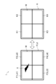
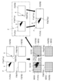
- FIG. 1 shows a schematic diagram of a defect classification method using an automatic defect classification device.
- FIG. 2 shows the combination of the first field of view and the second field of view when a defect occurring in an object to be inspected straddles both the first field of view and the second field of view.
- FIG. 3 shows a combination of the first field of view, the second field of view, and the third field of view in the case where a defect X straddles the first field of view, the second field of view, and the third field of view.
- (Defect Classification) 1 shows a schematic diagram of a defect classification method using an automatic defect classification apparatus 1.
- the automatic defect classification apparatus 1 classifies patterns of defects X that occur in an object to be inspected W.
- the object to be inspected W is the surface of a semiconductor wafer (substrate) in a semiconductor manufacturing process.
- a defect detection device detects defect X.
- an image of the inspected object W is captured by a camera (not shown) connected to an optical microscope or scanning electron microscope to obtain an inspection image J, and the inspection image J is compared with a reference image K.
- the reference image K is also called a fitting image or a statistically acceptable image.
- the reference image K is obtained, for example, by averaging images of the inspected object W that has been determined to be acceptable.
- the reference image K is set in advance.
- the inspection image J is superimposed on the reference image K.
- the automatic defect classification device 1 classifies the pattern of defect X only for the inspected object W in which defect X has been detected by the defect detection device.
- defect X patterns include foreign matter, scratches, poor edge rinsing, through-hole abnormalities, uneven coating, peeling, scratches, bonding pad abnormalities, uneven color, pattern abnormalities, stains, discoloration, deformation, etc.
- the automatic defect classification device 1 is composed of, for example, a microcomputer and a program.
- the automatic defect classification device 1 classifies the pattern of defect X based on a predetermined feature amount of defect X for inspection image J of inspected object W.
- the feature amount of defect X may be, for example, area, brightness, color, luminance, shape, sharpness, length, width, width/length, angle, transparency, etc.
- the feature amount of defect X is pre-registered in the automatic defect classification device 1.
- the automatic defect classification device 1 performs AI (Artificial Intelligence) on the inspection image J of the inspection object W.
- AI learning Artificial Intelligence
- the pattern of defect X may be classified based on classification conditions generated by AI learning.
- AI learning include machine learning and deep learning.
- machine learning include "supervised learning”, “unsupervised learning”, and “reinforcement learning”.
- the object W to be inspected is usually larger than the field of view (imaging range) F of the camera. Therefore, the object W to be inspected is imaged so as to be partitioned into a plurality of fields of view F. As a result, an inspection image J is obtained for each of the plurality of fields of view F.
- Each field of view F (each test image J) is adjacent to one another.
- each field of view F is rectangular.
- Each field of view F is arranged in a rectangular grid. In other words, each field of view F is adjacent to one another vertically and horizontally.
- the multiple fields of view F are exemplified as a first field of view F1 at the upper left, a second field of view F2 at the upper right, a third field of view F3 at the lower left, and a fourth field of view F4 at the lower right.
- the first field of view F1 and the second field of view F2 are adjacent in the left-right direction and share a left-right edge.
- the first field of view F1 and the third field of view F3 are adjacent in the up-down direction and share a top-down edge.
- the first field of view F1 and the fourth field of view F4 are adjacent diagonally up-down and left-right, but do not share any edges.
- the camera obtains four inspection images J1 to J4 corresponding to the four fields of view F1 to F4. Specifically, the camera obtains a first inspection image J1 corresponding to the first field of view F1, a second inspection image J2 corresponding to the second field of view F2, a third inspection image J3 corresponding to the third field of view F3, and a fourth inspection image J4 corresponding to the fourth field of view F4.
- the reference image K is similar to the inspection image J.
- four reference images K1 to K4 are prepared in advance to correspond to the four fields of view F1 to F4.
- a first reference image K1 corresponding to the first field of view F1 a second reference image K2 corresponding to the second field of view F2, a third reference image K3 corresponding to the third field of view F3, and a fourth reference image K4 corresponding to the fourth field of view F4 are prepared.
- a defect X that occurs in the object W to be inspected may span multiple fields of view F (inspection images J).
- the defect X that occurs in the object W to be inspected spans the left-right direction between the first field of view F1 (first inspection image J1) and the second field of view F2 (second inspection image J2).
- the defect X extends from the center in the first visual field F1 (first inspection image J1) to the right end of the outer periphery, and then extends slightly to the vicinity of the left end of the outer periphery in the second visual field F2 (second inspection image J2).
- the defect X has a jagged shape like the teeth of a saw.
- the defect detection device detects the defect X in the first visual field F1 (first inspection image J1) and the second visual field F2 (second inspection image J2) of the inspected object W.
- the defect detection device does not detect the defect X in the third visual field F3 (third inspection image J3) and the fourth visual field F4 (fourth inspection image J4) of the inspected object W. Note that the defect X does not exist in any of the four reference images K1 to K4.
- the automatic defect classification device When classifying the pattern of defect X by the automatic defect classification device 1, only the field of view F (inspection image J) in which defect X is detected by the defect detection device is extracted and compared with the reference image K.
- the first field of view F1 (first inspection image J1) and the second field of view F2 (second inspection image J2) are first extracted as the field of view F (inspection image J) in which defect X is detected. Then, the first field of view F1 (first inspection image J1) is compared with the first reference image K1, and the second field of view F2 (second inspection image J2) is compared with the second reference image K2.
- defect X is only faintly visible in the first field of view F1 (first inspection image J1) just as it is in the second field of view F2 (second inspection image J2), then it will be impossible to grasp the true features of defect X, and the accurate pattern of defect X will not be able to be grasped.
- the automatic defect classification device 1 makes it possible to accurately classify the pattern of defect X even when the defect X occurring in the object W to be inspected spans multiple fields of view F (inspection images J) by implementing the following measures.
- FIG. 2 shows a combination of a first field of view F1 and a second field of view F2 in a case where a defect X occurring in an object to be inspected W straddles both the first field of view F1 and the second field of view F2.
- the first field of view F1 is an arbitrary field of view FA, which is one field of view F arbitrarily selected from the multiple fields of view F (first field of view F1, second field of view F2, third field of view F3, and fourth field of view F4).
- the second field of view F2 is an adjacent field of view FB, which is another field of view adjacent to the arbitrary field of view FA (first field of view F1) from the multiple fields of view F (first field of view F1, second field of view F2, third field of view F3, and fourth field of view F4).
- other candidates for the adjacent field of view FB include a third field of view F3 adjacent to the first field of view F1 (arbitrary field of view FA) in the vertical direction, and a fourth field of view F4 adjacent to the first field of view F1 (arbitrary field of view FA) diagonally above, below, left, and right; however, since no defect X has been detected in these, they will be excluded this time (this will be described later when explaining memory 2).
- the automatic defect classification device 1 classifies the pattern of defect X in a state where the first field of view F1 (arbitrary field of view FA) and the second field of view F2 (adjacent field of view FB) are combined only when defect X is included in the outer periphery F1a (right end F1b) of the first field of view F1 (arbitrary field of view FA) on the side of the second field of view F2 (adjacent field of view FB) and defect X is included in the outer periphery F2a (left end F2b) of the second field of view F2 (adjacent field of view FB) on the side of the first field of view F1 (arbitrary field of view FA).
- the automatic defect classification device 1 classifies the pattern of defect X only when defect X is included on the shared edges (right end F1b and left end F2b) of the first field of view F1 (arbitrary field of view FA) and the second field of view F2 (adjacent field of view FB).
- the automatic defect classification device 1 stores the first field F1 (arbitrary field FA) and the second field F2 (adjacent field FB) in memory 2 described below, but does not combine the first field F1 (arbitrary field FA) and the second field F2 (adjacent field FB).
- the first field of view F1 (arbitrary field of view FA) is divided into a number of pixels G.
- the second field of view F2 (adjacent field of view FB) is divided into a number of pixels G.
- the same is true for the third field of view F3 and the fourth field of view F4.
- Pixel G is composed of two values: a value G1 indicating a state in which defect X is included, and a value G0 indicating a state in which defect X is not included.
- the value G1 indicating a state in which defect X is included and the value G0 indicating a state in which defect X is not included are distinguished, for example, based on a predetermined threshold value (or range) based on the luminance (0 to 255) of pixel G.
- the automatic defect classification device 1 classifies the pattern of defect X in a state where the first field of view F1 (arbitrary field of view FA) and the second field of view F2 (adjacent field of view FB) are combined only when a defect X is contained (value G1) in pixel G of the outer periphery F1a (right end F1b) on the side of the second field of view F2 (adjacent field of view FB) in the first field of view F1 (arbitrary field of view FA) and a defect X is contained (value G1) in pixel G of the outer periphery F2a (left end F2b) on the side of the first field of view F1 (arbitrary field of view FA) in the second field of view F2 (adjacent field of view FB).
- the defect X reflected in the first field of view F1 (arbitrary field of view FA) and the defect X reflected in the second field of view F2 (adjacent field of view FB) do not necessarily have to be adjacent in pixel G units.
- memory 2 is, for example, a known RAM.
- the automatic defect classification device 1 stores the first field of view F1 (arbitrary field of view FA) in the memory 2 when a pixel G on the outer periphery F1a (right end F1b) of the first field of view F1 (arbitrary field of view FA) on the side of the second field of view F2 (adjacent field of view FB) contains a defect X (value G1).
- the automatic defect classification device 1 stores the second field of view F2 (adjacent field of view FB) in memory 2 when a defect X is included (value G1) in the outer periphery F2a (left end F2b) of the second field of view F2 (adjacent field of view FB) on the side of the first field of view F1 (arbitrary field of view FA).
- the automatic defect classification device 1 does not store the third field of view F3 in the memory 2 because the third field of view F3 as the adjacent field of view FB does not include a defect X (value G0) on the outer periphery F3a (upper end F3b) on the side of the first field of view F1 (arbitrary field of view FA).
- the automatic defect classification device 1 does not store the fourth field of view F4 in the memory 2 because the fourth field of view F4 as the adjacent field of view FB does not contain a defect X (value G0) on the outer periphery F4a (upper left end F4b) on the side of the first field of view F1 (arbitrary field of view FA).
- the automatic defect classification device 1 outputs (calls) the first field of view F1 (arbitrary field of view FA) and the second field of view F2 (adjacent field of view FB) from the memory 2, and classifies the pattern of defect X with the first field of view F1 (arbitrary field of view FA) and the second field of view F2 (adjacent field of view FB) combined.
- the arbitrary visual field FA is the first visual field F1
- the arbitrary visual field FA first visual field F1
- the adjacent visual field FB second visual field F2
- the arbitrary visual field FA is then replaced with the second visual field F2, the third visual field F3, and the fourth visual field F4, and the same procedure is repeated.
- the first field of view F1 (arbitrary field of view FA) and the second field of view F2 (adjacent field of view FB) are adjacent to each other in the image of the inspection target W.
- a defect X is included in the outer periphery F1a of the first field of view F1 (arbitrary field of view FA) and a defect X is included in the outer periphery F2a of the second field of view F2 (adjacent field of view FB)
- the pattern of the defect X is classified in a state where the first field of view F1 (arbitrary field of view FA) and the second field of view F2 (adjacent field of view FB) are combined.
- the pattern of defect X is classified with the first field of view F1 (arbitrary field of view FA) and the second field of view F2 (adjacent field of view FB) combined, so even if defect X that has occurred in the inspected object W straddles both the first field of view F1 (arbitrary field of view FA) and the second field of view F2 (adjacent field of view FB), the original characteristic amount of defect X can be grasped.
- the pattern of defect X occurring in the object W to be inspected can be classified with high accuracy.
- a defect X is included in the outer periphery F1a (right edge F1b) of the first field of view F1 (arbitrary field of view FA) on the side of the second field of view F2 (adjacent field of view FB) and a defect X is included in the outer periphery F2a (left edge F2b) of the second field of view F2 (adjacent field of view FB) on the side of the first field of view F1 (arbitrary field of view FA), there is a high possibility that the defect X straddles both the first field of view F1 (arbitrary field of view FA) and the second field of view F2 (adjacent field of view FB).
- first field of view F1 arbitrary field of view FA
- second field of view F2 adjacent field of view FB
- the presence or absence of defect X in the outer periphery F1a, F2a of each field of view F1, F2 (FA, FB) can be clearly defined by the presence or absence of defect X in pixel G.
- each pixel G By configuring each pixel G with two values G0 and G1, it is possible to clarify whether each pixel G contains a defect X or not.
- the original feature quantity of the defect X that has occurred in the object to be inspected W can be grasped.
- Each field of view F1, F2 (FA, FB) is stored in memory 2 only if the outer periphery F1a, F2a of each field of view F1, F2 (FA, FB) contains a defect X, so the burden on memory 2 is small.
- the pattern of defect X may be classified with the first field of view F1 (arbitrary field of view FA) and the second field of view F2 (adjacent field of view FB) first combined.
- the defect X reflected at the left end of the first field of view F1 (arbitrary field of view FA) and the defect X reflected at the right end of the second field of view F2 (adjacent field of view FB) will be determined to be separate from each other (the two are not connected).
- the first field of view F1 (arbitrary field of view FA) and the fourth field of view F4 (adjacent field of view FB) may be stored in memory 2 but may not be combined with each other. This is because it is difficult to perform image processing to combine the first field of view F1 (arbitrary field of view FA) and the fourth field of view F4 (adjacent field of view FB) at their four corners.
- the defect X only straddles between the first field of view F1 as the arbitrary field of view FA and the second field of view F2 as the adjacent field of view FB, but is not limited to this. As shown in FIG. 3, the defect X may straddle the first field of view F1 as the arbitrary field of view FA, the second field of view F2 as the adjacent field of view FB, and the third field of view F3 as the adjacent field of view FB.
- the pattern X of the defect X is classified in a state where the first field of view F1 (arbitrary field of view FA), the second field of view F2 (adjacent field of view FB), and the third field of view F3 (adjacent field of view FB) are combined.
- the arbitrary visual field FA is the second visual field F2
- the candidates for the adjacent visual field FB are the first visual field F1, the third visual field F3, and the fourth visual field F4.
- the field of view F is not limited to a rectangle, but may be a polygon other than a rectangle, or a shape other than a polygon.
- the object W to be inspected is not limited to a semiconductor wafer, and various objects are possible.
- the object W to be inspected may be, for example, glass, metal, resin, etc.
- the object W to be inspected does not have to be a plate material, and may be, for example, an electric wire, etc.
- the defect classification method classifies the pattern of defect X that has occurred in an object W to be inspected.
- the object W to be inspected is imaged so as to be partitioned into a plurality of adjacent fields of view F.
- this defect classification method when a defect X is included in the outer periphery F1a of a first field F1 as an arbitrary field of view FA that is one field F among the plurality of fields of view F, and a defect X is included in the outer periphery F2a of a second field F2 as an adjacent field of view FB that is another field F adjacent to the first field F1 (arbitrary field of view FA) among the plurality of fields of view F, the pattern of defect X is classified in a state in which the first field F1 (arbitrary field of view FA) and the second field F2 (adjacent field of view FB) are combined.
- This disclosure is extremely useful and has high industrial applicability because it can be applied to defect classification devices and defect classification methods.
Landscapes
- Physics & Mathematics (AREA)
- Health & Medical Sciences (AREA)
- Life Sciences & Earth Sciences (AREA)
- Chemical & Material Sciences (AREA)
- Analytical Chemistry (AREA)
- Biochemistry (AREA)
- General Health & Medical Sciences (AREA)
- General Physics & Mathematics (AREA)
- Immunology (AREA)
- Pathology (AREA)
- Investigating Materials By The Use Of Optical Means Adapted For Particular Applications (AREA)
- Image Analysis (AREA)
Abstract
被検査対象に発生した欠陥のパターンを精度よく分類することにある。 具体的には、自動欠陥分類装置1は、被検査対象Wに発生した欠陥Xのパターンを分類する。被検査対象Wは、互いに隣接した複数の視野Fに区画されるように、撮像されている。自動欠陥分類装置1は、複数の視野Fのうちの一の視野Fである任意視野FAとしての第1視野F1の外周F1aに欠陥Xが含まれ且つ複数の視野Fのうちの第1視野F1(任意視野FA)に隣接する他の視野Fである隣接視野FBとしての第2視野F2の外周F2aに欠陥Xが含まれる場合に、第1視野F1(任意視野FA)と第2視野F2(隣接視野FB)とを結合した状態にて欠陥Xのパターンを分類する。
Description
本開示は、欠陥分類装置及び欠陥分類方法に関する。
例えば、半導体デバイスの製造工程では、半導体ウエハ(基板)の表面に露光、現像、エッチング等の処理を行うことによって、半導体ウエハ表面に多数の回路パターンを形成する。そして、多数の回路パターンが形成された半導体ウエハを、複数のチップ部品として個片化する。個片化されたチップ部品は、パッケージングされた後、電子部品単体として出荷されたり、電気製品に組み込まれたりする。
ここで、半導体ウエハが複数のチップ部品として個片化される前に、半導体ウエハ表面に対して、欠陥の検出が行われる。欠陥の検出は、例えば、光学顕微鏡や走査電子顕微鏡に接続されたカメラにより撮像された検査画像に基づいて、行われる。
そして、欠陥の検出された半導体ウエハに対して、欠陥の形状やサイズや色などの特徴量に基づいて、欠陥パターンの分類が行われる。欠陥パターンとして、例えば、異物や傷などがある。
従来、欠陥パターンの分類は、作業者による目視検査によって行われてきた。しかしながら、目視検査では、作業者の主観に応じて、欠陥パターンの分類結果にバラツキが生じ得るので、欠陥パターンを精度よく分類することができなかった。
そこで、特許文献1に示すように、半導体ウエハ表面に発生した欠陥パターンを自動的に分類する自動欠陥分類装置(Automatic Defect Classification:ADC)が、知られている。
しかしながら、特許文献1に係る自動欠陥分類装置を用いて、作業者の主観を排して欠陥パターンを分類したとしても、依然として、欠陥パターンの分類精度に課題がある。
被検査対象である半導体ウエハは、通常、カメラの視野(撮像範囲)よりも大きい。そこで、半導体ウエハを複数の視野に区画してカメラで撮像することによって、複数の視野毎に検査画像を得る。このとき、半導体ウエハに発生した欠陥が、複数の視野に亘って跨ることがある。
このため、1つの視野のみに基づいて欠陥パターンを分類しようとすると、欠陥パターンを正確に分類できないことがある。例えば、当該1つの視野の外周に僅かに一部だけ欠陥が映っている場合、一部だけ映された欠陥の本来の特徴量(形状やサイズや色など)を十分に把握できないので、正確な欠陥パターンを把握することができない。
上記課題は、半導体ウエハ以外の他の被検査対象にも、当てはまる。
本開示は斯かる点に鑑みてなされたものであり、その目的とするところは、被検査対象に発生した欠陥のパターンを精度よく分類することにある。
本開示に係る欠陥分類装置は、被検査対象に発生した欠陥のパターンを分類する欠陥分類装置であって、前記被検査対象は、互いに隣接した複数の視野に区画されるように撮像されており、複数の前記視野のうちの一の前記視野である任意視野の外周に前記欠陥が含まれ且つ複数の前記視野のうちの前記任意視野に隣接する他の前記視野である隣接視野の前記外周に前記欠陥が含まれる場合に、前記任意視野と前記隣接視野とを結合した状態にて前記欠陥の前記パターンを分類する。
撮像される被検査対象において、任意視野と隣接視野とは、互いに隣接している。任意視野の外周に欠陥が含まれ且つ隣接視野の外周に欠陥が含まれる場合、任意視野と隣接視野とが結合された状態にて欠陥のパターンが分類される。
このように、任意視野と隣接視野とが結合された状態にて欠陥のパターンが分類されるので、被検査対象に発生した欠陥が任意視野と隣接視野とに亘って跨っている場合であっても、欠陥の本来の特徴量を把握することができる。
以上、被検査対象に発生した欠陥のパターンを精度よく分類することができる。
一実施形態では、前記任意視野における前記隣接視野側の前記外周に前記欠陥が含まれ且つ前記隣接視野における前記任意視野側の前記外周に前記欠陥が含まれる場合に、前記任意視野と前記隣接視野とを結合した状態にて前記欠陥の前記パターンを分類する。
任意視野における隣接視野側の外周に欠陥が含まれ且つ隣接視野における任意視野側の外周に欠陥が含まれる場合、ある欠陥が任意視野と隣接視野とに亘って跨っている可能性が高い。このような場合に任意視野と隣接視野とを結合することによって、任意視野と隣接視野とに亘って跨る欠陥の全体像を把握する上で有利になる。
一実施形態では、前記任意視野は、複数の画素に区画されており、前記隣接視野は、複数の前記画素に区画されており、前記任意視野における前記外周の前記画素に前記欠陥が含まれ且つ前記隣接視野における前記外周の前記画素に前記欠陥が含まれる場合に、前記任意視野と前記隣接視野とを結合した状態にて前記欠陥の前記パターンを分類する。
各視野の外周における欠陥の有無を、画素における欠陥の有無によって、より明確に定義することができる。
一実施形態では、前記画素は、前記欠陥が含まれる状態を示す値と前記欠陥が含まれない状態を示す値との2値で構成されている。
各画素を2値で構成することによって、各画素に欠陥が含まれるか否かを明確にすることができる。
一実施形態では、前記隣接視野は、前記任意視野の上下左右の少なくともいずれかに配置されている。
欠陥が、任意視野と上下左右の少なくともいずれかの隣接視野とに亘って跨る場合であっても、被検査対象に発生した欠陥の本来の特徴量を把握することができる。
一実施形態では、前記任意視野の前記外周に前記欠陥が含まれる場合に、前記任意視野をメモリに記憶して、前記隣接視野の前記外周に前記欠陥が含まれる場合に、前記隣接視野を前記メモリに記憶して、前記任意視野と前記隣接視野とを前記メモリから出力して、前記任意視野と前記隣接視野とを結合した状態にて前記欠陥の前記パターンを分類する。
各視野の外周に欠陥が含まれる場合のみに、各視野がメモリに記憶されるので、メモリへの負担が少ない。
本開示に係る欠陥分類方法は、被検査対象に発生した欠陥のパターンを分類する欠陥分類方法であって、前記被検査対象は、互いに隣接した複数の視野に区画されるように撮像されており、複数の前記視野のうちの一の前記視野である任意視野の外周に前記欠陥が含まれ且つ複数の前記視野のうちの前記任意視野に隣接する他の前記視野である隣接視野の前記外周に前記欠陥が含まれる場合に、前記任意視野と前記隣接視野とを結合した状態にて前記欠陥の前記パターンを分類する。
本開示によれば、被検査対象に発生した欠陥のパターンを精度よく分類することができる。
以下、本開示の一実施形態を図面に基づいて詳細に説明する。以下の好ましい実施形態の説明は、本質的に例示に過ぎず、本開示、その適用物あるいはその用途を制限することを意図するものでは全くない。
(欠陥分類)
図1は、自動欠陥分類装置1による欠陥分類方法を模式的に示す。自動欠陥分類装置1は、被検査対象Wに発生した欠陥Xのパターンを、分類する。本例では、被検査対象Wは、半導体製造工程における半導体ウエハ(基板)の表面である。
図1は、自動欠陥分類装置1による欠陥分類方法を模式的に示す。自動欠陥分類装置1は、被検査対象Wに発生した欠陥Xのパターンを、分類する。本例では、被検査対象Wは、半導体製造工程における半導体ウエハ(基板)の表面である。
自動欠陥分類装置1による欠陥Xのパターンの分類工程の前工程において、欠陥検出装置(図示せず)による欠陥Xの検出が行われる。欠陥Xの検出にあたって、光学顕微鏡や走査電子顕微鏡に接続されたカメラ(図示せず)によって被検査対象Wを撮像して検査画像Jを得るとともに、検査画像Jを基準画像Kと比較する。
基準画像Kは、フィッティング画像や統計的良品画像とも呼ばれる。基準画像Kは、例えば、良品判定された被検査対象Wの画像を平均化することによって、得られる。基準画像Kは、事前に設定されている。欠陥Xの検出にあたって、検査画像Jを、基準画像Kに重ね合わせる。
自動欠陥分類装置1は、欠陥検出装置により欠陥Xが検出された被検査対象Wについてのみ、欠陥Xのパターンを分類する。ここで、欠陥Xのパターンとして、例えば、異物、傷、エッジリンス不良、スルーホール異常、塗膜ムラ、剥がれ、スクラッチ、ボンディングパッド異常、色ムラ、パターン異常、染み、変色、変形、などがある。
自動欠陥分類装置1は、例えば、マイコン及びプログラムで構成されている。自動欠陥分類装置1は、被検査対象Wの検査画像Jに対して、欠陥Xにおける所定の特徴量に基づいて、欠陥Xのパターンを分類する。欠陥Xの特徴量として、例えば、面積、明るさ、色、輝度、形状、鮮明さ、長さ、幅、幅/長さ、角度、透明度、などがある。自動欠陥分類装置1には、欠陥Xの特徴量が、事前に登録されている。
また、自動欠陥分類装置1は、被検査対象Wの検査画像Jに対して、AI(Artificial
Intelligence)学習により生成された分類条件に基づいて、欠陥Xのパターンを分類してもよい。AI学習として、例えば、機械学習やディープラーニング等がある。また、機械学習として、「教師有り学習」、「教師無し学習」及び「強化学習」等がある。
Intelligence)学習により生成された分類条件に基づいて、欠陥Xのパターンを分類してもよい。AI学習として、例えば、機械学習やディープラーニング等がある。また、機械学習として、「教師有り学習」、「教師無し学習」及び「強化学習」等がある。
(視野の区画)
ここで、被検査対象Wは、通常、カメラの視野(撮像範囲)Fよりも大きい。そこで、被検査対象Wは、複数の視野Fに区画されるように、撮像される。これにより、複数の視野F毎に検査画像Jが得られる。
ここで、被検査対象Wは、通常、カメラの視野(撮像範囲)Fよりも大きい。そこで、被検査対象Wは、複数の視野Fに区画されるように、撮像される。これにより、複数の視野F毎に検査画像Jが得られる。
各視野F(各検査画像J)は、互いに隣接している。本例では、各視野Fは、四角形である。各視野Fは、四角形の格子状に並んでいる。換言すると、各視野Fは、上下左右に互いに隣接している。
図1では、複数の視野Fとして、左上の第1視野F1、右上の第2視野F2、左下の第3視野F3及び右下の第4視野F4を、例示する。第1視野F1と第2視野F2とは、左右方向に隣接しており、左右の辺を共有している。第1視野F1と第3視野F3とは、上下方向に隣接しており、上下の辺を共有している。第1視野F1と第4視野F4とは、斜め上下左右に隣接しているが、いずれの辺をも共有していない。
カメラによって、4つの視野F1~F4に対応するように、4つの検査画像J1~J4が得られる。具体的には、第1視野F1に対応する第1検査画像J1、第2視野F2に対応する第2検査画像J2、第3視野F3に対応する第3検査画像J3及び第4視野F4に対応する第4検査画像J4が、カメラによって得られる。
基準画像Kも、検査画像Jと同様である。すなわち、4つの視野F1~F4に対応するように、4つの基準画像K1~K4が予め用意されている。具体的には、第1視野F1に対応する第1基準画像K1、第2視野F2に対応する第2基準画像K2、第3視野F3に対応する第3基準画像K3及び第4視野F4に対応する第4基準画像K4が、用意されている。
ここで、被検査対象Wに発生した欠陥Xが、複数の視野F(検査画像J)に亘って跨ることがある。図1では、被検査対象Wに発生した欠陥Xは、第1視野F1(第1検査画像J1)と第2視野F2(第2検査画像J2)とに亘って左右方向に跨っている。
図1に示すように、欠陥Xは、第1視野F1(第1検査画像J1)における中央部から外周の右端まで延びた後に、第2視野F2(第2検査画像J2)における外周の左端付近に僅かに至っている。欠陥Xには、ノコギリの歯のようなギザギザの形状がある
ここで、欠陥検出装置は、被検査対象Wにおける第1視野F1(第1検査画像J1)及び第2視野F2(第2検査画像J2)において、欠陥Xを検出する。一方、欠陥検出装置は、被検査対象Wにおける第3視野F3(第3検査画像J3)及び第4視野F4(第4検査画像J4)において、欠陥Xを検出しない。なお、4つの基準画像K1~K4のいずれにも、欠陥Xは存在しない。
ここで、欠陥検出装置は、被検査対象Wにおける第1視野F1(第1検査画像J1)及び第2視野F2(第2検査画像J2)において、欠陥Xを検出する。一方、欠陥検出装置は、被検査対象Wにおける第3視野F3(第3検査画像J3)及び第4視野F4(第4検査画像J4)において、欠陥Xを検出しない。なお、4つの基準画像K1~K4のいずれにも、欠陥Xは存在しない。
自動欠陥分類装置1による欠陥Xのパターンの分類では、欠陥検出装置により欠陥Xの検出された視野F(検査画像J)のみを、抽出して、基準画像Kと比較する。本例では、欠陥Xの検出された視野F(検査画像J)として、第1視野F1(第1検査画像J1)及び第2視野F2(第2検査画像J2)が、先ず抽出される。そして、第1視野F1(第1検査画像J1)が第1基準画像K1と比較されるとともに、第2視野F2(第2検査画像J2)が第2基準画像K2と比較される。
1つの視野Fのみに基づいて欠陥Xのパターンを分類しようとすると、欠陥Xのパターンを正確に分類できないことがある。例えば、第2視野F2(第2検査画像J2)には、その外周の左端付近に僅かにしか欠陥Xが映っていない。このため、第2視野F2(第2検査画像J2)を第2基準画像K2と比較したとしても、欠陥Xの本来の特徴量(形状やサイズや色など)を十分に把握できず、正確な欠陥Xのパターンを把握することができない。
一方、第1視野F1(第1検査画像J1)には、その中央部から外周の右端に亘って大部分で欠陥Xが映っている。このため、第1視野F1(第1検査画像J1)を第1基準画像K1と比較した場合、欠陥Xの本来の特徴量を把握できるかもしれず、正確な欠陥Xのパターンを把握できるかもしれない。例えば、第1視野F1(第1検査画像J1)に映る欠陥Xにおけるギザギザの形状に基づいて、欠陥Xのパターンを「傷」と分類できるかもしれない。
しかしながら、仮に、第1視野F1(第1検査画像J1)にも、第2視野F2(第2検査画像J2)と同様に僅かにしか欠陥Xが映っていなければ、やはり欠陥Xの本来の特徴量を把握できず、正確な欠陥Xのパターンを把握できないであろう。
このように、被検査対象Wに発生した欠陥Xが複数の視野F(検査画像J)に亘って跨る場合に、欠陥Xのパターンを精度よく分類することは難しい。
本実施形態に係る自動欠陥分類装置1では、以下の工夫を施すことによって、被検査対象Wに発生した欠陥Xが複数の視野F(検査画像J)に亘って跨る場合であっても、欠陥Xのパターンを精度よく分類することを可能にした。
(欠陥の結合)
図2は、被検査対象Wに発生した欠陥Xが第1視野F1と第2視野F2とに亘って跨る場合における第1視野F1と第2視野F2との結合を示す。
図2は、被検査対象Wに発生した欠陥Xが第1視野F1と第2視野F2とに亘って跨る場合における第1視野F1と第2視野F2との結合を示す。
第1視野F1は、複数の視野F(第1視野F1、第2視野F2、第3視野F3及び第4視野F4)のうちの任意に選択された一の視野Fである任意視野FAとする。第2視野F2は、複数の視野F(第1視野F1、第2視野F2、第3視野F3及び第4視野F4)のうちの任意視野FA(第1視野F1)に隣接する他の視野である隣接視野FBとする。
なお、隣接視野FBの候補として、第2視野F2の他にも、第1視野F1(任意視野FA)に上下方向に隣接する第3視野F3と、第1視野F1(任意視野FA)に斜め上下左右に隣接する第4視野F4とがあるが、これらには欠陥Xが検出されていないので今回は除外する(メモリ2の説明の際に後述する)。
隣接視野FBは、任意視野FAの上下左右の少なくともいずれかに配置されている。本例では、隣接視野FBとしての第2視野F2は、任意視野FAとしての第1視野F1の右側に配置されている。
自動欠陥分類装置1は、第1視野F1(任意視野FA)の外周F1aに欠陥Xが含まれ且つ第2視野F2(隣接視野FB)の外周F2aに欠陥Xが含まれる場合に、第1視野F1(任意視野FA)と第2視野F2(隣接視野FB)とを結合した状態にて、欠陥Xのパターンを分類する。
詳細には、自動欠陥分類装置1は、第1視野F1(任意視野FA)における第2視野F2(隣接視野FB)側の外周F1a(右端F1b)に欠陥Xが含まれ且つ第2視野F2(隣接視野FB)における第1視野F1(任意視野FA)側の外周F2a(左端F2b)に欠陥Xが含まれる場合のみに、第1視野F1(任意視野FA)と第2視野F2(隣接視野FB)とを結合した状態にて、欠陥Xのパターンを分類する。
換言すると、自動欠陥分類装置1は、第1視野F1(任意視野FA)及び第2視野F2(隣接視野FB)における互いに共有する辺同士(右端F1b及び左端F2b)に欠陥Xが含まれる場合のみに、欠陥Xのパターンを分類する。
また、第1視野F1(任意視野FA)における第2視野F2(隣接視野FB)側の外周F1a(右端F1b)に欠陥Xが含まれるとしても、第2視野F2(隣接視野FB)における第1視野F1(任意視野FA)側の外周F2a(左端F2b)に欠陥Xが含まれない場合には、自動欠陥分類装置1は、第1視野F1(任意視野FA)及び第2視野F2(隣接視野FB)を後述のメモリ2に記憶しつつも、第1視野F1(任意視野FA)と第2視野F2(隣接視野FB)とを結合しない。
より詳細には、第1視野F1(任意視野FA)は、複数の画素Gに区画されている。第2視野F2(隣接視野FB)は、複数の画素Gに区画されている。第3視野F3及び第4視野F4についても、同様である。
画素Gは、欠陥Xが含まれる状態を示す値G1と欠陥Xが含まれない状態を示す値G0との2値で構成されている。欠陥Xが含まれる状態を示す値G1と欠陥Xが含まれない状態を示す値G0とは、例えば、画素Gにおける輝度(0~255)に基づいて所定の閾値(又は範囲)を基準に区分けされる。
そして、自動欠陥分類装置1は、第1視野F1(任意視野FA)における第2視野F2(隣接視野FB)側の外周F1a(右端F1b)の画素Gに欠陥Xが含まれ(値G1)且つ第2視野F2(隣接視野FB)における第1視野F1(任意視野FA)側の外周F2a(左端F2b)の画素Gに欠陥Xが含まれる(値G1)場合のみに、第1視野F1(任意視野FA)と第2視野F2(隣接視野FB)とを結合した状態にて、欠陥Xのパターンを分類する。
第1視野F1(任意視野FA)に映る欠陥Xと、第2視野F2(隣接視野FB)に映る欠陥Xとは、必ずしも画素G単位で隣接しなくてもよい。
次に、メモリ2への各視野Fの記憶について説明する。なお、メモリ2は、例えば公知のRAMである。
自動欠陥分類装置1は、第1視野F1(任意視野FA)における第2視野F2(隣接視野FB)側の外周F1a(右端F1b)の画素Gに欠陥Xが含まれる(値G1)場合に、第1視野F1(任意視野FA)をメモリ2に記憶する。
同様に、自動欠陥分類装置1は、第2視野F2(隣接視野FB)における第1視野F1(任意視野FA)側の外周F2a(左端F2b)に欠陥Xが含まれる(値G1)場合に、第2視野F2(隣接視野FB)をメモリ2に記憶する。
一方、自動欠陥分類装置1は、隣接視野FBとしての第3視野F3における第1視野F1(任意視野FA)側の外周F3a(上端F3b)に欠陥Xが含まれない(値G0)ので、第3視野F3をメモリ2に記憶しない。
同様に、自動欠陥分類装置1は、隣接視野FBとしての第4視野F4における第1視野F1(任意視野FA)側の外周F4a(左上端F4b)に欠陥Xが含まれない(値G0)ので、第4視野F4をメモリ2に記憶しない。
そして、自動欠陥分類装置1は、第1視野F1(任意視野FA)と第2視野F2(隣接視野FB)とをメモリ2から出力(呼び出して)して、第1視野F1(任意視野FA)と第2視野F2(隣接視野FB)とを結合した状態にて欠陥Xのパターンを分類する。
なお、任意視野FAを第1視野F1とした場合における任意視野FA(第1視野F1)及び隣接視野FB(第2視野F2)のメモリ2への記憶が完了したら、次に、任意視野FAを、第2視野F2、第3視野F3及び第4視野F4に置き換えて、同様の手順を繰り返す。
(作用効果)
撮像される被検査対象Wにおいて、第1視野F1(任意視野FA)と第2視野F2(隣接視野FB)とは、互いに隣接している。第1視野F1(任意視野FA)の外周F1aに欠陥Xが含まれ且つ第2視野F2(隣接視野FB)の外周F2aに欠陥Xが含まれる場合、第1視野F1(任意視野FA)と第2視野F2(隣接視野FB)とが結合された状態にて欠陥Xのパターンが分類される。
撮像される被検査対象Wにおいて、第1視野F1(任意視野FA)と第2視野F2(隣接視野FB)とは、互いに隣接している。第1視野F1(任意視野FA)の外周F1aに欠陥Xが含まれ且つ第2視野F2(隣接視野FB)の外周F2aに欠陥Xが含まれる場合、第1視野F1(任意視野FA)と第2視野F2(隣接視野FB)とが結合された状態にて欠陥Xのパターンが分類される。
このように、第1視野F1(任意視野FA)と第2視野F2(隣接視野FB)とが結合された状態にて欠陥Xのパターンが分類されるので、被検査対象Wに発生した欠陥Xが第1視野F1(任意視野FA)と第2視野F2(隣接視野FB)とに亘って跨っている場合であっても、欠陥Xの本来の特徴量を把握することができる。
以上、被検査対象Wに発生した欠陥Xのパターンを精度よく分類することができる。
第1視野F1(任意視野FA)における第2視野F2(隣接視野FB)側の外周F1a(右端F1b)に欠陥Xが含まれ且つ第2視野F2(隣接視野FB)における第1視野F1(任意視野FA)側の外周F2a(左端F2b)に欠陥Xが含まれる場合、ある欠陥Xが第1視野F1(任意視野FA)と第2視野F2(隣接視野FB)とに亘って跨っている可能性が高い。
このような場合に第1視野F1(任意視野FA)と第2視野F2(隣接視野FB)とを結合することによって、第1視野F1(任意視野FA)と第2視野F2(隣接視野FB)とに亘って跨る欠陥Xの全体像を把握する上で有利になる。
各視野F1,F2(FA,FB)の外周F1a,F2aにおける欠陥Xの有無を、画素Gにおける欠陥Xの有無によって、明確に定義することができる。
各画素Gを2値G0,G1で構成することによって、各画素Gに欠陥Xが含まれるか否かを明確にすることができる。
欠陥Xが、任意視野FAと上下左右の少なくともいずれかの隣接視野FBとに亘って跨る場合であっても、被検査対象Wに発生した欠陥Xの本来の特徴量を把握することができる。
各視野F1,F2(FA,FB)の外周F1a,F2aに欠陥Xが含まれる場合のみに、各視野F1,F2(FA,FB)がメモリ2に記憶されるので、メモリ2への負担が少ない。
(その他の実施形態)
以上、本開示を好適な実施形態により説明してきたが、こうした記述は限定事項ではなく、勿論、種々の改変が可能である。
以上、本開示を好適な実施形態により説明してきたが、こうした記述は限定事項ではなく、勿論、種々の改変が可能である。
第1視野F1(任意視野FA)の外周F1aにおける左端に欠陥Xが含まれ且つ第2視野F2(隣接視野FB)の外周F2aにおける右端に欠陥Xが含まれる場合に、第1視野F1(任意視野FA)と第2視野F2(隣接視野FB)とを一先ず結合した状態にて、欠陥Xのパターンを分類してもよい。この場合、第1視野F1(任意視野FA)の左端に映る欠陥Xと、第2視野F2(隣接視野FB)の右端に映る欠陥Xとは、互いに別物である(両者は繋がっていない)と判断されるだろう。
第1視野F1(任意視野FA)の外周F1aにおける右下端に欠陥Xが含まれ且つ第4視野F4(隣接視野FB)の外周F4aにおける左上端F4bに欠陥Xが含まれる場合に、第1視野F1(任意視野FA)及び第4視野F4(隣接視野FB)をメモリ2に記憶しつつも、第1視野F1(任意視野FA)と第4視野F4(隣接視野FB)とを結合しなくてもよい。第1視野F1(任意視野FA)と第4視野F4(隣接視野FB)とを四隅同士で結合するように画像処理することは、難しいからである。
上記実施形態では、欠陥Xが、任意視野FAとしての第1視野F1と隣接視野FBとしての第2視野F2との間にのみ跨っているが、これに限定されない。図3に示すように、欠陥Xは、任意視野FAとしての第1視野F1と、隣接視野FBとしての第2視野F2と、隣接視野FBとしての第3視野F3と、に亘って跨ってもよい。
この場合、第1視野F1(任意視野FA)と第2視野F2(隣接視野FB)と第3視野F3(隣接視野FB)とが結合された状態にて、欠陥XのパターンXが分類される。
任意視野FAと隣接視野FBとの組合せは、複数ある。例えば、任意視野FAが第2視野F2である場合、隣接視野FBの候補として、第1視野F1、第3視野F3及び第4視野F4がある。
視野Fは、四角形に限定されず、四角形以外の多角形や、多角形以外の形状などでもよい。
被検査対象Wは、半導体ウエハに限定されず、種々の対象が考えられ得る。被検査対象Wは、例えば、ガラスや金属や樹脂等でもよい。被検査対象Wは、板材でなくてもよく、例えば電線等でもよい。
画素Gにおける欠陥Xの有無を判定するにあたって、例えば、色相、明度、暗度、彩度、光度、照度などの、その他の光学情報を参照してもよい。
本開示に係る欠陥分類方法は、被検査対象Wに発生した欠陥Xのパターンを分類する。この欠陥分類方法では、被検査対象Wは、互いに隣接した複数の視野Fに区画されるように、撮像されている。この欠陥分類方法では、複数の視野Fのうちの一の視野Fである任意視野FAとしての第1視野F1の外周F1aに欠陥Xが含まれ且つ複数の視野Fのうちの第1視野F1(任意視野FA)に隣接する他の視野Fである隣接視野FBとしての第2視野F2の外周F2aに欠陥Xが含まれる場合に、第1視野F1(任意視野FA)と第2視野F2(隣接視野FB)とを結合した状態にて欠陥Xのパターンを分類する。
本開示は、欠陥分類装置及び欠陥分類方法に適用できるので、極めて有用であり、産業上の利用可能性が高い。
W 被検査対象
X 欠陥
J 検査画像
J1 第1検査画像
J2 第2検査画像
J3 第3検査画像
J4 第4検査画像
K 基準画像
K1 第1基準画像
K2 第2基準画像
K3 第3基準画像
K4 第4基準画像
F 視野
F1 第1視野
F1a 外周
F1b 右端
F2 第2視野
F2a 外周
F2b 左端
F3 第3視野
F3a 外周
F3b 上端
F4 第4視野
F4a 外周
F4b 左上端
FA 任意視野
FB 隣接視野
G 画素
G0 値
G1 値
1 自動欠陥分類装置
2 メモリ
X 欠陥
J 検査画像
J1 第1検査画像
J2 第2検査画像
J3 第3検査画像
J4 第4検査画像
K 基準画像
K1 第1基準画像
K2 第2基準画像
K3 第3基準画像
K4 第4基準画像
F 視野
F1 第1視野
F1a 外周
F1b 右端
F2 第2視野
F2a 外周
F2b 左端
F3 第3視野
F3a 外周
F3b 上端
F4 第4視野
F4a 外周
F4b 左上端
FA 任意視野
FB 隣接視野
G 画素
G0 値
G1 値
1 自動欠陥分類装置
2 メモリ
Claims (7)
- 被検査対象に発生した欠陥のパターンを分類する欠陥分類装置であって、
前記被検査対象は、互いに隣接した複数の視野に区画されるように撮像されており、
複数の前記視野のうちの一の前記視野である任意視野の外周に前記欠陥が含まれ且つ複数の前記視野のうちの前記任意視野に隣接する他の前記視野である隣接視野の前記外周に前記欠陥が含まれる場合に、前記任意視野と前記隣接視野とを結合した状態にて前記欠陥の前記パターンを分類する、欠陥分類装置。 - 請求項1に記載の欠陥分類装置であって、
前記任意視野における前記隣接視野側の前記外周に前記欠陥が含まれ且つ前記隣接視野における前記任意視野側の前記外周に前記欠陥が含まれる場合に、前記任意視野と前記隣接視野とを結合した状態にて前記欠陥の前記パターンを分類する、欠陥分類装置。 - 請求項1又は2に記載の欠陥分類装置であって、
前記任意視野は、複数の画素に区画されており、
前記隣接視野は、複数の前記画素に区画されており、
前記任意視野における前記外周の前記画素に前記欠陥が含まれ且つ前記隣接視野における前記外周の前記画素に前記欠陥が含まれる場合に、前記任意視野と前記隣接視野とを結合した状態にて前記欠陥の前記パターンを分類する、欠陥分類装置。 - 請求項3に記載の欠陥分類装置であって、
前記画素は、前記欠陥が含まれる状態を示す値と前記欠陥が含まれない状態を示す値との2値で構成されている、欠陥分類装置。 - 請求項1に記載の欠陥分類装置であって、
前記隣接視野は、前記任意視野の上下左右の少なくともいずれかに配置されている、欠陥分類装置。 - 請求項1に記載の欠陥分類装置であって、
前記任意視野の前記外周に前記欠陥が含まれる場合に、前記任意視野をメモリに記憶して、
前記隣接視野の前記外周に前記欠陥が含まれる場合に、前記隣接視野を前記メモリに記憶して、
前記任意視野と前記隣接視野とを前記メモリから出力して、前記任意視野と前記隣接視野とを結合した状態にて前記欠陥の前記パターンを分類する、欠陥分類装置。 - 被検査対象に発生した欠陥のパターンを分類する欠陥分類方法であって、
前記被検査対象は、互いに隣接した複数の視野に区画されるように撮像されており、
複数の前記視野のうちの一の前記視野である任意視野の外周に前記欠陥が含まれ且つ複数の前記視野のうちの前記任意視野に隣接する他の前記視野である隣接視野の前記外周に前記欠陥が含まれる場合に、前記任意視野と前記隣接視野とを結合した状態にて前記欠陥の前記パターンを分類する、欠陥分類方法。
Applications Claiming Priority (2)
| Application Number | Priority Date | Filing Date | Title |
|---|---|---|---|
| JP2023-018602 | 2023-02-09 | ||
| JP2023018602A JP2024113537A (ja) | 2023-02-09 | 2023-02-09 | 欠陥分類装置及び欠陥分類方法 |
Publications (1)
| Publication Number | Publication Date |
|---|---|
| WO2024166609A1 true WO2024166609A1 (ja) | 2024-08-15 |
Family
ID=92262310
Family Applications (1)
| Application Number | Title | Priority Date | Filing Date |
|---|---|---|---|
| PCT/JP2024/000742 Ceased WO2024166609A1 (ja) | 2023-02-09 | 2024-01-15 | 欠陥分類装置及び欠陥分類方法 |
Country Status (3)
| Country | Link |
|---|---|
| JP (1) | JP2024113537A (ja) |
| TW (1) | TW202433626A (ja) |
| WO (1) | WO2024166609A1 (ja) |
Cited By (1)
| Publication number | Priority date | Publication date | Assignee | Title |
|---|---|---|---|---|
| CN121275777A (zh) * | 2025-12-09 | 2026-01-06 | 常州润来科技有限公司 | 一种非接触式铜管表面锯齿伤检测方法及系统 |
Citations (7)
| Publication number | Priority date | Publication date | Assignee | Title |
|---|---|---|---|---|
| JP2009025003A (ja) * | 2007-07-17 | 2009-02-05 | Nikon Corp | 表面状態検査装置 |
| US20160125583A1 (en) * | 2013-06-07 | 2016-05-05 | Asti Holdings Limited | Systems and methods for automatically verifying correct die removal from film frames |
| JP2018179563A (ja) * | 2017-04-04 | 2018-11-15 | 新日鐵住金株式会社 | 表面検査装置および表面検査方法 |
| JP2020148744A (ja) * | 2019-03-15 | 2020-09-17 | シャープ株式会社 | 画像処理装置、および、画像処理方法 |
| WO2021260263A1 (en) * | 2020-06-24 | 2021-12-30 | Procemex Oy | Smart synchronization method of a web inspection system |
| JP2022055953A (ja) * | 2020-09-29 | 2022-04-08 | タカノ株式会社 | 欠陥分類装置、欠陥分類方法及びプログラム |
| WO2022190636A1 (ja) * | 2021-03-12 | 2022-09-15 | オムロン株式会社 | 支援装置および方法 |
-
2023
- 2023-02-09 JP JP2023018602A patent/JP2024113537A/ja active Pending
-
2024
- 2024-01-15 WO PCT/JP2024/000742 patent/WO2024166609A1/ja not_active Ceased
- 2024-01-29 TW TW113103292A patent/TW202433626A/zh unknown
Patent Citations (7)
| Publication number | Priority date | Publication date | Assignee | Title |
|---|---|---|---|---|
| JP2009025003A (ja) * | 2007-07-17 | 2009-02-05 | Nikon Corp | 表面状態検査装置 |
| US20160125583A1 (en) * | 2013-06-07 | 2016-05-05 | Asti Holdings Limited | Systems and methods for automatically verifying correct die removal from film frames |
| JP2018179563A (ja) * | 2017-04-04 | 2018-11-15 | 新日鐵住金株式会社 | 表面検査装置および表面検査方法 |
| JP2020148744A (ja) * | 2019-03-15 | 2020-09-17 | シャープ株式会社 | 画像処理装置、および、画像処理方法 |
| WO2021260263A1 (en) * | 2020-06-24 | 2021-12-30 | Procemex Oy | Smart synchronization method of a web inspection system |
| JP2022055953A (ja) * | 2020-09-29 | 2022-04-08 | タカノ株式会社 | 欠陥分類装置、欠陥分類方法及びプログラム |
| WO2022190636A1 (ja) * | 2021-03-12 | 2022-09-15 | オムロン株式会社 | 支援装置および方法 |
Cited By (2)
| Publication number | Priority date | Publication date | Assignee | Title |
|---|---|---|---|---|
| CN121275777A (zh) * | 2025-12-09 | 2026-01-06 | 常州润来科技有限公司 | 一种非接触式铜管表面锯齿伤检测方法及系统 |
| CN121275777B (zh) * | 2025-12-09 | 2026-03-13 | 常州润来科技有限公司 | 一种非接触式铜管表面锯齿伤检测方法及系统 |
Also Published As
| Publication number | Publication date |
|---|---|
| JP2024113537A (ja) | 2024-08-22 |
| TW202433626A (zh) | 2024-08-16 |
Similar Documents
| Publication | Publication Date | Title |
|---|---|---|
| KR101192053B1 (ko) | 반도체 기판 이상들을 검출하기 위한 장치 및 방법 | |
| JP2010217169A (ja) | 印刷回路基板の外観検査システム及びその方法 | |
| KR20190003790A (ko) | 결합된 패치 및 설계 기반 결함 검출 | |
| WO2024166609A1 (ja) | 欠陥分類装置及び欠陥分類方法 | |
| KR20090008185A (ko) | 표면 검사 장치 | |
| JP2004109018A (ja) | 回路パターン検査方法および検査装置 | |
| US10466179B2 (en) | Semiconductor device inspection of metallic discontinuities | |
| KR102352698B1 (ko) | 자동화된 이미지 기반 프로세스 모니터링 및 제어 | |
| EP2063259A1 (en) | Method for inspecting mounting status of electronic component | |
| WO2010004914A1 (ja) | 致命傷の検出方法 | |
| JP7824801B2 (ja) | 欠陥検査装置及び欠陥検査方法 | |
| CN107256835A (zh) | 一种凸块缺陷检测方法 | |
| TWI679611B (zh) | 薄膜檢查方法 | |
| KR100673392B1 (ko) | 필름, 테이프 형태의 인쇄회로기판 외관 검사에서의 과검출방지를 위한 시스템 및 그 처리 방법 | |
| KR102737243B1 (ko) | 웨이퍼 결함 검출을 위한 투영 및 거리 분할 알고리즘 | |
| CN106248689B (zh) | 复合膜的缺陷判别方法 | |
| JP2013245985A (ja) | 欠陥検査装置、欠陥検査方法、及び欠陥検査プログラム | |
| JP5018182B2 (ja) | 半導体装置の製造方法 | |
| JP2025098638A (ja) | 欠陥分類装置 | |
| TW202339040A (zh) | 缺陷分類裝置 | |
| JP3803677B2 (ja) | 欠陥分類装置及び欠陥分類方法 | |
| KR102886462B1 (ko) | 패턴이 형상화되어 있는 표면 이물 연속 검출 및 이물 자동 세정 장치 | |
| KR20050117710A (ko) | 웨이퍼 결함 검출 방법 | |
| US20250086780A1 (en) | Concentricity offset measurement for hybrid bonding | |
| Yin | Analysis of optical inspection from aoi and avi machines |
Legal Events
| Date | Code | Title | Description |
|---|---|---|---|
| 121 | Ep: the epo has been informed by wipo that ep was designated in this application |
Ref document number: 24753055 Country of ref document: EP Kind code of ref document: A1 |
|
| NENP | Non-entry into the national phase |
Ref country code: DE |
|
| 122 | Ep: pct application non-entry in european phase |
Ref document number: 24753055 Country of ref document: EP Kind code of ref document: A1 |