WO2024166608A1 - 外観検査方法及び外観検査装置 - Google Patents
外観検査方法及び外観検査装置 Download PDFInfo
- Publication number
- WO2024166608A1 WO2024166608A1 PCT/JP2024/000736 JP2024000736W WO2024166608A1 WO 2024166608 A1 WO2024166608 A1 WO 2024166608A1 JP 2024000736 W JP2024000736 W JP 2024000736W WO 2024166608 A1 WO2024166608 A1 WO 2024166608A1
- Authority
- WO
- WIPO (PCT)
- Prior art keywords
- view
- inspection
- fields
- inspection image
- image
- Prior art date
- Legal status (The legal status is an assumption and is not a legal conclusion. Google has not performed a legal analysis and makes no representation as to the accuracy of the status listed.)
- Ceased
Links
Images





Classifications
-
- G—PHYSICS
- G01—MEASURING; TESTING
- G01N—INVESTIGATING OR ANALYSING MATERIALS BY DETERMINING THEIR CHEMICAL OR PHYSICAL PROPERTIES
- G01N21/00—Investigating or analysing materials by the use of optical means, i.e. using sub-millimetre waves, infrared, visible or ultraviolet light
- G01N21/84—Systems specially adapted for particular applications
- G01N21/88—Investigating the presence of flaws or contamination
-
- G—PHYSICS
- G01—MEASURING; TESTING
- G01N—INVESTIGATING OR ANALYSING MATERIALS BY DETERMINING THEIR CHEMICAL OR PHYSICAL PROPERTIES
- G01N21/00—Investigating or analysing materials by the use of optical means, i.e. using sub-millimetre waves, infrared, visible or ultraviolet light
- G01N21/84—Systems specially adapted for particular applications
- G01N21/88—Investigating the presence of flaws or contamination
- G01N21/95—Investigating the presence of flaws or contamination characterised by the material or shape of the object to be examined
- G01N21/956—Inspecting patterns on the surface of objects
Definitions
- the present invention relates to an appearance inspection method and an appearance inspection device that inspect the appearance of an object to be inspected based on an inspection image obtained by imaging the object to be inspected.
- a method for inspecting patterns formed on an object to be inspected involves imaging the object to be inspected with an imaging means, creating an inspection image from the obtained image, and comparing this inspection image with a reference image to inspect for the presence or absence of defects (for example, Patent Document 1).
- one possible method is to register an alignment mark for each field of view, use the imaging position of that alignment mark as a reference to extract an inspection image from within the field of view of the captured image, and then compare the extracted inspection image with a reference image to perform the inspection.
- the shape of the pattern formed on the object to be inspected may change due to process variations. If the pattern shape of a registered alignment mark has changed due to process variations, the alignment mark cannot be recognized. This poses the problem that the inspection image cannot be extracted at the correct position, making it impossible to perform accurate inspection by comparing the inspection image with a reference image.
- the present invention was made in consideration of these points, and aims to provide an appearance inspection method and an appearance inspection device that can perform accurate inspection by comparing an inspection image with a reference image.
- the appearance inspection method is an appearance inspection method for inspecting the appearance of an object to be inspected based on an inspection image obtained by imaging the object to be inspected, and includes the steps of dividing the object to be inspected into a plurality of fields of view and imaging each field of view sequentially, creating an inspection image of a predetermined range for each field of view from the images of the object to be inspected imaged for each field of view based on the imaging position of an alignment mark set within the field of view, and judging the quality of the inspection image for a predetermined area of the inspection image created for each field of view, the divided fields of view having an overlapping area with adjacent fields of view, and in the step of creating the inspection image, an image of a predetermined pattern within the overlapping area is registered as an alignment mark to be used in the adjacent field of view, and in the step of creating an inspection image to be executed in the adjacent field of view, the inspection image is created based on the imaging position of the registered alignment mark.
- the appearance inspection device is an appearance inspection device that inspects the appearance of an object to be inspected based on an inspection image and a reference image obtained by imaging the object to be inspected, and is equipped with an imaging means that divides the object to be inspected into a plurality of fields of view and sequentially images each field of view, an inspection image creation means that creates an inspection image of a predetermined range for each field of view from the images of the object to be inspected imaged for each field of view, based on the imaging position of an alignment mark set within the field of view, and a judgment means that judges the quality of the inspection image based on the inspection image created for each field of view, the divided fields of view having an overlapping area in adjacent fields of view, the inspection image creation means registers an image of a predetermined pattern within the overlapping area as an alignment mark in the adjacent field of view, and the inspection image creation means executed in the adjacent field of view creates an inspection image based on the imaging position of the registered alignment mark.
- the present invention provides an appearance inspection method and an appearance inspection device that can perform accurate inspection by comparing an inspection image with a reference image.
- FIG. 1 is a diagram showing a schematic configuration of a visual inspection apparatus according to the present embodiment.
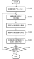
- FIG. 2 is a diagram showing an inspection flow of the appearance inspection method according to this embodiment.
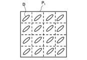
- 3A and 3B are diagrams illustrating a method for creating an inspection image in this embodiment.
- FIG. 4 is a diagram showing an example of pass/fail determination of an inspection image.
- FIG. 5 is a diagram showing an example of pass/fail determination of an inspection image.
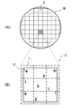
- 6A and 6B are diagrams illustrating a method for inspecting a pattern formed on a semiconductor wafer.
- 7A and 7B are diagrams for explaining a conventional method for creating an inspection image.
- 8A and 8B are diagrams illustrating a conventional process for creating an inspection image.
- FIG. 6 illustrates a method for inspecting a pattern formed on a semiconductor wafer W. As shown in FIG. 6(A), a plurality of chips C on which the same pattern is formed are formed on the semiconductor wafer W.
- the alignment mark M i is usually registered as a unique pattern within each field of view F i .
- FIG. 7A and 7B are diagrams for explaining a method for creating an inspection image.
- a reference image P S of a predetermined range is registered in advance based on the position (x, y) of the alignment mark M i .
- the reference image P S is compared with the inspection image in order to detect defects, and is usually an image selected as a representative image from multiple good product images, or an image generated by a good product learning method.
- FIG. 7B is a diagram showing a state in which the position of the captured field of view F'i is shifted due to the positioning accuracy of the imaging means.
- an inspection image Pt is cut out from the captured image of the field of view F'i based on the imaging position (x', y') of the alignment mark Mi , and the cut-out inspection image Pt is compared with the reference image Ps . This makes it possible to perform an inspection by comparing the inspection image Pt with the reference image Ps at the correct position.
- FIG. 8 is a diagram illustrating a process of relatively scanning the imaging means in the direction of the arrow S to sequentially image the divided fields of view F 1 to F 3 and generate an inspection image Pt .
- alignment marks M1 to M3 are preregistered in the fields of view F1 to F3 , respectively.
- the alignment marks M1 to M3 are unique patterns that are easily recognizable from the patterns in each of the fields of view F1 to F3 .
- the alignment mark M1 is searched for, and an inspection image Pt in the visual field F1 is created based on the imaging position of the recognized alignment mark M1 .
- the alignment marks M2 to M3 are searched for, and an inspection image Pt in the visual fields F2 to F3 is created based on the imaging positions of the recognized alignment marks M2 to M3 .
- the pattern shape of the pattern formed on the object to be inspected may change due to process fluctuations. For example, as shown in FIG. 8B, if a foreign substance adheres to the alignment mark M2 in the field of view F2 , the pattern shape of the alignment mark M2 will be different from the registered pattern shape of the alignment mark M2, and therefore the alignment mark M2 cannot be recognized. Similarly, if the pattern shape of the alignment mark M3 in the field of view F3 changes (in the example shown in FIG. 8B, the linear pattern is thick), the pattern shape of the alignment mark M3 will be different from the registered pattern shape of the alignment mark M3, and therefore the alignment mark M3 cannot be recognized. Therefore, the inspection image Pt cannot be cut out at the correct position, and the inspection by comparing the inspection image Pt with the reference image Ps cannot be performed accurately.
- the present invention is devised to solve such problems, and provides an appearance inspection method and an appearance inspection device that are capable of accurately performing inspection by comparing an inspection image Pt with a reference image PS .
- FIG. 1 is a schematic diagram showing the configuration of an appearance inspection device 100 according to one embodiment of the present invention.
- the inspection image Pt created in the visual field F1 is compared with a reference image Ps registered in advance in the visual field F1 to determine whether the inspection image Pt is good or bad (step S104).
- the quality of the inspection image Pt is determined, for example, by comparing the inspection image Pt with the reference image Ps , and if the difference in the luminance value of each pixel is within a preset range, it is determined to be a good pattern, and if it is outside the range, it is determined to be a bad pattern.
- the divided fields of view F1 to F3 have overlapping regions V1 and V2 in adjacent fields of view ( F1 and F2 ; F2 and F3 ), respectively.
- the overlapping regions V1 and V2 do not necessarily have to be of the same size.
- an inspection image Pt is created, and an image of a predetermined pattern in an overlap region V1 with the adjacent visual field F2 is registered in the storage means 14 as an alignment mark M2 to be used in the adjacent visual field F2 .
- a pattern in a preset position and range in the overlap region V1 is used as the pattern of the alignment mark M2 .
- the position and range of the pattern are registered in the storage means 14 in advance.
- the alignment mark M2 registered within the overlap region V1 with the field of view F1 is searched for, and an inspection image Pt is created based on the imaging position of the recognized alignment mark M2 , and an imaging image of a specified pattern within the overlap region V2 with the adjacent field of view F3 is registered in the memory means 14 as the alignment mark M3 to be used in the adjacent field of view F3 .
- the registered alignment mark M3 is searched for within the overlapping area V2 with the visual field F2 , and an inspection image Pt is created based on the imaging position of the recognized alignment mark M3 .
- process variations may cause changes in the shape of the pattern formed on the inspection object W.
- a foreign substance may adhere to the alignment mark M2 in the field of view F2 , or the pattern shape of the alignment mark M3 in the field of view F3 may change.
- the chips C formed on the semiconductor wafer are divided into a plurality of fields of view, and the inspection image Pt is compared with the reference image Ps for each divided field of view F i to determine whether the inspection image Pt is good or bad.
- the area may be divided into a plurality of fields of view, and the inspection image Pt may be compared with the reference image Ps for each divided field of view F i to determine whether the inspection image Pt is good or bad.
Landscapes
- General Health & Medical Sciences (AREA)
- Health & Medical Sciences (AREA)
- Life Sciences & Earth Sciences (AREA)
- Chemical & Material Sciences (AREA)
- Analytical Chemistry (AREA)
- Biochemistry (AREA)
- Physics & Mathematics (AREA)
- General Physics & Mathematics (AREA)
- Immunology (AREA)
- Pathology (AREA)
- Investigating Materials By The Use Of Optical Means Adapted For Particular Applications (AREA)
- Testing Or Measuring Of Semiconductors Or The Like (AREA)
- Image Processing (AREA)
Abstract
Description
11 撮像手段
12 検査画像作成手段
13 判定手段
14 記憶手段
100 外観検査装置
Fi 視野
Mi アライメントマークPS 基準画像Pt 検査画像
Vi オーバーラップ領域
Claims (6)
- 被検査物を撮像して得られた検査画像に基づいて、前記被検査物の外観を検査する外観検査方法であって、
前記被検査物を、複数の視野に分割して、前記視野毎に順次撮像するステップと、
前記視野毎に撮像された前記被検査物の撮像画像から、前記視野内に設定されたアライメントマークの撮像位置を基準に、前記視野毎に所定範囲の検査画像を作成するステップと、
前記視野毎に作成された前記検査画像の所定領域に対して、該検査画像の良否を判定するステップとを含み、
前記分割された視野は、隣合う視野においてオーバーラップ領域を有し、
前記検査画像を作成するステップでは、前記オーバーラップ領域内にある所定のパターンの撮像画像を、隣の視野で用いられるアライメントマークとして登録し、前記隣の視野で実行される前記検査画像を作成するステップでは、前記登録したアライメントマークの撮像位置を基準に、前記検査画像を作成する、外観検査方法。 - 前記検査画像の良否を判定するステップは、前記視野毎に作成された前記検査画像と、前記視野毎に予め登録された前記所定範囲の基準画像とを比較して、前記検査画像の良否を判定する、請求項1に記載の外観検査方法。
- 前記検査画像を作成するステップにおいて、前記オーバーラップ領域内にある所定のパターンは、前記オーバーラップ領域内の予め設定された位置及び範囲にあるパターンが用いられる、請求項1に記載の外観検査方法。
- 最初に撮像される視野で実行される前記検査画像を作成するステップでは、該視野内にある予め登録されたアライメントマークの撮像位置を基準に、前記検査画像を作成する、請求項1に記載の外観検査方法。
- 被検査物を撮像して得られた検査画像と基準画像に基づいて、前記被検査物の外観を検する外観検査装置であって、
前記被検査物を、複数の視野に分割して、視野毎に順次撮像する撮像手段と、
前記視野毎に撮像された前記被検査物の撮像画像から、前記視野内に設定されたアライメントマークの撮像位置を基準に、前記視野毎に所定範囲の検査画像を作成する検査画像作成手段と、
前記視野毎に作成された前記検査画像に基づいて、該検査画像の良否を判定する判定手段とを備え、
前記分割された視野は、隣合う視野においてオーバーラップ領域を有し、
前記検査画像作成手段では、前記オーバーラップ領域内にある所定のパターンの撮像画像を、隣の視野におけるアライメントマークとして登録し、前記隣の視野で実行される前記検査画像作成手段では、前記登録したアライメントマークの撮像位置を基準に、前記検査画像を作成する、外観検査装置。 - 前記判定手段では、前記視野毎に作成された前記検査画像と、前記視野毎に予め登録された前記所定範囲の基準画像とを比較して、前記検査画像の良否を判定する、請求項5に記載の外観検査装置。
Priority Applications (1)
| Application Number | Priority Date | Filing Date | Title |
|---|---|---|---|
| CN202480008541.0A CN120569624A (zh) | 2023-02-07 | 2024-01-15 | 外观检查方法及外观检查装置 |
Applications Claiming Priority (2)
| Application Number | Priority Date | Filing Date | Title |
|---|---|---|---|
| JP2023016946A JP2024112094A (ja) | 2023-02-07 | 2023-02-07 | 外観検査方法及び外観検査装置 |
| JP2023-016946 | 2023-02-07 |
Publications (1)
| Publication Number | Publication Date |
|---|---|
| WO2024166608A1 true WO2024166608A1 (ja) | 2024-08-15 |
Family
ID=92262321
Family Applications (1)
| Application Number | Title | Priority Date | Filing Date |
|---|---|---|---|
| PCT/JP2024/000736 Ceased WO2024166608A1 (ja) | 2023-02-07 | 2024-01-15 | 外観検査方法及び外観検査装置 |
Country Status (4)
| Country | Link |
|---|---|
| JP (1) | JP2024112094A (ja) |
| CN (1) | CN120569624A (ja) |
| TW (1) | TW202433048A (ja) |
| WO (1) | WO2024166608A1 (ja) |
Citations (5)
| Publication number | Priority date | Publication date | Assignee | Title |
|---|---|---|---|---|
| JP2001202520A (ja) * | 2000-01-24 | 2001-07-27 | Nippon Avionics Co Ltd | パターンの合成方法 |
| JP2007292606A (ja) * | 2006-04-25 | 2007-11-08 | Olympus Corp | 表面検査装置 |
| JP2009157543A (ja) * | 2007-12-26 | 2009-07-16 | Hitachi High-Technologies Corp | 画像生成方法及びその画像生成装置 |
| JP2012517022A (ja) * | 2009-02-04 | 2012-07-26 | 株式会社アドバンテスト | マスク検査装置及び画像生成方法 |
| JP2014137289A (ja) * | 2013-01-17 | 2014-07-28 | Nuflare Technology Inc | 検査方法 |
-
2023
- 2023-02-07 JP JP2023016946A patent/JP2024112094A/ja active Pending
-
2024
- 2024-01-15 WO PCT/JP2024/000736 patent/WO2024166608A1/ja not_active Ceased
- 2024-01-15 CN CN202480008541.0A patent/CN120569624A/zh active Pending
- 2024-01-29 TW TW113103291A patent/TW202433048A/zh unknown
Patent Citations (5)
| Publication number | Priority date | Publication date | Assignee | Title |
|---|---|---|---|---|
| JP2001202520A (ja) * | 2000-01-24 | 2001-07-27 | Nippon Avionics Co Ltd | パターンの合成方法 |
| JP2007292606A (ja) * | 2006-04-25 | 2007-11-08 | Olympus Corp | 表面検査装置 |
| JP2009157543A (ja) * | 2007-12-26 | 2009-07-16 | Hitachi High-Technologies Corp | 画像生成方法及びその画像生成装置 |
| JP2012517022A (ja) * | 2009-02-04 | 2012-07-26 | 株式会社アドバンテスト | マスク検査装置及び画像生成方法 |
| JP2014137289A (ja) * | 2013-01-17 | 2014-07-28 | Nuflare Technology Inc | 検査方法 |
Also Published As
| Publication number | Publication date |
|---|---|
| CN120569624A (zh) | 2025-08-29 |
| TW202433048A (zh) | 2024-08-16 |
| JP2024112094A (ja) | 2024-08-20 |
Similar Documents
| Publication | Publication Date | Title |
|---|---|---|
| US7869643B2 (en) | Advanced cell-to-cell inspection | |
| CN113454445A (zh) | 零件检查期间对于参考未对准进行补偿 | |
| JPH0835936A (ja) | プリント回路基板の自動光学検査装置における歪み補正方法及び装置 | |
| JP5202110B2 (ja) | パターン形状評価方法,パターン形状評価装置,パターン形状評価データ生成装置およびそれを用いた半導体形状評価システム | |
| TWI726977B (zh) | 缺陷檢查裝置 | |
| US7466854B2 (en) | Size checking method and apparatus | |
| KR960013357B1 (ko) | 화상데이타 검사방법 및 장치 | |
| JP4230880B2 (ja) | 欠陥検査方法 | |
| US20140205180A1 (en) | Method, apparatus and device for inspecting circuit pattern defect | |
| JP2004212221A (ja) | パターン検査方法及びパターン検査装置 | |
| JP3907874B2 (ja) | 欠陥検査方法 | |
| US8094926B2 (en) | Ultrafine pattern discrimination using transmitted/reflected workpiece images for use in lithography inspection system | |
| US6965687B2 (en) | Size checking method and apparatus | |
| JP2006252563A (ja) | 画像内の欠陥を検出する方法 | |
| JPS61212708A (ja) | 多層パターン欠陥検出方法及びその装置 | |
| JP2002005850A (ja) | 欠陥検査方法及びその装置、マスクの製造方法 | |
| US8055056B2 (en) | Method of detecting defects of patterns on a semiconductor substrate and apparatus for performing the same | |
| WO2024166608A1 (ja) | 外観検査方法及び外観検査装置 | |
| JP2009294123A (ja) | パターン識別装置、パターン識別方法及び試料検査装置 | |
| JP2007163259A (ja) | 差分比較検査方法および差分比較検査装置 | |
| JP4546607B2 (ja) | 良品パターン登録方法及びパターン検査方法 | |
| JP4428112B2 (ja) | 外観検査方法及び外観検査装置 | |
| JP2002303588A (ja) | パターン欠陥検査装置 | |
| JP3201396B2 (ja) | 半導体デバイスの製造方法 | |
| JPS58179343A (ja) | 図形検査方法 |
Legal Events
| Date | Code | Title | Description |
|---|---|---|---|
| 121 | Ep: the epo has been informed by wipo that ep was designated in this application |
Ref document number: 24753054 Country of ref document: EP Kind code of ref document: A1 |
|
| WWE | Wipo information: entry into national phase |
Ref document number: 202480008541.0 Country of ref document: CN |
|
| WWP | Wipo information: published in national office |
Ref document number: 202480008541.0 Country of ref document: CN |
|
| NENP | Non-entry into the national phase |
Ref country code: DE |
|
| 122 | Ep: pct application non-entry in european phase |
Ref document number: 24753054 Country of ref document: EP Kind code of ref document: A1 |