WO2024166360A1 - Système de calcul quantique et procédé de fabrication de dispositif quantique - Google Patents
Système de calcul quantique et procédé de fabrication de dispositif quantique Download PDFInfo
- Publication number
- WO2024166360A1 WO2024166360A1 PCT/JP2023/004561 JP2023004561W WO2024166360A1 WO 2024166360 A1 WO2024166360 A1 WO 2024166360A1 JP 2023004561 W JP2023004561 W JP 2023004561W WO 2024166360 A1 WO2024166360 A1 WO 2024166360A1
- Authority
- WO
- WIPO (PCT)
- Prior art keywords
- qubit
- magnetic flux
- flux
- quantum
- coupling
- Prior art date
- Legal status (The legal status is an assumption and is not a legal conclusion. Google has not performed a legal analysis and makes no representation as to the accuracy of the status listed.)
- Ceased
Links
Images


Classifications
-
- G—PHYSICS
- G06—COMPUTING OR CALCULATING; COUNTING
- G06N—COMPUTING ARRANGEMENTS BASED ON SPECIFIC COMPUTATIONAL MODELS
- G06N10/00—Quantum computing, i.e. information processing based on quantum-mechanical phenomena
- G06N10/40—Physical realisations or architectures of quantum processors or components for manipulating qubits, e.g. qubit coupling or qubit control
-
- H—ELECTRICITY
- H10—SEMICONDUCTOR DEVICES; ELECTRIC SOLID-STATE DEVICES NOT OTHERWISE PROVIDED FOR
- H10N—ELECTRIC SOLID-STATE DEVICES NOT OTHERWISE PROVIDED FOR
- H10N60/00—Superconducting devices
- H10N60/10—Junction-based devices
- H10N60/12—Josephson-effect devices
-
- B—PERFORMING OPERATIONS; TRANSPORTING
- B82—NANOTECHNOLOGY
- B82Y—SPECIFIC USES OR APPLICATIONS OF NANOSTRUCTURES; MEASUREMENT OR ANALYSIS OF NANOSTRUCTURES; MANUFACTURE OR TREATMENT OF NANOSTRUCTURES
- B82Y10/00—Nanotechnology for information processing, storage or transmission, e.g. quantum computing or single electron logic
Definitions
- This disclosure relates to a quantum computing system and a method for controlling a quantum device.
- quantum computing systems have been proposed that can couple two flux qubits using flux qubits.
- the objective of this disclosure is to provide a quantum computing system and a method for controlling a quantum device that can turn off the coupling between two quantum bits.
- a quantum computing system comprising a quantum device and a control unit that controls the quantum device, the quantum device comprising a first quantum bit, a second quantum bit, a coupling flux qubit that can be coupled to the first quantum bit and the second quantum bit, and a first flux application unit that applies a magnetic flux to the coupling flux qubit, and the control unit causes the first flux application unit to apply a first magnetic flux having a first time modulation in a first period, and to apply a second magnetic flux having a second time modulation different from the first time modulation in a second period different from the first period.
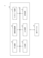
- FIG. 1 is a block diagram showing a quantum computing system according to the first embodiment.
- FIG. 2 is a circuit diagram showing the quantum device according to the first embodiment.
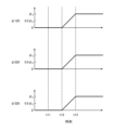
- FIG. 3 is a timing chart showing the change over time of the magnetic flux applied to the SQUID in the first period.
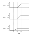
- FIG. 4 is a timing chart showing the change over time of the magnetic flux applied to the SQUID in the second period.
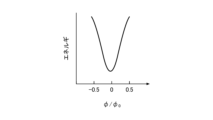
- FIG. 5 is a diagram (part 1) showing the energy state of a flux qubit.
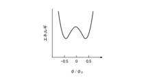
- FIG. 6 is a diagram (part 2) showing the energy state of a flux qubit.
- FIG. 7 is a diagram (part 1) showing the results of the first simulation.
- FIG. 8 is a diagram (part 2) showing the results of the first simulation.
- FIG. 1 is a block diagram showing a quantum computing system according to the first embodiment.
- FIG. 2 is a circuit diagram showing the quantum device according to the first embodiment.
- FIG. 3 is a timing chart showing the change over time of the magnetic flux applied to the SQUID in
- FIG. 9 is a timing chart (part 1) showing the change over time of the magnetic flux applied to the SQUID in the second period in the second simulation.
- FIG. 10 is a timing chart (part 2) showing the change over time of the magnetic flux applied to the SQUID in the second period in the second simulation.
- FIG. 11 is a timing chart (part 3) showing the change over time of the magnetic flux applied to the SQUID in the second period in the second simulation.
- FIG. 12 is a timing chart (part 4) showing the change over time of the magnetic flux applied to the SQUID in the second period in the second simulation.
- FIG. 13 is a diagram (part 1) showing the results of the second simulation.
- FIG. 14 is a diagram (part 2) showing the results of the second simulation.
- FIG. 13 is a diagram (part 1) showing the results of the second simulation.
- FIG. 15 is a diagram (part 1) showing the results of the third simulation.
- FIG. 16 is a diagram (part 2) showing the results of the third simulation.
- FIG. 17 is a block diagram showing a quantum computing system according to the second embodiment.
- FIG. 18 is a circuit diagram showing a quantum device according to the second embodiment.
- FIG. 19 is a timing chart showing the change over time of the current generated by the current source and the magnetic flux applied to the SQUID in the first period.
- FIG. 20 is a timing chart showing the change over time of the current generated by the current source and the magnetic flux applied to the SQUID in the second period.
- FIG. 21 is a diagram showing the relationship between the magnetic flux of a coupling flux qubit and the internal current of a coupled charge qubit.
- FIG. 22 is a plan view showing a first example of the configuration of a quantum device according to the second embodiment.
- FIG. 23 is a cross-sectional view showing a first example of the configuration of a quantum device according to the second embodiment.
- FIG. 24 is a cross-sectional view showing a part of the quantum bit substrate in the second embodiment.
- FIG. 25 is a cross-sectional view showing a portion of another quantum bit substrate according to the second embodiment.
- FIG. 26 is a plan view showing a second example of the configuration of the quantum device according to the second embodiment.
- FIG. 27 is a cross-sectional view showing a second example of the configuration of the quantum device according to the second embodiment.
- FIG. 28 is a plan view showing a third example of the configuration of the quantum device according to the second embodiment.
- Fig. 1 is a block diagram showing a quantum computing system according to the first embodiment.
- the quantum computing system 1 includes a control unit 10 and a quantum device 21.
- the control unit 10 controls the quantum device 21.
- the control unit 10 is a computer and includes a bus 11, an input device 12, an output device 13, a storage device 14, a memory device 15, a processing unit 16, and an interface device 17.
- the input device 12, the output device 13, the storage device 14, the memory device 15, the processing unit 16, and the interface device 17 are connected to the bus 11.
- the input device 12, the output device 13, the storage device 14, the memory device 15, the processing unit 16, and the interface device 17 are connected to each other via the bus 11.
- the input device 12 is a device for inputting various types of information and is realized, for example, by a keyboard or a pointing device.
- the output device 13 is for outputting various types of information and is realized, for example, by a display.
- the interface device 17 includes a LAN card and is used for connecting to a network.
- the storage device 14 stores a control program for controlling the quantum device 21.
- the memory device 15 reads and stores the control program from the storage device 14 when the quantum computing system 1 is started.
- the computing device 16 then performs various processes, as described below, in accordance with the control program stored in the memory device 15.
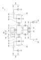
- FIG. 2 is a circuit diagram showing quantum device 21.
- Quantum device 21 has flux qubit 100, flux qubit 200, and coupling flux qubit 300.
- Coupling flux qubit 300 is capable of inductive coupling with flux qubits 100 and 200.
- An example of inductive coupling between flux qubit 100 and flux qubit 200 is disclosed here, but the form of coupling may also be capacitive coupling, or may include inductive coupling and capacitive coupling.
- Quantum device 21 further has flux application units 130, 140, 230, 240, 330, and 340.
- the flux qubit 100 includes a main loop 110 and a superconducting quantum interference device (SQUID) 120.
- the SQUID 120 includes a Josephson junction element 121, a Josephson junction element 122, an inductor 123, and an inductor 124, which are connected in a ring shape and in series in this order.
- the main loop 110 includes inductors 112 and 113, which are connected in series with each other. The end of the inductor 112 opposite the inductor 113 is connected between the Josephson junction element 121 and the Josephson junction element 122. The end of the inductor 113 opposite the inductor 112 is connected between the inductor 123 and the inductor 124.
- the flux qubit 100 includes niobium as a superconducting material.
- the flux qubit 100 is an example of a first qubit and a first flux qubit.
- Flux qubit 200 has main loop 210 and SQUID 220.
- SQUID 220 has Josephson junction element 221, Josephson junction element 222, inductor 223, and inductor 224 connected in a ring shape and in series, in that order.
- Main loop 210 has inductors 212 and 213 connected in series to each other. The end of inductor 213 opposite inductor 212 is connected between Josephson junction element 221 and Josephson junction element 222. The end of inductor 212 opposite inductor 213 is connected between inductor 223 and inductor 224.
- flux qubit 200 contains niobium as a superconducting material. Flux qubit 200 is an example of a second qubit and a second flux qubit.
- the coupling flux qubit 300 has a main loop 310 and a SQUID 320.
- the SQUID 320 has a Josephson junction element 321, a Josephson junction element 322, an inductor 323, and an inductor 324 connected in series in the stated order.
- the main loop 310 has inductors 311, 313, and 312 connected in series in the stated order.
- the end of the inductor 312 opposite to the inductor 313 is connected between the Josephson junction element 321 and the Josephson junction element 322.
- the end of the inductor 311 opposite to the inductor 313 is connected between the inductor 323 and the inductor 324.
- the inductors 311 and 112 are inductively coupled to each other, and the inductors 312 and 212 are inductively coupled to each other.
- the magnetic flux application unit 130 has inductors 131 and 132, and a pulse signal generator 133.
- Inductors 131 and 132 are connected in series with each other. The end of inductor 132 opposite inductor 131 is grounded.
- the pulse signal generator 133 is connected between the end of inductor 131 opposite inductor 132 and ground.
- Inductors 131 and 123 are inductively coupled to each other.
- Inductors 132 and 124 are inductively coupled to each other.
- the magnetic flux application unit 130 is an example of a second magnetic flux application unit.
- the magnetic flux application unit 230 has inductors 231 and 232, and a pulse signal generator 233. Inductors 231 and 232 are connected in series with each other. The end of inductor 231 opposite inductor 232 is grounded. The pulse signal generator 233 is connected between the end of inductor 232 opposite inductor 231 and ground. Inductor 231 and inductor 223 are inductively coupled to each other. Inductor 232 and inductor 224 are inductively coupled to each other.
- the magnetic flux application unit 230 is an example of a third magnetic flux application unit.
- the magnetic flux application unit 330 has inductors 331 and 332, and a pulse signal generator 333.
- Inductors 331 and 332 are connected in series with each other. The end of inductor 332 opposite inductor 331 is grounded.
- the pulse signal generator 333 is connected between the end of inductor 331 opposite inductor 332 and ground.
- Inductors 331 and 323 are inductively coupled to each other.
- Inductors 332 and 324 are inductively coupled to each other.
- the magnetic flux application unit 330 is an example of a first magnetic flux application unit.
- the magnetic flux application unit 140 has an inductor 141 and a DC power supply 142.
- the positive electrodes of the inductor 141 and the DC power supply 142 are connected to each other.
- the end of the inductor 141 opposite the DC power supply 142 is grounded.
- the negative electrode of the DC power supply 142 is grounded.
- the inductor 141 and the inductor 113 are inductively coupled to each other.
- the main loop 310 is an example of a circular wiring.
- the magnetic flux application unit 240 has an inductor 241 and a DC power supply 242.
- the positive electrodes of the inductor 241 and the DC power supply 242 are connected to each other.
- the end of the inductor 241 opposite the DC power supply 242 is grounded.
- the negative electrode of the DC power supply 242 is grounded.
- the inductor 241 and the inductor 213 are inductively coupled to each other.
- the magnetic flux application unit 340 has an inductor 341 and a DC power supply 342.
- the positive electrodes of the inductor 341 and the DC power supply 342 are connected to each other.
- the end of the inductor 341 opposite the DC power supply 342 is grounded.
- the negative electrode of the DC power supply 342 is grounded.
- the inductor 341 and the inductor 313 are inductively coupled to each other.
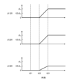
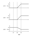
- FIG. 3 is a timing chart showing the time change of the magnetic flux applied to the SQUIDs 120, 220, and 320 in the first period.
- FIG. 4 is a timing chart showing the time change of the magnetic flux applied to the SQUIDs 120, 220, and 320 in the second period.
- FIGS. 5 and 6 are diagrams showing the energy states of the flux qubits. In FIGS.
- ⁇ 120 indicates the magnetic flux applied to the SQUID 120
- ⁇ 220 indicates the magnetic flux applied to the SQUID 220
- ⁇ 320 indicates the magnetic flux applied to the SQUID 320.
- ⁇ 0 is a magnetic flux quantum.
- the horizontal axis in FIGS. 5 and 6 indicates the magnetic flux applied to the main loop.
- FIG. 2 shows some inductors, such as inductors 123 and 124, as separate inductors, an inductor formed as an integral unit may also be used.
- some DC power sources such as DC power source 142
- DC power source 142 are merely examples of power sources, and other forms of power sources, such as arbitrary waveform sources, may also be used.
- the coupling between flux qubit 200 and coupling flux qubit 300 is indirect, and may be inductive, capacitive, or some other type of coupling.
- both the magnetic fluxes ⁇ 120 and ⁇ 220 are 0 (Wb) until time t22, rise to ⁇ 0 from time t22 to time t23, and become ⁇ 0 from time t23.
- the magnetic flux ⁇ 320 is 0 (Wb) until time t21 before time t22, rises to 0.5 ⁇ 0 from time t21 to time t22, and becomes 0.5 ⁇ 0 from time t22.
- the magnetic flux ⁇ 320 may be controlled to become 0.5 ⁇ 0 before time t22.
- the energy value of the ground state when there is one energy ground state is low.
- the energy value of the ground state when there are two energy ground states is higher than the state in FIG. 5.
- the magnetic fluxes ⁇ 120, ⁇ 220, and ⁇ 320 are simultaneously 0.5 ⁇ 0 , and when the magnetic fluxes ⁇ 120, ⁇ 220, and ⁇ 320 are 0.5 ⁇ 0 , the flux qubits 100 and 200 are in a superposition state.
- the magnetic fluxes ⁇ 120, ⁇ 220, and ⁇ 320 subsequently rise to ⁇ 0 , the flux qubits 100 and 200 are in a classical state and the solution converges. Therefore, in the first period, the coupling between the flux qubits 100 and 200 is in an on state.
- flux qubit 100 was controlled to be in a state in which it was likely to be in the "1" state by flux application unit 140, and two types of bias were applied to flux qubit 200 by flux application unit 240. With one bias, the probability of flux qubit 200 being in the "1" state was set to 50%, and with the other bias, flux qubit 200 was made to be likely to be in the "0" state. Then, the above-mentioned first and second periods were controlled. For reference, fluxes ⁇ 120 and ⁇ 220 were changed in the same manner as in the first period, assuming that coupling flux qubit 300 was not present.
- FIGS. 9 to 12 are timing charts showing the time change of the magnetic flux applied to the SQUIDs 120, 220, and 320 in the second period in the second simulation.
- the time change of the magnetic flux applied to the SQUIDs 120 and 220 is the same as the control pattern C shown in FIG. 4.
- control pattern A shown in Figure 9 the magnetic flux ⁇ 320 is always set to 0 (Wb).
- the magnetic flux ⁇ 320 is 0 (Wb) until time t22, increased to 0.5 ⁇ 0 from time t22 to time t23, and set to 0.5 ⁇ 0 from time t23.
- the magnetic flux ⁇ 320 is 0 (Wb) until time t21, increased to 0.5 ⁇ 0 from time t21 to time t22, and set to 0.5 ⁇ 0 from time t22.
- the magnetic flux ⁇ 320 is ⁇ 0 until time t22, is decreased to 0.5 ⁇ 0 from time t22 to time t23, and is set to 0.5 ⁇ 0 from time t23.
- the magnetic flux ⁇ 320 is ⁇ 0 until time t22, is decreased to 0 (Wb) from time t22 to time t23, and is kept at 0 (Wb) from time t23.
- control patterns B and C results similar to those obtained when coupling flux qubit 300 is not present and flux ⁇ 120 and ⁇ 220 are changed in the same manner as in the first period are obtained.
- control pattern C is closest to the results obtained when coupling flux qubit 300 is not present.
- Control patterns B and C in which the flux is biased so that the energy potential of coupling flux qubit 300 has one ground state as shown in FIG. 5, are more resistant to sudden flux changes from the outside and more stable than control pattern A, in which the flux is not biased.
- the quantum tunneling effect is reduced during the period between time t22 and time t23 due to the difference in energy potential between flux qubit 100 and flux qubit 200 and coupling flux qubit 300. Therefore, control pattern B and control pattern C make it easier to control off the coupling between flux qubit 100 and flux qubit 200 than control pattern A.
- control pattern C produced results closer to those obtained when coupling flux qubit 300 was not present than control pattern A.
- control pattern C is particularly preferable.
- flux ⁇ 320 it is preferable for flux ⁇ 320 to be 0.4 ⁇ 0 -0.6 ⁇ 0 before fluxes ⁇ 120 and ⁇ 220 reach 0.3 ⁇ 0 .
- the change in magnetic flux may occur over a period of, for example, 0.1 ns to 100 ms, or 1 ⁇ s to 1 ms.
- Fig. 17 is a block diagram showing a quantum processing system according to the second embodiment.
- the quantum computing system 2 has a control unit 10 and a quantum device 21.
- the control unit 10 controls the quantum device 21.
- the configuration of the control unit 10 is the same as that of the first embodiment, except for the contents of the control program.
- FIG. 18 is a circuit diagram showing quantum device 22.
- Quantum device 22 has charge qubit 400, charge qubit 500, and coupling flux qubit 300.
- Coupling flux qubit 300 can be inductively coupled to charge qubits 400 and 500.
- Quantum device 22 further has charge supplies 430 and 530.
- the configuration of coupling flux qubit 300 is similar to that of the first embodiment.
- the charge quantum bit 400 is, for example, a transmon quantum bit, and has a Josephson junction element 401 and a capacitor 402 connected to each other in a ring shape.
- the charge quantum bit 400 further has an inductor 403 electrically connected in parallel to the Josephson junction element 401 and the capacitor 402.
- the inductor 403 and the inductor 311 are inductively coupled to each other.
- One end of the Josephson junction element 401, the capacitor 402, and the inductor 403 are grounded.
- the charge quantum bit 400 contains titanium nitride as a superconducting material.
- the charge quantum bit 400 is an example of a first quantum bit and a first charge quantum bit. Note that it is not essential to ground one end of the Josephson junction element 401, the capacitor 402, and the inductor 403, and even if they are grounded, they may be connected to the ground plane via a capacitance.
- the charge supply unit 430 is connected to the other ends of the Josephson junction element 401, the capacitor 402, and the inductor 403.
- the charge supply unit 430 has a current source 431 and a capacitor 432.
- the capacitor 432 is connected between one end of the current source 431 and the Josephson junction element 401, the capacitor 402, and the inductor 403. The other end of the current source 431 is grounded.
- the charge quantum bit 500 is, for example, a transmon quantum bit, and includes a Josephson junction element 501 and a capacitor 502 connected in a ring shape.
- the charge quantum bit 500 further includes an inductor 503 electrically connected in parallel to the Josephson junction element 501 and the capacitor 502.
- the inductor 503 and the inductor 312 are inductively coupled to each other.
- One end of the Josephson junction element 501, the capacitor 502, and the inductor 503 are grounded.
- the charge quantum bit 500 includes titanium nitride as a superconducting material.
- the charge quantum bit 500 is an example of a second quantum bit and a second charge quantum bit.
- a charge supply unit 530 is connected to the other ends of the Josephson junction element 501, the capacitor 502, and the inductor 503.
- the charge supply unit 530 has a current source 531 and a capacitor 532.
- the capacitor 532 is connected between one end of the current source 531 and the Josephson junction element 501, the capacitor 502, and the inductor 503. The other end of the current source 531 is grounded.
- Control unit 10 turns on the coupling between charge quantum bit 400 and charge quantum bit 500 during the first period, and turns off the coupling between charge quantum bit 400 and charge quantum bit 500 during the second period.
- FIG. 19 is a timing chart showing the time changes in the current generated by current source 431 and current source 531, and the magnetic flux applied to SQUID 320 during the first period.
- FIG. 20 is a timing chart showing the time changes in the current generated by current source 431 and current source 531, and the magnetic flux applied to SQUID 320 during the second period.
- I431 indicates the current generated by current source 431
- I531 indicates the current generated by current source 531
- ⁇ 320 indicates the magnetic flux applied to SQUID 320.
- the period from time t31 to time t32 corresponds to the first period.
- the current source 431 under the control of the control unit 10, the current source 431 generates a current for the gate operation so as to include the time from time t31 to time t32. While the current source 431 generates a current, the gate operation of the charge quantum bit 400 is performed. Under the control of the control unit 10, the magnetic flux ⁇ 320 becomes 0.5 ⁇ 0 from time t30 to time t31.
- the current generated by the current source 531 is always 0 (A).
- the magnetic flux ⁇ 320 is set to 0 (Wb) in the period between time t31 and time t32. In this period, the coupling between the charge quantum bit 400 and the charge quantum bit 500 is in an ON state. Thereafter, from time t32 onwards, the magnetic flux ⁇ 320 is again set to 0.5 ⁇ 0. It is preferable to return the magnetic flux ⁇ 320 to 0.5 ⁇ 0 from time t32 onwards, but the magnetic flux ⁇ 320 may be maintained at 0 (Wb) even after time t32.
- the period from time t31 to time t32 corresponds to the second period.
- the current source 431 under the control of the control unit 10, the current source 431 generates a current for gate operation so as to include the period from time t31 to time t32. While the current source 431 generates a current, the gate operation of the charge quantum bit 400 is performed.
- the magnetic flux ⁇ 320 becomes 0.5 ⁇ 0 during the period from time t31 to time t32 (second period).
- the current generated by the current source 531 is always 0 (A). Note that FIG. 20 shows an example in which the magnetic flux ⁇ 320 is controlled to be 0.5 ⁇ 0 during the period from time t30 to time t31 and the period after time t32.
- coupling flux qubit 300 when the applied magnetic flux is 0 (Wb) or ⁇ 0 , there are two base states as shown in Fig. 6, and when the applied magnetic flux is 0.5 ⁇ 0 , there is one base state as shown in Fig. 5.
- the applied magnetic flux in coupling flux qubit 300 is 0 (Wb) or ⁇ 0
- the coupling can be controlled to the on state
- the applied magnetic flux is 0.5 ⁇ 0
- the coupling can be controlled to the off state.
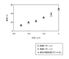
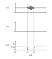
- Figure 21 shows the relationship between the magnetic flux of coupling flux qubit 300 and the internal current of coupled charge qubit 400.
- Figure 21 shows the results of a simulation in which the resonant frequency of charge qubit 400 and charge qubit 500 is 8.1 GHz.
- an excitation signal of 8.1 GHz was applied to charge qubit 500 from current source 531 as a signal source, the internal state of charge qubit 400 was calculated and the internal current Ip was observed.
- the intensity of the signal applied to coupling flux qubit 300 (the output signal of pulse signal generator 333) was modulated.
- FIG. 21 shows a normalized value of the internal current Ip according to the signal strength (magnetic flux applied by the pulse signal generator 333) with reference to the internal current Ip when the signal magnitude is 0. It can be seen that when the magnetic flux is 0 (Wb), the coupling between the charge quantum bit 400 and the charge quantum bit 500 is in the ON state, whereas when the magnetic flux is 0.5 ⁇ 0 , the coupling is in the OFF state.
- Xmon is a flux qubit made of a single-layer wiring, and contains, for example, niobium, titanium nitride, or niobium nitride as a superconducting material.
- the coupling between the coupling flux qubit 300 and the charge qubits 400 and 500 may be capacitive coupling.
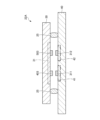
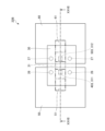
- Fig. 22 is a plan view showing the first example of the configuration of the quantum device 22.
- Fig. 23 is a cross-sectional view showing the first example of the configuration of the quantum device 22.
- Fig. 23 corresponds to a cross-sectional view taken along line XXIII-XXIII in Fig. 22.
- the quantum device 22A of the first example has a quantum bit substrate 30 and a quantum bit substrate 40.
- the quantum bit substrate 30 and the quantum bit substrate 40 are joined to each other via bumps 25.
- the quantum bit substrate 30 is flip-chip bonded to the quantum bit substrate 40.
- the bumps 25 are connected to a ground layer provided on the quantum bit substrate 30 and a ground layer provided on the quantum bit substrate 40.
- the quantum bit substrate 30 includes a coupling flux quantum bit 300, a magnetic flux application unit 330, and a magnetic flux application unit 340.
- the quantum bit substrate 30 has a quantum bit region 31 in which the coupling flux quantum bit 300 is arranged.
- the quantum bit substrate 40 may have wiring or electrodes connected to the flux qubits 100 and 200.
- the quantum bit is not limited to a flux qubit, and may be another quantum bit.
- the quantum bit substrate 40 may have a resonator for observing the state of the quantum bit and an electrode for manipulating the state of the quantum bit.
- a path for introducing a signal for manipulating the state of the quantum bit may be formed by wire bonding from the end of the quantum bit substrate 40, or a through hole may be provided in the quantum bit substrate 40 and a signal may be supplied from the back surface of the quantum bit substrate 40.
- the quantum bit substrate 30 may have a path for supplying a signal at the end or back surface of the quantum bit substrate 30.
- a signal may be supplied from the back surface through the end or through hole of the quantum bit substrate 40 by connecting to a pattern provided on the quantum bit substrate 40 side via a bump.
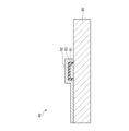
- the quantum bit substrate 30 has, for example, a substrate 80, wiring layers 81, 82, 83, and 84, insulating layers 85, 86, and 87, and a Josephson junction element 88.
- the wiring layer 81 is provided on the substrate 80, and the Josephson junction element 88 is provided on the wiring layer 81.
- the insulating layer 85 is provided on the substrate 80 so as to cover the Josephson junction element 88 and the wiring layer 81.
- the wiring layer 82 is provided on the insulating layer 85 so as to contact the Josephson junction element 88 through an opening formed in the insulating layer 85.
- the insulating layer 86 is provided on the insulating layer 85 so as to cover the wiring layer 82.
- the wiring layer 83 is provided on the insulating layer 86.
- the insulating layer 87 is provided on the insulating layer 86 so as to cover the wiring layer 83.
- the wiring layer 84 is provided on the insulating layer 87 so as to contact the wiring layer 83 through an opening formed in the insulating layer 87.
- the material of the wiring layers 81, 82, 83, and 84 is a material that can become a superconductor, such as niobium or niobium nitride.
- the material of the insulating layers 85, 86, and 87 is, for example, silicon oxide.
- the Josephson junction element 88 has, for example, an aluminum film 88A, an aluminum oxide film 88B, and an aluminum film 88C.
- the aluminum film 88A is connected to the wiring layer 81.
- the aluminum oxide film 88B is provided on the aluminum film 88A.
- the aluminum film 88C is provided on the aluminum oxide film 88B, and the wiring layer 82 is in contact with the aluminum film 88C.
- the Josephson junction element 88 corresponds to the Josephson junction elements 321 and 322.
- the quantum bit substrate 40 includes a charge quantum bit 400, a charge supply unit 430, a charge quantum bit 500, and a charge supply unit 530.
- the quantum bit substrate 40 has a quantum bit region 41 in which the charge quantum bit 400 is arranged, and a quantum bit region 42 in which the charge quantum bit 500 is arranged.
- Figure 25 is a cross-sectional view showing a portion of quantum bit substrate 40.
- Quantum bit substrate 40 has, for example, substrate 90, wiring layers 91 and 92, and insulating layer 93.
- Wiring layer 91 is provided on substrate 90, and insulating layer 93 covers the surface of wiring layer 91.
- Wiring layer 92 is provided on insulating layer 93.
- Wiring layers 91 and 92 and insulating layer 93 form Josephson junction elements corresponding to Josephson junction elements 401, 501.
- Inductor 311 of coupling flux qubit 300 and inductor 403 of charge qubit 400 face each other and are inductively coupled to each other.
- Inductor 312 of coupling flux qubit 300 and inductor 503 of charge qubit 500 face each other and are inductively coupled to each other.
- inductors 311 and 312 of coupling flux quantum bit 300 are connected to wiring layer 84, a part of wiring layer 84 and inductor 403 are inductively coupled to each other, and another part of wiring layer 84 and inductor 503 are inductively coupled to each other.
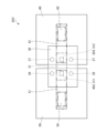
- Fig. 26 is a plan view showing the second example of the configuration of the quantum device 22.
- Fig. 27 is a cross-sectional view showing the second example of the configuration of the quantum device 22.
- Fig. 27 corresponds to a cross-sectional view taken along line XXVII-XXVII in Fig. 26.
- the quantum device 22B of the second example has a quantum bit substrate 30, a quantum bit substrate 50, and a quantum bit substrate 60.
- the quantum bit substrate 30 and the quantum bit substrate 50 are joined to each other via bumps 26, and the quantum bit substrate 30 and the quantum bit substrate 60 are joined to each other via bumps 27.
- the quantum bit substrate 30 is flip-chip bonded to the quantum bit substrates 50 and 60.
- the bumps 26 are connected to a ground layer provided on the quantum bit substrate 30 and a ground layer provided on the quantum bit substrate 50
- the bumps 27 are connected to a ground layer provided on the quantum bit substrate 30 and a ground layer provided on the quantum bit substrate 60.
- the quantum bit substrate 50 includes a charge quantum bit 400 and a charge supply unit 430.
- the quantum bit substrate 50 has a quantum bit region 51 in which the charge quantum bit 400 is arranged.
- the quantum bit substrate 60 includes a charge quantum bit 500 and a charge supply unit 530.
- the quantum bit substrate 60 has a quantum bit region 61 in which the charge quantum bit 500 is arranged.
- Inductor 311 of coupling flux qubit 300 and inductor 403 of charge qubit 400 face each other and are inductively coupled to each other.
- Inductor 312 of coupling flux qubit 300 and inductor 503 of charge qubit 500 face each other and are inductively coupled to each other.
- inductors 311 and 312 of coupling flux quantum bit 300 are connected to wiring layer 84, a portion of wiring layer 83 or 84 is inductively coupled to inductor 403, and another portion of wiring layer 83 or 84 is inductively coupled to inductor 503.
- the quantum bit substrate 50 and the quantum bit substrate 60 may have wiring or electrodes directly or indirectly connected to the quantum bit or the quantum bit.
- the quantum bit substrate 50 and the quantum bit substrate 60 may also have a resonator for observing the state of the quantum bit and an electrode for manipulating the state of the quantum bit.
- a path for introducing a signal for manipulating the state of the quantum bit may be formed by wire bonding from the end of the quantum bit substrate 50 and the quantum bit substrate 60, or a through hole may be provided in the quantum bit substrate 40 and the quantum bit substrate 60 to supply a signal from the back surface of the quantum bit substrate 50 and the quantum bit substrate 60.
- the quantum bit substrate 30 may have a path for supplying a signal at the end or back surface of the quantum bit substrate 30. Also, the signal may be connected to a pattern provided on the quantum bit substrate 50 and the quantum bit substrate 60 side via a bump and supplied from the back surface through the end or through hole of the quantum bit substrate 50 and the quantum bit substrate 60.
- FIG. 28 is a plan view showing the third example of the configuration of the quantum device 22.
- the region 52 of the quantum bit region 51 in which the Josephson junction element 401 and the capacitor 402 are provided is spaced apart from the quantum bit substrate 30 in a planar view. Also, the region 62 of the quantum bit region 61 in which the Josephson junction element 501 and the capacitor 502 are provided is spaced apart from the quantum bit substrate 30 in a planar view.
- the insulating layers 85, 86, and 87 included in the quantum bit substrate 30 can be a source of dielectric loss for the Josephson junction element 401 and the capacitor 402, and for the Josephson junction element 501 and the capacitor 502. In the third example, such dielectric loss can be reduced.
- a ground layer may be provided in the portion of the quantum bit substrate 30 corresponding to the Josephson junction element 401 and the capacitor 402, and the Josephson junction element 501 and the capacitor 502.
- the material of bumps 25, 26, and 27 is preferably a material capable of low-temperature bonding, such as indium or an indium alloy.
- the material of bumps 25, 26, and 27 is preferably a material capable of bonding at 200°C or less, and more preferably a material capable of bonding at 180°C or less.
- the material of bumps 25, 26, and 27 may be a material capable of improving adhesion, such as gold.
- An alloy of indium and gold may also be used. In this case, depending on the composition, it may be capable of bonding at a temperature of 180°C or less and may be a superconducting material.
- the quantum bit substrate 30 and one of the quantum bit substrates 50 and 60 may be connected by a coaxial cable containing a superconducting material (hereinafter, a coaxial cable containing a superconducting material may be referred to as a superconducting cable).
- the superconducting material used in the superconductor cable is, for example, an alloy of niobium and titanium.
- the quantum bit substrate 30 and the quantum bit substrate 50 are joined using bumps 26 as in the second example, and the quantum bit substrate 30 and the quantum bit substrate 60 are coupled by a superconducting cable.
- the inductor 312 of the coupling flux qubit 300 and the superconducting cable are inductively coupled to each other, and the superconducting cable and the inductor 503 of the charge qubit 500 are inductively coupled to each other.
- the quantum bit substrate 30 may be flip-chip bonded to the quantum bit substrate 50.
- the length of the superconducting cable may be several centimeters to several meters, and is typically 1 m to 10 m.
- the coupling state between the charge qubit 400 and the charge qubit 500 can be adjusted by controlling the energy potential of the coupling flux qubit 300.
- the coupling between the superconducting cable and charge qubit 400 or 500 may be capacitive, and the coupling between the superconducting cable and coupling flux qubit 300 may be capacitive.
- a superconducting circuit including a Josephson junction element may also be included in the coupling section, providing direct, inductive, or capacitive coupling.
- the quantum bit substrate 30 and the quantum bit substrate 60 may be joined using bumps 27 as in the second example, and the quantum bit substrate 30 and the quantum bit substrate 50 may be connected by a superconducting cable. Also, the quantum bit substrate 30 and the quantum bit substrates 50 and 60 may be connected by a superconducting cable.
- quantum bit substrates By connecting quantum bit substrates using superconducting cables, it is possible to increase the freedom of arrangement of quantum bit substrates on stages inside the same dilution refrigerator. For example, when placing quantum bit substrates on the lowest temperature stage of a dilution refrigerator, quantum bit substrates can be placed at distant locations and protected by different magnetic shields. In addition, by using long superconducting cables of 5 to 10 meters, quantum bits on quantum bit substrates installed in different dilution refrigerators can be connected to each other.
- the magnetic flux application unit 330 applies a magnetic flux of ⁇ 0 to the coupling flux qubit 300
- an unstable state does not clearly appear in the shape of the energy potential of the coupling flux qubit 300 (see FIG. 6 ).
- the value of the variable ⁇ L expressed by 2 ⁇ LI C / ⁇ 0 is 1.2 to 8.0.
- L is the total inductance of the coupling flux qubit 300
- I C is the sum of the critical current values of the Josephson junction elements 321 and 322. It is more preferable that the value of the variable ⁇ L is 1.2 to 6.0, since an inflection point that is a sign of an unstable state appearing in the energy potential does not clearly appear.
- the critical current value I C of Josephson junction elements 321 and 322 may be 1.0 ⁇ A to 4.0 ⁇ A.
- the smaller the critical current value I C the easier it is to widen the range of selection for the overall inductance L of coupling flux qubit 300.
- the larger the critical current value I C the narrower the range of selection for inductance L, but the easier it is to stably form Josephson junction elements 321 and 322.
- the applied flux is 0.5 ⁇ 0 , but it does not have to be 0.5 ⁇ 0 strictly, and may be 0.4 ⁇ 0 to 0.6 ⁇ 0 .
- the coupling flux quantum bit 300 may have multiple SQUIDs 320 connected in parallel to each other. In this case, the variation in characteristics can be reduced.
- the coupling flux qubit 300 does not have to include the flux application section 340.
- quantum computing system and quantum device disclosed herein can be used, for example, in quantum computing.
- quantum computing system 10 control units 21, 22, 22A, 22B, 22C: quantum devices 30, 40, 50, 60: quantum bit substrates 31, 41, 42, 51, 61: quantum bit regions 100
- 200 flux qubits 110, 210, 310: main loop 120, 220, 320: SQUID 130, 140, 230, 240, 330, 340: magnetic flux application unit 300: coupling flux quantum bit 400, 500: charge quantum bit 430, 530: charge supply unit
Landscapes
- Engineering & Computer Science (AREA)
- General Physics & Mathematics (AREA)
- Theoretical Computer Science (AREA)
- Physics & Mathematics (AREA)
- Mathematical Analysis (AREA)
- Data Mining & Analysis (AREA)
- Evolutionary Computation (AREA)
- Condensed Matter Physics & Semiconductors (AREA)
- Computational Mathematics (AREA)
- Mathematical Optimization (AREA)
- Pure & Applied Mathematics (AREA)
- Computing Systems (AREA)
- General Engineering & Computer Science (AREA)
- Mathematical Physics (AREA)
- Software Systems (AREA)
- Artificial Intelligence (AREA)
- Superconductor Devices And Manufacturing Methods Thereof (AREA)
Abstract
Priority Applications (4)
| Application Number | Priority Date | Filing Date | Title |
|---|---|---|---|
| JP2024576046A JPWO2024166360A1 (fr) | 2023-02-10 | 2023-02-10 | |
| EP23921189.9A EP4665130A1 (fr) | 2023-02-10 | 2023-02-10 | Système de calcul quantique et procédé de fabrication de dispositif quantique |
| PCT/JP2023/004561 WO2024166360A1 (fr) | 2023-02-10 | 2023-02-10 | Système de calcul quantique et procédé de fabrication de dispositif quantique |
| US19/285,202 US20250356238A1 (en) | 2023-02-10 | 2025-07-30 | Quantum computation system and quantum device control method |
Applications Claiming Priority (1)
| Application Number | Priority Date | Filing Date | Title |
|---|---|---|---|
| PCT/JP2023/004561 WO2024166360A1 (fr) | 2023-02-10 | 2023-02-10 | Système de calcul quantique et procédé de fabrication de dispositif quantique |
Related Child Applications (1)
| Application Number | Title | Priority Date | Filing Date |
|---|---|---|---|
| US19/285,202 Continuation US20250356238A1 (en) | 2023-02-10 | 2025-07-30 | Quantum computation system and quantum device control method |
Publications (1)
| Publication Number | Publication Date |
|---|---|
| WO2024166360A1 true WO2024166360A1 (fr) | 2024-08-15 |
Family
ID=92262264
Family Applications (1)
| Application Number | Title | Priority Date | Filing Date |
|---|---|---|---|
| PCT/JP2023/004561 Ceased WO2024166360A1 (fr) | 2023-02-10 | 2023-02-10 | Système de calcul quantique et procédé de fabrication de dispositif quantique |
Country Status (4)
| Country | Link |
|---|---|
| US (1) | US20250356238A1 (fr) |
| EP (1) | EP4665130A1 (fr) |
| JP (1) | JPWO2024166360A1 (fr) |
| WO (1) | WO2024166360A1 (fr) |
Citations (6)
| Publication number | Priority date | Publication date | Assignee | Title |
|---|---|---|---|---|
| JP2007214885A (ja) * | 2006-02-09 | 2007-08-23 | Nec Corp | 超伝導量子演算回路 |
| WO2008029815A1 (fr) | 2006-09-05 | 2008-03-13 | Nec Corporation | Procédé de couplage variable de bits quantiques, circuit de calcul quantique utilisant le procédé et coupleur variable |
| JP2014241073A (ja) * | 2013-06-12 | 2014-12-25 | 日本電信電話株式会社 | 量子ビット制御方法 |
| JP2019508876A (ja) | 2015-12-31 | 2019-03-28 | インターナショナル・ビジネス・マシーンズ・コーポレーションInternational Business Machines Corporation | 結合機構、結合機構起動方法、結合機構を含む正方格子および結合機構を含む量子ゲート |
| JP2021511657A (ja) * | 2018-01-11 | 2021-05-06 | ノースロップ グラマン システムズ コーポレーション | 容量駆動の調整可能な結合 |
| JP2022525910A (ja) | 2019-04-02 | 2022-05-20 | インターナショナル・ビジネス・マシーンズ・コーポレーション | 量子コンピューティング・デバイス用の調整可能な超伝導共振器のためのデバイス、方法、システム |
-
2023
- 2023-02-10 WO PCT/JP2023/004561 patent/WO2024166360A1/fr not_active Ceased
- 2023-02-10 JP JP2024576046A patent/JPWO2024166360A1/ja active Pending
- 2023-02-10 EP EP23921189.9A patent/EP4665130A1/fr active Pending
-
2025
- 2025-07-30 US US19/285,202 patent/US20250356238A1/en active Pending
Patent Citations (6)
| Publication number | Priority date | Publication date | Assignee | Title |
|---|---|---|---|---|
| JP2007214885A (ja) * | 2006-02-09 | 2007-08-23 | Nec Corp | 超伝導量子演算回路 |
| WO2008029815A1 (fr) | 2006-09-05 | 2008-03-13 | Nec Corporation | Procédé de couplage variable de bits quantiques, circuit de calcul quantique utilisant le procédé et coupleur variable |
| JP2014241073A (ja) * | 2013-06-12 | 2014-12-25 | 日本電信電話株式会社 | 量子ビット制御方法 |
| JP2019508876A (ja) | 2015-12-31 | 2019-03-28 | インターナショナル・ビジネス・マシーンズ・コーポレーションInternational Business Machines Corporation | 結合機構、結合機構起動方法、結合機構を含む正方格子および結合機構を含む量子ゲート |
| JP2021511657A (ja) * | 2018-01-11 | 2021-05-06 | ノースロップ グラマン システムズ コーポレーション | 容量駆動の調整可能な結合 |
| JP2022525910A (ja) | 2019-04-02 | 2022-05-20 | インターナショナル・ビジネス・マシーンズ・コーポレーション | 量子コンピューティング・デバイス用の調整可能な超伝導共振器のためのデバイス、方法、システム |
Also Published As
| Publication number | Publication date |
|---|---|
| JPWO2024166360A1 (fr) | 2024-08-15 |
| US20250356238A1 (en) | 2025-11-20 |
| EP4665130A1 (fr) | 2025-12-17 |
Similar Documents
| Publication | Publication Date | Title |
|---|---|---|
| US11569205B2 (en) | Reducing loss in stacked quantum devices | |
| JP2023103206A (ja) | 共振器、発振器、及び量子計算機 | |
| AU2020202779B2 (en) | Programmable universal quantum annealing with co-planar waveguide flux qubits | |
| US11133451B2 (en) | Superconducting bump bonds | |
| US10256206B2 (en) | Qubit die attachment using preforms | |
| US11569428B2 (en) | Superconducting qubit device packages | |
| US20230056318A1 (en) | Low footprint resonator in flip chip geometry | |
| US11839164B2 (en) | Systems and methods for addressing devices in a superconducting circuit | |
| JP7765565B2 (ja) | カプラ及び計算装置 | |
| WO2019117883A1 (fr) | Dispositifs à bits quantiques à jonctions josephson fabriquées à l'aide d'un pont aérien ou d'un porte-à-faux | |
| JP7398117B2 (ja) | 高速/低速電力サーバファームおよびサーバネットワーク | |
| US20230142878A1 (en) | Superconducting quantum circuit | |
| US20220318660A1 (en) | Superconducting circuit and quantum computer | |
| US11955931B2 (en) | Power amplifier unit | |
| JP7279792B2 (ja) | 共振器、発振器、及び量子計算機 | |
| WO2024166360A1 (fr) | Système de calcul quantique et procédé de fabrication de dispositif quantique | |
| CN110709934A (zh) | 超导装置中的磁通量控制 | |
| US12490659B2 (en) | Oscillator and quantum computer | |
| JP2024148610A (ja) | 電子回路及び計算装置 | |
| JP2025131195A (ja) | 超伝導量子回路 | |
| JPWO2024166360A5 (fr) |
Legal Events
| Date | Code | Title | Description |
|---|---|---|---|
| 121 | Ep: the epo has been informed by wipo that ep was designated in this application |
Ref document number: 23921189 Country of ref document: EP Kind code of ref document: A1 |
|
| ENP | Entry into the national phase |
Ref document number: 2024576046 Country of ref document: JP Kind code of ref document: A |
|
| WWE | Wipo information: entry into national phase |
Ref document number: 2024576046 Country of ref document: JP |
|
| NENP | Non-entry into the national phase |
Ref country code: DE |
|
| WWP | Wipo information: published in national office |
Ref document number: 2023921189 Country of ref document: EP |