WO2024166360A1 - Quantum computation system and quantum device manufacturing method - Google Patents
Quantum computation system and quantum device manufacturing method Download PDFInfo
- Publication number
- WO2024166360A1 WO2024166360A1 PCT/JP2023/004561 JP2023004561W WO2024166360A1 WO 2024166360 A1 WO2024166360 A1 WO 2024166360A1 JP 2023004561 W JP2023004561 W JP 2023004561W WO 2024166360 A1 WO2024166360 A1 WO 2024166360A1
- Authority
- WO
- WIPO (PCT)
- Prior art keywords
- qubit
- magnetic flux
- flux
- quantum
- coupling
- Prior art date
- Legal status (The legal status is an assumption and is not a legal conclusion. Google has not performed a legal analysis and makes no representation as to the accuracy of the status listed.)
- Ceased
Links
Images


Classifications
-
- G—PHYSICS
- G06—COMPUTING OR CALCULATING; COUNTING
- G06N—COMPUTING ARRANGEMENTS BASED ON SPECIFIC COMPUTATIONAL MODELS
- G06N10/00—Quantum computing, i.e. information processing based on quantum-mechanical phenomena
- G06N10/40—Physical realisations or architectures of quantum processors or components for manipulating qubits, e.g. qubit coupling or qubit control
-
- H—ELECTRICITY
- H10—SEMICONDUCTOR DEVICES; ELECTRIC SOLID-STATE DEVICES NOT OTHERWISE PROVIDED FOR
- H10N—ELECTRIC SOLID-STATE DEVICES NOT OTHERWISE PROVIDED FOR
- H10N60/00—Superconducting devices
- H10N60/10—Junction-based devices
- H10N60/12—Josephson-effect devices
-
- B—PERFORMING OPERATIONS; TRANSPORTING
- B82—NANOTECHNOLOGY
- B82Y—SPECIFIC USES OR APPLICATIONS OF NANOSTRUCTURES; MEASUREMENT OR ANALYSIS OF NANOSTRUCTURES; MANUFACTURE OR TREATMENT OF NANOSTRUCTURES
- B82Y10/00—Nanotechnology for information processing, storage or transmission, e.g. quantum computing or single electron logic
Definitions
- This disclosure relates to a quantum computing system and a method for controlling a quantum device.
- quantum computing systems have been proposed that can couple two flux qubits using flux qubits.
- the objective of this disclosure is to provide a quantum computing system and a method for controlling a quantum device that can turn off the coupling between two quantum bits.
- a quantum computing system comprising a quantum device and a control unit that controls the quantum device, the quantum device comprising a first quantum bit, a second quantum bit, a coupling flux qubit that can be coupled to the first quantum bit and the second quantum bit, and a first flux application unit that applies a magnetic flux to the coupling flux qubit, and the control unit causes the first flux application unit to apply a first magnetic flux having a first time modulation in a first period, and to apply a second magnetic flux having a second time modulation different from the first time modulation in a second period different from the first period.
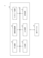
- FIG. 1 is a block diagram showing a quantum computing system according to the first embodiment.
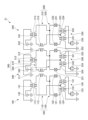
- FIG. 2 is a circuit diagram showing the quantum device according to the first embodiment.
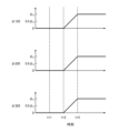
- FIG. 3 is a timing chart showing the change over time of the magnetic flux applied to the SQUID in the first period.
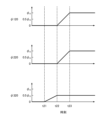
- FIG. 4 is a timing chart showing the change over time of the magnetic flux applied to the SQUID in the second period.
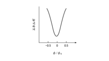
- FIG. 5 is a diagram (part 1) showing the energy state of a flux qubit.
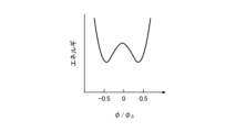
- FIG. 6 is a diagram (part 2) showing the energy state of a flux qubit.
- FIG. 7 is a diagram (part 1) showing the results of the first simulation.
- FIG. 8 is a diagram (part 2) showing the results of the first simulation.
- FIG. 1 is a block diagram showing a quantum computing system according to the first embodiment.
- FIG. 2 is a circuit diagram showing the quantum device according to the first embodiment.
- FIG. 3 is a timing chart showing the change over time of the magnetic flux applied to the SQUID in
- FIG. 9 is a timing chart (part 1) showing the change over time of the magnetic flux applied to the SQUID in the second period in the second simulation.
- FIG. 10 is a timing chart (part 2) showing the change over time of the magnetic flux applied to the SQUID in the second period in the second simulation.
- FIG. 11 is a timing chart (part 3) showing the change over time of the magnetic flux applied to the SQUID in the second period in the second simulation.
- FIG. 12 is a timing chart (part 4) showing the change over time of the magnetic flux applied to the SQUID in the second period in the second simulation.
- FIG. 13 is a diagram (part 1) showing the results of the second simulation.
- FIG. 14 is a diagram (part 2) showing the results of the second simulation.
- FIG. 13 is a diagram (part 1) showing the results of the second simulation.
- FIG. 15 is a diagram (part 1) showing the results of the third simulation.
- FIG. 16 is a diagram (part 2) showing the results of the third simulation.
- FIG. 17 is a block diagram showing a quantum computing system according to the second embodiment.
- FIG. 18 is a circuit diagram showing a quantum device according to the second embodiment.
- FIG. 19 is a timing chart showing the change over time of the current generated by the current source and the magnetic flux applied to the SQUID in the first period.
- FIG. 20 is a timing chart showing the change over time of the current generated by the current source and the magnetic flux applied to the SQUID in the second period.
- FIG. 21 is a diagram showing the relationship between the magnetic flux of a coupling flux qubit and the internal current of a coupled charge qubit.
- FIG. 22 is a plan view showing a first example of the configuration of a quantum device according to the second embodiment.
- FIG. 23 is a cross-sectional view showing a first example of the configuration of a quantum device according to the second embodiment.
- FIG. 24 is a cross-sectional view showing a part of the quantum bit substrate in the second embodiment.
- FIG. 25 is a cross-sectional view showing a portion of another quantum bit substrate according to the second embodiment.
- FIG. 26 is a plan view showing a second example of the configuration of the quantum device according to the second embodiment.
- FIG. 27 is a cross-sectional view showing a second example of the configuration of the quantum device according to the second embodiment.
- FIG. 28 is a plan view showing a third example of the configuration of the quantum device according to the second embodiment.
- Fig. 1 is a block diagram showing a quantum computing system according to the first embodiment.
- the quantum computing system 1 includes a control unit 10 and a quantum device 21.
- the control unit 10 controls the quantum device 21.
- the control unit 10 is a computer and includes a bus 11, an input device 12, an output device 13, a storage device 14, a memory device 15, a processing unit 16, and an interface device 17.
- the input device 12, the output device 13, the storage device 14, the memory device 15, the processing unit 16, and the interface device 17 are connected to the bus 11.
- the input device 12, the output device 13, the storage device 14, the memory device 15, the processing unit 16, and the interface device 17 are connected to each other via the bus 11.
- the input device 12 is a device for inputting various types of information and is realized, for example, by a keyboard or a pointing device.
- the output device 13 is for outputting various types of information and is realized, for example, by a display.
- the interface device 17 includes a LAN card and is used for connecting to a network.
- the storage device 14 stores a control program for controlling the quantum device 21.
- the memory device 15 reads and stores the control program from the storage device 14 when the quantum computing system 1 is started.
- the computing device 16 then performs various processes, as described below, in accordance with the control program stored in the memory device 15.
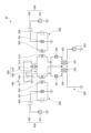
- FIG. 2 is a circuit diagram showing quantum device 21.
- Quantum device 21 has flux qubit 100, flux qubit 200, and coupling flux qubit 300.
- Coupling flux qubit 300 is capable of inductive coupling with flux qubits 100 and 200.
- An example of inductive coupling between flux qubit 100 and flux qubit 200 is disclosed here, but the form of coupling may also be capacitive coupling, or may include inductive coupling and capacitive coupling.
- Quantum device 21 further has flux application units 130, 140, 230, 240, 330, and 340.
- the flux qubit 100 includes a main loop 110 and a superconducting quantum interference device (SQUID) 120.
- the SQUID 120 includes a Josephson junction element 121, a Josephson junction element 122, an inductor 123, and an inductor 124, which are connected in a ring shape and in series in this order.
- the main loop 110 includes inductors 112 and 113, which are connected in series with each other. The end of the inductor 112 opposite the inductor 113 is connected between the Josephson junction element 121 and the Josephson junction element 122. The end of the inductor 113 opposite the inductor 112 is connected between the inductor 123 and the inductor 124.
- the flux qubit 100 includes niobium as a superconducting material.
- the flux qubit 100 is an example of a first qubit and a first flux qubit.
- Flux qubit 200 has main loop 210 and SQUID 220.
- SQUID 220 has Josephson junction element 221, Josephson junction element 222, inductor 223, and inductor 224 connected in a ring shape and in series, in that order.
- Main loop 210 has inductors 212 and 213 connected in series to each other. The end of inductor 213 opposite inductor 212 is connected between Josephson junction element 221 and Josephson junction element 222. The end of inductor 212 opposite inductor 213 is connected between inductor 223 and inductor 224.
- flux qubit 200 contains niobium as a superconducting material. Flux qubit 200 is an example of a second qubit and a second flux qubit.
- the coupling flux qubit 300 has a main loop 310 and a SQUID 320.
- the SQUID 320 has a Josephson junction element 321, a Josephson junction element 322, an inductor 323, and an inductor 324 connected in series in the stated order.
- the main loop 310 has inductors 311, 313, and 312 connected in series in the stated order.
- the end of the inductor 312 opposite to the inductor 313 is connected between the Josephson junction element 321 and the Josephson junction element 322.
- the end of the inductor 311 opposite to the inductor 313 is connected between the inductor 323 and the inductor 324.
- the inductors 311 and 112 are inductively coupled to each other, and the inductors 312 and 212 are inductively coupled to each other.
- the magnetic flux application unit 130 has inductors 131 and 132, and a pulse signal generator 133.
- Inductors 131 and 132 are connected in series with each other. The end of inductor 132 opposite inductor 131 is grounded.
- the pulse signal generator 133 is connected between the end of inductor 131 opposite inductor 132 and ground.
- Inductors 131 and 123 are inductively coupled to each other.
- Inductors 132 and 124 are inductively coupled to each other.
- the magnetic flux application unit 130 is an example of a second magnetic flux application unit.
- the magnetic flux application unit 230 has inductors 231 and 232, and a pulse signal generator 233. Inductors 231 and 232 are connected in series with each other. The end of inductor 231 opposite inductor 232 is grounded. The pulse signal generator 233 is connected between the end of inductor 232 opposite inductor 231 and ground. Inductor 231 and inductor 223 are inductively coupled to each other. Inductor 232 and inductor 224 are inductively coupled to each other.
- the magnetic flux application unit 230 is an example of a third magnetic flux application unit.
- the magnetic flux application unit 330 has inductors 331 and 332, and a pulse signal generator 333.
- Inductors 331 and 332 are connected in series with each other. The end of inductor 332 opposite inductor 331 is grounded.
- the pulse signal generator 333 is connected between the end of inductor 331 opposite inductor 332 and ground.
- Inductors 331 and 323 are inductively coupled to each other.
- Inductors 332 and 324 are inductively coupled to each other.
- the magnetic flux application unit 330 is an example of a first magnetic flux application unit.
- the magnetic flux application unit 140 has an inductor 141 and a DC power supply 142.
- the positive electrodes of the inductor 141 and the DC power supply 142 are connected to each other.
- the end of the inductor 141 opposite the DC power supply 142 is grounded.
- the negative electrode of the DC power supply 142 is grounded.
- the inductor 141 and the inductor 113 are inductively coupled to each other.
- the main loop 310 is an example of a circular wiring.
- the magnetic flux application unit 240 has an inductor 241 and a DC power supply 242.
- the positive electrodes of the inductor 241 and the DC power supply 242 are connected to each other.
- the end of the inductor 241 opposite the DC power supply 242 is grounded.
- the negative electrode of the DC power supply 242 is grounded.
- the inductor 241 and the inductor 213 are inductively coupled to each other.
- the magnetic flux application unit 340 has an inductor 341 and a DC power supply 342.
- the positive electrodes of the inductor 341 and the DC power supply 342 are connected to each other.
- the end of the inductor 341 opposite the DC power supply 342 is grounded.
- the negative electrode of the DC power supply 342 is grounded.
- the inductor 341 and the inductor 313 are inductively coupled to each other.
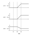
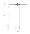
- FIG. 3 is a timing chart showing the time change of the magnetic flux applied to the SQUIDs 120, 220, and 320 in the first period.
- FIG. 4 is a timing chart showing the time change of the magnetic flux applied to the SQUIDs 120, 220, and 320 in the second period.
- FIGS. 5 and 6 are diagrams showing the energy states of the flux qubits. In FIGS.
- ⁇ 120 indicates the magnetic flux applied to the SQUID 120
- ⁇ 220 indicates the magnetic flux applied to the SQUID 220
- ⁇ 320 indicates the magnetic flux applied to the SQUID 320.
- ⁇ 0 is a magnetic flux quantum.
- the horizontal axis in FIGS. 5 and 6 indicates the magnetic flux applied to the main loop.
- FIG. 2 shows some inductors, such as inductors 123 and 124, as separate inductors, an inductor formed as an integral unit may also be used.
- some DC power sources such as DC power source 142
- DC power source 142 are merely examples of power sources, and other forms of power sources, such as arbitrary waveform sources, may also be used.
- the coupling between flux qubit 200 and coupling flux qubit 300 is indirect, and may be inductive, capacitive, or some other type of coupling.
- both the magnetic fluxes ⁇ 120 and ⁇ 220 are 0 (Wb) until time t22, rise to ⁇ 0 from time t22 to time t23, and become ⁇ 0 from time t23.
- the magnetic flux ⁇ 320 is 0 (Wb) until time t21 before time t22, rises to 0.5 ⁇ 0 from time t21 to time t22, and becomes 0.5 ⁇ 0 from time t22.
- the magnetic flux ⁇ 320 may be controlled to become 0.5 ⁇ 0 before time t22.
- the energy value of the ground state when there is one energy ground state is low.
- the energy value of the ground state when there are two energy ground states is higher than the state in FIG. 5.
- the magnetic fluxes ⁇ 120, ⁇ 220, and ⁇ 320 are simultaneously 0.5 ⁇ 0 , and when the magnetic fluxes ⁇ 120, ⁇ 220, and ⁇ 320 are 0.5 ⁇ 0 , the flux qubits 100 and 200 are in a superposition state.
- the magnetic fluxes ⁇ 120, ⁇ 220, and ⁇ 320 subsequently rise to ⁇ 0 , the flux qubits 100 and 200 are in a classical state and the solution converges. Therefore, in the first period, the coupling between the flux qubits 100 and 200 is in an on state.
- flux qubit 100 was controlled to be in a state in which it was likely to be in the "1" state by flux application unit 140, and two types of bias were applied to flux qubit 200 by flux application unit 240. With one bias, the probability of flux qubit 200 being in the "1" state was set to 50%, and with the other bias, flux qubit 200 was made to be likely to be in the "0" state. Then, the above-mentioned first and second periods were controlled. For reference, fluxes ⁇ 120 and ⁇ 220 were changed in the same manner as in the first period, assuming that coupling flux qubit 300 was not present.
- FIGS. 9 to 12 are timing charts showing the time change of the magnetic flux applied to the SQUIDs 120, 220, and 320 in the second period in the second simulation.
- the time change of the magnetic flux applied to the SQUIDs 120 and 220 is the same as the control pattern C shown in FIG. 4.
- control pattern A shown in Figure 9 the magnetic flux ⁇ 320 is always set to 0 (Wb).
- the magnetic flux ⁇ 320 is 0 (Wb) until time t22, increased to 0.5 ⁇ 0 from time t22 to time t23, and set to 0.5 ⁇ 0 from time t23.
- the magnetic flux ⁇ 320 is 0 (Wb) until time t21, increased to 0.5 ⁇ 0 from time t21 to time t22, and set to 0.5 ⁇ 0 from time t22.
- the magnetic flux ⁇ 320 is ⁇ 0 until time t22, is decreased to 0.5 ⁇ 0 from time t22 to time t23, and is set to 0.5 ⁇ 0 from time t23.
- the magnetic flux ⁇ 320 is ⁇ 0 until time t22, is decreased to 0 (Wb) from time t22 to time t23, and is kept at 0 (Wb) from time t23.
- control patterns B and C results similar to those obtained when coupling flux qubit 300 is not present and flux ⁇ 120 and ⁇ 220 are changed in the same manner as in the first period are obtained.
- control pattern C is closest to the results obtained when coupling flux qubit 300 is not present.
- Control patterns B and C in which the flux is biased so that the energy potential of coupling flux qubit 300 has one ground state as shown in FIG. 5, are more resistant to sudden flux changes from the outside and more stable than control pattern A, in which the flux is not biased.
- the quantum tunneling effect is reduced during the period between time t22 and time t23 due to the difference in energy potential between flux qubit 100 and flux qubit 200 and coupling flux qubit 300. Therefore, control pattern B and control pattern C make it easier to control off the coupling between flux qubit 100 and flux qubit 200 than control pattern A.
- control pattern C produced results closer to those obtained when coupling flux qubit 300 was not present than control pattern A.
- control pattern C is particularly preferable.
- flux ⁇ 320 it is preferable for flux ⁇ 320 to be 0.4 ⁇ 0 -0.6 ⁇ 0 before fluxes ⁇ 120 and ⁇ 220 reach 0.3 ⁇ 0 .
- the change in magnetic flux may occur over a period of, for example, 0.1 ns to 100 ms, or 1 ⁇ s to 1 ms.
- Fig. 17 is a block diagram showing a quantum processing system according to the second embodiment.
- the quantum computing system 2 has a control unit 10 and a quantum device 21.
- the control unit 10 controls the quantum device 21.
- the configuration of the control unit 10 is the same as that of the first embodiment, except for the contents of the control program.
- FIG. 18 is a circuit diagram showing quantum device 22.
- Quantum device 22 has charge qubit 400, charge qubit 500, and coupling flux qubit 300.
- Coupling flux qubit 300 can be inductively coupled to charge qubits 400 and 500.
- Quantum device 22 further has charge supplies 430 and 530.
- the configuration of coupling flux qubit 300 is similar to that of the first embodiment.
- the charge quantum bit 400 is, for example, a transmon quantum bit, and has a Josephson junction element 401 and a capacitor 402 connected to each other in a ring shape.
- the charge quantum bit 400 further has an inductor 403 electrically connected in parallel to the Josephson junction element 401 and the capacitor 402.
- the inductor 403 and the inductor 311 are inductively coupled to each other.
- One end of the Josephson junction element 401, the capacitor 402, and the inductor 403 are grounded.
- the charge quantum bit 400 contains titanium nitride as a superconducting material.
- the charge quantum bit 400 is an example of a first quantum bit and a first charge quantum bit. Note that it is not essential to ground one end of the Josephson junction element 401, the capacitor 402, and the inductor 403, and even if they are grounded, they may be connected to the ground plane via a capacitance.
- the charge supply unit 430 is connected to the other ends of the Josephson junction element 401, the capacitor 402, and the inductor 403.
- the charge supply unit 430 has a current source 431 and a capacitor 432.
- the capacitor 432 is connected between one end of the current source 431 and the Josephson junction element 401, the capacitor 402, and the inductor 403. The other end of the current source 431 is grounded.
- the charge quantum bit 500 is, for example, a transmon quantum bit, and includes a Josephson junction element 501 and a capacitor 502 connected in a ring shape.
- the charge quantum bit 500 further includes an inductor 503 electrically connected in parallel to the Josephson junction element 501 and the capacitor 502.
- the inductor 503 and the inductor 312 are inductively coupled to each other.
- One end of the Josephson junction element 501, the capacitor 502, and the inductor 503 are grounded.
- the charge quantum bit 500 includes titanium nitride as a superconducting material.
- the charge quantum bit 500 is an example of a second quantum bit and a second charge quantum bit.
- a charge supply unit 530 is connected to the other ends of the Josephson junction element 501, the capacitor 502, and the inductor 503.
- the charge supply unit 530 has a current source 531 and a capacitor 532.
- the capacitor 532 is connected between one end of the current source 531 and the Josephson junction element 501, the capacitor 502, and the inductor 503. The other end of the current source 531 is grounded.
- Control unit 10 turns on the coupling between charge quantum bit 400 and charge quantum bit 500 during the first period, and turns off the coupling between charge quantum bit 400 and charge quantum bit 500 during the second period.
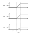
- FIG. 19 is a timing chart showing the time changes in the current generated by current source 431 and current source 531, and the magnetic flux applied to SQUID 320 during the first period.
- FIG. 20 is a timing chart showing the time changes in the current generated by current source 431 and current source 531, and the magnetic flux applied to SQUID 320 during the second period.
- I431 indicates the current generated by current source 431
- I531 indicates the current generated by current source 531
- ⁇ 320 indicates the magnetic flux applied to SQUID 320.
- the period from time t31 to time t32 corresponds to the first period.
- the current source 431 under the control of the control unit 10, the current source 431 generates a current for the gate operation so as to include the time from time t31 to time t32. While the current source 431 generates a current, the gate operation of the charge quantum bit 400 is performed. Under the control of the control unit 10, the magnetic flux ⁇ 320 becomes 0.5 ⁇ 0 from time t30 to time t31.
- the current generated by the current source 531 is always 0 (A).
- the magnetic flux ⁇ 320 is set to 0 (Wb) in the period between time t31 and time t32. In this period, the coupling between the charge quantum bit 400 and the charge quantum bit 500 is in an ON state. Thereafter, from time t32 onwards, the magnetic flux ⁇ 320 is again set to 0.5 ⁇ 0. It is preferable to return the magnetic flux ⁇ 320 to 0.5 ⁇ 0 from time t32 onwards, but the magnetic flux ⁇ 320 may be maintained at 0 (Wb) even after time t32.
- the period from time t31 to time t32 corresponds to the second period.
- the current source 431 under the control of the control unit 10, the current source 431 generates a current for gate operation so as to include the period from time t31 to time t32. While the current source 431 generates a current, the gate operation of the charge quantum bit 400 is performed.
- the magnetic flux ⁇ 320 becomes 0.5 ⁇ 0 during the period from time t31 to time t32 (second period).
- the current generated by the current source 531 is always 0 (A). Note that FIG. 20 shows an example in which the magnetic flux ⁇ 320 is controlled to be 0.5 ⁇ 0 during the period from time t30 to time t31 and the period after time t32.
- coupling flux qubit 300 when the applied magnetic flux is 0 (Wb) or ⁇ 0 , there are two base states as shown in Fig. 6, and when the applied magnetic flux is 0.5 ⁇ 0 , there is one base state as shown in Fig. 5.
- the applied magnetic flux in coupling flux qubit 300 is 0 (Wb) or ⁇ 0
- the coupling can be controlled to the on state
- the applied magnetic flux is 0.5 ⁇ 0
- the coupling can be controlled to the off state.
- Figure 21 shows the relationship between the magnetic flux of coupling flux qubit 300 and the internal current of coupled charge qubit 400.
- Figure 21 shows the results of a simulation in which the resonant frequency of charge qubit 400 and charge qubit 500 is 8.1 GHz.
- an excitation signal of 8.1 GHz was applied to charge qubit 500 from current source 531 as a signal source, the internal state of charge qubit 400 was calculated and the internal current Ip was observed.
- the intensity of the signal applied to coupling flux qubit 300 (the output signal of pulse signal generator 333) was modulated.
- FIG. 21 shows a normalized value of the internal current Ip according to the signal strength (magnetic flux applied by the pulse signal generator 333) with reference to the internal current Ip when the signal magnitude is 0. It can be seen that when the magnetic flux is 0 (Wb), the coupling between the charge quantum bit 400 and the charge quantum bit 500 is in the ON state, whereas when the magnetic flux is 0.5 ⁇ 0 , the coupling is in the OFF state.
- Xmon is a flux qubit made of a single-layer wiring, and contains, for example, niobium, titanium nitride, or niobium nitride as a superconducting material.
- the coupling between the coupling flux qubit 300 and the charge qubits 400 and 500 may be capacitive coupling.
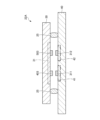
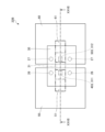
- Fig. 22 is a plan view showing the first example of the configuration of the quantum device 22.
- Fig. 23 is a cross-sectional view showing the first example of the configuration of the quantum device 22.
- Fig. 23 corresponds to a cross-sectional view taken along line XXIII-XXIII in Fig. 22.
- the quantum device 22A of the first example has a quantum bit substrate 30 and a quantum bit substrate 40.
- the quantum bit substrate 30 and the quantum bit substrate 40 are joined to each other via bumps 25.
- the quantum bit substrate 30 is flip-chip bonded to the quantum bit substrate 40.
- the bumps 25 are connected to a ground layer provided on the quantum bit substrate 30 and a ground layer provided on the quantum bit substrate 40.
- the quantum bit substrate 30 includes a coupling flux quantum bit 300, a magnetic flux application unit 330, and a magnetic flux application unit 340.
- the quantum bit substrate 30 has a quantum bit region 31 in which the coupling flux quantum bit 300 is arranged.
- the quantum bit substrate 40 may have wiring or electrodes connected to the flux qubits 100 and 200.
- the quantum bit is not limited to a flux qubit, and may be another quantum bit.
- the quantum bit substrate 40 may have a resonator for observing the state of the quantum bit and an electrode for manipulating the state of the quantum bit.
- a path for introducing a signal for manipulating the state of the quantum bit may be formed by wire bonding from the end of the quantum bit substrate 40, or a through hole may be provided in the quantum bit substrate 40 and a signal may be supplied from the back surface of the quantum bit substrate 40.
- the quantum bit substrate 30 may have a path for supplying a signal at the end or back surface of the quantum bit substrate 30.
- a signal may be supplied from the back surface through the end or through hole of the quantum bit substrate 40 by connecting to a pattern provided on the quantum bit substrate 40 side via a bump.
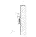
- the quantum bit substrate 30 has, for example, a substrate 80, wiring layers 81, 82, 83, and 84, insulating layers 85, 86, and 87, and a Josephson junction element 88.
- the wiring layer 81 is provided on the substrate 80, and the Josephson junction element 88 is provided on the wiring layer 81.
- the insulating layer 85 is provided on the substrate 80 so as to cover the Josephson junction element 88 and the wiring layer 81.
- the wiring layer 82 is provided on the insulating layer 85 so as to contact the Josephson junction element 88 through an opening formed in the insulating layer 85.
- the insulating layer 86 is provided on the insulating layer 85 so as to cover the wiring layer 82.
- the wiring layer 83 is provided on the insulating layer 86.
- the insulating layer 87 is provided on the insulating layer 86 so as to cover the wiring layer 83.
- the wiring layer 84 is provided on the insulating layer 87 so as to contact the wiring layer 83 through an opening formed in the insulating layer 87.
- the material of the wiring layers 81, 82, 83, and 84 is a material that can become a superconductor, such as niobium or niobium nitride.
- the material of the insulating layers 85, 86, and 87 is, for example, silicon oxide.
- the Josephson junction element 88 has, for example, an aluminum film 88A, an aluminum oxide film 88B, and an aluminum film 88C.
- the aluminum film 88A is connected to the wiring layer 81.
- the aluminum oxide film 88B is provided on the aluminum film 88A.
- the aluminum film 88C is provided on the aluminum oxide film 88B, and the wiring layer 82 is in contact with the aluminum film 88C.
- the Josephson junction element 88 corresponds to the Josephson junction elements 321 and 322.
- the quantum bit substrate 40 includes a charge quantum bit 400, a charge supply unit 430, a charge quantum bit 500, and a charge supply unit 530.
- the quantum bit substrate 40 has a quantum bit region 41 in which the charge quantum bit 400 is arranged, and a quantum bit region 42 in which the charge quantum bit 500 is arranged.
- Figure 25 is a cross-sectional view showing a portion of quantum bit substrate 40.
- Quantum bit substrate 40 has, for example, substrate 90, wiring layers 91 and 92, and insulating layer 93.
- Wiring layer 91 is provided on substrate 90, and insulating layer 93 covers the surface of wiring layer 91.
- Wiring layer 92 is provided on insulating layer 93.
- Wiring layers 91 and 92 and insulating layer 93 form Josephson junction elements corresponding to Josephson junction elements 401, 501.
- Inductor 311 of coupling flux qubit 300 and inductor 403 of charge qubit 400 face each other and are inductively coupled to each other.
- Inductor 312 of coupling flux qubit 300 and inductor 503 of charge qubit 500 face each other and are inductively coupled to each other.
- inductors 311 and 312 of coupling flux quantum bit 300 are connected to wiring layer 84, a part of wiring layer 84 and inductor 403 are inductively coupled to each other, and another part of wiring layer 84 and inductor 503 are inductively coupled to each other.
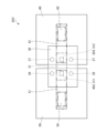
- Fig. 26 is a plan view showing the second example of the configuration of the quantum device 22.
- Fig. 27 is a cross-sectional view showing the second example of the configuration of the quantum device 22.
- Fig. 27 corresponds to a cross-sectional view taken along line XXVII-XXVII in Fig. 26.
- the quantum device 22B of the second example has a quantum bit substrate 30, a quantum bit substrate 50, and a quantum bit substrate 60.
- the quantum bit substrate 30 and the quantum bit substrate 50 are joined to each other via bumps 26, and the quantum bit substrate 30 and the quantum bit substrate 60 are joined to each other via bumps 27.
- the quantum bit substrate 30 is flip-chip bonded to the quantum bit substrates 50 and 60.
- the bumps 26 are connected to a ground layer provided on the quantum bit substrate 30 and a ground layer provided on the quantum bit substrate 50
- the bumps 27 are connected to a ground layer provided on the quantum bit substrate 30 and a ground layer provided on the quantum bit substrate 60.
- the quantum bit substrate 50 includes a charge quantum bit 400 and a charge supply unit 430.
- the quantum bit substrate 50 has a quantum bit region 51 in which the charge quantum bit 400 is arranged.
- the quantum bit substrate 60 includes a charge quantum bit 500 and a charge supply unit 530.
- the quantum bit substrate 60 has a quantum bit region 61 in which the charge quantum bit 500 is arranged.
- Inductor 311 of coupling flux qubit 300 and inductor 403 of charge qubit 400 face each other and are inductively coupled to each other.
- Inductor 312 of coupling flux qubit 300 and inductor 503 of charge qubit 500 face each other and are inductively coupled to each other.
- inductors 311 and 312 of coupling flux quantum bit 300 are connected to wiring layer 84, a portion of wiring layer 83 or 84 is inductively coupled to inductor 403, and another portion of wiring layer 83 or 84 is inductively coupled to inductor 503.
- the quantum bit substrate 50 and the quantum bit substrate 60 may have wiring or electrodes directly or indirectly connected to the quantum bit or the quantum bit.
- the quantum bit substrate 50 and the quantum bit substrate 60 may also have a resonator for observing the state of the quantum bit and an electrode for manipulating the state of the quantum bit.
- a path for introducing a signal for manipulating the state of the quantum bit may be formed by wire bonding from the end of the quantum bit substrate 50 and the quantum bit substrate 60, or a through hole may be provided in the quantum bit substrate 40 and the quantum bit substrate 60 to supply a signal from the back surface of the quantum bit substrate 50 and the quantum bit substrate 60.
- the quantum bit substrate 30 may have a path for supplying a signal at the end or back surface of the quantum bit substrate 30. Also, the signal may be connected to a pattern provided on the quantum bit substrate 50 and the quantum bit substrate 60 side via a bump and supplied from the back surface through the end or through hole of the quantum bit substrate 50 and the quantum bit substrate 60.
- FIG. 28 is a plan view showing the third example of the configuration of the quantum device 22.
- the region 52 of the quantum bit region 51 in which the Josephson junction element 401 and the capacitor 402 are provided is spaced apart from the quantum bit substrate 30 in a planar view. Also, the region 62 of the quantum bit region 61 in which the Josephson junction element 501 and the capacitor 502 are provided is spaced apart from the quantum bit substrate 30 in a planar view.
- the insulating layers 85, 86, and 87 included in the quantum bit substrate 30 can be a source of dielectric loss for the Josephson junction element 401 and the capacitor 402, and for the Josephson junction element 501 and the capacitor 502. In the third example, such dielectric loss can be reduced.
- a ground layer may be provided in the portion of the quantum bit substrate 30 corresponding to the Josephson junction element 401 and the capacitor 402, and the Josephson junction element 501 and the capacitor 502.
- the material of bumps 25, 26, and 27 is preferably a material capable of low-temperature bonding, such as indium or an indium alloy.
- the material of bumps 25, 26, and 27 is preferably a material capable of bonding at 200°C or less, and more preferably a material capable of bonding at 180°C or less.
- the material of bumps 25, 26, and 27 may be a material capable of improving adhesion, such as gold.
- An alloy of indium and gold may also be used. In this case, depending on the composition, it may be capable of bonding at a temperature of 180°C or less and may be a superconducting material.
- the quantum bit substrate 30 and one of the quantum bit substrates 50 and 60 may be connected by a coaxial cable containing a superconducting material (hereinafter, a coaxial cable containing a superconducting material may be referred to as a superconducting cable).
- the superconducting material used in the superconductor cable is, for example, an alloy of niobium and titanium.
- the quantum bit substrate 30 and the quantum bit substrate 50 are joined using bumps 26 as in the second example, and the quantum bit substrate 30 and the quantum bit substrate 60 are coupled by a superconducting cable.
- the inductor 312 of the coupling flux qubit 300 and the superconducting cable are inductively coupled to each other, and the superconducting cable and the inductor 503 of the charge qubit 500 are inductively coupled to each other.
- the quantum bit substrate 30 may be flip-chip bonded to the quantum bit substrate 50.
- the length of the superconducting cable may be several centimeters to several meters, and is typically 1 m to 10 m.
- the coupling state between the charge qubit 400 and the charge qubit 500 can be adjusted by controlling the energy potential of the coupling flux qubit 300.
- the coupling between the superconducting cable and charge qubit 400 or 500 may be capacitive, and the coupling between the superconducting cable and coupling flux qubit 300 may be capacitive.
- a superconducting circuit including a Josephson junction element may also be included in the coupling section, providing direct, inductive, or capacitive coupling.
- the quantum bit substrate 30 and the quantum bit substrate 60 may be joined using bumps 27 as in the second example, and the quantum bit substrate 30 and the quantum bit substrate 50 may be connected by a superconducting cable. Also, the quantum bit substrate 30 and the quantum bit substrates 50 and 60 may be connected by a superconducting cable.
- quantum bit substrates By connecting quantum bit substrates using superconducting cables, it is possible to increase the freedom of arrangement of quantum bit substrates on stages inside the same dilution refrigerator. For example, when placing quantum bit substrates on the lowest temperature stage of a dilution refrigerator, quantum bit substrates can be placed at distant locations and protected by different magnetic shields. In addition, by using long superconducting cables of 5 to 10 meters, quantum bits on quantum bit substrates installed in different dilution refrigerators can be connected to each other.
- the magnetic flux application unit 330 applies a magnetic flux of ⁇ 0 to the coupling flux qubit 300
- an unstable state does not clearly appear in the shape of the energy potential of the coupling flux qubit 300 (see FIG. 6 ).
- the value of the variable ⁇ L expressed by 2 ⁇ LI C / ⁇ 0 is 1.2 to 8.0.
- L is the total inductance of the coupling flux qubit 300
- I C is the sum of the critical current values of the Josephson junction elements 321 and 322. It is more preferable that the value of the variable ⁇ L is 1.2 to 6.0, since an inflection point that is a sign of an unstable state appearing in the energy potential does not clearly appear.
- the critical current value I C of Josephson junction elements 321 and 322 may be 1.0 ⁇ A to 4.0 ⁇ A.
- the smaller the critical current value I C the easier it is to widen the range of selection for the overall inductance L of coupling flux qubit 300.
- the larger the critical current value I C the narrower the range of selection for inductance L, but the easier it is to stably form Josephson junction elements 321 and 322.
- the applied flux is 0.5 ⁇ 0 , but it does not have to be 0.5 ⁇ 0 strictly, and may be 0.4 ⁇ 0 to 0.6 ⁇ 0 .
- the coupling flux quantum bit 300 may have multiple SQUIDs 320 connected in parallel to each other. In this case, the variation in characteristics can be reduced.
- the coupling flux qubit 300 does not have to include the flux application section 340.
- quantum computing system and quantum device disclosed herein can be used, for example, in quantum computing.
- quantum computing system 10 control units 21, 22, 22A, 22B, 22C: quantum devices 30, 40, 50, 60: quantum bit substrates 31, 41, 42, 51, 61: quantum bit regions 100
- 200 flux qubits 110, 210, 310: main loop 120, 220, 320: SQUID 130, 140, 230, 240, 330, 340: magnetic flux application unit 300: coupling flux quantum bit 400, 500: charge quantum bit 430, 530: charge supply unit
Landscapes
- Engineering & Computer Science (AREA)
- General Physics & Mathematics (AREA)
- Theoretical Computer Science (AREA)
- Physics & Mathematics (AREA)
- Mathematical Analysis (AREA)
- Data Mining & Analysis (AREA)
- Evolutionary Computation (AREA)
- Condensed Matter Physics & Semiconductors (AREA)
- Computational Mathematics (AREA)
- Mathematical Optimization (AREA)
- Pure & Applied Mathematics (AREA)
- Computing Systems (AREA)
- General Engineering & Computer Science (AREA)
- Mathematical Physics (AREA)
- Software Systems (AREA)
- Artificial Intelligence (AREA)
- Superconductor Devices And Manufacturing Methods Thereof (AREA)
Abstract
Description
本開示は、量子演算システム及び量子デバイスの制御方法に関する。 This disclosure relates to a quantum computing system and a method for controlling a quantum device.
従来、磁束量子ビットを用いて二つの磁束量子ビットを結合することが可能な量子演算システムが提案されている。 Conventionally, quantum computing systems have been proposed that can couple two flux qubits using flux qubits.
従来の量子演算システムでは、量子ビットの間の結合を切ることができず、不必要な結合により相互作用が生じるおそれがある。 In conventional quantum computing systems, it is not possible to break the bonds between quantum bits, and there is a risk that unnecessary bonds could cause interactions.
本開示の目的は、二つの量子ビットの結合をオフすることができる量子演算システム及び量子デバイスの制御方法を提供することにある。 The objective of this disclosure is to provide a quantum computing system and a method for controlling a quantum device that can turn off the coupling between two quantum bits.
本開示の一形態によれば、量子デバイスと、前記量子デバイスを制御する制御部と、を有し、前記量子デバイスは、第1量子ビットと、第2量子ビットと、前記第1量子ビット及び前記第2量子ビットと結合可能な結合用磁束量子ビットと、前記結合用磁束量子ビットに磁束を印加する第1磁束印加部と、を有し、前記制御部は、前記第1磁束印加部に、第1期間において、第1時間変調を備えた第1磁束を印加させ、前記第1期間とは異なる第2期間において、前記第1時間変調とは異なる第2時間変調を備えた第2磁束を印加させる、量子演算システムが提供される。 According to one embodiment of the present disclosure, there is provided a quantum computing system comprising a quantum device and a control unit that controls the quantum device, the quantum device comprising a first quantum bit, a second quantum bit, a coupling flux qubit that can be coupled to the first quantum bit and the second quantum bit, and a first flux application unit that applies a magnetic flux to the coupling flux qubit, and the control unit causes the first flux application unit to apply a first magnetic flux having a first time modulation in a first period, and to apply a second magnetic flux having a second time modulation different from the first time modulation in a second period different from the first period.
本開示によれば、二つの量子ビットの結合をオフすることができる。 According to this disclosure, it is possible to turn off the coupling between two quantum bits.
以下、本開示の実施形態について添付の図面を参照しながら具体的に説明する。なお、本明細書及び図面において、実質的に同一の機能構成を有する構成要素については、同一の符号を付することにより重複した説明を省くことがある。 Below, an embodiment of the present disclosure will be specifically described with reference to the attached drawings. Note that in this specification and drawings, components having substantially the same functional configurations may be given the same reference numerals to avoid redundant description.
(第1実施形態)
まず、第1実施形態について説明する。第1実施形態は量子演算システムに関する。図1は、第1実施形態に係る量子演算システムを示すブロック図である。
First Embodiment
First, a first embodiment will be described. The first embodiment relates to a quantum computing system. Fig. 1 is a block diagram showing a quantum computing system according to the first embodiment.
第1実施形態に係る量子演算システム1は、制御部10と、量子デバイス21とを有する。制御部10は、量子デバイス21を制御する。
The
制御部10はコンピュータであり、バス11と、入力装置12と、出力装置13と、記憶装置14と、メモリ装置15と、演算処理装置16と、インタフェース装置17とを含む。入力装置12、出力装置13、記憶装置14、メモリ装置15、演算処理装置16及びインタフェース装置17がバス11に接続されている。入力装置12、出力装置13、記憶装置14、メモリ装置15、演算処理装置16及びインタフェース装置17はバス11を介して相互に接続されている。
The
入力装置12は、各種の情報の入力を行うための装置であり、例えばキーボードやポインティングデバイス等により実現される。出力装置13は、各種の情報の出力を行うためものであり、例えばディスプレイ等により実現される。インタフェース装置17は、LANカード等を含み、ネットワークに接続するために用いられる。
The
記憶装置14に、量子デバイス21を制御するための制御プログラムが格納されている。メモリ装置15は、量子演算システム1の起動時に記憶装置14から制御プログラムを読み出して格納する。そして、演算処理装置16はメモリ装置15に格納された制御プログラムに従って、後述するような各種処理を実現する。
The
図2は、量子デバイス21を示す回路図である。量子デバイス21は、磁束量子ビット100と、磁束量子ビット200と、結合用磁束量子ビット300とを有する。結合用磁束量子ビット300は、磁束量子ビット100及び200と誘導結合可能である。ここでは磁束量子ビット100と磁束量子ビット200とを誘導結合する例を開示するが、結合の形態としては容量結合でもよく、誘導結合と容量結合を含むものであってもよい。量子デバイス21は、更に、磁束印加部130、140、230、240、330及び340を有する。
FIG. 2 is a circuit diagram showing
磁束量子ビット100は、メインループ110と、超伝導量子干渉磁束計(superconducting quantum interference device:SQUID)120とを有する。SQUID120は、この順で環状かつ直列に接続されたジョセフソン接合素子121と、ジョセフソン接合素子122と、インダクタ123と、インダクタ124とを有する。メインループ110は、互いに直列に接続されたインダクタ112及び113を有する。インダクタ112のインダクタ113とは反対側の端部がジョセフソン接合素子121とジョセフソン接合素子122との間に接続されている。インダクタ113のインダクタ112とは反対側の端部がインダクタ123とインダクタ124との間に接続されている。例えば、磁束量子ビット100は超伝導材料としてニオブを含む。磁束量子ビット100は第1量子ビット及び第1磁束量子ビットの一例である。
The
磁束量子ビット200は、メインループ210と、SQUID220とを有する。SQUID220は、この順で環状かつ直列に接続されたジョセフソン接合素子221と、ジョセフソン接合素子222と、インダクタ223と、インダクタ224とを有する。メインループ210は、互いに直列に接続されたインダクタ212及び213を有する。インダクタ213のインダクタ212とは反対側の端部がジョセフソン接合素子221とジョセフソン接合素子222との間に接続されている。インダクタ212のインダクタ213とは反対側の端部がインダクタ223とインダクタ224との間に接続されている。例えば、磁束量子ビット200は超伝導材料としてニオブを含む。磁束量子ビット200は第2量子ビット及び第2磁束量子ビットの一例である。
結合用磁束量子ビット300は、メインループ310と、SQUID320とを有する。SQUID320は、この順で環状かつ直列に接続されたジョセフソン接合素子321と、ジョセフソン接合素子322と、インダクタ323と、インダクタ324とを有する。メインループ310は、この順で直列に接続されたインダクタ311、313及び312を有する。インダクタ312のインダクタ313とは反対側の端部がジョセフソン接合素子321とジョセフソン接合素子322との間に接続されている。インダクタ311のインダクタ313とは反対側の端部がインダクタ323とインダクタ324との間に接続されている。インダクタ311とインダクタ112とが互いに誘導結合され、インダクタ312とインダクタ212とが互いに誘導結合されている。
The
磁束印加部130は、インダクタ131及び132と、パルス信号発生器133とを有する。インダクタ131及び132は互いに直列に接続されている。インダクタ132のインダクタ131とは反対側の端部は接地されている。インダクタ131のインダクタ132とは反対側の端部と接地との間にパルス信号発生器133が接続されている。インダクタ131とインダクタ123とが互いに誘導結合されている。インダクタ132とインダクタ124とが互いに誘導結合されている。磁束印加部130は第2磁束印加部の一例である。
The magnetic
磁束印加部230は、インダクタ231及び232と、パルス信号発生器233とを有する。インダクタ231及び232は互いに直列に接続されている。インダクタ231のインダクタ232とは反対側の端部は接地されている。インダクタ232のインダクタ231とは反対側の端部と接地との間にパルス信号発生器233が接続されている。インダクタ231とインダクタ223とが互いに誘導結合されている。インダクタ232とインダクタ224とが互いに誘導結合されている。磁束印加部230は第3磁束印加部の一例である。
The magnetic
磁束印加部330は、インダクタ331及び332と、パルス信号発生器333とを有する。インダクタ331及び332は互いに直列に接続されている。インダクタ332のインダクタ331とは反対側の端部は接地されている。インダクタ331のインダクタ332とは反対側の端部と接地との間にパルス信号発生器333が接続されている。インダクタ331とインダクタ323とが互いに誘導結合されている。インダクタ332とインダクタ324とが互いに誘導結合されている。磁束印加部330は第1磁束印加部の一例である。
The magnetic
磁束印加部140は、インダクタ141と、直流電源142とを有する。インダクタ141と直流電源142の正極とが互いに接続されている。インダクタ141の直流電源142とは反対側の端部は接地されている。直流電源142の負極は接地されている。インダクタ141とインダクタ113とが互いに誘導結合されている。メインループ310は環状配線の一例である。
The magnetic
磁束印加部240は、インダクタ241と、直流電源242とを有する。インダクタ241と直流電源242の正極とが互いに接続されている。インダクタ241の直流電源242とは反対側の端部は接地されている。直流電源242の負極は接地されている。インダクタ241とインダクタ213とが互いに誘導結合されている。
The magnetic
磁束印加部340は、インダクタ341と、直流電源342とを有する。インダクタ341と直流電源342の正極とが互いに接続されている。インダクタ341の直流電源342とは反対側の端部は接地されている。直流電源342の負極は接地されている。インダクタ341とインダクタ313とが互いに誘導結合されている。
The magnetic
制御部10は、第1期間において磁束量子ビット100と磁束量子ビット200との結合をオン状態とし、第2期間において磁束量子ビット100と磁束量子ビット200との結合をオフ状態とする。図3は、第1期間においてSQUID120、220及び320に印加される磁束の時間変化を示すタイミングチャートである。図4は、第2期間においてSQUID120、220及び320に印加される磁束の時間変化を示すタイミングチャートである。図5及び図6は、磁束量子ビットのエネルギー状態を示す図である。図3及び図4中において、Φ120はSQUID120に印加される磁束を示し、Φ220はSQUID220に印加される磁束を示し、Φ320はSQUID320に印加される磁束を示す。Φ0は磁束量子である。図5及び図6における横軸は、メインループに印加される磁束を示す。
The
なお、図2では、いくつかのインダクタ、例えばインダクタ123及び124を個別のインダクタとして開示しているが、これらを一体的に形成したインダクタを用いてもよい。また、いくつかの直流電源、例えば直流電源142は電源の一例であり、他の形態の電源、例えば任意波形源であってもよい。また、磁束量子ビット200と結合用磁束量子ビット300との間の結合は間接的な結合であり、誘導的な結合、容量的な結合、その他の結合であってもよい。
Note that although FIG. 2 shows some inductors, such as
図3に示すように、第1期間では、制御部10の制御により、磁束Φ120、Φ220及びΦ320のいずれもが、時刻t12までは0(Wb)で、時刻t12から時刻t13までΦ0まで上昇し、時刻t13からはΦ0となる。磁束Φ320の上昇は、時間に対して直線的でなくてもよい。なお、結合用磁束量子ビット300のエネルギーポテンシャルはΦ=0(Wb)の場合とΦ=Φ0の場合において互いに等価である。そのため、磁束Φ320を時刻t12までΦ0に維持し、時刻t12から時刻t13までの間に0(Wb)まで下降させ、時刻t13以降を0(Wb)に制御してもよい。
As shown in Fig. 3, in the first period, under the control of the
図4に示すように、第2期間では、制御部10の制御により、磁束Φ120及びΦ220のいずれもが、時刻t22までは0(Wb)で、時刻t22から時刻t23までΦ0まで上昇し、時刻t23からはΦ0となる。一方、制御部10の制御により、磁束Φ320は、時刻t22よりも前の時刻t21までは0(Wb)で、時刻t21から時刻t22まで0.5Φ0まで上昇し、時刻t22からは0.5Φ0となる。なお、磁束Φ320を時刻t22より以前に0.5Φ0になるように制御してもよい。
4, in the second period, under the control of the
磁束量子ビット100、磁束量子ビット200及び結合用磁束量子ビット300のいずれの磁束量子ビットにおいても、印加される磁束がΦ0となると、図6に示すように、基底状態が二つとなる。また、磁束量子ビット100、磁束量子ビット200及び結合用磁束量子ビット300のいずれの磁束量子ビットにおいても、印加される磁束が0.5Φ0となると、図5に示すように、基底状態が一つとなる。ここで、図5に示されるようにエネルギーの基底状態が一つとなる場合の基底状態のエネルギー値は低くなる。一方、図6に示されるように、エネルギーの基底状態が二つとなる場合の基底状態のエネルギー値は図5の状態よりも高い。時刻t22と時刻t23の間の期間において、結合用磁束量子ビット300が図5の状態となると、磁束量子ビット100及び磁束量子ビット200との間にエネルギーポテンシャルの違いがあると、磁束量子ビット100と磁束量子ビット200との間に量子トンネル現象が起きにくくなる。そのため、磁束量子ビット100と磁束量子ビット200との間の結合をオフに制御しやすくなる。
In any of the flux qubits,
従って、第1期間では、磁束Φ120、Φ220及びΦ320が同時に0.5Φ0となり、磁束Φ120、Φ220及びΦ320が0.5Φ0の時に磁束量子ビット100と磁束量子ビット200とが重ね合わせの状態となる。その後、磁束Φ120、Φ220及びΦ320がΦ0まで上昇すると、磁束量子ビット100及び200が古典的な状態になり、解が収束する。このため、第1期間では、磁束量子ビット100と磁束量子ビット200との結合がオン状態となる。
Therefore, in the first period, the magnetic fluxes Φ120, Φ220, and Φ320 are simultaneously 0.5Φ0 , and when the magnetic fluxes Φ120, Φ220, and Φ320 are 0.5Φ0 , the
一方、第2期間では、磁束Φ120及びΦ220が0.5Φ0となる前に、磁束Φ320が0.5Φ0となり、磁束量子ビット100と磁束量子ビット200とが重ね合わせの状態となる期間がない。このため、第2期間では、磁束量子ビット100と磁束量子ビット200との結合がオフ状態となる。
On the other hand, in the second period, before the magnetic fluxes Φ120 and Φ220 become 0.5Φ 0 , there is no period during which the magnetic flux Φ320 becomes 0.5Φ 0 and the
(第1シミュレーション)
次に、本願発明者が行った第1実施形態に関する第1シミュレーションについて説明する。第1シミュレーションでは、磁束印加部140の制御により磁束量子ビット100を「1」状態をとりやすい状態とし、磁束印加部240の制御により磁束量子ビット200に2種類のバイアスを付与した。一方のバイアスでは、磁束量子ビット200の「1」状態の確率が50%となるようにし、他方のバイアスでは、磁束量子ビット200が「0」状態となりやすいようにした。そして、上記の第1期間、第2期間の制御を行った。また、参考のために、結合用磁束量子ビット300がないこととして、磁束Φ120及びΦ220を第1期間と同様に変化させた。
(First Simulation)
Next, a first simulation of the first embodiment performed by the present inventor will be described. In the first simulation,
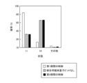
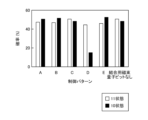
第1シミュレーションでは試行回数を1000回とした。第1シミュレーションの結果を図7及び図8に示す。図7は、磁束量子ビット200の「1」状態の確率が50%となるようにした場合の結果を示し、図8は、磁束量子ビット200が「0」状態となりやすいようにした場合の結果を示す。図7及び図8中の「11」は磁束量子ビット100及び磁束量子ビット200の両方が「1」状態であることを示し、「10」は磁束量子ビット100が「1」状態、磁束量子ビット200が「0」状態であることを示す。
In the first simulation, the number of trials was 1000. The results of the first simulation are shown in Figures 7 and 8. Figure 7 shows the results when the probability of
図7に示すように、磁束量子ビット200の「1」状態の確率が50%となるようにした場合でも、第1期間の制御が行われると、高確率で磁束量子ビット200も「1」状態となった。また、第2期間の制御が行われると、結合用磁束量子ビット300を動作させないときと同様の結果が得られた。
As shown in FIG. 7, even when the probability of the
図8に示すように、磁束量子ビット200が「0」状態となりやすいようにした場合でも、第1期間の制御が行われると、高確率で磁束量子ビット200も「1」状態となった。また、第2期間の制御が行われると、結合用磁束量子ビット300を動作させないときと同様の結果が得られた。
As shown in FIG. 8, even when the
以上のことから、第1期間では、磁束量子ビット100と磁束量子ビット200との結合がオン状態となり、第2期間では、磁束量子ビット100と磁束量子ビット200との結合がオフ状態となるといえる。
From the above, it can be said that in the first period, the coupling between
(第2シミュレーション)
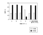
次に、本願発明者が行った第1実施形態に関する第2シミュレーションについて説明する。第2シミュレーションでは、第2期間の制御として種々の制御を行った。また、第2シミュレーションでも、第1シミュレーションと同様に、磁束印加部140の制御により磁束量子ビット100を「1」状態をとりやすい状態とし、磁束印加部240の制御により磁束量子ビット200に2種類のバイアスを付与した。一方のバイアスでは、磁束量子ビット200の「1」状態の確率が50%となるようにし、他方のバイアスでは、磁束量子ビット200の「0」状態の確率が70%となるようにした。図9~図12は、第2シミュレーションでの、第2期間においてSQUID120、220及び320に印加される磁束の時間変化を示すタイミングチャートである。図9~図12に示す制御パターンにおいて、SQUID120及び220に印加される磁束の時間変化は、図4に示す制御パターンCと同一である。
(Second Simulation)
Next, a second simulation of the first embodiment performed by the inventors of the present application will be described. In the second simulation, various controls were performed as the control of the second period. In the second simulation, similar to the first simulation, the
図9に示す制御パターンAでは、磁束Φ320を常時0(Wb)とした。 In control pattern A shown in Figure 9, the magnetic flux Φ320 is always set to 0 (Wb).
図10に示す制御パターンBでは、磁束Φ320を時刻t22までは0(Wb)で、時刻t22から時刻t23まで0.5Φ0まで上昇させ、時刻t23からは0.5Φ0とした。 In the control pattern B shown in FIG. 10, the magnetic flux Φ320 is 0 (Wb) until time t22, increased to 0.5Φ0 from time t22 to time t23, and set to 0.5Φ0 from time t23.
先に示した図4に示す制御パターンCでは、磁束Φ320を時刻t21までは0(Wb)で、時刻t21から時刻t22まで0.5Φ0まで上昇させ、時刻t22からは0.5Φ0とした。 In the control pattern C shown in FIG. 4 previously described, the magnetic flux Φ320 is 0 (Wb) until time t21, increased to 0.5Φ0 from time t21 to time t22, and set to 0.5Φ0 from time t22.
図11に示す制御パターンDでは、磁束Φ320を時刻t22まではΦ0で、時刻t22から時刻t23まで0.5Φ0まで下降させ、時刻t23からは0.5Φ0とした。 In the control pattern D shown in FIG. 11, the magnetic flux Φ320 is Φ0 until time t22, is decreased to 0.5Φ0 from time t22 to time t23, and is set to 0.5Φ0 from time t23.
図12に示す制御パターンEでは、磁束Φ320を時刻t22まではΦ0で、時刻t22から時刻t23まで0(Wb)まで下降させ、時刻t23からは0(Wb)とした。 In the control pattern E shown in FIG. 12, the magnetic flux Φ320 is Φ0 until time t22, is decreased to 0 (Wb) from time t22 to time t23, and is kept at 0 (Wb) from time t23.
第2シミュレーションでは試行回数を1000回とした。第2シミュレーションの結果を図13及び図14に示す。図13は、磁束量子ビット200の「1」状態の確率が50%となるようにした場合の結果を示し、図14は、磁束量子ビット200の「0」状態の確率が70%となるようにした場合の結果を示す。図13及び図14中の「11」は磁束量子ビット100及び磁束量子ビット200の両方が「1」状態であることを示し、「10」は磁束量子ビット100が「1」状態、磁束量子ビット200が「0」状態であることを示す。
In the second simulation, the number of trials was 1000. The results of the second simulation are shown in Figures 13 and 14. Figure 13 shows the results when the probability of
図13及び図14に示すように、制御パターンB及びCにおいて、結合用磁束量子ビット300がないこととして、磁束Φ120及びΦ220を第1期間と同様に変化させた場合と近い結果が得られた。特に制御パターンCは、結合用磁束量子ビット300がないこととした場合と最も近い結果が得られた。結合用磁束量子ビット300のエネルギーポテンシャルが図5に示されるように基底状態が一つとなるように磁束をバイアスされた状態である制御パターンB及び制御パターンCにおいては、磁束がバイアスされていない状態である制御パターンAよりも、外部からの突発的な磁束変化に対して耐性が強く、安定性に優れている。また、制御パターンB及び制御パターンCでは、時刻t22と時刻t23との間の期間において、磁束量子ビット100及び磁束量子ビット200と、結合用磁束量子ビット300との間にエネルギーポテンシャルの違いがあるため量子トンネル効果が小さくなる。そのため、制御パターンB及び制御パターンCは、制御パターンAの場合よりも磁束量子ビット100と磁束量子ビット200との間の結合をオフに制御しやすくなる。
13 and 14, in control patterns B and C, results similar to those obtained when coupling
(第3シミュレーション)
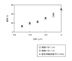
次に、本願発明者が行った第1実施形態に関する第3シミュレーションについて説明する。第3シミュレーションでは、磁束印加部240に流すバイアス電流I240を変化させながら、制御パターンA及びCと、結合用磁束量子ビット300がないこととした場合との間での結果を比較した。第3シミュレーションでは試行回数を1000回とした。第3シミュレーションの結果を図15及び図16に示す。図15の縦軸は、磁束量子ビット100及び磁束量子ビット200の両方が「1」状態である「11」状態となる確率を示す。図16の縦軸は、磁束量子ビット100が「1」状態、磁束量子ビット200が「0」状態である「10」状態となる確率を示す。
(Third Simulation)
Next, a third simulation of the first embodiment performed by the inventors of the present application will be described. In the third simulation, the bias current I240 flowing through the
図15及び図16に示すように、制御パターンCによれば制御パターンAよりも、結合用磁束量子ビット300がないこととした場合に近い結果が得られた。
As shown in Figures 15 and 16, control pattern C produced results closer to those obtained when coupling
以上のシミュレーションの結果から、制御パターンCが特に好ましい。磁束量子ビット100及び磁束量子ビット200のエネルギーポテンシャルの変化を考慮すると、磁束Φ120及びΦ220が0.3Φ0になる前に磁束Φ320が0.4Φ0~0.6Φ0になっていることが好ましい。
From the above simulation results, control pattern C is particularly preferable. Considering the changes in the energy potential of
なお、磁束の変化は、例えば0.1ns~100msの時間で行われてもよく、1μs~1msで行われてもよい。 The change in magnetic flux may occur over a period of, for example, 0.1 ns to 100 ms, or 1 μs to 1 ms.
(第2実施形態)
次に、第2実施形態について説明する。第2実施形態は量子演算システムに関する。図17は、第2実施形態に係る量子演算システムを示すブロック図である。
Second Embodiment
Next, a second embodiment will be described. The second embodiment relates to a quantum processing system. Fig. 17 is a block diagram showing a quantum processing system according to the second embodiment.
第2実施形態に係る量子演算システム2は、制御部10と、量子デバイス21とを有する。制御部10は、量子デバイス21を制御する。制御部10の構成は、制御プログラムの内容を除き第1実施形態と同様である。
The
図18は、量子デバイス22を示す回路図である。量子デバイス22は、電荷量子ビット400と、電荷量子ビット500と、結合用磁束量子ビット300とを有する。結合用磁束量子ビット300は、電荷量子ビット400及び500と誘導結合可能である。量子デバイス22は、更に、電荷供給部430及び530を有する。結合用磁束量子ビット300の構成は第1実施形態と同様である。
FIG. 18 is a circuit diagram showing
電荷量子ビット400は、例えばトランズモン量子ビットであり、互いに環状に接続されたジョセフソン接合素子401と、キャパシタ402とを有する。電荷量子ビット400は、更に、ジョセフソン接合素子401及びキャパシタ402に電気的に並列に接続されたインダクタ403を有する。インダクタ403とインダクタ311とは互いに誘導結合されている。ジョセフソン接合素子401、キャパシタ402及びインダクタ403の一端が接地されている。例えば、電荷量子ビット400は超伝導材料として窒化チタンを含む。電荷量子ビット400は第1量子ビット及び第1電荷量子ビットの一例である。なお、ジョセフソン接合素子401、キャパシタ402及びインダクタ403の一端を接地することは必須ではなく、また、接地する場合も、容量を介して接地面に接続されてもよい。
The
ジョセフソン接合素子401、キャパシタ402及びインダクタ403の他端に電荷供給部430が接続されている。電荷供給部430は、電流源431と、キャパシタ432とを有する。電流源431の一端とジョセフソン接合素子401、キャパシタ402及びインダクタ403と間にキャパシタ432が接続されている。電流源431の他端は接地されている。
The
電荷量子ビット500は、例えばトランズモン量子ビットであり、互いに環状に接続されたジョセフソン接合素子501と、キャパシタ502とを有する。電荷量子ビット500は、更に、ジョセフソン接合素子501及びキャパシタ502に電気的に並列に接続されたインダクタ503を有する。インダクタ503とインダクタ312とは互いに誘導結合されている。ジョセフソン接合素子501、キャパシタ502及びインダクタ503の一端が接地されている。例えば、電荷量子ビット500は超伝導材料として窒化チタンを含む。電荷量子ビット500は第2量子ビット及び第2電荷量子ビットの一例である。
The
ジョセフソン接合素子501、キャパシタ502及びインダクタ503の他端に電荷供給部530が接続されている。電荷供給部530は、電流源531と、キャパシタ532とを有する。電流源531の一端とジョセフソン接合素子501、キャパシタ502及びインダクタ503と間にキャパシタ532が接続されている。電流源531の他端は接地されている。
A
制御部10は、第1期間において電荷量子ビット400と電荷量子ビット500との結合をオン状態とし、第2期間において電荷量子ビット400と電荷量子ビット500との結合をオフ状態とする。図19は、第1期間において電流源431が発生する電流、電流源531が発生する電流及びSQUID320に印加される磁束の時間変化を示すタイミングチャートである。図20は、第2期間において電流源431が発生する電流、電流源531が発生する電流及びSQUID320に印加される磁束の時間変化を示すタイミングチャートである。図19及び図20中において、I431は電流源431が発生する電流を示し、I531は電流源531が発生する電流を示し、Φ320はSQUID320に印加される磁束を示す。
電荷量子ビット400と電荷量子ビット500との結合をオン状態として電荷量子ビット400にゲート操作を行う場合について、図19を用いて説明する。この例では、時刻t31から時刻t32の期間が第1期間に対応する。図19に示すように、第1期間では、制御部10の制御により、時刻t31から時刻t32の時間を含むように、電流源431がゲート操作のための電流を発生する。電流源431が電流を発生している間、電荷量子ビット400のゲート操作が行われる。制御部10の制御により、磁束Φ320は時刻t30から時刻t31の時間に0.5Φ0となる。電流源531が発生する電流は常時0(A)とする。次に、時刻t31と時刻t32の間の期間、磁束Φ320を0(Wb)とする。この期間において電荷量子ビット400と電荷量子ビット500との間の結合はオン状態となる。その後、時刻t32以降、再び磁束Φ320を0.5Φ0とする。時刻t32以降、磁束Φ320を0.5Φ0に戻すことが好ましいが、時刻t32以降も磁束Φ320を0(Wb)に維持してもよい。なお、結合用磁束量子ビット300のエネルギーポテンシャルに関し、Φ=0(Wb)の場合とΦ=Φ0の場合とでは等価であるため、時刻t31と時刻t32の間の期間、磁束Φ320をΦ=Φ0としてもよい。
A case where the coupling between the
次に、電荷量子ビット400と電荷量子ビット500との結合をオフ状態として電荷量子ビット400にゲート操作を行う場合について、図20を用いて説明する。この例では、時刻t31から時刻t32の期間が第2期間に対応する。図20に示すように、制御部10の制御により、時刻t31から時刻t32の期間を含むように、電流源431がゲート操作のための電流を発生する。電流源431が電流を発生している間、電荷量子ビット400のゲート操作が行われる。制御部10の制御により、磁束Φ320は時刻t31から時刻t32までの期間(第2期間)、0.5Φ0となる。電流源531が発生する電流は常時0(A)とする。なお、図20においては、時刻t30から時刻t31までの期間、及び時刻t32以降の期間も磁束Φ320を0.5Φ0となるよう制御する例を示している。
Next, a case where the coupling between the
上記のように、結合用磁束量子ビット300において、印加される磁束が0(Wb)又はΦ0となると、図6に示すように、基底状態が二つとなり、印加される磁束が0.5Φ0となると、図5に示すように、基底状態が一つとなる。ここで、結合用磁束量子ビット300において印加される磁束を0(Wb)又はΦ0とすると結合をオン状態に制御でき、印加される磁束を0.5Φ0とすると結合をオフ状態に制御することができることについて説明する。
As described above, in
図21は、結合用磁束量子ビット300の磁束と、結合される電荷量子ビット400の内部電流との関係を示す図である。図21は、電荷量子ビット400及び電荷量子ビット500の共鳴周波数を8.1GHzとしてシミュレーションを行って得られた結果を示す。電荷量子ビット500に対して信号源としての電流源531から8.1GHzの励起信号を印加した際に、電荷量子ビット400の内部状態を計算し、内部電流Ipを観測した。その際、結合用磁束量子ビット300に印加する信号(パルス信号発生器333の出力信号)の強度を変調した。
Figure 21 shows the relationship between the magnetic flux of
図21の縦軸には、信号の大きさが0の時の内部電流Ipを基準として、信号強度(パルス信号発生器333によって印加される磁束)に応じた内部電流Ipを規格化した値が示されている。磁束を0(Wb)とした時に、電荷量子ビット400と電荷量子ビット500との間の結合がオン状態である一方で、磁束を0.5Φ0とした時に、結合がオフ状態となっていることが分かる。
21 shows a normalized value of the internal current Ip according to the signal strength (magnetic flux applied by the pulse signal generator 333) with reference to the internal current Ip when the signal magnitude is 0. It can be seen that when the magnetic flux is 0 (Wb), the coupling between the
電荷量子ビット400及び電荷量子ビット500に代えてXmonを用いた場合においても、共鳴周波数は異なるが、図21と同じ傾向となることがシミュレーションで確認された。
Even when Xmon is used instead of charge
Xmonは、単層配線で構成された磁束量子ビットであり、例えば、超伝導材料としてニオブ、窒化チタン又は窒化ニオブを含む。また、結合用磁束量子ビット300と電荷量子ビット400及び500との結合が容量結合であってもよい。
Xmon is a flux qubit made of a single-layer wiring, and contains, for example, niobium, titanium nitride, or niobium nitride as a superconducting material. In addition, the coupling between the
(量子デバイス22の構成の第1例)
次に、量子デバイス22の構成の第1例について説明する。図22は、量子デバイス22の構成の第1例を示す平面図である。図23は、量子デバイス22の構成の第1例を示す断面図である。図23は、図22中のXXIII-XXIII線に沿った断面図に相当する。
(First Example of the Configuration of the Quantum Device 22)
Next, a first example of the configuration of the
図22及び図23に示すように、第1例の量子デバイス22Aは、量子ビット基板30と、量子ビット基板40とを有する。量子ビット基板30と量子ビット基板40とが、バンプ25を介して互いに接合されている。例えば、量子ビット基板30が量子ビット基板40にフリップチップボンディングされている。例えば、バンプ25は量子ビット基板30に設けられた接地層と、量子ビット基板40に設けられた接地層とに接続されている。
As shown in Figures 22 and 23, the
量子ビット基板30は、結合用磁束量子ビット300と、磁束印加部330と、磁束印加部340とを含む。量子ビット基板30は、結合用磁束量子ビット300が配置された量子ビット領域31を有する。
The
なお、図23に図示されていないが、量子ビット基板40は磁束量子ビット100、200に接続される配線や電極を有していてもよい。量子ビットは、磁束量子ビットに限られず、他の量子ビットでもよい。また、量子ビット基板40は、量子ビットの状態を観測するための共振器や、量子ビットの状態を操作するための電極を有していてもよい。更に、量子ビットの状態を操作する信号を導入する経路を量子ビット基板40の端部からワイヤボンディングで形成してもよく、量子ビット基板40に貫通孔を設けて量子ビット基板40の裏面から信号を供給してもよい。量子ビット基板30は信号を供給する経路を量子ビット基板30の端部や裏面に有していてもよい。また、バンプを介して量子ビット基板40側に設けたパターンと接続し、量子ビット基板40の端部や貫通孔を介して裏面から供給してもよい。
23, the
図24は、量子ビット基板30の一部を示す断面図である。量子ビット基板30は、例えば、基板80と、配線層81、82、83及び84と、絶縁層85、86及び87と、ジョセフソン接合素子88とを有する。配線層81は基板80の上に設けられ、ジョセフソン接合素子88は配線層81の上に設けられている。絶縁層85はジョセフソン接合素子88及び配線層81を覆うようにして基板80の上に設けられている。配線層82は、絶縁層85に形成された開口部を通じてジョセフソン接合素子88に接するようにして絶縁層85の上に設けられている。絶縁層86は配線層82を覆うようにして絶縁層85の上に設けられている。配線層83は絶縁層86の上に設けられている。絶縁層87は配線層83を覆うようにして絶縁層86の上に設けられている。配線層84は、絶縁層87に形成された開口部を通じて配線層83に接するようにして絶縁層87の上に設けられている。配線層81、82、83及び84の材料は、例えばニオブ又は窒化ニオブ等の超伝導体となり得る材料である。絶縁層85、86及び87の材料は、例えば酸化シリコンである。
24 is a cross-sectional view showing a part of the
ジョセフソン接合素子88は、例えば、アルミニウム膜88Aと、酸化アルミニウム膜88Bと、アルミニウム膜88Cとを有する。アルミニウム膜88Aは配線層81に接続されている。酸化アルミニウム膜88Bはアルミニウム膜88Aの上に設けられている。アルミニウム膜88Cは酸化アルミニウム膜88Bの上に設けられており、アルミニウム膜88Cに配線層82が接している。ジョセフソン接合素子88は、ジョセフソン接合素子321、322に相当する。
The
量子ビット基板40は、電荷量子ビット400と、電荷供給部430と、電荷量子ビット500と、電荷供給部530とを含む。量子ビット基板40は、電荷量子ビット400が配置された量子ビット領域41と、電荷量子ビット500が配置された量子ビット領域42とを有する。
The
図25は、量子ビット基板40の一部を示す断面図である。量子ビット基板40は、例えば、基板90と、配線層91及び92と、絶縁層93とを有する。配線層91は基板90の上に設けられ、絶縁層93は配線層91の表面を覆う。配線層92は絶縁層93の上に設けられている。配線層91及び92と、絶縁層93とから、ジョセフソン接合素子401、501に相当するジョセフソン接合素子が構成される。
Figure 25 is a cross-sectional view showing a portion of
結合用磁束量子ビット300のインダクタ311と電荷量子ビット400のインダクタ403とが対向し、互いに誘導結合されている。結合用磁束量子ビット300のインダクタ312と電荷量子ビット500のインダクタ503とが対向し、互いに誘導結合されている。
例えば、結合用磁束量子ビット300のインダクタ311及び312が配線層84に接続されており、配線層84の一部とインダクタ403とが互いに誘導結合され、配線層84の他の一部とインダクタ503とが互いに誘導結合されている。
For example,
(量子デバイス22の構成の第2例)
次に、量子デバイス22の構成の第2例について説明する。図26は、量子デバイス22の構成の第2例を示す平面図である。図27は、量子デバイス22の構成の第2例を示す断面図である。図27は、図26中のXXVII-XXVII線に沿った断面図に相当する。
(Second Example of the Configuration of the Quantum Device 22)
Next, a second example of the configuration of the
図26及び図27に示すように、第2例の量子デバイス22Bは、量子ビット基板30と、量子ビット基板50と、量子ビット基板60とを有する。量子ビット基板30と量子ビット基板50とが、バンプ26を介して互いに接合され、量子ビット基板30と量子ビット基板60とが、バンプ27を介して互いに接合されている。例えば、量子ビット基板30が量子ビット基板50及び60にフリップチップボンディングされている。例えば、バンプ26は量子ビット基板30に設けられた接地層と、量子ビット基板50に設けられた接地層とに接続され、バンプ27は量子ビット基板30に設けられた接地層と、量子ビット基板60に設けられた接地層とに接続されている。
26 and 27, the
量子ビット基板50は、電荷量子ビット400と、電荷供給部430とを含む。量子ビット基板50は、電荷量子ビット400が配置された量子ビット領域51を有する。量子ビット基板60は、電荷量子ビット500と、電荷供給部530とを含む。量子ビット基板60は、電荷量子ビット500が配置された量子ビット領域61を有する。
The
結合用磁束量子ビット300のインダクタ311と電荷量子ビット400のインダクタ403とが対向し、互いに誘導結合されている。結合用磁束量子ビット300のインダクタ312と電荷量子ビット500のインダクタ503とが対向し、互いに誘導結合されている。
例えば、結合用磁束量子ビット300のインダクタ311及び312が配線層84に接続されており、配線層83又は84の一部とインダクタ403とが互いに誘導結合され、配線層83又は84の他の一部とインダクタ503とが互いに誘導結合されている。
For example,
なお、図27に図示されていないが、量子ビット基板50及び量子ビット基板60は、量子ビットや量子ビットに直接的又は間接的に接続される配線や電極を有していてもよい。また、量子ビット基板50及び量子ビット基板60は、量子ビットの状態を観測するための共振器や、量子ビットの状態を操作するための電極を有していてもよい。更に、量子ビットの状態を操作する信号を導入する経路を量子ビット基板50及び量子ビット基板60の端部からワイヤボンディングで形成してもよく、量子ビット基板40及び量子ビット基板60に貫通孔を設けて量子ビット基板50及び量子ビット基板60の裏面から信号を供給してもよい。量子ビット基板30は信号を供給する経路を量子ビット基板30の端部や裏面に有していてもよい。また、バンプを介して量子ビット基板50及び量子ビット基板60側に設けたパターンと接続し、量子ビット基板50及び量子ビット基板60の端部や貫通孔を介して裏面から供給してもよい。
Although not shown in FIG. 27, the
他の構成は第1例と同様である。 The rest of the configuration is the same as in the first example.
(量子デバイス22の構成の第3例)
次に、量子デバイス22の構成の第3例について説明する。図28は、量子デバイス22の構成の第3例を示す平面図である。
(Third Example of the Configuration of the Quantum Device 22)
Next, a description will be given of a third example of the configuration of the
図28に示すように、第3例の量子デバイス22Cでは、量子ビット領域51のうちでジョセフソン接合素子401及びキャパシタ402が設けられた領域52が、平面視で量子ビット基板30から離れている。また、量子ビット領域61のうちでジョセフソン接合素子501及びキャパシタ502が設けられた領域62が平面視で量子ビット基板30から離れている。
As shown in FIG. 28, in the third example
他の構成は第2例と同様である。 The rest of the configuration is the same as in the second example.
第2例では、量子ビット基板30に含まれる絶縁層85、86及び87は、ジョセフソン接合素子401及びキャパシタ402と、ジョセフソン接合素子501及びキャパシタ502とに対する誘電損失源となり得る。第3例では、このような誘電損失を低減することができる。
In the second example, the insulating
第1例又は第2例において、誘電損失の低減のために、量子ビット基板30のジョセフソン接合素子401及びキャパシタ402と、ジョセフソン接合素子501及びキャパシタ502とに対する部分に接地層が設けられてもよい。
In the first or second example, in order to reduce dielectric loss, a ground layer may be provided in the portion of the
バンプ25、26及び27の材料は、好ましくはインジウム又はインジウム合金等の低温接合が可能な材料である。バンプ25、26及び27の材料は、200℃以下で接合可能な材料であることが好ましく、180℃以下で接合可能な材料であることがより好ましい。バンプ25、26及び27の材料が、金等の密着性を向上できる材料であってもよい。また、インジウムと金との合金が用いられてもよい。この場合、組成によっては、180℃以下の温度で接合可能であるとともに、超伝導材料となる。
The material of
第2例及び第3例において、量子ビット基板30と量子ビット基板50又は60の一方とが、超伝導材料を含む同軸ケーブル(以下、超伝導材料を含む同軸ケーブルを超伝導ケーブルということがある)により結合されていてもよい。超伝導体ケーブルに用いられる超伝導材料は、例えばニオブとチタンとの合金である。
In the second and third examples, the
例えば、量子ビット基板30と量子ビット基板50とが、第2例のようにバンプ26を用いて接合され、量子ビット基板30と量子ビット基板60とが超伝導ケーブルにより結合される。この場合、例えば、結合用磁束量子ビット300のインダクタ312と超伝導ケーブルとが互いに誘導結合され、当該超伝導ケーブルと電荷量子ビット500のインダクタ503とが互いに誘導結合される。例えば、量子ビット基板30が量子ビット基板50にフリップチップボンディングされていてもよい。超伝導ケーブルの長さは、数cmから数mの長さであってよく典型的には1m~10mである。電荷量子ビット400と電荷量子ビット500との間の結合状態は、結合用磁束量子ビット300のエネルギーポテンシャルを制御することで調整できる。
For example, the
なお、超伝導ケーブルと電荷量子ビット400又は500との結合が容量結合であってもよく、超伝導ケーブルと結合用磁束量子ビット300との結合が容量結合であってもよい。また、ジョセフソン接合素子を含む超伝導回路が結合部に更に含まれて、直接的、誘導的又は容量的に結合されていてもよい。
The coupling between the superconducting cable and
量子ビット基板30と量子ビット基板60とが、第2例のようにバンプ27を用いて接合され、量子ビット基板30と量子ビット基板50とが超伝導ケーブルにより結合されてもよい。また、量子ビット基板30と量子ビット基板50及び60とが超伝導ケーブルにより結合されてもよい。
The
超伝導ケーブルを用いて量子ビット基板を結合することで、同一の希釈冷凍機の内部で、ステージ上での量子ビット基板の配置の自由度を向上できる。例えば、希釈冷凍機の最低温度ステージに量子ビット基板を配置する際に、距離的に離れた位置に量子ビット基板を配置し、異なる磁気シールドで保護してもよい。また、5m~10mの長い超伝導ケーブルを用いることで、異なる希釈冷凍機に設置された量子ビット基板の量子ビット同士を結合させることもできる。 By connecting quantum bit substrates using superconducting cables, it is possible to increase the freedom of arrangement of quantum bit substrates on stages inside the same dilution refrigerator. For example, when placing quantum bit substrates on the lowest temperature stage of a dilution refrigerator, quantum bit substrates can be placed at distant locations and protected by different magnetic shields. In addition, by using long superconducting cables of 5 to 10 meters, quantum bits on quantum bit substrates installed in different dilution refrigerators can be connected to each other.
第1実施形態において、結合用磁束量子ビット300に磁束印加部330がΦ0の磁束を印加した時に、結合用磁束量子ビット300のエネルギーポテンシャルの形状(図6参照)に不安定状態が明瞭に現れないことが好ましい。例えば、2πLIC/Φ0で表される変数βLの値が1.2~8.0であることが好ましい。ここで、Lは結合用磁束量子ビット300の全体のインダクタンスであり、ICはジョセフソン接合素子321及び322の臨界電流値の和である。変数βLの値が1.2~6.0である場合、エネルギーポテンシャルに不安定状態が現れる兆候となる変曲点が明瞭に現れないためより好ましい。
In the first embodiment, when the magnetic
例えば、ジョセフソン接合素子321及び322の臨界電流値ICが1.0μA~4.0μAであってもよい。臨界電流値ICが小さいほど、結合用磁束量子ビット300の全体のインダクタンスLの選択の範囲を広くしやすい。また、臨界電流値ICが大きいほど、インダクタンスLの選択の範囲が狭くなるが、ジョセフソン接合素子321及び322を安定して形成しやすくなる。
For example, the critical current value I C of
なお、磁束量子ビットの基底状態を一つにするためには、印加する磁束は0.5Φ0であるが、厳密に0.5Φ0である必要はなく、0.4Φ0~0.6Φ0であってもよい。 In order to bring the flux qubit into one ground state, the applied flux is 0.5Φ 0 , but it does not have to be 0.5Φ 0 strictly, and may be 0.4Φ 0 to 0.6Φ 0 .
また、結合用磁束量子ビット300が、互いに並列に接続された複数のSQUID320を有してもよい。この場合、特性のばらつきを低減することができる。
Furthermore, the coupling
結合用磁束量子ビット300が磁束印加部340を含まなくてもよい。
The
本開示に係る量子演算システム及び量子デバイスは、例えば量子コンピューティングに使用できる。 The quantum computing system and quantum device disclosed herein can be used, for example, in quantum computing.
以上、好ましい実施の形態等について詳説したが、上述した実施の形態等に制限されることはなく、請求の範囲に記載された範囲を逸脱することなく、上述した実施の形態等に種々の変形及び置換を加えることができる。 The above describes preferred embodiments in detail, but the present invention is not limited to the above-described embodiments, and various modifications and substitutions can be made to the above-described embodiments without departing from the scope of the claims.
1、2:量子演算システム
10:制御部
21、22、22A、22B、22C:量子デバイス
30、40、50、60:量子ビット基板
31、41、42、51、61:量子ビット領域
100、200:磁束量子ビット
110、210、310:メインループ
120、220、320:SQUID
130、140、230、240、330、340:磁束印加部
300:結合用磁束量子ビット
400、500:電荷量子ビット
430、530:電荷供給部
1, 2: quantum computing system 10:
130, 140, 230, 240, 330, 340: magnetic flux application unit 300: coupling
Claims (16)
前記量子デバイスを制御する制御部と、
を有し、
前記量子デバイスは、
第1量子ビットと、
第2量子ビットと、
前記第1量子ビット及び前記第2量子ビットと結合可能な結合用磁束量子ビットと、
前記結合用磁束量子ビットに磁束を印加する第1磁束印加部と、
を有し、
前記制御部は、前記第1磁束印加部に、
第1期間において、第1時間変調を備えた第1磁束を印加させ、
前記第1期間とは異なる第2期間において、前記第1時間変調とは異なる第2時間変調を備えた第2磁束を印加させる、量子演算システム。 Quantum devices and
A control unit that controls the quantum device;
having
The quantum device comprises:
A first qubit; and
A second qubit; and
a coupling flux qubit coupleable to the first qubit and the second qubit;
a first magnetic flux applying unit that applies a magnetic flux to the coupling magnetic flux quantum bit;
having
The control unit may include:
applying a first magnetic flux having a first time modulation during a first time period;
A quantum computing system that applies a second magnetic flux having a second time modulation different from the first time modulation during a second time period different from the first time period.
前記第2量子ビットは、第2磁束量子ビットを有し、
前記量子デバイスは、
前記第1磁束量子ビットに磁束を印加する第2磁束印加部と、
前記第2磁束量子ビットに磁束を印加する第3磁束印加部と、
を有し、
前記制御部は、前記第2磁束印加部に、
前記第1期間において、前記第1時間変調を備えた第3磁束を印加させ、
前記第2期間において、前記第2時間変調とは異なる第3時間変調を備えた第4磁束を印加させ、
前記制御部は、前記第3磁束印加部に、
前記第1期間において、前記第1時間変調を備えた第5磁束を印加させ、
前記第2期間において、前記第3時間変調を備えた第6磁束を印加させる、請求項1に記載の量子演算システム。 the first qubit comprises a first flux qubit;
the second qubit comprises a second flux qubit;
The quantum device comprises:
a second magnetic flux applying unit that applies a magnetic flux to the first magnetic flux quantum bit;
a third magnetic flux applying unit that applies a magnetic flux to the second magnetic flux quantum bit;
having
The control unit is configured to:
applying a third magnetic flux having the first time modulation during the first period;
applying a fourth magnetic flux having a third time modulation different from the second time modulation during the second time period;
The control unit may include:
applying a fifth magnetic flux having the first time modulation during the first period;
The quantum computing system of claim 1 , wherein a sixth magnetic flux having the third time modulation is applied during the second period.
前記第6磁束の印加により、前記第2磁束量子ビットの基底状態が二つとなり、
前記第2磁束の印加により、前記結合用磁束量子ビットの基底状態が一つとなる、請求項2に記載の量子演算システム。 application of the fourth magnetic flux results in two ground states for the first magnetic flux qubit;
application of the sixth magnetic flux results in two ground states for the second magnetic flux qubit;
3. The quantum computing system of claim 2, wherein application of the second magnetic flux causes the coupling flux qubit to have one base state.
前記第3時間変調では、前記第4磁束及び前記第6磁束が0(Wb)からΦ0まで上昇し、
前記第2時間変調では、前記第4磁束及び前記第6磁束がΦ0である期間において、前記第2磁束が0.4Φ0~0.6Φ0である、請求項2又は3に記載の量子演算システム。 When the magnetic flux quantum is Φ 0 ,
In the third time modulation, the fourth magnetic flux and the sixth magnetic flux increase from 0 (Wb) to Φ 0 ;
4. The quantum computing system according to claim 2, wherein in the second time modulation, the second magnetic flux is 0.4Φ 0 to 0.6Φ 0 in a period in which the fourth magnetic flux and the sixth magnetic flux are Φ 0 .
前記第2量子ビットは、Xmonを有し、
前記第1磁束の印加により、前記結合用磁束量子ビットの基底状態が二つとなり、
前記第2磁束の印加により、前記結合用磁束量子ビットの基底状態が一つとなる、請求項1に記載の量子演算システム。 the first quantum bit comprises an Xmon;
the second quantum bit comprises an Xmon;
application of the first magnetic flux results in two ground states for the coupling flux qubit;
2. The quantum computing system of claim 1, wherein application of the second magnetic flux causes the coupling flux qubit to have one base state.
前記第1期間において、前記第1磁束は0(Wb)又はΦ0となり、
前記第2期間において、前記第2磁束は0.4Φ0~0.6Φ0となる、請求項7に記載の量子演算システム。 When the magnetic flux quantum is Φ 0 ,
In the first period, the first magnetic flux is 0 (Wb) or Φ 0 ,
The quantum computing system according to claim 7 , wherein the second magnetic flux is 0.4Φ 0 to 0.6Φ 0 during the second period.
前記量子デバイスは、
第1量子ビットと、
第2量子ビットと、
前記第1量子ビット及び前記第2量子ビットと結合可能な結合用磁束量子ビットと、
を有し、
第1期間において、第1時間変調を備えた第1磁束を前記結合用磁束量子ビットに印加する工程と、
前記第1期間とは異なる第2期間において、前記第1時間変調とは異なる第2時間変調を備えた第2磁束を前記結合用磁束量子ビットに印加する工程と、
を有する、量子デバイスの制御方法。 A method for controlling a quantum device, comprising:
The quantum device comprises:
A first qubit; and
A second qubit; and
a coupling flux qubit coupleable to the first qubit and the second qubit;
having
applying a first magnetic flux having a first time modulation to the coupling flux qubit during a first time period;
applying a second magnetic flux to the coupling flux qubit during a second time period different from the first time period and having a second time modulation different from the first time modulation;
A method for controlling a quantum device comprising the steps of:
前記第2量子ビットは、第2磁束量子ビットを有し、
前記第1期間において、前記第1時間変調を備えた第3磁束を前記第1磁束量子ビットに印加し、前記第1時間変調を備えた第5磁束を前記第2磁束量子ビットに印加する工程と、
前記第2期間において、前記第2時間変調とは異なる第3時間変調を備えた第4磁束を前記第1磁束量子ビットに印加し、前記第3時間変調を備えた第6磁束を前記第2磁束量子ビットに印加する工程と、
を有する、請求項10に記載の量子デバイスの制御方法。 the first qubit comprises a first flux qubit;
the second qubit comprises a second flux qubit;
applying a third flux with the first time modulation to the first flux qubit and applying a fifth flux with the first time modulation to the second flux qubit during the first time period;
applying a fourth flux to the first flux qubit and a sixth flux to the second flux qubit during the second time period, the fourth flux having a third time modulation different from the second time modulation;
The method of claim 10, further comprising:
前記第6磁束の印加により、前記第2磁束量子ビットの基底状態が二つとなり、
前記第2磁束の印加により、前記結合用磁束量子ビットの基底状態が一つとなる、請求項11に記載の量子デバイスの制御方法。 application of the fourth magnetic flux results in two ground states for the first magnetic flux qubit;
application of the sixth magnetic flux results in two ground states for the second magnetic flux qubit;
12. The method of claim 11, wherein application of the second magnetic flux causes the coupling flux qubit to have one base state.
前記第2量子ビットは、第2電荷量子ビットを有し、
前記第1磁束の印加により、前記結合用磁束量子ビットの基底状態が二つとなり、
前記第2磁束の印加により、前記結合用磁束量子ビットの基底状態が一つとなる、請求項10に記載の量子デバイスの制御方法。 the first qubit comprises a first charge qubit;
the second qubit comprises a second charge qubit;
application of the first magnetic flux results in two ground states for the coupling flux qubit;
The method of claim 10 , wherein application of the second magnetic flux causes the coupling flux qubit to have one base state.
前記第2量子ビットは、Xmonを有し、
前記第1磁束の印加により、前記結合用磁束量子ビットの基底状態が二つとなり、
前記第2磁束の印加により、前記結合用磁束量子ビットの基底状態が一つとなる、請求項10に記載の量子デバイスの制御方法。 the first quantum bit comprises an Xmon;
the second quantum bit comprises an Xmon;
application of the first magnetic flux results in two ground states for the coupling flux qubit;
The method of claim 10 , wherein application of the second magnetic flux causes the coupling flux qubit to have one base state.
前記量子デバイスを制御する制御部と、
を有し、
前記量子デバイスは、
第1電荷量子ビットと、
第2電荷量子ビットと、
前記第1電荷量子ビット及び前記第2電荷量子ビットと結合可能な結合用磁束量子ビットと、
前記結合用磁束量子ビットに磁束を印加する第1磁束印加部と、
を有し、
前記制御部は、前記第1磁束印加部に、
第1期間において前記結合用磁束量子ビットのエネルギーポテンシャルの基底状態が一つとなり、前記第1期間とは異なる第2期間において前記結合用磁束量子ビットのエネルギーポテンシャルの基底状態が二つとなる磁束を印加させる、量子演算システム。 Quantum devices and
A control unit that controls the quantum device;
having
The quantum device comprises:
a first charge qubit; and
a second charge qubit; and
a coupling flux qubit coupleable to the first charge qubit and the second charge qubit;
a first magnetic flux applying unit that applies a magnetic flux to the coupling magnetic flux quantum bit;
having
The control unit may include:
1. A quantum computing system comprising: a coupling flux qubit having an energy potential with one ground state during a first period; and a coupling flux qubit having two ground states during a second period different from the first period.
前記量子デバイスは、
第1電荷量子ビットと、
第2電荷量子ビットと、
前記第1電荷量子ビット及び前記第2電荷量子ビットと結合可能な結合用磁束量子ビットと、
前記結合用磁束量子ビットに磁束を印加する第1磁束印加部と、
を有し、
前記第1磁束印加部に、第1期間において前記結合用磁束量子ビットのエネルギーポテンシャルの基底状態が一つとなる磁束を印加させ、
前記第1磁束印加部に、前記第1期間とは異なる第2期間において前記結合用磁束量子ビットのエネルギーポテンシャルの基底状態が二つとなる磁束を印加させる、量子デバイスの制御方法。 A method for controlling a quantum device, comprising:
The quantum device comprises:
a first charge qubit; and
a second charge qubit; and
a coupling flux qubit coupleable to the first charge qubit and the second charge qubit;
a first magnetic flux applying unit that applies a magnetic flux to the coupling magnetic flux quantum bit;
having
causing the first magnetic flux application unit to apply a magnetic flux that brings the energy potential of the coupling flux qubit into a single ground state during a first period;
A method of controlling a quantum device, comprising causing the first magnetic flux application section to apply a magnetic flux that results in two ground states of an energy potential of the coupling flux quantum bit during a second period different from the first period.
Priority Applications (4)
| Application Number | Priority Date | Filing Date | Title |
|---|---|---|---|
| JP2024576046A JPWO2024166360A1 (en) | 2023-02-10 | 2023-02-10 | |
| EP23921189.9A EP4665130A1 (en) | 2023-02-10 | 2023-02-10 | Quantum computation system and quantum device manufacturing method |
| PCT/JP2023/004561 WO2024166360A1 (en) | 2023-02-10 | 2023-02-10 | Quantum computation system and quantum device manufacturing method |
| US19/285,202 US20250356238A1 (en) | 2023-02-10 | 2025-07-30 | Quantum computation system and quantum device control method |
Applications Claiming Priority (1)
| Application Number | Priority Date | Filing Date | Title |
|---|---|---|---|
| PCT/JP2023/004561 WO2024166360A1 (en) | 2023-02-10 | 2023-02-10 | Quantum computation system and quantum device manufacturing method |
Related Child Applications (1)
| Application Number | Title | Priority Date | Filing Date |
|---|---|---|---|
| US19/285,202 Continuation US20250356238A1 (en) | 2023-02-10 | 2025-07-30 | Quantum computation system and quantum device control method |
Publications (1)
| Publication Number | Publication Date |
|---|---|
| WO2024166360A1 true WO2024166360A1 (en) | 2024-08-15 |
Family
ID=92262264
Family Applications (1)
| Application Number | Title | Priority Date | Filing Date |
|---|---|---|---|
| PCT/JP2023/004561 Ceased WO2024166360A1 (en) | 2023-02-10 | 2023-02-10 | Quantum computation system and quantum device manufacturing method |
Country Status (4)
| Country | Link |
|---|---|
| US (1) | US20250356238A1 (en) |
| EP (1) | EP4665130A1 (en) |
| JP (1) | JPWO2024166360A1 (en) |
| WO (1) | WO2024166360A1 (en) |
Citations (6)
| Publication number | Priority date | Publication date | Assignee | Title |
|---|---|---|---|---|
| JP2007214885A (en) * | 2006-02-09 | 2007-08-23 | Nec Corp | Superconducting quantum arithmetic circuit |
| WO2008029815A1 (en) | 2006-09-05 | 2008-03-13 | Nec Corporation | Quantum bit variable coupling method, quantum computing circuit using the method, and variable coupler |
| JP2014241073A (en) * | 2013-06-12 | 2014-12-25 | 日本電信電話株式会社 | Quantum bit control method |
| JP2019508876A (en) | 2015-12-31 | 2019-03-28 | インターナショナル・ビジネス・マシーンズ・コーポレーションInternational Business Machines Corporation | Coupling mechanism, coupling mechanism activation method, square lattice including coupling mechanism and quantum gate including coupling mechanism |
| JP2021511657A (en) * | 2018-01-11 | 2021-05-06 | ノースロップ グラマン システムズ コーポレーション | Capacitive drive adjustable coupling |
| JP2022525910A (en) | 2019-04-02 | 2022-05-20 | インターナショナル・ビジネス・マシーンズ・コーポレーション | Devices, methods and systems for adjustable superconducting resonators for quantum computing devices |
-
2023
- 2023-02-10 WO PCT/JP2023/004561 patent/WO2024166360A1/en not_active Ceased
- 2023-02-10 JP JP2024576046A patent/JPWO2024166360A1/ja active Pending
- 2023-02-10 EP EP23921189.9A patent/EP4665130A1/en active Pending
-
2025
- 2025-07-30 US US19/285,202 patent/US20250356238A1/en active Pending
Patent Citations (6)
| Publication number | Priority date | Publication date | Assignee | Title |
|---|---|---|---|---|
| JP2007214885A (en) * | 2006-02-09 | 2007-08-23 | Nec Corp | Superconducting quantum arithmetic circuit |
| WO2008029815A1 (en) | 2006-09-05 | 2008-03-13 | Nec Corporation | Quantum bit variable coupling method, quantum computing circuit using the method, and variable coupler |
| JP2014241073A (en) * | 2013-06-12 | 2014-12-25 | 日本電信電話株式会社 | Quantum bit control method |
| JP2019508876A (en) | 2015-12-31 | 2019-03-28 | インターナショナル・ビジネス・マシーンズ・コーポレーションInternational Business Machines Corporation | Coupling mechanism, coupling mechanism activation method, square lattice including coupling mechanism and quantum gate including coupling mechanism |
| JP2021511657A (en) * | 2018-01-11 | 2021-05-06 | ノースロップ グラマン システムズ コーポレーション | Capacitive drive adjustable coupling |
| JP2022525910A (en) | 2019-04-02 | 2022-05-20 | インターナショナル・ビジネス・マシーンズ・コーポレーション | Devices, methods and systems for adjustable superconducting resonators for quantum computing devices |
Also Published As
| Publication number | Publication date |
|---|---|
| JPWO2024166360A1 (en) | 2024-08-15 |
| US20250356238A1 (en) | 2025-11-20 |
| EP4665130A1 (en) | 2025-12-17 |
Similar Documents
| Publication | Publication Date | Title |
|---|---|---|
| US11569205B2 (en) | Reducing loss in stacked quantum devices | |
| JP2023103206A (en) | Resonators, Oscillators, and Quantum Computers | |
| AU2020202779B2 (en) | Programmable universal quantum annealing with co-planar waveguide flux qubits | |
| US11133451B2 (en) | Superconducting bump bonds | |
| US10256206B2 (en) | Qubit die attachment using preforms | |
| US11569428B2 (en) | Superconducting qubit device packages | |
| US20230056318A1 (en) | Low footprint resonator in flip chip geometry | |
| US11839164B2 (en) | Systems and methods for addressing devices in a superconducting circuit | |
| JP7765565B2 (en) | Coupler and computing device | |
| WO2019117883A1 (en) | Qubit devices with josephson junctions fabricated using air bridge or cantilever | |
| JP7398117B2 (en) | Fast/Low Power Server Farms and Server Networks | |
| US20230142878A1 (en) | Superconducting quantum circuit | |
| US20220318660A1 (en) | Superconducting circuit and quantum computer | |
| US11955931B2 (en) | Power amplifier unit | |
| JP7279792B2 (en) | Resonators, Oscillators, and Quantum Computers | |
| WO2024166360A1 (en) | Quantum computation system and quantum device manufacturing method | |
| CN110709934A (en) | Magnetic flux control in superconducting devices | |
| US12490659B2 (en) | Oscillator and quantum computer | |
| JP2024148610A (en) | Electronic circuits and computing devices | |
| JP2025131195A (en) | Superconducting quantum circuits | |
| JPWO2024166360A5 (en) |
Legal Events
| Date | Code | Title | Description |
|---|---|---|---|
| 121 | Ep: the epo has been informed by wipo that ep was designated in this application |
Ref document number: 23921189 Country of ref document: EP Kind code of ref document: A1 |
|
| ENP | Entry into the national phase |
Ref document number: 2024576046 Country of ref document: JP Kind code of ref document: A |
|
| WWE | Wipo information: entry into national phase |
Ref document number: 2024576046 Country of ref document: JP |
|
| NENP | Non-entry into the national phase |
Ref country code: DE |
|
| WWP | Wipo information: published in national office |
Ref document number: 2023921189 Country of ref document: EP |