WO2024166296A1 - 多層基板及びそれを用いたアンテナ装置 - Google Patents
多層基板及びそれを用いたアンテナ装置 Download PDFInfo
- Publication number
- WO2024166296A1 WO2024166296A1 PCT/JP2023/004374 JP2023004374W WO2024166296A1 WO 2024166296 A1 WO2024166296 A1 WO 2024166296A1 JP 2023004374 W JP2023004374 W JP 2023004374W WO 2024166296 A1 WO2024166296 A1 WO 2024166296A1
- Authority
- WO
- WIPO (PCT)
- Prior art keywords
- conductor layer
- waveguide
- layer
- dielectric layer
- multilayer substrate
- Prior art date
- Legal status (The legal status is an assumption and is not a legal conclusion. Google has not performed a legal analysis and makes no representation as to the accuracy of the status listed.)
- Ceased
Links
Images





Classifications
-
- H—ELECTRICITY
- H01—ELECTRIC ELEMENTS
- H01P—WAVEGUIDES; RESONATORS, LINES, OR OTHER DEVICES OF THE WAVEGUIDE TYPE
- H01P1/00—Auxiliary devices
- H01P1/02—Bends; Corners; Twists
- H01P1/022—Bends; Corners; Twists in waveguides of polygonal cross-section
-
- H—ELECTRICITY
- H01—ELECTRIC ELEMENTS
- H01P—WAVEGUIDES; RESONATORS, LINES, OR OTHER DEVICES OF THE WAVEGUIDE TYPE
- H01P1/00—Auxiliary devices
- H01P1/02—Bends; Corners; Twists
-
- H—ELECTRICITY
- H01—ELECTRIC ELEMENTS
- H01P—WAVEGUIDES; RESONATORS, LINES, OR OTHER DEVICES OF THE WAVEGUIDE TYPE
- H01P3/00—Waveguides; Transmission lines of the waveguide type
- H01P3/12—Hollow waveguides
- H01P3/121—Hollow waveguides integrated in a substrate
-
- H—ELECTRICITY
- H01—ELECTRIC ELEMENTS
- H01P—WAVEGUIDES; RESONATORS, LINES, OR OTHER DEVICES OF THE WAVEGUIDE TYPE
- H01P3/00—Waveguides; Transmission lines of the waveguide type
- H01P3/12—Hollow waveguides
- H01P3/122—Dielectric loaded (not air)
-
- H—ELECTRICITY
- H01—ELECTRIC ELEMENTS
- H01P—WAVEGUIDES; RESONATORS, LINES, OR OTHER DEVICES OF THE WAVEGUIDE TYPE
- H01P5/00—Coupling devices of the waveguide type
- H01P5/08—Coupling devices of the waveguide type for linking dissimilar lines or devices
-
- H—ELECTRICITY
- H01—ELECTRIC ELEMENTS
- H01P—WAVEGUIDES; RESONATORS, LINES, OR OTHER DEVICES OF THE WAVEGUIDE TYPE
- H01P5/00—Coupling devices of the waveguide type
- H01P5/08—Coupling devices of the waveguide type for linking dissimilar lines or devices
- H01P5/082—Transitions between hollow waveguides of different shape, e.g. between a rectangular and a circular waveguide
-
- H—ELECTRICITY
- H01—ELECTRIC ELEMENTS
- H01P—WAVEGUIDES; RESONATORS, LINES, OR OTHER DEVICES OF THE WAVEGUIDE TYPE
- H01P5/00—Coupling devices of the waveguide type
- H01P5/08—Coupling devices of the waveguide type for linking dissimilar lines or devices
- H01P5/10—Coupling devices of the waveguide type for linking dissimilar lines or devices for coupling balanced lines or devices with unbalanced lines or devices
- H01P5/107—Hollow-waveguide/strip-line transitions
Definitions
- This application relates to a multilayer substrate and an antenna device using the same.
- An antenna device is a device that transmits high-frequency signals in the microwave or millimeter wave band.
- the antenna device includes an antenna, an IC (Integrated Circuit) that is a high-frequency signal generator that generates a high-frequency signal, and a power feed line.
- the power feed line connects the antenna and the IC.
- the IC may be mounted on a substrate surface different from the substrate surface of the dielectric substrate on which the antenna and power feed line are formed.
- a circuit (converter) is required to connect the two surfaces.
- a configuration has been disclosed in which a waveguide filled with a dielectric is formed on the inner layer of a multilayer substrate, which is a dielectric substrate (see, for example, Patent Document 1).
- the converter has a multilayer substrate, a waveguide filled with a dielectric formed on the inner layer of the multilayer substrate, and a microstrip line, and the signal propagates from the waveguide to the microstrip line.
- the front and back surfaces of a multilayer board can be connected by using a waveguide filled with a dielectric, which is formed in an inner layer of the multilayer board.
- the direction of the signal to be propagated is limited to one specific direction.
- a signal propagated through a microstrip line provided on the front surface and extending in one specific direction, the X-direction propagates through the waveguide only through a microstrip line provided on the back surface and extending in the X-direction. Therefore, if it is desired to change the signal propagation direction by 90 degrees between the front and back surfaces, i.e., to the vertical direction, an additional power supply line is required on either the front or back surface to change the signal propagation direction.
- the present application therefore aims to provide a multilayer substrate that reduces the amount of unwanted radiation while also improving size and design freedom, and an antenna device using the same.
- the multilayer substrate disclosed in the present application comprises a first dielectric layer having a first conductor layer on one side and a second conductor layer on the other side opposite to the first side, a second dielectric layer having a third conductor layer on one side and a fourth conductor layer on the other side opposite to the first side, the third conductor layer being disposed at a distance from the second conductor layer, one or more intermediate dielectric layers disposed between the second conductor layer and the third conductor layer, and a conductive cylindrical member abutting against the inner circumferential surface of a through hole penetrating a specific portion of the intermediate dielectric layer in the direction from the second conductor layer to the third conductor layer, the inside of the cylindrical member being filled with a dielectric made of a material different from the first dielectric layer, the second dielectric layer, and the intermediate dielectric layer, and when the substrate has a plurality of intermediate dielectric layers, an intermediate conductor layer is provided between each of the plurality of intermediate dielectric layers, and the cross-sectional shape of the waveguide
- the antenna device disclosed in this application comprises a multilayer substrate disclosed in this application and an antenna formed on the first conductor layer or the fourth conductor layer.
- the multilayer board disclosed in the present application comprises a first dielectric layer having a first conductor layer on one side and a second conductor layer on the other side opposite the first side, a second dielectric layer having a third conductor layer on one side and a fourth conductor layer on the other side opposite the first side, with the third conductor layer disposed at a distance from the second conductor layer, one or more intermediate dielectric layers disposed between the second and third conductor layers, and a conductive tubular member abutting the inner circumferential surface of a through hole penetrating a specific portion of the intermediate dielectric layer, the inside of the tubular member being filled with a dielectric made of a material different from the first dielectric layer, the second dielectric layer, and the intermediate dielectric layer, and the cross-sectional shape of the waveguide perpendicular to the direction of penetration through the intermediate dielectric layer is a rectangle with both corners on one diagonal line cut out, so that the direction of signal propagation can be changed by 90 degrees inside the multilayer board, eliminating the need for an
- the multilayer board can be made smaller.
- the design freedom of the multilayer board can be improved.
- the amount of unwanted radiation in the multilayer board can be suppressed.
- the antenna device disclosed in the present application includes the multilayer substrate disclosed in the present application and an antenna connected to the first conductor layer or the fourth conductor layer.
- FIG. 1 is a cross-sectional view showing an outline of a multilayer substrate according to a first embodiment
- 1 is a schematic diagram showing an overview of an antenna device using a multilayer substrate according to a first embodiment
- 2 is a cross-sectional view showing an outline of a waveguide of a multilayer substrate according to a first embodiment
- 4 is a cross-sectional view showing an outline of another waveguide of the multilayer substrate according to the first embodiment.
- FIG. 4 is a cross-sectional view showing an outline of another waveguide of the multilayer substrate according to the first embodiment.
- FIG. 1 is an exploded perspective view showing an outline of a multilayer substrate according to a first embodiment
- 5A to 5C are diagrams illustrating the operation of a waveguide in the multilayer substrate according to the first embodiment.
- FIG. 5 is a diagram showing transmission line characteristics in a waveguide of the multilayer substrate according to the first embodiment
- FIG. 11 is a cross-sectional view showing an outline of a multilayer substrate according to a second embodiment.
- 10 is a cross-sectional view of the multilayer substrate taken along the line BB in FIG. 9.
- 10 is a cross-sectional view of the multilayer substrate taken along the line CC of FIG. 9.
- FIG. 1 is a cross-sectional view showing an outline of a multilayer substrate 11 according to embodiment 1, and is a diagram of the multilayer substrate 11 cut at the A-A cross section position in FIG. 6.
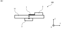
- FIG. 2 is a schematic diagram showing an outline of an antenna device 100 using the multilayer substrate 11 according to embodiment 1.
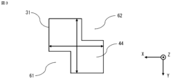
- FIG. 3 is a cross-sectional view showing an outline of a waveguide 31 of the multilayer substrate 11, and is a diagram showing the shape of a cross section perpendicular to the direction in which the waveguide 31 penetrates.
- FIG. 4 is a cross-sectional view showing an outline of another waveguide 31 of the multilayer substrate 11, and is a diagram showing the shape of a cross section perpendicular to the direction in which the waveguide 31 penetrates.
- FIG. 1 is a cross-sectional view showing an outline of a multilayer substrate 11 according to embodiment 1, and is a diagram of the multilayer substrate 11 cut at the A-A cross section position in FIG. 6.
- FIG. 2 is a schematic diagram showing an outline
- FIG. 5 is a cross-sectional view showing an outline of another waveguide 32 of the multilayer substrate 11, and is a diagram showing the shape of a cross section perpendicular to the direction in which the waveguide 32 penetrates.
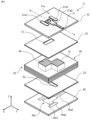
- FIG. 6 is an exploded perspective view showing an outline of the multilayer substrate 11.
- FIG. 7 is a diagram explaining the operation of the waveguide 31 of the multilayer substrate 11.
- FIG. 8 is a diagram showing the transmission line characteristics in the waveguide 31 of the multilayer substrate 11, and is a diagram showing the results of an electromagnetic field analysis of the reflection coefficient.
- the X-axis, Y-axis, and Z-axis shown in the figure are three axes perpendicular to each other.
- the direction parallel to the Y-axis is the first direction
- the direction parallel to the X-axis is the second direction
- the direction parallel to the Z-axis is the third direction, the Z-axis.
- the direction indicated by the arrow in the figure in the X-axis direction is the positive X-direction
- the direction opposite to the positive X-direction is the negative X-direction.
- the antenna device 100 includes a multi-layer substrate 11, a high-frequency signal generator 2, and an antenna 3.
- the multi-layer substrate 11 includes a feeder line 1 that propagates a signal from the high-frequency signal generator 2 to the antenna 3.
- the antenna device 100 using the feeder line 1 is a device that transmits high-frequency signals in the microwave band or millimeter wave band.
- Microwaves have a wavelength of 1 mm to 1 m and a frequency of 300 MHz to 300 GHz.
- Millimeter waves have a wavelength of 1 mm to 10 mm and a frequency of 30 GHz to 300 GHz.
- the antenna device 100 propagates a signal from a first direction to a second direction.
- the high frequency signal generator 2 that generates a high frequency signal is provided, for example, as an IC (Integrated Circuit).
- the power supply line 1 connects the high frequency signal generator 2 and the antenna 3.
- the high frequency signal generator 2 is arranged on the multi-layer board 11, and the antenna 3 is connected to the multi-layer board 11.
- the high frequency signal generator 2 is mounted on a surface of the multi-layer board 11 different from the board surface to which the antenna 3 is connected.
- the antenna 3 is connected to a first conductor layer or a fourth conductor layer, which will be described later.
- the first conductor layer is provided, for example, on one board surface of the multi-layer board 11, and the fourth conductor layer is provided on the other board surface of the multi-layer board 11.
- the high frequency signal generator 2 When the antenna 3 is connected to the first conductor layer, the high frequency signal generator 2 is arranged on the side of the fourth conductor layer, and when the antenna 3 is connected to the fourth conductor layer, the high frequency signal generator 2 is arranged on the side of the first conductor layer.
- the multilayer substrate 11 includes a first dielectric layer 41 having a first conductor layer 21 on one side and a second conductor layer 22 on the other side opposite to the one side, a second dielectric layer 42 having a third conductor layer 23 on one side and a fourth conductor layer 24 on the other side opposite to the one side, in which the third conductor layer 23 is disposed at a distance from the second conductor layer 22, one or more intermediate dielectric layers 43 disposed between the second conductor layer 22 and the third conductor layer 23, and a waveguide 31.
- the intermediate dielectric layer 43 may be either single or multiple.
- the multilayer substrate 11 includes five intermediate dielectric layers 43, which are intermediate dielectric layers 43a, 43b, 43c, 43d, and 43e.
- intermediate conductor layers 25 are provided between the respective intermediate dielectric layers 43.
- four intermediate conductor layers 25a, 25b, 25c, and 25d are provided.
- Each of the conductor layers of the multilayer substrate 11 is, for example, copper foil.
- the first dielectric layer 41, the second dielectric layer 42, and the intermediate dielectric layer 43 are stacked in the Z direction, and the surfaces on which each plate-like layer is stacked are parallel to the X direction and the Y direction.
- the waveguide 31 is a conductive cylindrical member that abuts against the inner circumferential surface of a through hole that penetrates a specific portion of the intermediate dielectric layer 43 in the direction from the second conductor layer 22 to the third conductor layer 23, and the inside of the cylindrical member is filled with a dielectric 44 made of a material different from the first dielectric layer 41, the second dielectric layer 42, and the intermediate dielectric layer 43.
- the material of the first dielectric layer 41, the second dielectric layer 42, and the intermediate dielectric layer 43 is, for example, a glass cloth-based epoxy resin.
- the material of the dielectric 44 filled in the waveguide 31 is, for example, an epoxy resin.
- a low-loss dielectric 44 can be provided on the inside of the waveguide 31.
- the performance of the waveguide 31 can be improved.
- the first conductor pattern 21a is formed on the first conductor layer 21.
- the fourth conductor pattern 24a is formed on the fourth conductor layer 24.
- the power supply line 1 is formed from the first conductor pattern 21a, the fourth conductor pattern 24a, and the waveguide 31.
- the shape of the first conductor pattern 21a in this embodiment will be described.
- the first conductor pattern 21a has a ring-shaped line portion 21a1 having a rectangular opening, and an input/output terminal portion 21a2 extending from the ring-shaped line portion 21a1 in the positive Y direction.
- the shape of the opening is not limited to a rectangle, and may be, for example, a polygon other than a rectangle.
- the input/output terminal portion 21a2 has a multi-step shape whose width changes between the ring-shaped line portion 21a1 and the end of the first dielectric layer 41.
- the first conductor pattern 21a has non-connected portions 21a3 on both sides in the X direction adjacent to the annular line portion 21a1, with a gap between them.
- the shape of the non-connected portions 21a3 is rectangular, but the shape of the non-connected portions 21a3 is not limited to a rectangle and may be, for example, a polygon other than a rectangle.
- the shape of the fourth conductor pattern 24a is the same as that of the first conductor pattern 21a.
- the fourth conductor pattern 24a has a ring-shaped line portion 24a1, an input/output terminal portion 24a2, and a non-connected portion 24a3.
- the extension direction of the input/output terminal portion 24a2 is different from the extension direction of the input/output terminal portion 21a2, and the extension direction of the input/output terminal portion 24a2 is the negative X direction.
- the antenna 3 is connected to an end of the input/output terminal portion 21a2 or the input/output terminal portion 24a2.
- the first conductor pattern 21a is electromagnetically coupled to the second slot 51.
- the opening of the annular line portion 21a1 is arranged to overlap with the second slot 51 when viewed in the Z direction, as shown in FIG. 1.
- the fourth conductor pattern 24a is electromagnetically coupled to the third slot 52.
- the opening of the annular line portion 24a1 is arranged to overlap with the third slot 52 when viewed in the Z direction.
- the shapes of the conductor patterns are not limited to the shapes shown in this embodiment, as long as each conductor pattern has a shape that electromagnetically couples with its respective slot.
- the second conductor layer 22 is formed with a second slot 51, which is an open portion of the second conductor layer 22, as shown in FIG. 6.
- the third conductor layer 23 is formed with a third slot 52, which is an open portion of the third conductor layer 23.
- the second slot 51 is electromagnetically coupled to the first conductor pattern 21a and the waveguide 31. When viewed in the Z direction, the second slot 51 is arranged so as to overlap with the first conductor pattern 21a and the inner portion of the waveguide 31, as shown in FIG. 1.
- the third slot 52 is electromagnetically coupled to the fourth conductor pattern 24a and the waveguide 31. When viewed in the Z direction, the third slot 52 is arranged so as to overlap with the fourth conductor pattern 24a and the inner portion of the waveguide 31.
- the second slot 51 and the third slot 52 are formed in a rectangular shape.
- each slot has a shape that electromagnetically couples with the respective conductor pattern and the waveguide 31, the shape of the slot is not limited to the shape shown in this embodiment.
- the slot may be a polygon other than a square or rectangle, or may have a floating conductor pattern in the inner region of the slot.
- ⁇ Waveguide 31> The configuration of the waveguide 31, which is a main part of the present application, will be described.
- the shape of the cross section of the waveguide 31 perpendicular to the direction of penetration through the intermediate dielectric layer 43 is a rectangle with both corners on one diagonal line cut out.
- the cut-out parts are called cut-out parts 61 and 62.
- the shape of the cut-out parts of the cross section of the waveguide 31 perpendicular to the direction of penetration through the intermediate dielectric layer 43 shown in FIG. 3 is a rectangle.
- the cut-out parts 61 and 62 may be square or rectangular as shown in FIG. 4.
- the cut-out parts 61 and 62 are arranged symmetrically with respect to the diagonal line opposite to the diagonal line where the cut-outs are provided.
- the cross-sectional quadrangle of the waveguide 31 is a square and the cutouts 61 and 62 are rectangular, the cutouts 61 and 62 are arranged asymmetrically with respect to the diagonal line opposite to the diagonal line where the cutouts are provided.
- the shape of the waveguide 31 can be easily designed according to the matching conditions of the transmission line characteristics propagating through the waveguide 31, because the shape of the cutout is simple.
- the shape of the cutout is not limited to a rectangle, and can be, for example, a polygon other than a rectangle, or a cutout shape that is asymmetrical, according to the matching conditions of the transmission line characteristics.
- the shape of the cutout is other than a rectangle, the number of design parameters increases, making it possible to design a waveguide 31 with more precise transmission characteristics.
- the corners of the rectangular cross section of the waveguide 31 are right angles or rounded.
- the corners of the rectangular cross section of the waveguide 31 shown in FIG. 3 of this embodiment are right angles. When the corners are right angles, the desired transmission characteristics can be easily obtained in the waveguide 31.
- the corners of the rectangular cross section of the waveguide 31 are not limited to right angles.
- the corners of the rectangular cross section of the waveguide 31 may be rounded depending on, for example, the manufacturing conditions of the waveguide 32 or the matching conditions of the transmission line characteristics.
- the other waveguide 32 has cutouts 63 and 64. When the corners are rounded, the manufacturability of the waveguide 32 is improved, and the productivity of the multilayer board 11 can be improved.
- FIG. 7(a) to 7(c) The operation of the waveguide 31 with the cutouts 61, 62 will be explained using Figures 7(a) to 7(c).
- the arrows shown in Figures 7(a) to 7(c) indicate the direction of the electric field excited in the second slot 51, the waveguide 31, and the third slot 52, respectively.
- the signal propagates in the negative Y direction of the first conductor pattern 21a, and then propagates in the negative X direction of the fourth conductor pattern 24a via the waveguide 31.
- the location where the electric field is excited is shown by a solid line
- the location where the electric field is excited thereafter is shown by a dashed line
- other locations are shown by dotted lines.
- the signal propagating in the negative Y direction of the first conductor pattern 21a is electromagnetically coupled to the second slot 51 as shown in FIG. 7(a), and an electric field is excited in the second slot 51 in the negative Y direction (perpendicular to the X axis).
- the signal electromagnetically coupled to the second slot 51 propagates through the waveguide 31 as shown in FIG. 7(b).
- the signal propagating through the waveguide 31 propagates while rotating 45 degrees with respect to the X axis according to the shape of the waveguide 31. Then, the signal rotated 45 degrees with respect to the X axis direction is electromagnetically coupled to the third slot 52 as shown in FIG. 7(c).
- the signal electromagnetically coupled to the third slot 52 propagates while further rotating 45 degrees with respect to the X axis according to the opening shape of the third slot 52.
- the electric field direction of the signal propagating through the third slot 52 is rotated 90 degrees with respect to the electric field direction of the signal propagating through the second slot 51, and finally, it is electromagnetically coupled to the fourth conductor pattern 24a and propagates in the negative X direction.
- the shape of the cross section perpendicular to the direction of penetrating the intermediate dielectric layer 43 in the waveguide 31 is a shape in which both corners on one diagonal line of a rectangle are cut out, so that the signal propagation direction can be changed by 90 degrees inside the multilayer substrate 11. Since the signal propagation direction can be changed by 90 degrees inside the multilayer substrate 11, an additional conductor pattern for changing the signal propagation direction is not required in either the first conductor layer 21 in which the first conductor pattern 21a is provided or the fourth conductor layer 24 in which the fourth conductor pattern 24a is provided. Since an additional conductor pattern is not required, the multilayer substrate 11 can be made smaller.
- the design freedom of the multilayer substrate 11 can be improved. Furthermore, since no discontinuity that abruptly changes the signal propagation direction occurs, the amount of unnecessary radiation can be suppressed. Furthermore, by using such a multilayer substrate 11 in the antenna device 100, the amount of unnecessary radiation can be suppressed, and an antenna device 100 that is smaller in size and has improved design freedom can be obtained.
- FIG. 8 is a diagram showing the reflection coefficient versus normalized frequency obtained by electromagnetic field analysis, with the horizontal axis representing normalized frequency and the vertical axis representing reflection coefficient.
- the reflection coefficient is -20 dB or less at a bandwidth of 8% or more, with the normalized frequency "1" at the center, and that good characteristics are realized.
- This characteristic means that the transmitted frequency propagates without reflection, and the structure of the waveguide 31 disclosed in this application makes it possible to change the signal propagation direction by 90 degrees with good characteristics.
- FIG. 8 shows the analysis results for the waveguide 31 having the vertical cross section shown in FIG. 3, the effectiveness of the structure of the waveguide 31 is the same for the other shapes of the waveguide 31 shown in embodiment 1 and other embodiments described later.
- the dimensions of the waveguide 31 will be described.
- the length of the intermediate dielectric layer 43 in the penetrating direction of the waveguide 31 is a quarter wavelength of the wavelength of the signal propagating through the waveguide 31.
- the direction of the signal propagating through the waveguide 31 is the plus Z direction or the minus Z direction.
- the wavelength of the signal propagating through the waveguide 31 is not limited to a quarter wavelength of the wavelength of the signal propagating through the waveguide 31, and may be changed according to preferred transmission line characteristics or design specifications.
- the length of the intermediate dielectric layer 43 in the penetrating direction of the waveguide 31 is a quarter wavelength of the wavelength of the signal propagating through the waveguide 31, the desired transmission characteristics can be easily obtained in the waveguide 31.
- the guide wavelength is calculated to be 2.25 mm.
- the length of a quarter of the guide wavelength is 0.56 mm.
- the waveguide 31 is provided in the multilayer substrate 11 so that the length of the waveguide 31 in the penetration direction in the intermediate dielectric layer 43 is 0.56 mm. If the length of the waveguide 31 in the penetration direction is 0.56 mm, the thickness of the multilayer substrate 11 is, for example, 1.1 mm.
- the distance between the opposing sides of the rectangular cross section of the waveguide 31 is half the wavelength of the signal propagating through the waveguide 31.
- the distance between the opposing sides of the rectangular cross section of the waveguide 31 is the distance indicated by the arrow.
- the distance between the opposing sides of the rectangular cross section of the waveguide 31 is not limited to half the wavelength of the signal propagating through the waveguide 31, and the length may be changed depending on the preferred transmission line characteristics or design specifications.
- the distance between the opposing sides of the rectangular cross section of the waveguide 31 is half the wavelength of the signal propagating through the waveguide 31, the desired transmission characteristics can be easily obtained in the waveguide 31.
- ⁇ Formation of Waveguide 31> An example of a method for forming the waveguide 31 will be described with reference to the waveguide 31 shown in FIG. 1.
- a through hole penetrating a specific portion of the intermediate dielectric layer 43 is formed by a drill.
- the inner circumferential surface of the through hole is plated to form a conductive tubular member.
- the plating material is, for example, copper.
- the conductive tubular member and the intermediate conductor layer 25 are electrically connected.
- the inside of the tubular member is filled with a dielectric 44 made of a material different from the first dielectric layer 41, the second dielectric layer 42, and the intermediate dielectric layer 43.
- the material of the dielectric 44 to be filled is, for example, epoxy resin.
- the waveguide 31 portion of the multilayer substrate 11 is formed.
- the second conductor layer 22, the third conductor layer 23, the first dielectric layer 41, the second dielectric layer 42, the first conductor layer 21, and the fourth conductor layer 24 are stacked and provided.
- a first conductor pattern 21 a is provided on the first conductor layer 21
- a fourth conductor pattern 24 a is provided on the fourth conductor layer 24 , thereby forming the multilayer substrate 11 .
- the multilayer substrate 11 comprises a first dielectric layer 41 having a first conductor layer 21 on one side and a second conductor layer 22 on the other side, a second dielectric layer 42 having a third conductor layer 23 on one side and a fourth conductor layer 24 on the other side, in which the third conductor layer 23 is disposed at a distance from the second conductor layer 22, one or more intermediate dielectric layers 43 disposed between the second conductor layer 22 and the third conductor layer 23, and a conductive tubular member abutting against the inner circumferential surface of a through hole penetrating a specific portion of the intermediate dielectric layer 43, and a conductive tubular member disposed on the inside of the tubular member.
- the waveguide 31 is filled with a dielectric 44 made of a material different from the first dielectric layer 41, the second dielectric layer 42, and the intermediate dielectric layer 43.
- the cross-sectional shape of the waveguide 31 perpendicular to the direction of penetration through the intermediate dielectric layer 43 is a rectangle with both corners on one diagonal line cut out, so that the signal propagation direction can be changed by 90 degrees inside the multilayer substrate 11, and therefore an additional conductor pattern for changing the signal propagation direction in either the first conductor layer 21 or the fourth conductor layer 24 is not required. Since an additional conductor pattern is not required, the multilayer substrate 11 can be made smaller. Furthermore, since an additional conductor pattern is not required and the area of the circuit does not increase, the design freedom of the multilayer substrate 11 can be improved. Furthermore, since no discontinuity that abruptly changes the signal propagation direction occurs, the amount of unnecessary radiation in the multilayer substrate 11 can be suppressed.
- the length of the intermediate dielectric layer 43 in the direction through which the waveguide 31 penetrates is a quarter of the wavelength of the signal propagating through the waveguide 31, the desired transmission characteristics can be easily obtained in the waveguide 31. Also, if the distance between opposing sides of the rectangular cross section of the waveguide 31 is a half of the wavelength of the signal propagating through the waveguide 31, the desired transmission characteristics can be easily obtained in the waveguide 31.
- the desired transmission characteristics can be easily obtained in the waveguide 31. If the corners of the rectangular cross section of the waveguide 31 are rounded, the desired transmission characteristics can be easily obtained and the manufacturability of the waveguide 31 is improved, thereby improving the productivity of the multilayer board 11.
- the shape of the cutout portion of the waveguide 31 in a cross section perpendicular to the direction of penetration through the intermediate dielectric layer 43 is rectangular, the shape of the cutout is simple, so the shape of the waveguide 31 can be easily designed according to the matching conditions of the transmission line characteristics propagating through the waveguide 31. Furthermore, when the shape of the cutout portions 61, 62 is other than rectangular, the number of design parameters increases, making it possible to design a waveguide 31 with more precise transmission characteristics.
- the antenna device 100 includes the multilayer substrate 11 disclosed in the present application and the antenna 3 connected to the first conductor layer 21 or the fourth conductor layer 24, the use of the multilayer substrate 11 disclosed in the present application in the antenna device 100 makes it possible to obtain an antenna device 100 that is smaller in size and has improved design freedom while suppressing the amount of unwanted radiation.
- FIG. 9 is a cross-sectional view showing an outline of the multilayer substrate 12 according to the second embodiment, and shows the multilayer substrate 12 cut at the same position as the A-A cross-sectional position in Fig. 6.
- Fig. 10 is a cross-sectional view of the multilayer substrate 12 cut at the B-B cross-sectional position in Fig. 9, showing a cross-sectional view of the intermediate dielectric layer 43c.
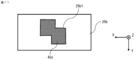
- Fig. 11 is a cross-sectional view of the multilayer substrate 12 cut at the C-C cross-sectional position in Fig. 9, showing a cross-sectional view of the intermediate conductor layer 25b.
- the multilayer substrate 12 according to the second embodiment has a configuration in which a waveguide 33 is formed by a plurality of via holes 71.
- the multilayer substrate 11 includes a first dielectric layer 41 having a first conductor layer 21 on one side and a second conductor layer 22 on the other side opposite the first side, a second dielectric layer 42 having a third conductor layer 23 on one side and a fourth conductor layer 24 on the other side opposite the first side, in which the third conductor layer 23 is disposed at a distance from the second conductor layer 22, one or more intermediate dielectric layers 43 disposed between the second conductor layer 22 and the third conductor layer 23, and a plurality of via holes 71 penetrating the intermediate dielectric layer 43 in the direction from the second conductor layer 22 to the third conductor layer 23 and surrounding a specific portion of the intermediate dielectric layer 43.
- the intermediate dielectric layer 43 may be single or multiple.
- the multilayer substrate 11 has five intermediate dielectric layers 43, that is, intermediate dielectric layers 43a, 43b, 43c, 43d, and 43e.
- intermediate conductor layers 25 are provided at least in the portions between the plurality of intermediate dielectric layers 43 excluding the waveguide 33 consisting of the plurality of via holes 71 and specific portions.
- four intermediate conductor layers 25a, 25b, 25c, and 25d are provided.
- Each of the conductor layers of the multilayer substrate 11 is, for example, copper foil.
- a waveguide 33 is formed by a plurality of via holes 71.
- the shape of the line connecting the plurality of via holes 71 in a cross section perpendicular to the direction of penetration of the intermediate dielectric layer 43 in the waveguide 33 is a shape in which both corners on one diagonal of a rectangle are cut out.
- the cut-out portions are called cut-out portions 65 and 66.
- the intermediate conductor layer 25b has an opening 25b1 surrounding a specific portion of the intermediate dielectric layer 43.
- the portion of the intermediate dielectric layer 43 shown in FIG. 11 is a portion of the intermediate dielectric layer 43c.
- the intermediate conductor layers 25a, 25c, and 25d have the same configuration as the intermediate conductor layer 25b.
- the plurality of via holes 71 are provided so as to overlap the periphery of the opening 25b1 surrounding the specific portion of the intermediate dielectric layer 43.
- the plurality of via holes 71 and the intermediate conductor layer 25 are electrically connected.
- the waveguide 33 is formed by 20 via holes 71, but the number of via holes 71 is not limited to this.
- the waveguide 33 formed by the multiple via holes 71 has a shape in which the line connecting the multiple via holes 71 in a vertical cross section has a shape in which both corners on one diagonal of a rectangle are cut out, so that the signal propagation direction can be changed by 90 degrees inside the multilayer substrate 12, similar to the waveguide 31 of the first embodiment. Since the signal propagation direction can be changed by 90 degrees inside the multilayer substrate 11, an additional conductor pattern for changing the signal propagation direction is not required in either the first conductor layer 21 on which the first conductor pattern 21a is provided or the fourth conductor layer 24 on which the fourth conductor pattern 24a is provided. Since an additional conductor pattern is not required, the multilayer substrate 12 can be made smaller. Furthermore, since an additional conductor pattern is not required and the area of the circuit does not increase, the design freedom of the multilayer substrate 12 can be improved. Furthermore, since no discontinuity that abruptly changes the signal propagation direction occurs, the amount of unnecessary radiation can be suppressed.
- the shape of the waveguide 31 depended on the size of the drill used to form the through holes, particularly in corners such as the corners of the waveguide 31.
- the waveguide 33 is formed by multiple via holes 71, so the shape of the waveguide 33 does not depend on the size of the drill, improving the design freedom for the shape of the waveguide 33.
- the multilayer substrate 12 includes a plurality of via holes 71 that penetrate the intermediate dielectric layer 43 in the direction from the second conductor layer 22 to the third conductor layer 23 and surround a specific portion of the intermediate dielectric layer 43, and the plurality of via holes 71 form a waveguide 33.
- the shape of the line connecting the plurality of via holes 71 in a cross section perpendicular to the direction of penetration of the intermediate dielectric layer 43 in the waveguide 33 is a shape in which both corners on one diagonal line of a rectangle are cut out, so that the signal propagation direction can be changed by 90 degrees inside the multilayer substrate 11, and therefore an additional conductor pattern for changing the signal propagation direction is not required in either the first conductor layer 21 or the fourth conductor layer 24.
- the waveguide 33 is formed by a plurality of via holes 71, the design freedom for the shape of the waveguide 33 can be improved. In addition, since no discontinuity that abruptly changes the signal propagation direction occurs, the amount of unnecessary radiation can be suppressed.
Landscapes
- Waveguides (AREA)
Abstract
多層基板(11)は一方の側に第一導体層(21)及び他方の側に第二導体層(22)を有した第一の誘電体層(41)、一方の側に第三導体層(23)及び他方の側に第四導体層(24)を有し、第二導体層(22)と間隔を空けて第三導体層(23)が配置された第二の誘電体層(42)、第二導体層(22)と第三導体層(23)の間に配置された単数又は複数の中間誘電体層(43)、第二導体層(22)から第三導体層(23)の方向に中間誘電体層(43)の特定の部分を貫通した貫通孔の内周面に当接した導電性の筒状部材であって、筒状部材の内側に第一の誘電体層(41)、第二の誘電体層(42)、および中間誘電体層(43)と異なる材料からなる誘電体(44)が充填された導波管(31)を備え、導波管(31)の中間誘電体層(43)を貫通した方向に対して垂直な断面の形状は四角形の1つの対角線上の角部の双方が切り欠かれた形状である。
Description
本願は、多層基板及びそれを用いたアンテナ装置に関するものである。
アンテナ装置は、マイクロ波帯あるいはミリ波帯の高周波信号を伝送する装置である。アンテナ装置は、アンテナと、高周波信号を発生させる高周波信号発生器であるIC(Integrated Circuit)と、給電線路とを備える。給電線路は、アンテナとICとを接続する。ICは、アンテナ及び給電線路が形成された誘電体基板の基板面と異なる基板面に実装される場合がある。
ICをアンテナが形成された誘電体基板の基板面と異なる面に実装する場合、双方の面を接続するための回路(変換器)が必要である。誘電体基板である多層基板の内層に、誘電体を充填した導波管を形成した構成が開示されている(例えば、特許文献1参照)。特許文献1では、変換器は、多層基板と、多層基板の内層に形成され、誘電体を充填した導波管と、マイクロストリップ線路とを有し、導波管からマイクロストリップ線路へ信号は伝搬する。開示された変換器を用いれば、多層基板の表面と裏面とを接続することができる。
多層基板の内層に形成され、誘電体を充填した導波管を用いることで、多層基板の表面と裏面とを接続することができる。しかしながら、開示された導波管の形状により多層基板の表面と裏面とを接続する場合、伝搬させる信号の方向は、一つの特定の方向に限られている。例えば、表面に設けられ、一つの特定の方向であるX方向に延出したマイクロストリップ線路を伝搬した信号は、導波管を介して、裏面に設けられ、X方向に延出したマイクロストリップ線路のみを伝搬することになる。そのため、信号の伝搬方向を表面と裏面とで90度、つまり垂直方向に転換させたい場合、表面、又は裏面のどちらか一方の面に信号の伝搬方向を変えるための追加の給電線路が必要となる。
追加の給電線路において、例えば、給電線路を引き回せるスペースの確保が十分できない場合、信号の伝搬方向を急激に変えなければならない。信号の伝搬方向を急激に変えた給電線路では、不連続部が発生することになる。不連続部では、不要な電波が放射(以下、不要放射と称する)される。不要放射は、その量によって、アンテナ性能及び回路性能に影響を与える。そのため、不連続部から不要放射が発生するという課題があった。不要放射の量を抑制するためには、追加の給電線路において緩慢に線路の方向を転換すればよい。しかしながら、追加の給電線路の方向を緩慢に転換した場合、給電線路を引き回すスペースが増大するので、給電線路を設けた回路の面積が増大し、多層基板が大型化するという課題があった。また、回路の面積が増大するため、多層基板の設計の自由度が低減するという課題があった。
そこで、本願は、不要放射の量を抑制すると共に、小型化及び設計自由度が向上した多層基板、及びそれを用いたアンテナ装置を得ることを目的とする。
本願に開示される多層基板は、一方の側に第一導体層、及び前記一方の側とは反対側の他方の側に第二導体層を有した第一の誘電体層と、一方の側に第三導体層、及び前記一方の側とは反対側の他方の側に第四導体層を有し、前記第二導体層と間隔を空けて前記第三導体層が配置された第二の誘電体層と、前記第二導体層と前記第三導体層との間に配置された単数又は複数の中間誘電体層と、前記第二導体層から前記第三導体層の方向に前記中間誘電体層の特定の部分を貫通した貫通孔の内周面に当接した導電性の筒状部材であって、前記筒状部材の内側に前記第一の誘電体層、前記第二の誘電体層、及び前記中間誘電体層とは異なる材料からなる誘電体が充填された導波管とを備え、複数の前記中間誘電体層を有した場合、複数の前記中間誘電体層のそれぞれの間の部分には、中間導体層が設けられ、前記導波管における前記中間誘電体層を貫通した方向に対して垂直な断面の形状は、四角形の1つの対角線上の角部の双方が切り欠かれた形状である。
本願に開示されるアンテナ装置は、本願に開示された多層基板と、前記第一導体層又は前記第四導体層に形成されたアンテナと、を備えたものである。
本願に開示される多層基板によれば、一方の側に第一導体層、及び一方の側とは反対側の他方の側に第二導体層を有した第一の誘電体層と、一方の側に第三導体層、及び一方の側とは反対側の他方の側に第四導体層を有し、第二導体層と間隔を空けて第三導体層が配置された第二の誘電体層と、第二導体層と第三導体層との間に配置された単数又は複数の中間誘電体層と、中間誘電体層の特定の部分を貫通した貫通孔の内周面に当接した導電性の筒状部材であって、筒状部材の内側に第一の誘電体層、第二の誘電体層、及び中間誘電体層とは異なる材料からなる誘電体が充填された導波管とを備え、導波管における中間誘電体層を貫通した方向に対して垂直な断面の形状が、四角形の1つの対角線上の角部の双方が切り欠かれた形状であるため、多層基板の内側において信号の伝搬する方向を90度変えることができるので、第一導体層又は第四導体層のどちらか一方の層において信号の伝搬方向を変えるための追加の導体パターンが不要になる。追加の導体パターンが不要になるので、多層基板を小型化することができる。また、追加の導体パターンが不要になり回路の面積が増大しないので、多層基板の設計自由度を向上させることができる。また、信号の伝搬方向を急激に変える不連続部が発生しないので、多層基板における不要放射の量を抑制することができる。
本願に開示されるアンテナ装置によれば、本願に開示された多層基板と、第一導体層又は第四導体層に接続されたアンテナと、を備えたため、本願に開示した多層基板をアンテナ装置に用いることで、不要放射の量を抑制すると共に、小型化及び設計自由度が向上したアンテナ装置を得ることができる。
以下、本願の実施の形態による多層基板及びそれを用いたアンテナ装置を図に基づいて説明する。なお、各図において同一、または相当部材、部位については同一符号を付して説明する。
実施の形態1.
図1は実施の形態1に係る多層基板11の概略を示す断面図で、図6のA-A断面位置で多層基板11を切断した図、図2は実施の形態1に係る多層基板11を用いたアンテナ装置100の概略を示す模式図、図3は多層基板11の導波管31の概略を示す断面図で、導波管31の貫通した方向に対して垂直な断面の形状を示した図、図4は多層基板11の別の導波管31の概略を示す断面図で、導波管31の貫通した方向に対して垂直な断面の形状を示した図、図5は多層基板11の別の導波管32の概略を示す断面図で、導波管32の貫通した方向に対して垂直な断面の形状を示した図、図6は多層基板11の概略を示す分解斜視図、図7は多層基板11の導波管31の動作を説明する図、図8は多層基板11の導波管31における伝送線路特性を示す図で、反射係数の電磁界解析の結果を示した図である。なお、図中に記載するX軸、Y軸及びZ軸は、互いに垂直な3軸とする。Y軸に平行な方向を第1の方向であるY軸方向、X軸に平行な方向を第2の方向であるX軸方向、Z軸に平行な方向を第3の方向であるZ軸方向とする。X軸方向のうち図中矢印で示す方向をプラスX方向、プラスX方向の逆の方向をマイナスX方向とし、Y軸方向及びZ軸方向についてもX軸方向の場合と同様とする。
図1は実施の形態1に係る多層基板11の概略を示す断面図で、図6のA-A断面位置で多層基板11を切断した図、図2は実施の形態1に係る多層基板11を用いたアンテナ装置100の概略を示す模式図、図3は多層基板11の導波管31の概略を示す断面図で、導波管31の貫通した方向に対して垂直な断面の形状を示した図、図4は多層基板11の別の導波管31の概略を示す断面図で、導波管31の貫通した方向に対して垂直な断面の形状を示した図、図5は多層基板11の別の導波管32の概略を示す断面図で、導波管32の貫通した方向に対して垂直な断面の形状を示した図、図6は多層基板11の概略を示す分解斜視図、図7は多層基板11の導波管31の動作を説明する図、図8は多層基板11の導波管31における伝送線路特性を示す図で、反射係数の電磁界解析の結果を示した図である。なお、図中に記載するX軸、Y軸及びZ軸は、互いに垂直な3軸とする。Y軸に平行な方向を第1の方向であるY軸方向、X軸に平行な方向を第2の方向であるX軸方向、Z軸に平行な方向を第3の方向であるZ軸方向とする。X軸方向のうち図中矢印で示す方向をプラスX方向、プラスX方向の逆の方向をマイナスX方向とし、Y軸方向及びZ軸方向についてもX軸方向の場合と同様とする。
<アンテナ装置100>
アンテナ装置100は、図2に示すように、多層基板11と、高周波信号発生器2と、アンテナ3とを備える。多層基板11は、高周波信号発生器2からアンテナ3に信号を伝搬する給電線路1を備える。給電線路1を用いたアンテナ装置100は、マイクロ波帯あるいはミリ波帯の高周波信号を伝送する装置である。マイクロ波は波長が1mmから1m、周波数が300MHzから300GHzである。ミリ波は波長が1mmから10mm、周波数が30GHzから300GHzである。アンテナ装置100は、信号を第1の方向から第2の方向に伝搬させる。
アンテナ装置100は、図2に示すように、多層基板11と、高周波信号発生器2と、アンテナ3とを備える。多層基板11は、高周波信号発生器2からアンテナ3に信号を伝搬する給電線路1を備える。給電線路1を用いたアンテナ装置100は、マイクロ波帯あるいはミリ波帯の高周波信号を伝送する装置である。マイクロ波は波長が1mmから1m、周波数が300MHzから300GHzである。ミリ波は波長が1mmから10mm、周波数が30GHzから300GHzである。アンテナ装置100は、信号を第1の方向から第2の方向に伝搬させる。
高周波信号を発生させる高周波信号発生器2は、例えば、IC(Integrated Circuit)で設けられる。給電線路1は、高周波信号発生器2とアンテナ3とを接続する。多層基板11に高周波信号発生器2が配置されると共に、多層基板11にアンテナ3が接続される。高周波信号発生器2は、アンテナ3が接続された多層基板11の基板面と異なる面に実装される。アンテナ3は、後述する第一導体層又は第四導体層に接続される。第一導体層は、例えば、多層基板11の一方の基板面に設けられ、第四導体層は多層基板11の他方の基板面に設けられる。アンテナ3が第一導体層に接続された場合、高周波信号発生器2は第四導体層の側に配置され、アンテナ3が第四導体層に接続された場合、高周波信号発生器2は第一導体層の側に配置される。
<多層基板11>
多層基板11は、図1に示すように、一方の側に第一導体層21、及び一方の側とは反対側の他方の側に第二導体層22を有した第一の誘電体層41と、一方の側に第三導体層23、及び一方の側とは反対側の他方の側に第四導体層24を有し、第二導体層22と間隔を空けて第三導体層23が配置された第二の誘電体層42と、第二導体層22と第三導体層23との間に配置された単数又は複数の中間誘電体層43と、導波管31とを備える。中間誘電体層43は、単数でも複数でも構わない。本実施の形態では、多層基板11は、5つの中間誘電体層43として、中間誘電体層43a、43b、43c、43d、43eを有する。多層基板11が複数の中間誘電体層43を有した場合、複数の中間誘電体層43のそれぞれの間の部分には、中間導体層25が設けられる。本実施の形態では、多層基板11が5つの中間誘電体層43を有するため、4つの中間導体層25a、25b、25c、25dが設けられる。多層基板11が有した導体層のそれぞれは、例えば、銅箔である。図1では、第一の誘電体層41、第二の誘電体層42、及び中間誘電体層43はZ方向に積層され、板状のそれぞれの層が積層される面は、X方向及びY方向に平行である。
多層基板11は、図1に示すように、一方の側に第一導体層21、及び一方の側とは反対側の他方の側に第二導体層22を有した第一の誘電体層41と、一方の側に第三導体層23、及び一方の側とは反対側の他方の側に第四導体層24を有し、第二導体層22と間隔を空けて第三導体層23が配置された第二の誘電体層42と、第二導体層22と第三導体層23との間に配置された単数又は複数の中間誘電体層43と、導波管31とを備える。中間誘電体層43は、単数でも複数でも構わない。本実施の形態では、多層基板11は、5つの中間誘電体層43として、中間誘電体層43a、43b、43c、43d、43eを有する。多層基板11が複数の中間誘電体層43を有した場合、複数の中間誘電体層43のそれぞれの間の部分には、中間導体層25が設けられる。本実施の形態では、多層基板11が5つの中間誘電体層43を有するため、4つの中間導体層25a、25b、25c、25dが設けられる。多層基板11が有した導体層のそれぞれは、例えば、銅箔である。図1では、第一の誘電体層41、第二の誘電体層42、及び中間誘電体層43はZ方向に積層され、板状のそれぞれの層が積層される面は、X方向及びY方向に平行である。
導波管31は、第二導体層22から第三導体層23の方向に中間誘電体層43の特定の部分を貫通した貫通孔の内周面に当接した導電性の筒状部材であって、筒状部材の内側に第一の誘電体層41、第二の誘電体層42、及び中間誘電体層43とは異なる材料からなる誘電体44が充填されている。第一の誘電体層41、第二の誘電体層42、及び中間誘電体層43の材料は、例えば、ガラス布基材エポキシ樹脂である。導波管31に充填された誘電体44の材料は、例えば、エポキシ樹脂である。導波管31の内側の誘電体44と誘電体層とで異なる誘電体にすることで、導波管31の内側に低損失な誘電体44を設けることができる。導波管31の内側に低損失な誘電体44を設けることで、導波管31の性能を向上させることができる。
第一導体層21には、図6に示すように、第一導体パターン21aが形成される。第四導体層24には、第四導体パターン24aが形成される。図6では、第四導体パターン24aは外形のみを破線で示す。本実施の形態では、給電線路1は、第一導体パターン21aと、第四導体パターン24aと、導波管31とから形成される。本実施の形態における第一導体パターン21aの形状について説明する。第一導体パターン21aは、矩形の開口部を有した環状線路部21a1と、環状線路部21a1からプラスY方向に延出した入出力端子部21a2とを有する。開口部の形状は矩形に限るものではなく、例えば、矩形以外の多角形であっても構わない。入出力端子部21a2は、環状線路部21a1と第一の誘電体層41の端部との間の部分で幅の変わる多段形状を有している。第一導体パターン21aは、X方向の両側であって、環状線路部21a1に隣接した位置に、環状線路部21a1とは隙間を空けて配置された非接続部21a3を有する。本実施の形態では、非接続部21a3の形状は矩形であるが、非接続部21a3の形状は矩形に限るものではなく、例えば、矩形以外の多角形であっても構わない。
第四導体パターン24aの形状は、第一導体パターン21aの形状と同様である。第四導体パターン24aは、環状線路部24a1と、入出力端子部24a2と、非接続部24a3とを有する。ただし、入出力端子部24a2の延出方向が入出力端子部21a2の延出方向とは異なっており、入出力端子部24a2の延出方向は、マイナスX方向である。アンテナ3は、入出力端子部21a2又は入出力端子部24a2の端部に接続される。
第一導体パターン21aは、第二スロット51と電磁界結合する。環状線路部21a1の開口部は、Z方向に見て、図1に示すように、第二スロット51と重複して配置されている。第四導体パターン24aは、第三スロット52と電磁界結合する。環状線路部24a1の開口部は、Z方向に見て、第三スロット52と重複して配置されている。それぞれの導体パターンがそれぞれのスロットと電磁界結合する形状であれば、導体パターンの形状は、本実施の形態に示した形状に限るものではない。
第二導体層22には、図6に示すように、第二導体層22の開口した部分である第二スロット51が形成される。第三導体層23には、第三導体層23の開口した部分である第三スロット52が形成される。第二スロット51は、第一導体パターン21a及び導波管31と電磁界結合する。第二スロット51は、Z方向に見て、図1に示すように、第一導体パターン21a及び導波管31の内側部分と重複して配置されている。第三スロット52は、第四導体パターン24a及び導波管31と電磁界結合する。第三スロット52は、Z方向に見て、第四導体パターン24a及び導波管31の内側部分と重複して配置されている。
本実施の形態では、第二スロット51及び第三スロット52は、長方形に形成される。それぞれのスロットがそれぞれの導体パターン及び導波管31と電磁界結合する形状であれば、スロットの形状は、本実施の形態に示した形状に限るものではない。スロットは、形状が正方形又は矩形以外の多角形、又はスロットの内側の領域に浮遊導体パターンを有した構成であっても構わない。
<導波管31>
本願の要部である導波管31の構成について説明する。導波管31における中間誘電体層43を貫通した方向に対して垂直な断面の形状は、四角形の1つの対角線上の角部の双方が切り欠かれた形状である。切り欠かれた部分を、切欠き部61、62と称する。図3に示した導波管31における中間誘電体層43を貫通した方向に対して垂直な断面の切り欠かれた部分の形状は、四角形である。切欠き部61、62の形状は、正方形でもよく、図4に示すように、長方形であっても構わない。導波管31の断面の四角形が正方形であり、切欠き部61、62が正方形の場合、切り欠きを設けた対角線とは反対側の対角線に対して切欠き部61、62は対称に配置される。導波管31の断面の四角形が正方形であり、切欠き部61、62が長方形の場合、切り欠きを設けた対角線とは反対側の対角線に対して切欠き部61、62は非対称に配置される。
本願の要部である導波管31の構成について説明する。導波管31における中間誘電体層43を貫通した方向に対して垂直な断面の形状は、四角形の1つの対角線上の角部の双方が切り欠かれた形状である。切り欠かれた部分を、切欠き部61、62と称する。図3に示した導波管31における中間誘電体層43を貫通した方向に対して垂直な断面の切り欠かれた部分の形状は、四角形である。切欠き部61、62の形状は、正方形でもよく、図4に示すように、長方形であっても構わない。導波管31の断面の四角形が正方形であり、切欠き部61、62が正方形の場合、切り欠きを設けた対角線とは反対側の対角線に対して切欠き部61、62は対称に配置される。導波管31の断面の四角形が正方形であり、切欠き部61、62が長方形の場合、切り欠きを設けた対角線とは反対側の対角線に対して切欠き部61、62は非対称に配置される。
切欠き部の形状を四角形とした場合、切り欠きの形状が単純な形状であるため、導波管31を伝搬する伝送線路特性の整合条件に応じて、導波管31の形状の設計を容易に行うことができる。切欠き部の形状は四角形に限るものではなく、伝送線路特性の整合条件に応じて、例えば、四角形以外の多角形、又は左右が非対称な切り欠き形状でも構わない。切欠き部の形状を四角形以外にした場合、設計のパラメータが増えるため、より精密な伝送特性を備えた導波管31を設計することができる。
導波管31の断面の四角形における角部は、直角である、又は丸みを帯びた形状である。本実施の形態の図3に示した導波管31の断面の四角形における角部は、直角である。角部が直角である場合、導波管31において、所望の伝送特性を容易に得ることができる。導波管31の断面の四角形における角部は、直角に限るものではない。図5に示した別の導波管32の例のように、導波管31の断面の四角形における角部は、例えば、導波管32の製造条件、又は伝送線路特性の整合条件に応じて、丸みを帯びた形状であっても構わない。別の導波管32は、切欠き部63、64を有する。角部が丸みを帯びた形状である場合、導波管32の製造性が向上するため、多層基板11の生産性を向上させることができる。
切欠き部61、62を設けた導波管31の動作について、図7(a)から図7(c)を用いて説明する。図7(a)から図7(c)に示した矢印は、第二スロット51、導波管31、第三スロット52のそれぞれに励起される電界方向を示す。ここでは、信号が第一導体パターン21aのマイナスY方向に伝搬した後、導波管31を経由して、第四導体パターン24aのマイナスX方向に伝搬すると仮定して説明する。図において、電界が励起された箇所を実線で示し、その後に電界が励起される箇所を破線で示し、他の箇所を点線で示す。
第一導体パターン21aのマイナスY方向に伝搬する信号は、図7(a)に示すように、第二スロット51に電磁結合し、第二スロット51にマイナスY方向(X軸に対して垂直な方向)に電界が励起する。第二スロット51に電磁結合した信号は、図7(b)に示すように、導波管31を伝搬する。導波管31を伝搬する信号は、導波管31の形状に応じて、X軸に対して45度回転して伝搬する。その後、X軸方向に対して45度に回転した信号は、図7(c)に示すように、第三スロット52に電磁結合する。第三スロット52に電磁結合する信号は、第三スロット52の開口形状に応じて、さらにX軸に対して45度回転して伝搬する。第三スロット52を伝搬する信号の電界方向は、第二スロット51を伝搬した信号の電界方向に対して90度回転した状態となり、最終的に、第四導体パターン24aに電磁結合して、マイナスX方向に伝搬する。
このように導波管31における中間誘電体層43を貫通した方向に対して垂直な断面の形状を、四角形の1つの対角線上の角部の双方が切り欠かれた形状にしたため、多層基板11の内側において信号の伝搬する方向を90度変えることができる。多層基板11の内側において信号の伝搬する方向を90度変えることができるので、第一導体パターン21aを設けた第一導体層21、又は第四導体パターン24aを設けた第四導体層24のどちらか一方の層において信号の伝搬方向を変えるための追加の導体パターンが不要になる。追加の導体パターンが不要になるので、多層基板11を小型化することができる。また、追加の導体パターンが不要になり回路の面積が増大しないので、多層基板11の設計自由度を向上させることができる。また、信号の伝搬方向を急激に変える不連続部が発生しないので、不要放射の量を抑制することができる。また、このような多層基板11をアンテナ装置100に用いることで、不要放射の量を抑制すると共に、小型化及び設計自由度が向上したアンテナ装置100を得ることができる。
上述した導波管31の構造の有効性について、図8を例として説明する。図8は、電磁界解析により求めた規格化周波数に対する反射係数を示した図で、横軸は規格化周波数、縦軸は反射係数である。図において、規格化周波数「1」を中心として、帯域幅8%以上で反射係数が-20dB以下であり、良好な特性が実現されていることがわかる。この特性は、透過周波数で反射がなく伝搬することを意味しており、本願で開示した導波管31の構造により、良好な特性で信号の伝搬方向を90度変えることができる。図8は図3に示した垂直な断面を有する導波管31での解析結果を示すものであるが、導波管31の構造の有効性は実施の形態1に示す他の導波管31の形状、及び後述する他の実施の形態においても同様である。
<導波管31の寸法>
導波管31の寸法について説明する。中間誘電体層43における導波管31の貫通方向の長さは、導波管31を伝搬する信号の波長の4分の1波長の長さである。図1において、導波管31を伝搬する信号の方向は、プラスZ方向、又はマイナスZ方向である。導波管31を伝搬する信号の波長は、導波管31を伝搬する信号の波長の4分の1波長の長さに限るものではなく、好ましい伝送線路特性、又は設計仕様に応じで長さを変更しても構わない。中間誘電体層43における導波管31の貫通方向の長さを、導波管31を伝搬する信号の波長の4分の1波長の長さにした場合、導波管31において、所望の伝送特性を容易に得ることができる。
導波管31の寸法について説明する。中間誘電体層43における導波管31の貫通方向の長さは、導波管31を伝搬する信号の波長の4分の1波長の長さである。図1において、導波管31を伝搬する信号の方向は、プラスZ方向、又はマイナスZ方向である。導波管31を伝搬する信号の波長は、導波管31を伝搬する信号の波長の4分の1波長の長さに限るものではなく、好ましい伝送線路特性、又は設計仕様に応じで長さを変更しても構わない。中間誘電体層43における導波管31の貫通方向の長さを、導波管31を伝搬する信号の波長の4分の1波長の長さにした場合、導波管31において、所望の伝送特性を容易に得ることができる。
具体的な導波管31の寸法の例について説明する。導波管31を伝搬する信号の周波数を77GHz、誘電体44の比誘電率を3とした場合、管内波長は2.25mmと計算される。この場合、管内波長の4分の1波長の長さは0.56mmになる。中間誘電体層43における導波管31の貫通方向の長さが0.56mmとなるように、導波管31は多層基板11に設けられる。導波管31の貫通方向の長さを0.56mmとした場合、多層基板11の厚みは、例えば、1.1mmである。
導波管31の断面の四角形における対向した辺の間の距離は、導波管31を伝搬する信号の波長の2分の1波長の長さである。図3において、導波管31の断面の四角形における対向した辺の間の距離は矢印で示した距離である。導波管31の断面の四角形における対向した辺の間の距離は、導波管31を伝搬する信号の波長の2分の1波長の長さに限るものではなく、好ましい伝送線路特性、又は設計仕様に応じで長さを変更しても構わない。導波管31の断面の四角形における対向した辺の間の距離を、導波管31を伝搬する信号の波長の2分の1波長の長さにした場合、導波管31において、所望の伝送特性を容易に得ることができる。
<導波管31の形成>
導波管31の形成方法の例を、図1に示した導波管31について説明する。まず、5つの中間誘電体層43と4つの中間導体層25が設けられた状態で、中間誘電体層43の特定の部分を貫通した貫通孔をドリルにより形成する。次に、貫通孔の内周面にめっきを施し、導電性の筒状部材を形成する。めっきの材料は、例えば、銅である。導電性の筒状部材と中間導体層25とは、電気的に接続されている。次に、筒状部材の内側に第一の誘電体層41、第二の誘電体層42、及び中間誘電体層43とは異なる材料からなる誘電体44を充填する。充填する誘電体44の材料は、例えば、エポキシ樹脂である。このようにして、多層基板11の導波管31の部分は形成される。これらの工程の後、第二導体層22、第三導体層23、第一の誘電体層41、第二の誘電体層42、第一導体層21、及び第四導体層24が積層して設けられる。次に、第一導体層21に第一導体パターン21aを設け、第四導体層24に第四導体パターン24aを設けることで、多層基板11が形成される。
導波管31の形成方法の例を、図1に示した導波管31について説明する。まず、5つの中間誘電体層43と4つの中間導体層25が設けられた状態で、中間誘電体層43の特定の部分を貫通した貫通孔をドリルにより形成する。次に、貫通孔の内周面にめっきを施し、導電性の筒状部材を形成する。めっきの材料は、例えば、銅である。導電性の筒状部材と中間導体層25とは、電気的に接続されている。次に、筒状部材の内側に第一の誘電体層41、第二の誘電体層42、及び中間誘電体層43とは異なる材料からなる誘電体44を充填する。充填する誘電体44の材料は、例えば、エポキシ樹脂である。このようにして、多層基板11の導波管31の部分は形成される。これらの工程の後、第二導体層22、第三導体層23、第一の誘電体層41、第二の誘電体層42、第一導体層21、及び第四導体層24が積層して設けられる。次に、第一導体層21に第一導体パターン21aを設け、第四導体層24に第四導体パターン24aを設けることで、多層基板11が形成される。
以上のように、実施の形態1による多層基板11は、一方の側に第一導体層21及び他方の側に第二導体層22を有した第一の誘電体層41と、一方の側に第三導体層23及び他方の側に第四導体層24を有し、第二導体層22と間隔を空けて第三導体層23が配置された第二の誘電体層42と、第二導体層22と第三導体層23との間に配置された単数又は複数の中間誘電体層43と、中間誘電体層43の特定の部分を貫通した貫通孔の内周面に当接した導電性の筒状部材であって、筒状部材の内側に第一の誘電体層41、第二の誘電体層42、及び中間誘電体層43とは異なる材料からなる誘電体44が充填された導波管31とを備え、導波管31における中間誘電体層43を貫通した方向に対して垂直な断面の形状が、四角形の1つの対角線上の角部の双方が切り欠かれた形状であるため、多層基板11の内側において信号の伝搬する方向を90度変えることができるので、第一導体層21又は第四導体層24のどちらか一方の層において信号の伝搬方向を変えるための追加の導体パターンが不要になる。追加の導体パターンが不要になるので、多層基板11を小型化することができる。また、追加の導体パターンが不要になり回路の面積が増大しないので、多層基板11の設計自由度を向上させることができる。また、信号の伝搬方向を急激に変える不連続部が発生しないので、多層基板11における不要放射の量を抑制することができる。
中間誘電体層43における導波管31の貫通方向の長さが、導波管31を伝搬する信号の波長の4分の1波長の長さである場合、導波管31において、所望の伝送特性を容易に得ることができる。また、導波管31の断面の四角形における対向した辺の間の距離が、導波管31を伝搬する信号の波長の2分の1波長の長さである場合、導波管31において、所望の伝送特性を容易に得ることができる。
導波管31の断面の四角形における角部が、直角である場合、導波管31において、所望の伝送特性を容易に得ることができる。導波管31の断面の四角形における角部が、丸みを帯びた形状である場合、所望の伝送特性を容易に得ることができると共に、導波管31の製造性が向上するため、多層基板11の生産性を向上させることができる。
導波管31における中間誘電体層43を貫通した方向に対して垂直な断面の切り欠かれた部分の形状が、四角形である場合、切り欠きの形状が単純な形状であるため、導波管31を伝搬する伝送線路特性の整合条件に応じて、導波管31の形状の設計を容易に行うことができる。また、切欠き部61、62の形状を四角形以外にした場合、設計のパラメータが増えるため、より精密な伝送特性を備えた導波管31を設計することができる。
実施の形態1によるアンテナ装置100が、本願に開示した多層基板11と、第一導体層21又は第四導体層24に接続されたアンテナ3とを備えた場合、本願に開示した多層基板11をアンテナ装置100に用いることで、不要放射の量を抑制すると共に、小型化及び設計自由度が向上したアンテナ装置100を得ることができる。
実施の形態2.
実施の形態2に係る多層基板12について説明する。図9は実施の形態2に係る多層基板12の概略を示す断面図で、図6のA-A断面位置と同等の位置で多層基板12を切断した図、図10は図9のB-B断面位置で切断した多層基板12の断面図で、中間誘電体層43cの部分の断面図、図11は図9のC-C断面位置で切断した多層基板12の断面図で、中間導体層25bの部分の断面図である。実施の形態2に係る多層基板12は、複数のビアホール71により導波管33が形成された構成になっている。
実施の形態2に係る多層基板12について説明する。図9は実施の形態2に係る多層基板12の概略を示す断面図で、図6のA-A断面位置と同等の位置で多層基板12を切断した図、図10は図9のB-B断面位置で切断した多層基板12の断面図で、中間誘電体層43cの部分の断面図、図11は図9のC-C断面位置で切断した多層基板12の断面図で、中間導体層25bの部分の断面図である。実施の形態2に係る多層基板12は、複数のビアホール71により導波管33が形成された構成になっている。
多層基板11は、図9に示すように、一方の側に第一導体層21、及び一方の側とは反対側の他方の側に第二導体層22を有した第一の誘電体層41と、一方の側に第三導体層23、及び一方の側とは反対側の他方の側に第四導体層24を有し、第二導体層22と間隔を空けて第三導体層23が配置された第二の誘電体層42と、第二導体層22と第三導体層23との間に配置された単数又は複数の中間誘電体層43と、第二導体層22から第三導体層23の方向に中間誘電体層43を貫通し、中間誘電体層43の特定の部分を取り囲む複数のビアホール71とを備える。中間誘電体層43は、単数でも複数でも構わない。本実施の形態では、多層基板11は、5つの中間誘電体層43として、中間誘電体層43a、43b、43c、43d、43eを有する。多層基板11が複数の中間誘電体層43を有した場合、少なくとも、複数のビアホール71からなる導波管33及び特定の部分を除いた複数の中間誘電体層43のそれぞれの間の部分には、中間導体層25が設けられる。本実施の形態では、多層基板11が5つの中間誘電体層43を有するため、4つの中間導体層25a、25b、25c、25dが設けられる。多層基板11が有した導体層のそれぞれは、例えば、銅箔である。
図10に示すように、複数のビアホール71により導波管33が形成される。導波管33における中間誘電体層43を貫通した方向に対して垂直な断面における複数のビアホール71をつなげた線の形状は、四角形の1つの対角線上の角部の双方が切り欠かれた形状である。切り欠かれた部分を、切欠き部65、66と称する。図11に示すように、中間導体層25bは、中間誘電体層43の特定の部分を取り囲む開口部25b1を有する。図11に示された中間誘電体層43の部分は、中間誘電体層43cの部分である。中間導体層25a、25c、25dも、中間導体層25bと同様の構成である。複数のビアホール71は、中間誘電体層43の特定の部分を取り囲む開口部25b1の周囲の部分に重なるように設けられる。複数のビアホール71と中間導体層25とは、電気的に接続されている。図10では20個のビアホール71により導波管33が形成される構成であるが、ビアホール71の個数はこれに限るものではない。
複数のビアホール71により形成された導波管33は、垂直な断面における複数のビアホール71をつなげた線の形状は、四角形の1つの対角線上の角部の双方が切り欠かれた形状であるため、実施の形態1の導波管31と同様に、多層基板12の内側において信号の伝搬する方向を90度変えることができる。多層基板11の内側において信号の伝搬する方向を90度変えることができるので、第一導体パターン21aを設けた第一導体層21、又は第四導体パターン24aを設けた第四導体層24のどちらか一方の層において信号の伝搬方向を変えるための追加の導体パターンが不要になる。追加の導体パターンが不要になるので、多層基板12を小型化することができる。また、追加の導体パターンが不要になり回路の面積が増大しないので、多層基板12の設計自由度を向上させることができる。また、信号の伝搬方向を急激に変える不連続部が発生しないので、不要放射の量を抑制することができる。
実施の形態1に示した導波管31は、中間誘電体層43の特定の部分を貫通した貫通孔をドリルで形成していた。そのため、導波管31の形状は、特に導波管31の角部のような隅の部分において、貫通孔を形成するドリルのサイズに依存していた。本実施の形態では、複数のビアホール71により導波管33を形成しているため、導波管33の形状はドリルのサイズに依存しないので、導波管33の形状に対する設計自由度を向上させることができる。
以上のように、実施の形態2による多層基板12は、第二導体層22から第三導体層23の方向に中間誘電体層43を貫通し、中間誘電体層43の特定の部分を取り囲む複数のビアホール71を備え、複数のビアホール71により導波管33が形成され、導波管33における中間誘電体層43を貫通した方向に対して垂直な断面における複数のビアホール71をつなげた線の形状は、四角形の1つの対角線上の角部の双方が切り欠かれた形状であるため、多層基板11の内側において信号の伝搬する方向を90度変えることができるので、第一導体層21又は第四導体層24のどちらか一方の層において信号の伝搬方向を変えるための追加の導体パターンが不要になる。また、複数のビアホール71により導波管33を形成しているため、導波管33の形状に対する設計自由度を向上させることができる。また、信号の伝搬方向を急激に変える不連続部が発生しないので、不要放射の量を抑制することができる。
また本願は、様々な例示的な実施の形態及び実施例が記載されているが、1つ、または複数の実施の形態に記載された様々な特徴、態様、及び機能は特定の実施の形態の適用に限られるのではなく、単独で、または様々な組み合わせで実施の形態に適用可能である。
従って、例示されていない無数の変形例が、本願明細書に開示される技術の範囲内において想定される。例えば、少なくとも1つの構成要素を変形する場合、追加する場合または省略する場合、さらには、少なくとも1つの構成要素を抽出し、他の実施の形態の構成要素と組み合わせる場合が含まれるものとする。
従って、例示されていない無数の変形例が、本願明細書に開示される技術の範囲内において想定される。例えば、少なくとも1つの構成要素を変形する場合、追加する場合または省略する場合、さらには、少なくとも1つの構成要素を抽出し、他の実施の形態の構成要素と組み合わせる場合が含まれるものとする。
1 給電線路、2 高周波信号発生器、3 アンテナ、11、12 多層基板、21 第一導体層、21a 第一導体パターン、21a1 環状線路部、21a2 入出力端子部、21a3 非接続部、22 第二導体層、23 第三導体層、24 第四導体層、24a 第四導体パターン、24a1 環状線路部、24a2 入出力端子部、24a3 非接続部、25、25a、25b、25c、25d 中間導体層、25b1 開口部、31、32、33 導波管、41 第一の誘電体層、42 第二の誘電体層、43、43a、43b、43c、43d、43e 中間誘電体層、44 誘電体、51 第二スロット、52 第三スロット、61、62、63、64、65、66 切欠き部、71 ビアホール、100 アンテナ装置
Claims (7)
- 一方の側に第一導体層、及び前記一方の側とは反対側の他方の側に第二導体層を有した第一の誘電体層と、
一方の側に第三導体層、及び前記一方の側とは反対側の他方の側に第四導体層を有し、前記第二導体層と間隔を空けて前記第三導体層が配置された第二の誘電体層と、
前記第二導体層と前記第三導体層との間に配置された単数又は複数の中間誘電体層と、
前記第二導体層から前記第三導体層の方向に前記中間誘電体層の特定の部分を貫通した貫通孔の内周面に当接した導電性の筒状部材であって、前記筒状部材の内側に前記第一の誘電体層、前記第二の誘電体層、及び前記中間誘電体層とは異なる材料からなる誘電体が充填された導波管と、を備え、
複数の前記中間誘電体層を有した場合、複数の前記中間誘電体層のそれぞれの間の部分には、中間導体層が設けられ、
前記導波管における前記中間誘電体層を貫通した方向に対して垂直な断面の形状は、四角形の1つの対角線上の角部の双方が切り欠かれた形状である多層基板。 - 一方の側に第一導体層、及び前記一方の側とは反対側の他方の側に第二導体層を有した第一の誘電体層と、
一方の側に第三導体層、及び前記一方の側とは反対側の他方の側に第四導体層を有し、前記第二導体層と間隔を空けて前記第三導体層が配置された第二の誘電体層と、
前記第二導体層と前記第三導体層との間に配置された単数又は複数の中間誘電体層と、
前記第二導体層から前記第三導体層の方向に前記中間誘電体層を貫通し、前記中間誘電体層の特定の部分を取り囲む複数のビアホールと、を備え、
複数の前記ビアホールにより導波管が形成され、
複数の前記中間誘電体層を有した場合、少なくとも、前記導波管及び前記特定の部分を除いた複数の前記中間誘電体層のそれぞれの間の部分には、中間導体層が設けられ、
前記導波管における前記中間誘電体層を貫通した方向に対して垂直な断面における複数の前記ビアホールをつなげた線の形状は、四角形の1つの対角線上の角部の双方が切り欠かれた形状である多層基板。 - 前記中間誘電体層における前記導波管の貫通方向の長さは、前記導波管を伝搬する信号の波長の4分の1波長の長さである請求項1又は2に記載の多層基板。
- 前記四角形における対向した辺の間の距離は、前記導波管を伝搬する信号の波長の2分の1波長の長さである請求項1から3のいずれか1項に記載の多層基板。
- 前記四角形における角部は、直角である、又は丸みを帯びた形状である請求項1から4のいずれか1項に記載の多層基板。
- 前記導波管における前記中間誘電体層を貫通した方向に対して垂直な断面の切り欠かれた部分の形状は、四角形である請求項1から5のいずれか1項に記載の多層基板。
- 請求項1から6のいずれか1項に記載した多層基板と、
前記第一導体層又は前記第四導体層に接続されたアンテナと、を備えたアンテナ装置。
Priority Applications (3)
| Application Number | Priority Date | Filing Date | Title |
|---|---|---|---|
| PCT/JP2023/004374 WO2024166296A1 (ja) | 2023-02-09 | 2023-02-09 | 多層基板及びそれを用いたアンテナ装置 |
| JP2024575990A JP7699730B2 (ja) | 2023-02-09 | 2023-02-09 | 多層基板及びそれを用いたアンテナ装置 |
| US19/254,417 US20250329907A1 (en) | 2023-02-09 | 2025-06-30 | Multilayer substrate and antenna device using same |
Applications Claiming Priority (1)
| Application Number | Priority Date | Filing Date | Title |
|---|---|---|---|
| PCT/JP2023/004374 WO2024166296A1 (ja) | 2023-02-09 | 2023-02-09 | 多層基板及びそれを用いたアンテナ装置 |
Related Child Applications (1)
| Application Number | Title | Priority Date | Filing Date |
|---|---|---|---|
| US19/254,417 Continuation US20250329907A1 (en) | 2023-02-09 | 2025-06-30 | Multilayer substrate and antenna device using same |
Publications (1)
| Publication Number | Publication Date |
|---|---|
| WO2024166296A1 true WO2024166296A1 (ja) | 2024-08-15 |
Family
ID=92262171
Family Applications (1)
| Application Number | Title | Priority Date | Filing Date |
|---|---|---|---|
| PCT/JP2023/004374 Ceased WO2024166296A1 (ja) | 2023-02-09 | 2023-02-09 | 多層基板及びそれを用いたアンテナ装置 |
Country Status (3)
| Country | Link |
|---|---|
| US (1) | US20250329907A1 (ja) |
| JP (1) | JP7699730B2 (ja) |
| WO (1) | WO2024166296A1 (ja) |
Citations (5)
| Publication number | Priority date | Publication date | Assignee | Title |
|---|---|---|---|---|
| WO2005034278A1 (ja) * | 2003-10-06 | 2005-04-14 | Murata Manufacturing Co., Ltd. | ツイスト導波管および無線装置 |
| WO2010106198A1 (es) * | 2009-03-18 | 2010-09-23 | Radiacion Y Microondas, S.A. | Girador de polarización con múltiples secciones en forma de pajarita |
| JP2017005639A (ja) * | 2015-06-16 | 2017-01-05 | 日本電気株式会社 | 導波管取付装置 |
| JP2020202248A (ja) * | 2019-06-07 | 2020-12-17 | イビデン株式会社 | 配線基板及び配線基板の製造方法 |
| WO2022024318A1 (ja) * | 2020-07-30 | 2022-02-03 | 三菱電機株式会社 | 導波管カプラ |
Family Cites Families (2)
| Publication number | Priority date | Publication date | Assignee | Title |
|---|---|---|---|---|
| JP5990828B2 (ja) | 2010-03-09 | 2016-09-14 | 日立化成株式会社 | 電磁結合構造、多層伝送線路板、電磁結合構造の製造方法、及び多層伝送線路板の製造方法 |
| JP7144287B2 (ja) | 2018-05-11 | 2022-09-29 | 株式会社Soken | 層間伝送線路 |
-
2023
- 2023-02-09 WO PCT/JP2023/004374 patent/WO2024166296A1/ja not_active Ceased
- 2023-02-09 JP JP2024575990A patent/JP7699730B2/ja active Active
-
2025
- 2025-06-30 US US19/254,417 patent/US20250329907A1/en active Pending
Patent Citations (5)
| Publication number | Priority date | Publication date | Assignee | Title |
|---|---|---|---|---|
| WO2005034278A1 (ja) * | 2003-10-06 | 2005-04-14 | Murata Manufacturing Co., Ltd. | ツイスト導波管および無線装置 |
| WO2010106198A1 (es) * | 2009-03-18 | 2010-09-23 | Radiacion Y Microondas, S.A. | Girador de polarización con múltiples secciones en forma de pajarita |
| JP2017005639A (ja) * | 2015-06-16 | 2017-01-05 | 日本電気株式会社 | 導波管取付装置 |
| JP2020202248A (ja) * | 2019-06-07 | 2020-12-17 | イビデン株式会社 | 配線基板及び配線基板の製造方法 |
| WO2022024318A1 (ja) * | 2020-07-30 | 2022-02-03 | 三菱電機株式会社 | 導波管カプラ |
Also Published As
| Publication number | Publication date |
|---|---|
| JP7699730B2 (ja) | 2025-06-27 |
| US20250329907A1 (en) | 2025-10-23 |
| JPWO2024166296A1 (ja) | 2024-08-15 |
Similar Documents
| Publication | Publication Date | Title |
|---|---|---|
| JP5072968B2 (ja) | 導波管の接続構造 | |
| CN102414920B (zh) | 结构体、印刷板、天线、传输线波导转换器、阵列天线和电子装置 | |
| JP7692941B2 (ja) | メタサーフェスを有する多層導波管、アレンジメント、およびその製造方法 | |
| US7154441B2 (en) | Device for transmitting or emitting high-frequency waves | |
| JP2004153367A (ja) | 高周波モジュール、ならびにモード変換構造および方法 | |
| JP5566169B2 (ja) | アンテナ装置 | |
| US9629282B2 (en) | Electronic device, structure, and heat sink | |
| KR20150125262A (ko) | 다층 기판 및 다층 기판의 제조 방법 | |
| JP2005051331A (ja) | マイクロストリップ線路と誘電体導波管との結合構造 | |
| JP2007158675A (ja) | 多層プリント回路基板のビア構造、それを有する帯域阻止フィルタ | |
| US12451576B2 (en) | Double-sided board, radar apparatus, transmission member, and method of manufacturing transmission member | |
| JP3891996B2 (ja) | 導波管型導波路および高周波モジュール | |
| JP7702696B2 (ja) | 導波路 | |
| CN114128037A (zh) | 耦合部件、微波器件及电子设备 | |
| JP7699730B2 (ja) | 多層基板及びそれを用いたアンテナ装置 | |
| CN109950688B (zh) | 微带型isgw圆极化缝隙行波天线 | |
| JP7661469B2 (ja) | 印刷配線板 | |
| US12482913B2 (en) | Printed wiring board, multilayer resonator, and multilayer filter | |
| CN118104067A (zh) | 用于发送/接收数据的集成印刷电路板的天线 | |
| JP2000100993A (ja) | 高周波回路基板 | |
| CN109950694B (zh) | 带脊的isgw圆极化缝隙行波天线 | |
| JP7317244B2 (ja) | 給電線路及びそれを用いたアンテナ装置 | |
| JP7286726B2 (ja) | 伝送線路変換構造造、その調整方法、及びその製造方法 | |
| CN116156737B (zh) | 信号能量耦合传输的多层微波电路板以及电子电路 | |
| CN114122695B (zh) | 天线装置 |
Legal Events
| Date | Code | Title | Description |
|---|---|---|---|
| 121 | Ep: the epo has been informed by wipo that ep was designated in this application |
Ref document number: 23921127 Country of ref document: EP Kind code of ref document: A1 |
|
| WWE | Wipo information: entry into national phase |
Ref document number: 2024575990 Country of ref document: JP |
|
| NENP | Non-entry into the national phase |
Ref country code: DE |
|
| 122 | Ep: pct application non-entry in european phase |
Ref document number: 23921127 Country of ref document: EP Kind code of ref document: A1 |