WO2024166185A1 - 劣化推定方法、レーザ装置及び電子デバイスの製造方法 - Google Patents
劣化推定方法、レーザ装置及び電子デバイスの製造方法 Download PDFInfo
- Publication number
- WO2024166185A1 WO2024166185A1 PCT/JP2023/003836 JP2023003836W WO2024166185A1 WO 2024166185 A1 WO2024166185 A1 WO 2024166185A1 JP 2023003836 W JP2023003836 W JP 2023003836W WO 2024166185 A1 WO2024166185 A1 WO 2024166185A1
- Authority
- WO
- WIPO (PCT)
- Prior art keywords
- temporal waveform
- peak
- optical pulse
- normalized
- pulse stretcher
- Prior art date
- Legal status (The legal status is an assumption and is not a legal conclusion. Google has not performed a legal analysis and makes no representation as to the accuracy of the status listed.)
- Ceased
Links
Images







Classifications
-
- G—PHYSICS
- G03—PHOTOGRAPHY; CINEMATOGRAPHY; ANALOGOUS TECHNIQUES USING WAVES OTHER THAN OPTICAL WAVES; ELECTROGRAPHY; HOLOGRAPHY
- G03F—PHOTOMECHANICAL PRODUCTION OF TEXTURED OR PATTERNED SURFACES, e.g. FOR PRINTING, FOR PROCESSING OF SEMICONDUCTOR DEVICES; MATERIALS THEREFOR; ORIGINALS THEREFOR; APPARATUS SPECIALLY ADAPTED THEREFOR
- G03F7/00—Photomechanical, e.g. photolithographic, production of textured or patterned surfaces, e.g. printing surfaces; Materials therefor, e.g. comprising photoresists; Apparatus specially adapted therefor
- G03F7/20—Exposure; Apparatus therefor
-
- G—PHYSICS
- G01—MEASURING; TESTING
- G01M—TESTING STATIC OR DYNAMIC BALANCE OF MACHINES OR STRUCTURES; TESTING OF STRUCTURES OR APPARATUS, NOT OTHERWISE PROVIDED FOR
- G01M11/00—Testing of optical apparatus; Testing structures by optical methods not otherwise provided for
-
- G—PHYSICS
- G01—MEASURING; TESTING
- G01M—TESTING STATIC OR DYNAMIC BALANCE OF MACHINES OR STRUCTURES; TESTING OF STRUCTURES OR APPARATUS, NOT OTHERWISE PROVIDED FOR
- G01M11/00—Testing of optical apparatus; Testing structures by optical methods not otherwise provided for
- G01M11/02—Testing optical properties
-
- H—ELECTRICITY
- H01—ELECTRIC ELEMENTS
- H01S—DEVICES USING THE PROCESS OF LIGHT AMPLIFICATION BY STIMULATED EMISSION OF RADIATION [LASER] TO AMPLIFY OR GENERATE LIGHT; DEVICES USING STIMULATED EMISSION OF ELECTROMAGNETIC RADIATION IN WAVE RANGES OTHER THAN OPTICAL
- H01S3/00—Lasers, i.e. devices using stimulated emission of electromagnetic radiation in the infrared, visible or ultraviolet wave range
-
- H—ELECTRICITY
- H01—ELECTRIC ELEMENTS
- H01S—DEVICES USING THE PROCESS OF LIGHT AMPLIFICATION BY STIMULATED EMISSION OF RADIATION [LASER] TO AMPLIFY OR GENERATE LIGHT; DEVICES USING STIMULATED EMISSION OF ELECTROMAGNETIC RADIATION IN WAVE RANGES OTHER THAN OPTICAL
- H01S3/00—Lasers, i.e. devices using stimulated emission of electromagnetic radiation in the infrared, visible or ultraviolet wave range
- H01S3/0014—Monitoring arrangements not otherwise provided for
-
- H—ELECTRICITY
- H01—ELECTRIC ELEMENTS
- H01S—DEVICES USING THE PROCESS OF LIGHT AMPLIFICATION BY STIMULATED EMISSION OF RADIATION [LASER] TO AMPLIFY OR GENERATE LIGHT; DEVICES USING STIMULATED EMISSION OF ELECTROMAGNETIC RADIATION IN WAVE RANGES OTHER THAN OPTICAL
- H01S3/00—Lasers, i.e. devices using stimulated emission of electromagnetic radiation in the infrared, visible or ultraviolet wave range
- H01S3/005—Optical devices external to the laser cavity, specially adapted for lasers, e.g. for homogenisation of the beam or for manipulating laser pulses, e.g. pulse shaping
- H01S3/0057—Temporal shaping, e.g. pulse compression, frequency chirping
-
- H—ELECTRICITY
- H01—ELECTRIC ELEMENTS
- H01S—DEVICES USING THE PROCESS OF LIGHT AMPLIFICATION BY STIMULATED EMISSION OF RADIATION [LASER] TO AMPLIFY OR GENERATE LIGHT; DEVICES USING STIMULATED EMISSION OF ELECTROMAGNETIC RADIATION IN WAVE RANGES OTHER THAN OPTICAL
- H01S3/00—Lasers, i.e. devices using stimulated emission of electromagnetic radiation in the infrared, visible or ultraviolet wave range
- H01S3/14—Lasers, i.e. devices using stimulated emission of electromagnetic radiation in the infrared, visible or ultraviolet wave range characterised by the material used as the active medium
- H01S3/22—Gases
- H01S3/223—Gases the active gas being polyatomic, i.e. containing two or more atoms
- H01S3/225—Gases the active gas being polyatomic, i.e. containing two or more atoms comprising an excimer or exciplex
-
- H—ELECTRICITY
- H01—ELECTRIC ELEMENTS
- H01S—DEVICES USING THE PROCESS OF LIGHT AMPLIFICATION BY STIMULATED EMISSION OF RADIATION [LASER] TO AMPLIFY OR GENERATE LIGHT; DEVICES USING STIMULATED EMISSION OF ELECTROMAGNETIC RADIATION IN WAVE RANGES OTHER THAN OPTICAL
- H01S3/00—Lasers, i.e. devices using stimulated emission of electromagnetic radiation in the infrared, visible or ultraviolet wave range
- H01S3/14—Lasers, i.e. devices using stimulated emission of electromagnetic radiation in the infrared, visible or ultraviolet wave range characterised by the material used as the active medium
- H01S3/22—Gases
- H01S3/223—Gases the active gas being polyatomic, i.e. containing two or more atoms
- H01S3/225—Gases the active gas being polyatomic, i.e. containing two or more atoms comprising an excimer or exciplex
- H01S3/2251—ArF, i.e. argon fluoride is comprised for lasing around 193 nm
Definitions
- This disclosure relates to a degradation estimation method, a laser device, and a method for manufacturing an electronic device.
- gas laser devices used for exposure include KrF excimer laser devices that output laser light with a wavelength of approximately 248 nm, and ArF excimer laser devices that output laser light with a wavelength of approximately 193 nm.
- the spectral linewidth of the natural oscillation light of KrF excimer laser devices and ArF excimer laser devices is wide, at 350 to 400 pm. Therefore, if a projection lens is made of a material that transmits ultraviolet light, such as KrF and ArF laser light, chromatic aberration may occur. As a result, the resolution may decrease. Therefore, it is necessary to narrow the spectral linewidth of the laser light output from the gas laser device to a level where chromatic aberration can be ignored. For this reason, a line narrowing module (LNM) containing a narrowing element (such as an etalon or grating) may be provided in the laser resonator of the gas laser device to narrow the spectral linewidth.
- LNM line narrowing module
- a narrowing element such as an etalon or grating
- a degradation estimation method is a degradation estimation method for an optical pulse stretcher that stretches the pulse width of a pulsed laser light, which includes obtaining a first temporal waveform at a first measurement of the pulsed laser light whose pulse width has been stretched by the optical pulse stretcher, obtaining a second temporal waveform of the pulsed laser light whose pulse width has been stretched by the optical pulse stretcher at a second measurement after the first measurement, and estimating the degree of degradation of the optical pulse stretcher based on the first temporal waveform and the second temporal waveform.
- a laser device includes an oscillator that outputs pulsed laser light, an optical pulse stretcher that stretches the pulse width of the pulsed laser light, a pulse waveform measuring device that measures a first temporal waveform of the pulsed laser light whose pulse width has been stretched by the optical pulse stretcher during a first measurement and measures a second temporal waveform of the pulsed laser light whose pulse width has been stretched by the optical pulse stretcher during a second measurement after the first measurement, and a processor that estimates the degree of deterioration of the optical pulse stretcher based on the first temporal waveform and the second temporal waveform.
- a method for manufacturing an electronic device includes generating a laser beam having a pulse width stretched by a laser apparatus including an oscillator that outputs a pulsed laser beam, an optical pulse stretcher that stretches the pulse width of the pulsed laser beam, a pulse waveform measuring device that measures a first temporal waveform of the pulsed laser beam whose pulse width has been stretched by the optical pulse stretcher at a first measurement and measures a second temporal waveform of the pulsed laser beam whose pulse width has been stretched by the optical pulse stretcher at a second measurement after the first measurement, and a processor that estimates a degree of deterioration of the optical pulse stretcher based on the first temporal waveform and the second temporal waveform, outputting the laser beam to an exposure apparatus, and exposing a photosensitive substrate to the laser beam in the exposure apparatus to manufacture an electronic device.
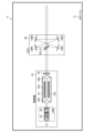
- FIG. 1 shows a schematic configuration of a laser device according to a comparative example.
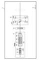
- FIG. 2 is an explanatory diagram of a method for measuring the transmittance of an optical pulse stretcher (OPS) of a laser device according to a comparative example.
- FIG. 3 is an explanatory diagram of a method for measuring the transmittance of the OPS of a laser device according to a comparative example.
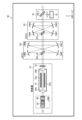
- FIG. 4 is a schematic diagram showing the configuration of a laser device according to the first embodiment.
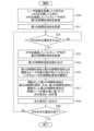
- FIG. 5 is a flowchart showing the procedure of the deterioration estimation method according to the first embodiment.
- FIG. 6 is a graph showing an example of a first temporal waveform and a second temporal waveform of a pulsed laser beam that has passed through an OPS.
- FIG. 7 is a schematic diagram showing a configuration of a laser device according to a modification of the first embodiment.
- FIG. 8 is a flowchart showing the procedure of the deterioration estimation method according to the second embodiment.
- FIG. 9 is a graph showing an example of a case where the second temporal waveform is normalized so that the maximum values of the first peaks of the first and second temporal waveforms are the same.
- FIG. 10 is a graph showing an example of a case where the second temporal waveform is normalized so that the maximum values of the second peaks of the first temporal waveform and the second temporal waveform are the same.
- FIG. 11 is a flowchart showing the procedure of a deterioration estimation method according to the third embodiment.
- FIG. 12 is a schematic diagram showing the configuration of a laser device according to the fourth embodiment.
- FIG. 13 is a flowchart showing the procedure of the deterioration estimation method according to the fourth embodiment.
- FIG. 14 is a graph showing an example of a first temporal waveform and a normalized second temporal waveform when the delay optical path length of the second OPS is twice that of the first OPS.
- FIG. 15 is a graph showing an example of a first temporal waveform and a normalized second temporal waveform when the delay optical path length of the second OPS is three times that of the first OPS.
- FIG. 16 is a schematic diagram showing the configuration of a laser device according to the fifth embodiment.
- FIG. 17 is a schematic diagram showing the configuration of a laser device according to the sixth embodiment.
- FIG. 18 shows a schematic configuration example of an exposure apparatus.
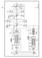
- FIG. 1 shows a schematic configuration of a laser device 4 according to the comparative example.
- the comparative example of the present disclosure is a form that the applicant recognizes as being known only by the applicant, and is not a publicly known example that the applicant acknowledges.
- the laser device 4 includes an oscillator 10 and an optical pulse stretcher (OPS) 50.
- OPS optical pulse stretcher
- the oscillator 10 includes a line narrowing module (LNM) 12, a chamber 14, and an output coupling mirror 18.
- the LNM 12 includes a prism beam expander 20 for narrowing the spectral width, and a grating 22.
- the grating 22 is Littrow-positioned so that the angle of incidence and the angle of diffraction are the same.
- the output coupling mirror 18 is a partially reflective mirror and is arranged to form an optical resonator together with the LNM 12.
- the reflectivity of the output coupling mirror 18 may be 20% to 30%.
- the chamber 14 is disposed on the optical path of the optical resonator and includes a pair of electrodes 25a, 25b and two windows 26a, 26b through which the laser light passes.
- An excimer laser gas is introduced into the chamber 14.
- the excimer laser gas may include, for example, Ar gas or Kr gas as a rare gas, F2 gas as a halogen gas, and Ne gas as a buffer gas.
- OPS50 includes a beam splitter BS_o1 and four concave mirrors CM1 to CM4 that form a delay optical path.
- the beam splitter BS_o1 and the concave mirrors CM1 to CM4 are positioned so that the laser light reflected by the beam splitter BS_o1 is reflected by the four concave mirrors CM1 to CM4, and the beam is imaged again by the beam splitter BS_o1.
- At least one of the concave mirrors CM1 to CM4 may be equipped with an actuator that changes the attitude angle.
- a pulsed high voltage is applied at a predetermined repetition frequency from a power supply (not shown) between the electrodes 25 a, 25 b in the chamber 14.
- a discharge occurs between the electrodes 25 a, 25 b, the laser gas is excited, and a pulsed laser beam narrowed in band by an optical resonator formed by the output coupling mirror 18 and the LNM 12 is output from the output coupling mirror 18.
- the pulsed laser light output from the output coupling mirror 18 enters the OPS 50, and a portion of the pulsed laser light passes through the delay optical path within the OPS 50 multiple times, thereby being expanded to a predetermined pulse width.
- FIGS 2 and 3 are explanatory diagrams of a method for measuring the transmittance of the OPS 50.
- an output meter 61 is installed so that the output of the pulsed laser light that has passed through the OPS 50 can be measured. Then, the output of the pulsed laser light that has passed through the OPS 50 is measured by the output meter 61.
- an output meter 62 is installed so that the output of the pulsed laser light before passing through the OPS 50 can be measured. Then, the output of the pulsed laser light before passing through the OPS 50 is measured by the output meter 62.
- the transmittance of the OPS 50 is calculated based on the output of the pulsed laser light before and after passing through the OPS 50. If the transmittance of the OPS 50 is below a preset value, it is assumed that the OPS 50 has deteriorated, and the OPS 50 is replaced. For example, if the transmittance of the OPS 50 is below 90%, it is assumed that the OPS 50 has deteriorated, and the OPS 50 is replaced.
- Embodiment 1 2.1 Configuration Fig. 4 shows a schematic configuration of a laser device 4A according to embodiment 1. Differences between the configuration of the laser device 4A shown in Fig. 4 and that shown in Fig. 1 will be described.
- the laser device 4A according to the first embodiment differs from the laser device 4 according to the comparative example in that a pulse waveform measuring device 70 is installed to measure the temporal waveform of the pulsed laser light that has passed through the OPS 50 in order to estimate deterioration of the OPS 50.
- the pulse waveform measuring device 70 may be installed permanently or may be installed only during maintenance.
- the pulse waveform measuring device 70 includes a beam splitter BS_t and a laser pulse detector 72. A portion of the pulse laser light incident on the pulse waveform measuring device 70 is reflected by the beam splitter BS_t and incident on the laser pulse detector 72. The pulse laser light transmitted through the beam splitter BS_t is output from the laser device 4A.
- the laser pulse detector 72 measures the temporal waveform of the pulse laser light with a time resolution of the nanosecond (ns) level.
- the laser pulse detector 72 may be, for example, a biplanar phototube.
- the temporal waveform of the pulse laser light is a pulse waveform that indicates the temporal change in the light intensity of the pulse laser light.
- the laser device 4A also includes a laser processor 80 that executes degradation estimation processing for the OPS 50 based on information obtained from the pulse waveform measuring device 70.
- the laser processor 80 is a processing device including a storage device in which a control program is stored, and a CPU (Central Processing Unit) that executes the control program.
- the laser processor 80 is specially configured or programmed to execute the various processes included in this disclosure.
- the laser processor 80 may include integrated circuits such as an FPGA (Field Programmable Gate Array) or an ASIC (Application Specific Integrated Circuit). Other configurations may be similar to those of the laser device 4 shown in FIG. 1.
- the laser processor 80 is an example of a "processor" in this disclosure.
- Fig. 5 is a flowchart showing the procedure of the deterioration estimation method according to the first embodiment.
- the laser processor 80 acquires a first temporal waveform of the pulsed laser light passing through the OPS 50, measured by the pulse waveform measuring instrument 70 when the laser device 4A is installed or the OPS 50 is replaced.
- the first temporal waveform is a temporal waveform measured in an initial state when the use of the OPS 50 is started.
- the timing at which the temporal waveform of the pulsed laser light is measured by the pulse waveform measuring instrument 70 when the laser device 4A is installed or the OPS 50 is replaced is an example of the "first measurement time" in the present disclosure.
- step S11 the laser processor 80 stores the first temporal waveform received from the pulse waveform measuring device 70 in a storage device.
- the laser processor 80 determines whether or not to perform a deterioration estimation of the OPS 50.
- a deterioration estimation of the OPS 50 There may be various conditions for performing the deterioration estimation. For example, it may be set so that the deterioration estimation is performed when the pulsed high voltage applied between the electrodes 25a, 25b in the chamber 14 when obtaining the target pulse energy increases by 10%, or when the gas pressure in the chamber 14 increases by 10%.
- the laser processor 80 may also receive an instruction to perform the deterioration estimation from a user interface as necessary, such as during regular maintenance, or may be configured to automatically perform the deterioration estimation periodically or irregularly according to a predetermined program.
- step S12 If the result of the determination in step S12 is No, the laser processor 80 loops through step S12.
- step S12 If the determination result in step S12 is Yes, the laser processor 80 proceeds to step S13.
- step S13 the laser processor 80 acquires a second temporal waveform of the pulsed laser light that has passed through the OPS 50, measured by the pulse waveform measuring device 70, when estimating deterioration of the OPS 50 during maintenance or the like.
- the timing at which the pulse waveform measuring device 70 measures the temporal waveform of the pulsed laser light when estimating deterioration during maintenance or the like is an example of the "second measurement time" in this disclosure.
- step S14 the laser processor 80 reads the first temporal waveform from the storage device. Then, in step S16, the laser processor 80 calculates a deterioration degree D_1 indicating the degree of deterioration of the OPS 50 based on the first temporal waveform and the second temporal waveform.
- the laser processor 80 calculates the deterioration degree D_1 in the following manner. That is, the laser processor 80 calculates the ratio R_12S between the maximum value P_1S of the first peak of the first temporal waveform and the maximum value P_2S of the second peak of the first temporal waveform using the following formula (1).
- the first peak refers to the peak that appears first among the multiple peaks included in the time waveform of the pulsed laser beam.
- the second peak refers to the peak that appears first among the multiple peaks included in the time waveform.
- the second peak is referred to as the kth peak.
- the third and subsequent peaks are referred to as the kth peak.
- the laser processor 80 calculates the ratio R_12E between the maximum value P_1E of the first peak of the second temporal waveform and the maximum value P_2E of the second peak using the following equation (2).
- step S18 the laser processor 80 outputs the calculation result of the deterioration degree D_1 to a display device (not shown) or the like of the laser device 4A.
- the laser processor 80 may estimate that the OPS 50 has deteriorated, and may output information such as a message or an alert to a display device, etc., to encourage replacement of the OPS 50.
- the first set value PV_1 is, for example, 10%.
- a user such as a field service engineer checks the calculation result of the deterioration degree D_1 shown on a display device or the like, and if the deterioration degree D_1 is equal to or greater than the first set value PV_1, replaces the OPS 50.
- the laser processor 80 may further calculate the number of pulses OPS1_dpls used by the OPS 50 at which the deterioration degree D_1 becomes the first set value PV_1.
- OPS1_dpls may be calculated by the following formula (4).
- OPS1_dpls PV_1/(D_1/OPS1_pls) (4)
- the value of OPS1_dpls calculated by formula (4) can be used to estimate (predict) a future replacement time for the OPS 50.
- the calculation result of OPS1_dpls may be output to a display device or the like together with the calculation result of the deterioration degree D_1.
- step S20 the laser processor 80 determines whether or not to end the process of estimating deterioration of the OPS 50. If the determination result in step S20 is No, the laser processor 80 returns to step S12.
- step S20 If the result of the determination in step S20 is Yes, the laser processor 80 ends the flowchart in FIG. 5.
- the pulse waveform measuring device 70 is installed in only one location, which shortens the measurement time.
- FIG. 7 shows a schematic configuration of a laser device 4B according to a modification of the first embodiment.
- the laser device 4B includes an oscillator 10A including a rear mirror 16, instead of the oscillator 10 including the LNM 12 shown in Fig. 5.
- the rear mirror 16 may be a total reflection mirror, and is arranged to configure an optical resonator together with the output coupling mirror 18.
- the other configurations are the same as those of the laser device 4A shown in Fig. 5.
- Embodiment 2 3.1 Configuration
- the configuration of the laser device according to the second embodiment may be similar to the configuration of the laser device 4A shown in FIG. 4 or the configuration of the laser device 4B shown in FIG.
- Fig. 8 is a flowchart showing the procedure of the deterioration estimation method according to embodiment 2. Differences between Fig. 8 and the flowchart in Fig. 5 will be described. The flowchart shown in Fig. 8 includes steps S15 and S17 instead of step S16 in Fig. 5.
- step S15 the laser processor 80 normalizes one of the first and second temporal waveforms so that the maximum value of one of the peaks (hereinafter referred to as the normalized peak) is the same when the first and second temporal waveforms are displayed so that their peak positions overlap.
- the normalized peak is set to the first peak
- the second temporal waveform is normalized based on the maximum value of the first peak of each of the first and second temporal waveforms.
- the normalized peak is set as the second peak
- the second temporal waveform is normalized based on the maximum value of the second peak of each of the first temporal waveform and the second temporal waveform.
- the first temporal waveform may be normalized in a manner not limited to the examples of FIG. 9 and FIG. 10.
- step S17 the laser processor 80 calculates a deterioration degree D_1 indicating the degree of deterioration of the OPS 50 from any one of the peaks other than the normalized peak.
- the peak used to calculate the deterioration degree D_1 is called the evaluation peak.
- the evaluation peak is the second peak, and in FIG. 10, the evaluation peak is the first peak.
- the deterioration degree D_1 is calculated by the following formula (5).
- step S17 the laser processor 80 proceeds to step S18.
- the other operations are the same as those in FIG.
- the normalized peak is the first peak and the evaluation peak is a peak after the third peak.
- the second peak is used as the evaluation peak. This is because from the third peak onwards, the maximum value of the peak becomes smaller and the effect of noise may become greater.
- the normalized peak may be the third peak or later.
- the deterioration degree D_1 can be calculated using formula (5).
- Embodiment 3 4.1 Configuration The configuration of the laser device according to the third embodiment may be similar to the configuration of the laser device 4A shown in FIG. 4 or the configuration of the laser device 4B shown in FIG.
- FIG. 11 is a flowchart showing the procedure of the deterioration estimation method according to embodiment 3. Differences between Fig. 11 and the flowchart in Fig. 8 will be described.
- the flowchart shown in Fig. 11 includes step S17B instead of step S17 in Fig. 8.
- the laser processor 80 calculates a deterioration degree D_1 indicating the degree of deterioration of the OPS 50 based on the respective areas of the standardized first temporal waveform and the second temporal waveform, or the respective areas of the first temporal waveform and the standardized second temporal waveform.
- the area is the value of the definite integral of the standardized first temporal waveform and the second temporal waveform, or the first temporal waveform and the standardized second temporal waveform.
- the laser processor 80 calculates the deterioration degree D_1 by the following formula (6).
- step S17B the laser processor 80 proceeds to step S18.
- the other operations are the same as those in FIG.
- Embodiment 4 12 is a schematic diagram showing the configuration of a laser device 4C according to embodiment 4.
- the laser device 4C will be described with respect to differences in configuration from the laser device 4A according to embodiment 1 shown in FIG.
- the laser device 4C of the fourth embodiment differs from the laser device 4A of the first embodiment in that an OPS 60 is disposed between the oscillator 10 and the OPS 50.
- OPS60 includes a beam splitter BS_o2 and four concave mirrors CM5 to CM8 that form a delay optical path.
- the beam splitter BS_o2 and the concave mirrors CM5 to CM8 are arranged so that the laser light reflected by the beam splitter BS_o2 is reflected by the four concave mirrors CM5 to CM8 and the beam is imaged again by the beam splitter BS_o2.
- At least one of the concave mirrors CM5 to CM8 may be equipped with an actuator that changes the attitude angle.
- the delay optical path length of OPS60 is longer than the delay optical path length of OPS50.
- the magnification of the delay optical path length of OPS60 to the delay optical path length of OPS50 is an integer of 2 or more, and this magnification is M.
- the other configurations are the same as those of the laser device 4A according to the first embodiment.
- OPS50 is an example of a "first optical pulse stretcher” in this disclosure
- OPS60 is an example of a “second optical pulse stretcher” in this disclosure
- the notation "OPS1” represents OPS50
- the notation "OPS2” represents OPS60
- the beam splitter BS_o1 of OPS50 is an example of a "first beam splitter” in this disclosure
- the delay optical path formed by the concave mirrors CM1 to CM4 is an example of a "first delay optical path” in this disclosure
- the concave mirrors CM1 to CM4 are an example of a “multiple mirrors forming the first delay optical path" in this disclosure.
- the beam splitter BS_o2 of OPS60 is an example of a "second beam splitter” in this disclosure
- the delay optical path formed by the concave mirrors CM5 to CM8 is an example of a "second delay optical path” in this disclosure
- Concave mirrors CM5 to CM8 are an example of the “multiple mirrors constituting the second delay optical path" in this disclosure.
- the operation of the device other than the OPS 60 is the same as that of the embodiment 1.
- the pulsed laser light output from the output coupling mirror 18 enters the OPS 60, and a part of the pulsed laser light passes through a delay optical path in the OPS 60 multiple times, whereby the pulsed laser light is expanded to a predetermined pulse width.
- the pulsed laser light that has passed through the OPS 60 enters the OPS 50.
- FIG. 13 is a flowchart showing the steps of the degradation estimation method according to the fourth embodiment.
- the laser processor 80 acquires a first temporal waveform of the pulsed laser light that has passed through the OPS 50, measured by the pulse waveform measuring device 70, when the laser device 4C is installed or when the OPS 50 or the OPS 60 is replaced.
- step S41 the laser processor 80 stores the first temporal waveform received from the pulse waveform measuring device 70 in a storage device.
- step S42 the laser processor 80 determines whether or not to perform degradation estimation for the entire OPS, including OPS 50 and OPS 60. If the determination result in step S42 is No, the laser processor 80 loops through step S42.
- step S42 If the determination result in step S42 is Yes, the laser processor 80 proceeds to step S43.
- step S43 the laser processor 80 acquires a second temporal waveform of the pulsed laser light that has passed through the OPS 50, measured by the pulse waveform measuring device 70, when estimating deterioration of the OPS 50 and OPS 60 during maintenance, etc.
- step S44 the laser processor 80 reads out the first temporal waveform from the storage device.
- the second peaks of the first and second temporal waveforms contain only the circulating light of the OPS 50, which has a short delay path length, and therefore the maximum value of the second peak decreases only due to the deterioration of the OPS 50, which has a short delay path length (see FIG. 14).
- the circulating light of the OPS 50 and the OPS 60 are included, and therefore from the third peak onwards, the maximum value of the peak decreases due to the deterioration of the OPS 50 and the OPS 60.
- step S45 the laser processor 80 selects a normalized peak from the first to Mth peaks, and normalizes one of the first and second temporal waveforms so that the maximum values of the normalized peaks of the first and second temporal waveforms are the same.
- FIG. 14 shows an example of a first temporal waveform and a standardized second temporal waveform when the delay path length of OPS 60 is twice that of OPS 50.
- the standardized peak is the first peak
- an example of a waveform after standardizing the second temporal waveform based on the maximum value of the first peaks of the first and second temporal waveforms is shown. Note that instead of standardizing the second temporal waveform, the first temporal waveform may be standardized.
- step S46 the laser processor 80 calculates a deterioration degree D_1 indicating the degree of deterioration of the OPS 50 based on the maximum value of the evaluation peaks of the normalized first temporal waveform and the second temporal waveform, or the maximum value of the evaluation peaks of the first temporal waveform and the normalized second temporal waveform. Note that it is preferable to select the evaluation peak from among the Mth peaks. In the case of FIG. 14, since the normalized peak is the first peak, the evaluation peak is the second peak.
- the deterioration degree D_1 is calculated using formula (5).
- step S47 the laser processor 80 calculates a degradation degree D_2 indicating the degree of degradation of the OPS 60 based on the maximum value of any two peaks up to the Mth peak and the M+1th peak.
- the degradation degree D_2 can be calculated from the maximum value of each of the first peak, the second peak, and the third peak.
- the maximum value of the first peak of the first temporal waveform or the normalized first temporal waveform is P_1S
- the maximum value of the second peak is P_2S
- the maximum value of the third peak is P_3S.
- the maximum value of the first peak of the second temporal waveform or the normalized second temporal waveform is P_1E
- the maximum value of the second peak is P_2E
- the transmittance of the beam splitter BS_o1 is denoted as T_BSo1.
- the transmittance is not limited to a value obtained by actual measurement, and may be a design value.
- the third peak of the temporal waveform measured by the pulse waveform measuring instrument 70 is a combination of the light that has passed through the beam splitter BS_o2 and traveled twice around the delay optical path of the OPS 50 and the light that has traveled once around the delay optical path of the OPS 60 and passed through the beam splitter BS_o1.
- the maximum value of the light that has passed through the beam splitter BS_o2 and made two trips around the delay optical path of OPS50 at the third peak of the first temporal waveform or the standardized first temporal waveform is P_3S1
- the maximum value of the light that has made one trip around the delay optical path of OPS60 and made through the beam splitter BS_o1 is P_3S2
- the maximum value of the light that has passed through the beam splitter BS_o2 and made two trips around the delay optical path of OPS50 at the third peak of the second temporal waveform or the standardized second temporal waveform is P_3E1
- the maximum value of the light that has made one trip around the delay optical path of OPS60 and made through the beam splitter BS_o1 is P_3E2.
- the third peak has the relationship of the following equations (7) and (8).
- P_3S P_3S1+P_3S2 (7)
- P_3E P_3E1+P_3E2 (8)
- the deterioration degree D_1 indicating the degree of deterioration of the OPS 50 is calculated by the formula (1).
- the laser processor 80 calculates P_3S1 using the following equation (9).
- P_3S1 P_2S ⁇ P_2S ⁇ T_BSo1 ⁇ T_BSo1/P_1S/(1-T_BSo1)/(1-T_BSo1) (9)
- the laser processor 80 calculates P_3SE1 using the following equation (10).
- step S48 the laser processor 80 outputs the calculation results of the deterioration degree D_1 and the deterioration degree D_2 to a display device (not shown) of the laser device 4. If the deterioration degree D_1 is equal to or greater than the first set value PV_1, For example, it is estimated that the OPS 50 has deteriorated, and the OPS 50 is replaced.
- the first set value PV_1 is, for example, 10%.
- the laser processor 80 may estimate that the OPS 60 has deteriorated, and may output information such as a message or an alert to a display device, etc., to encourage replacement of the OPS 60.
- the second set value PV_2 is, for example, 10%.
- a user such as a field service engineer checks the calculation result of the deterioration degree D_2 shown on a display device or the like, and if the deterioration degree D_2 is equal to or greater than the second set value PV_2, replaces the OPS 60.
- the laser processor 80 may calculate the number of pulses OPS1_dpls used by the OPS 50 at which the deterioration degree D_1 becomes the first set value PV_1 using equation (4). Furthermore, when the number of pulses used by the OPS 50 when measuring the second temporal waveform is OPS2_pls, the laser processor 80 may calculate the number of pulses OPS2_dpls used by the OPS 60 at which the deterioration degree D_2 becomes the second set value PV_2 using the following equation (12).
- OPS2_dpls PV_2/(D_2/OPS2_pls) (12)
- the value of OPS2_dpls calculated by formula (12) can be used to estimate (predict) the future replacement time of the OPS 60.
- the calculation results of OPS1_dpls and OPS2_dpls are output to a display device or the like together with the calculation results of the deterioration degrees D_1 and D_2. This is also fine.
- the delay path length of OPS 60 is twice that of OPS 50. However, even in cases other than twice, it is possible to grasp the peak positions where a decrease in the maximum peak value occurs due to deterioration of OPS 50 and OPS 60, and estimate the degree of deterioration of each OPS in a manner similar to that described above.
- FIG. 15 shows an example of a first temporal waveform and a normalized second temporal waveform when the delay path length of OPS 60 is three times that of OPS 50.
- the degree of deterioration D_2 is calculated from the maximum value of any two peaks up to the third peak and the maximum value of the fourth peak.
- Embodiment 5 shows a schematic configuration of a laser device 4D according to the fifth embodiment.
- the laser device 4D differs from the laser device 4A according to the first embodiment in that it includes an amplifier 90 between the oscillator 10 and the OPS 50, and a beam steering unit 120 is disposed between the oscillator 10 and the amplifier 90.
- the other configurations may be the same as those of the laser device 4A.
- the amplifier 90 includes a rear mirror 92, a chamber 94, and an output coupling mirror 98.
- the rear mirror 92 and the output coupling mirror 98 form a Fabry-Perot type optical resonator, and the chamber 94 is disposed on the optical path of this optical resonator.
- the rear mirror 92 is a partially reflective mirror with a reflectance of 50% to 90%.
- the output coupling mirror 98 is a partially reflective mirror with a reflectance of 10% to 30%.
- the chamber 94 includes a pair of electrodes 115a, 115b and two windows 116a, 116b through which the pulsed laser light passes.
- An excimer laser gas is introduced into the chamber 94.
- the excimer laser gas includes a rare gas, a halogen gas, and a buffer gas.
- the rare gas may be Ar gas or Kr gas.
- the halogen gas may be F2 gas.
- the buffer gas may be Ne gas.
- Beam steering unit 120 includes high-reflection mirror 121 and high-reflection mirror 122, and is positioned so that the pulsed laser light output from oscillator 10 enters amplifier 90.
- the amplifier 90 is not limited to a configuration having a Fabry-Perot type optical resonator, and may be a configuration having a ring resonator. Furthermore, instead of the amplifier 90, a single-pass amplifier or a multi-pass amplifier without an optical resonator may be used.
- the multi-pass amplifier may be, for example, a three-pass amplifier that amplifies the seed light by reflecting it off a cylindrical mirror and passing it through the discharge space three times.
- the pulsed laser light of an ultraviolet wavelength output from the oscillator 10 is incident on the rear mirror 92 of the amplifier 90 as seed light by the beam steering unit 120.
- a pulsed high voltage is applied between the electrodes 115a, 115b in the chamber 94 from a power supply (not shown) of the amplifier 90.
- a discharge occurs between the electrodes 115a, 115b, the laser gas is excited, and the seed light is amplified by a Fabry-Perot type optical resonator composed of the rear mirror 92 and the output coupling mirror 98, and the amplified pulsed laser light is output from the output coupling mirror 98.
- the pulsed laser light output from the output coupling mirror 98 is incident on the OPS 50.
- the operation of the OPS 50 and the operation for estimating deterioration of the OPS 50 are the same as in embodiment 1.
- Embodiment 6 7.1 Configuration Fig. 17 shows a schematic configuration of a laser device 4E according to the sixth embodiment.
- the laser device 4E differs from the laser device 4C according to the fourth embodiment in that it includes an amplifier 90 and a beam steering unit 120 is disposed between the oscillator 10 and the amplifier 90.
- the other configurations may be the same as those of the laser device 4C.
- the configuration of the amplifier 90 and the beam steering unit 120 is the same as that of embodiment 5 shown in FIG. 16.
- the oscillator 10 which is a gas laser
- the oscillation stage laser that outputs the seed light to be incident on the amplifier 90.
- a solid-state laser system including a semiconductor laser and a wavelength conversion system may be adopted.
- the wavelength conversion system may be configured using a nonlinear optical crystal. That is, the oscillation stage laser is not limited to a gas laser, and may be an ultraviolet solid-state laser that outputs pulsed laser light with an ultraviolet wavelength.
- the oscillation stage laser may be a solid-state laser that oscillates at a wavelength of about 193.4 nm, or an ultraviolet solid-state laser that outputs the fourth harmonic light of a titanium sapphire laser (wavelength of about 774 nm).
- FIG. 18 shows a schematic configuration example of an exposure apparatus 200.
- the exposure apparatus 200 includes an illumination optical system 206 and a projection optical system 208.
- the laser device 4A generates laser light and outputs the laser light to the exposure apparatus 200.
- the illumination optical system 206 illuminates a reticle pattern of a reticle (not shown) arranged on a reticle stage RT with the laser light incident from the laser device 4A.
- the projection optical system 208 reduces and projects the laser light transmitted through the reticle to form an image on a workpiece (not shown) arranged on a workpiece table WT.
- the workpiece is a photosensitive substrate such as a semiconductor wafer coated with photoresist.
- the exposure apparatus 200 exposes the workpiece to laser light reflecting the reticle pattern by synchronously translating the reticle stage RT and the workpiece table WT. After the reticle pattern is transferred to the semiconductor wafer by the exposure process described above, a semiconductor device can be manufactured through multiple processes.
- a semiconductor device is an example of an "electronic device" in this disclosure. It is not limited to the laser apparatus 4A, but laser apparatuses 4B to 4E, etc. may also be used.
Landscapes
- Physics & Mathematics (AREA)
- Electromagnetism (AREA)
- Engineering & Computer Science (AREA)
- Plasma & Fusion (AREA)
- Optics & Photonics (AREA)
- General Physics & Mathematics (AREA)
- Chemical & Material Sciences (AREA)
- Analytical Chemistry (AREA)
- Lasers (AREA)
Abstract
Description
1.比較例に係るレーザ装置の概要
1.1 構成
1.2 動作
1.3 比較例に係るOPSの劣化推定方法
1.4 課題
2.実施形態1
2.1 構成
2.2 動作
2.3 効果
2.4 変形例
2.4.1 構成
2.4.2 動作
2.4.3 効果
3.実施形態2
3.1 構成
3.2 動作
3.3 効果
4.実施形態3
4.1 構成
4.2 動作
4.3 効果
5.実施形態4
5.1 構成
5.2 動作
5.3 効果
5.4 変形例1
5.5 変形例2
6.実施形態5
6.1 構成
6.2 動作
6.3 効果
7.実施形態6
7.1 構成
7.2 動作
7.3 効果
8.レーザ装置の他の変形例
9.電子デバイスの製造方法について
10.その他
以下、本開示の実施形態について、図面を参照しながら詳しく説明する。以下に説明される実施形態は、本開示のいくつかの例を示すものであって、本開示の内容を限定するものではない。また、各実施形態で説明される構成及び動作の全てが本開示の構成及び動作として必須であるとは限らない。なお、同一の構成要素には同一の参照符号を付して、重複する説明を省略する。
1.1 構成
図1は、比較例に係るレーザ装置4の構成を概略的に示す。本開示の比較例とは、出願人のみによって知られていると出願人が認識している形態であって、出願人が自認している公知例ではない。レーザ装置4は、発振器10と、光学パルスストレッチャ(Optical Pulse Stretcher:OPS)50と、を含む。
不図示の制御部の制御に基づき、不図示の電源より所定の繰り返し周波数で、チャンバ14内の電極25a、25b間にパルス状の高電圧が印加される。電極25a、25b間で放電が発生すると、レーザガスが励起され、出力結合ミラー18とLNM12とで構成される光共振器によって狭帯域化されたパルスレーザ光が出力結合ミラー18から出力される。
OPS50が劣化すると、発振器負荷が上がり発振器10の寿命を短くするほか、パルスレーザ光の時間幅についての仕様を満たさなくなる。このため、定期メンテナンス時にOPS50の透過率を測定し、OPS50の劣化を推定している。
OPS50の透過率を測定してOPS50の劣化を推定する方法では、OPS50を通過する前後でレーザ光の出力を計測する必要がある。そのため、図2及び図3に示したように、出力計測器61、62を設置するための2箇所の設置場所が必要になる。
2.1 構成
図4は、実施形態1に係るレーザ装置4Aの構成を概略的に示す。図4に示すレーザ装置4Aについて、図1に示す構成と異なる点を説明する。
図5は、実施形態1に係る劣化推定方法の手順を示すフローチャートである。ステップS10において、レーザプロセッサ80は、レーザ装置4Aを設置したとき又はOPS50を交換したときにパルス波形計測器70で計測した、OPS50を通過したパルスレーザ光の第1の時間的波形を取得する。第1の時間的波形は、OPS50の使用を開始した初期の状態において計測した時間的波形である。レーザ装置4Aを設置したとき又はOPS50を交換したときにパルス波形計測器70によってパルスレーザ光の時間的波形を計測するタイミングは本開示における「第1の計測時」の一例である。
なお、第1のピークは、パルスレーザ光の時間的波形に含まれる複数のピークのうち1番目(最初)に現れるピークを指す。第2のピークは、時間的波形に含まれる複数のピークのうち2番目に現れるピークを指す。3番目以降についても同様に、k番目に現れるピークを第kのピークと呼ぶ。
そして、レーザプロセッサ80は、次式(3)により劣化度合D_1を計算する。
ステップS18において、レーザプロセッサ80は、劣化度合D_1の計算結果をレーザ装置4Aの不図示の表示装置等に出力する。
式(4)で計算されるOPS1_dplsの値から将来的なOPS50の交換時期を推定(予測)できる。劣化度合D_1の計算結果と共にOPS1_dplsの計算結果が表示装置等に出力されてもよい。
実施形態1に係る劣化推定方法によれば、次のような効果が得られる。
2.4.1 構成
図7は、実施形態1の変形例に係るレーザ装置4Bの構成を概略的に示す。レーザ装置4Bについて、図5に示す構成と異なる点を説明する。レーザ装置4Bは、図5に示すLNM12を含む発振器10の代わりに、リアミラー16を含む発振器10Aを備える。リアミラー16は、全反射ミラーであってよく、出力結合ミラー18と共に光共振器を構成するように配置される。その他の構成は、図5に示すレーザ装置4Aと同様である。
チャンバ14内の電極25a、25b間で放電が発生すると、レーザガスが励起され、出力結合ミラー18とリアミラー16とで構成される光共振器によって、波長が150nmから380nmの紫外線波長のパルスレーザ光が出力結合ミラー18から出力される。その他の動作は実施形態1に係るレーザ装置4Bの動作と同様である。
実施形態1の変形例に係るレーザ装置4Bの劣化推定方法の効果は、実施形態1の効果と同様である。
3.1 構成
実施形態2に係るレーザ装置の構成は、図4に示すレーザ装置4A又は図7に示すレーザ装置4Bの構成と同様であってよい。
図8は、実施形態2に係る劣化推定方法の手順を示すフローチャートである。図8について、図5のフローチャートと異なる点を説明する。図8に示すフローチャートは、図5のステップS16の代わりに、ステップS15及びステップS17を含む。
ステップS17の後、レーザプロセッサ80は、ステップS18に進む。その他の動作は、図5と同様である。
実施形態2の効果は、実施形態1の効果と同様である。
4.1 構成
実施形態3に係るレーザ装置の構成は、図4に示すレーザ装置4A又は図7に示すレーザ装置4Bの構成と同様であってよい。
図11は、実施形態3に係る劣化推定方法の手順を示すフローチャートである。図11について、図8のフローチャートと異なる点を説明する。図11に示すフローチャートは、図8のステップS17の代わりにステップS17Bを含む。
ステップS17Bの後、レーザプロセッサ80は、ステップS18に進む。その他の動作は、図5と同様である。
実施形態3の効果は、実施形態1の効果と同様である。
5.1 構成
図12は、実施形態4に係るレーザ装置4Cの構成を概略的に示す。レーザ装置4Cについて、図4に示す実施形態1に係るレーザ装置4Aの構成と異なる点を説明する。
OPS60以外の装置の動作は、実施形態1の動作と同様である。出力結合ミラー18から出力されたパルスレーザ光はOPS60に入射し、一部のパルスレーザ光がOPS60内の遅延光路を複数回通過することによって所定のパルス幅まで伸長される。OPS60を通過したパルスレーザ光は、OPS50に入射する。
P_3E=P_3E1+P_3E2 (8)
OPS50の劣化の度合を示す劣化度合D_1は式(1)により計算される。
レーザプロセッサ80は、P_3SE1を次式(10)で計算する。
そして、OPS60の劣化の度合を示す劣化度合D_2を次式(11)で計算する。
ステップS48において、レーザプロセッサ80は、劣化度合D_1と劣化度合D_2との計算結果をレーザ装置4の不図示の表示装置等に出力する。そして、劣化度合D_1が第1の設定値PV_1以上であれば、OPS50が劣化したと推定し、OPS50を交換する。第1の設定値PV_1は例えば、10%である。
式(12)で計算されるOPS2_dplsの値から将来的なOPS60の交換時期を推定(予測)できる。劣化度合D_1及び劣化度合D_2の計算結果と共にOPS1_dpls及びOPS2_dplsの計算結果が表示装置等に出力されてもよい。
実施形態4の効果は実施形態1の効果と同様である。図12のように光学パルスストレッチャ50、60を2つ配置した場合でも、それぞれのOPSの劣化の度合を推定することができる。
実施形態4では、OPS60の遅延光路長はOPS50の遅延光路長の2倍の場合を示したが、2倍以外の場合でも、OPS50とOPS60との劣化によるピークの最大値減少が生ずるピーク位置を把握し、上記と同様の方法でそれぞれのOPSの劣化の度合を推定することができる。
また、実施形態4では、発振器10とOPS50との間にOPS60を配置した場合の劣化度合D_1及び劣化度合D_2の計算方法を示したが、OPS50とOPS60との配置関係は入れ替え可能である。すなわち、発振器10とOPS60との間にOPS50を配置した構成の場合も、式(5)でOPS50の劣化度合D_1を計算することができ、式(11)でOPS60の劣化度合D_2を計算することができる。
6.1 構成
図16は、実施形態5に係るレーザ装置4Dの構成を概略的に示す。レーザ装置4Dの構成について、図4に示す実施形態1に係るレーザ装置4Aの構成と異なる点を説明する。レーザ装置4Dは、発振器10とOPS50との間に増幅器90を含み、発振器10と増幅器90との間にビームステアリングユニット120が配置されている点で実施形態1に係るレーザ装置4Aと異なる。その他の構成は、レーザ装置4Aと同様であってよい。
発振器10から出力された紫外線波長のパルスレーザ光は、ビームステアリングユニット120によって、増幅器90のリアミラー92にシード光として入射する。
実施形態5の効果は実施形態1の効果と同様である。
7.1 構成
図17は、実施形態6に係るレーザ装置4Eの構成を概略的に示す。レーザ装置4Eの構成について、図12に示す実施形態4に係るレーザ装置4Cの構成と異なる点を説明する。レーザ装置4Eは、増幅器90を含み、発振器10と増幅器90との間にビームステアリングユニット120が配置されている点で実施形態4に係るレーザ装置4Cと異なる。その他の構成は、レーザ装置4Cと同様であってよい。
レーザ装置4Eにおける発振器10、ビームステアリングユニット120及び増幅器90の動作は、実施形態5の動作と同様である。増幅器90の出力結合ミラー98から出力されたパルスレーザ光は、OPS60に入射する。OPS60及びOPS50の動作、並びに、OPS60及びOPS50の劣化推定についての動作は実施形態4の動作と同様である。
実施形態6の効果は実施形態4の効果と同様である。
図16及び図17では、増幅器90に入射させるシード光を出力する発振段レーザとして、ガスレーザである発振器10を用いる例を説明したが、発振器10の代わりに、例えば、半導体レーザと、波長変換システムとを含む固体レーザシステムを採用してもよい。波長変換システムは非線形光学結晶を用いて構成し得る。すなわち、発振段レーザは、ガスレーザに限らず、紫外線波長のパルスレーザ光を出力する紫外線固体レーザであってもよい。例えば、発振段レーザは、波長約193.4nmを発振する固体レーザ、あるいは、チタンサファイヤレーザ(波長約774nm)の第4高調波光を出力する紫外線固体レーザなどでもよい。
図18は、露光装置200の構成例を概略的に示す。露光装置200は、照明光学系206と投影光学系208とを含む。レーザ装置4Aはレーザ光を生成し、レーザ光を露光装置200に出力する。照明光学系206は、レーザ装置4Aから入射したレーザ光によって、レチクルステージRT上に配置された不図示のレチクルのレチクルパターンを照明する。投影光学系208は、レチクルを透過したレーザ光を、縮小投影してワークピーステーブルWT上に配置された不図示のワークピースに結像させる。ワークピースはフォトレジストが塗布された半導体ウエハ等の感光基板である。
上記の説明は、制限ではなく単なる例示を意図している。したがって、特許請求の範囲を逸脱することなく本開示の実施形態に変更を加えることができることは、当業者には明らかである。また、本開示の実施形態を組み合わせて使用することも当業者には明らかである。
Claims (20)
- パルスレーザ光のパルス幅を伸長する光学パルスストレッチャの劣化推定方法であって、
前記光学パルスストレッチャによりパルス幅が伸長された前記パルスレーザ光の第1の計測時の第1の時間的波形を取得し、
前記第1の計測時より後の第2の計測時の、前記光学パルスストレッチャによりパルス幅が伸長された前記パルスレーザ光の第2の時間的波形を取得し、
前記第1の時間的波形と前記第2の時間的波形とに基づいて、前記光学パルスストレッチャの劣化の度合を推定する、
劣化推定方法。 - 請求項1に記載の劣化推定方法であって、
前記第1の時間的波形における第1のピークの最大値P_1Sと第2のピークの最大値P_2Sとの比R_12Sを次式(a)で計算し、
R_12S=P_2S/P_1S (a)
前記第2の時間的波形における第1のピークの最大値P_1Eと第2のピークの最大値P_2Eとの比R_12Eを次式(b)で計算し、
R_12E=P_2E/P_1E (b)
前記光学パルスストレッチャの劣化の度合を示す劣化度合D_1を次式(c)で計算する、
D_1=R_12S-R_12E (c)
劣化推定方法。 - 請求項1に記載の劣化推定方法であって、
前記第1の時間的波形と前記第2の時間的波形とのそれぞれに含まれる複数のピークのうちから定められた規格化ピークの最大値が同じになるように、いずれか一方の時間的波形を規格化し、
前記規格化した前記第1の時間的波形と前記第2の時間的波形とに基づいて、又は、前記第1の時間的波形と前記規格化した前記第2の時間的波形とに基づいて、前記光学パルスストレッチャの劣化の度合を示す劣化度合を計算する、
劣化推定方法。 - 請求項3に記載の劣化推定方法であって、
前記規格化ピーク以外のいずれか1つのピークを評価ピークとし、前記第1の時間的波形又は前記規格化した前記第1の時間的波形の前記評価ピークの最大値をP_AS1とし、前記第2の時間的波形又は前記規格化した前記第2の時間的波形の前記評価ピークの最大値をP_AE1としたとき、前記光学パルスストレッチャの劣化の度合を示す劣化度合D_1を次式(d)で計算する、
D_1=|1-P_AE1/P_AS1| (d)
劣化推定方法。 - 請求項3に記載の劣化推定方法であって、
前記第1の時間的波形又は前記規格化した前記第1の時間的波形の面積をS_2Sとし、前記第2の時間的波形又は前記規格化した前記第2の時間的波形の面積をS_2Eとしたとき、
前記光学パルスストレッチャの劣化の度合を示す劣化度合D_1を次式(e)で計算する、
D_1=1-S_2E/S_2S (e)
劣化推定方法。 - 請求項1に記載の劣化推定方法であって、
前記第1の時間的波形と前記第2の時間的波形とを基に推定された前記光学パルスストレッチャの劣化の度合を示す劣化度合D_1を表示装置に出力する、
劣化推定方法。 - 請求項1に記載の劣化推定方法であって、
前記第1の時間的波形と前記第2の時間的波形とを基に推定された前記光学パルスストレッチャの劣化の度合を示す劣化度合D_1が第1の設定値以上である場合に前記光学パルスストレッチャが劣化したと推定する、
劣化推定方法。 - 請求項1に記載の劣化推定方法であって、
前記第2の計測時の前記光学パルスストレッチャの使用パルス数をOPS1_plsとし、第1の設定値をPV_1としたとき、
前記光学パルスストレッチャの劣化の度合を示す劣化度合D_1が前記第1の設定値PV_1になる前記光学パルスストレッチャの使用パルス数OPS1_dplsを次式(f)で計算する、
OPS1_dpls=PV_1/(D_1/OPS1_pls) (f)
劣化推定方法。 - 請求項1に記載の劣化推定方法であって、
前記光学パルスストレッチャである第1の光学パルスストレッチャは、
第1のビームスプリッタと、第1の遅延光路を構成する複数のミラーと、を含み、
前記第1の光学パルスストレッチャを備えるレーザ装置は、さらに、第2のビームスプリッタと、第2の遅延光路を構成する複数のミラーと、を含む第2の光学パルスストレッチャを備え、
前記第2の光学パルスストレッチャの遅延光路長は、前記第1の光学パルスストレッチャの遅延光路長のM倍であり、Mは2以上の整数であるとき、
前記第1の時間的波形及び第2の時間的波形のそれぞれにおける1番目からM番目までのピークのいずれか1つのピークを規格化ピークとし、前記第1の時間的波形と前記第2の時間的波形との前記規格化ピークの最大値に基づいて、いずれか一方の時間的波形を規格化し、
前記規格化ピーク以外の前記M番目までのピークのいずれか1つのピークを評価ピークとし、前記第1の時間的波形又は前記規格化した前記第1の時間的波形の前記評価ピークの最大値と、前記第2の時間的波形又は前記規格化した前記第2の時間的波形の前記評価ピークの最大値とを基に、前記第1の光学パルスストレッチャの劣化の度合を示す劣化度合D_1を計算し、
前記第1の時間的波形又は前記規格化した前記第1の時間的波形と、前記第2の時間的波形又は前記規格化した前記第2の時間的波形との前記M番目までのピークのいずれか2つのピークと、M+1番目のピークとのそれぞれのピークの最大値を基に、前記第2の光学パルスストレッチャの劣化の度合を示す劣化度合D_2を計算する、
劣化推定方法。 - 請求項9に記載の劣化推定方法であって、
前記第2の光学パルスストレッチャの遅延光路長は前記第1の光学パルスストレッチャの遅延光路長の2倍であり、
前記第1の時間的波形又は前記規格化した前記第1の時間的波形の第1のピークの最大値をP_1S、第2のピークの最大値をP_2S、第3のピークの最大値をP_3Sとし、
前記第2の時間的波形又は前記規格化した前記第2の時間的波形の第2のピークの最大値をP_2E、第3のピークの最大値をP_3Eとし、
前記第1の時間的波形又は前記規格化した前記第1の時間的波形の第3のピークにおいて前記第2のビームスプリッタを透過し前記第1の光学パルスストレッチャの前記第1の遅延光路を2周した光の最大値をP_3S1、前記第2の時間的波形又は前記規格化した前記第2の時間的波形の第3のピークにおいて前記第2のビームスプリッタを透過し前記第1の光学パルスストレッチャの前記第1の遅延光路を2周した光の最大値をP_3E1とし、又は、前記第1の時間的波形又は前記規格化した前記第1の時間的波形の第3のピークにおいて前記第1の光学パルスストレッチャの前記第1の遅延光路を2周して前記第2のビームスプリッタを透過した光の最大値をP_3S1、前記第2の時間的波形又は前記規格化した前記第2の時間的波形の第3のピークにおいて前記第1の光学パルスストレッチャの前記第1の遅延光路を2周して前記第2のビームスプリッタを透過した光の最大値をP_3E1とし、
前記第1のビームスプリッタの透過率をT_BSo1とし、
前記規格化ピークを第1のピークとし、前記評価ピークを第2のピークとしたとき、
前記劣化度合D_1を次式(g)で計算し、
D_1=|1-P_2E/P_2S| (g)
P_3S1を次式(h)で計算し、
P_3S1=P_2S×P_2S×T_BSo1×T_BSo1/P_1S/(1-T_BSo1)/(1-T_BSo1) (h)
P_3E1を次式(i)で計算し、
P_3E1=(1-D_1)×(1-D_1)×P_3S1 (i)
前記劣化度合D_2を次式(j)で計算する、
D_2=1-(P_3E-P_3E1)/(P_3S-P_3S1) (j)
劣化推定方法。 - パルスレーザ光を出力する発振器と、
前記パルスレーザ光のパルス幅を伸長する光学パルスストレッチャと、
第1の計測時に前記光学パルスストレッチャによりパルス幅が伸長された前記パルスレーザ光の第1の時間的波形を計測し、前記第1の計測時より後の第2の計測時に前記光学パルスストレッチャによりパルス幅が伸長された前記パルスレーザ光の第2の時間的波形を計測するパルス波形計測器と、
前記第1の時間的波形と前記第2の時間的波形とに基づいて、前記光学パルスストレッチャの劣化の度合を推定するプロセッサと、
を備えるレーザ装置。 - 請求項11に記載のレーザ装置であって、
前記プロセッサは、
前記第1の時間的波形における第1のピークの最大値P_1Sと第2のピークの最大値P_2Sとの比R_12Sを次式(a)で計算し、
R_12S=P_2S/P_1S (a)
前記第2の時間的波形における第1のピークの最大値P_1Eと第2のピークの最大値P_2Eとの比R_12Eを次式(b)で計算し、
R_12E=P_2E/P_1E (b)
前記光学パルスストレッチャの劣化の度合を示す劣化度合D_1を次式(c)で計算する、
D_1=R_12S-R_12E (c)
レーザ装置。 - 請求項11に記載のレーザ装置であって、
前記プロセッサは、
前記第1の時間的波形と前記第2の時間的波形とのそれぞれに含まれる複数のピークのうちから定められた規格化ピークの最大値が同じになるように、いずれか一方の時間的波形を規格化し、
前記規格化した前記第1の時間的波形と前記第2の時間的波形とに基づいて、又は、前記第1の時間的波形と前記規格化した前記第2の時間的波形とに基づいて、前記光学パルスストレッチャの劣化の度合を示す劣化度合を計算する、
レーザ装置。 - 請求項13に記載のレーザ装置であって、
前記プロセッサは、
前記規格化ピーク以外のいずれか1つのピークを評価ピークとし、前記第1の時間的波形又は前記規格化した前記第1の時間的波形の前記評価ピークの最大値をP_AS1とし、前記第2の時間的波形又は前記規格化した前記第2の時間的波形の前記評価ピークの最大値をP_AE1としたとき、前記光学パルスストレッチャの劣化の度合を示す劣化度合D_1を次式(d)で計算する、
D_1=|1-P_AE1/P_AS1| (d)
レーザ装置。 - 請求項13に記載のレーザ装置であって、
前記プロセッサは、
前記第1の時間的波形又は前記規格化した前記第1の時間的波形の面積をS_2Sとし、前記第2の時間的波形又は前記規格化した前記第2の時間的波形の面積をS_2Eとしたとき、
前記光学パルスストレッチャの劣化の度合を示す劣化度合D_1を次式(e)で計算する、
D_1=1-S_2E/S_2S (e)
レーザ装置。 - 請求項11に記載のレーザ装置であって、
前記プロセッサは、
前記第2の計測時の前記光学パルスストレッチャの使用パルス数をOPS1_plsとし、第1の設定値をPV_1としたとき、
前記光学パルスストレッチャの劣化の度合を示す劣化度合D_1が前記第1の設定値PV_1になる前記光学パルスストレッチャの使用パルス数OPS1_dplsを次式(f)で計算する、
OPS1_dpls=PV_1/(D_1/OPS1_pls) (f)
レーザ装置。 - 請求項11に記載のレーザ装置であって、さらに、
前記発振器と前記光学パルスストレッチャとの間に増幅器を備える、
レーザ装置。 - 請求項11に記載のレーザ装置であって、
前記光学パルスストレッチャである第1の光学パルスストレッチャの他に、第2の光学パルスストレッチャをさらに備え、
前記第1の光学パルスストレッチャは、第1のビームスプリッタと、第1の遅延光路を構成する複数のミラーと、を含み、
前記第2の光学パルスストレッチャは、第2のビームスプリッタと、第2の遅延光路を構成する複数のミラーと、を含み、
前記第2の光学パルスストレッチャの遅延光路長は、前記第1の光学パルスストレッチャの遅延光路長のM倍であって、Mは2以上の整数であり、
前記プロセッサは、
前記第1の時間的波形及び第2の時間的波形のそれぞれにおけるM番目までのピークのいずれか1つのピークを規格化ピークとし、前記第1の時間的波形と前記第2の時間的波形との前記規格化ピークの最大値に基づいていずれか一方の時間的波形を規格化し、
前記規格化ピーク以外の前記M番目までのピークのいずれか1つのピークを評価ピークとし、前記第1の時間的波形又は規格化した前記第1の時間的波形の前記評価ピークの最大値と、前記第2の時間的波形又は規格化した前記第2の時間的波形の前記評価ピークの最大値とにより前記第1の光学パルスストレッチャの劣化の度合を示す劣化度合D_1を計算し、
前記第1の時間的波形又は規格化した前記第1の時間的波形と、前記第2の時間的波形又は規格化した前記第2の時間的波形との前記M番目までのピークのいずれか2つのピークと、M+1番目のピークとのそれぞれのピークの最大値により、前記第2の光学パルスストレッチャの劣化の度合を示す劣化度合D_2を計算する、
レーザ装置。 - 請求項18に記載のレーザ装置であって、
前記第2の光学パルスストレッチャの遅延光路長は前記第1の光学パルスストレッチャの遅延光路長の2倍であり、
前記第1の時間的波形又は前記規格化した前記第1の時間的波形の第1のピークの最大値をP_1S、第2のピークの最大値をP_2S、第3のピークの最大値をP_3Sとし、
前記第2の時間的波形又は前記規格化した前記第2の時間的波形の第2のピークの最大値をP_2E、第3のピークの最大値をP_3Eとし、
前記第1の時間的波形又は前記規格化した前記第1の時間的波形の第3のピークにおいて前記第2のビームスプリッタを透過し前記第1の光学パルスストレッチャの前記第1の遅延光路を2周した光の最大値をP_3S1、前記第2の時間的波形又は前記規格化した前記第2の時間的波形の第3のピークにおいて前記第2のビームスプリッタを透過し前記第1の光学パルスストレッチャの前記第1の遅延光路を2周した光の最大値をP_3E1とし、又は、前記第1の時間的波形又は前記規格化した前記第1の時間的波形の第3のピークにおいて前記第1の光学パルスストレッチャの前記第1の遅延光路を2周して前記第2のビームスプリッタを透過した光の最大値をP_3S1、前記第2の時間的波形又は前記規格化した前記第2の時間的波形の第3のピークにおいて前記第1の光学パルスストレッチャの前記第1の遅延光路を2周して前記第2のビームスプリッタを透過した光の最大値をP_3E1とし、
前記第1のビームスプリッタの透過率をT_BSo1とし、
前記規格化ピークを第1のピークとし、前記評価ピークを第2のピークとしたとき、
前記劣化度合D_1を次式(g)で計算し、
D_1=|1-P_2E/P_2S| (g)
P_3S1を次式(h)で計算し、
P_3S1=P_2S×P_2S×T_BSo1×T_BSo1/P_1S/(1-T_BSo1)/(1-T_BSo1) (h)
P_3E1を次式(i)で計算し、
P_3E1=(1-D_1)×(1-D_1)×P_3S1 (i)
前記劣化度合D_2を次式(j)で計算する、
D_2=1-(P_3E-P_3E1)/(P_3S-P_3S1) (j)
レーザ装置。 - 電子デバイスの製造方法であって、
パルスレーザ光を出力する発振器と、
前記パルスレーザ光のパルス幅を伸長する光学パルスストレッチャと、
第1の計測時に前記光学パルスストレッチャによりパルス幅が伸長された前記パルスレーザ光の第1の時間的波形を計測し、前記第1の計測時より後の第2の計測時に前記光学パルスストレッチャによりパルス幅が伸長された前記パルスレーザ光の第2の時間的波形を計測するパルス波形計測器と、
前記第1の時間的波形と前記第2の時間的波形とに基づいて、前記光学パルスストレッチャの劣化の度合を推定するプロセッサと、を備えるレーザ装置によって前記パルス幅が伸長されたレーザ光を生成し、
前記レーザ光を露光装置に出力し、
電子デバイスを製造するために、前記露光装置内で感光基板に前記レーザ光を露光することを含む電子デバイスの製造方法。
Priority Applications (4)
| Application Number | Priority Date | Filing Date | Title |
|---|---|---|---|
| CN202380090333.5A CN120457605A (zh) | 2023-02-06 | 2023-02-06 | 劣化估计方法、激光装置和电子器件的制造方法 |
| PCT/JP2023/003836 WO2024166185A1 (ja) | 2023-02-06 | 2023-02-06 | 劣化推定方法、レーザ装置及び電子デバイスの製造方法 |
| JP2024575892A JPWO2024166185A1 (ja) | 2023-02-06 | 2023-02-06 | |
| US19/264,346 US20250341444A1 (en) | 2023-02-06 | 2025-07-09 | Deterioration estimation method, laser device, and electronic device manufacturing method |
Applications Claiming Priority (1)
| Application Number | Priority Date | Filing Date | Title |
|---|---|---|---|
| PCT/JP2023/003836 WO2024166185A1 (ja) | 2023-02-06 | 2023-02-06 | 劣化推定方法、レーザ装置及び電子デバイスの製造方法 |
Related Child Applications (1)
| Application Number | Title | Priority Date | Filing Date |
|---|---|---|---|
| US19/264,346 Continuation US20250341444A1 (en) | 2023-02-06 | 2025-07-09 | Deterioration estimation method, laser device, and electronic device manufacturing method |
Publications (1)
| Publication Number | Publication Date |
|---|---|
| WO2024166185A1 true WO2024166185A1 (ja) | 2024-08-15 |
Family
ID=92262122
Family Applications (1)
| Application Number | Title | Priority Date | Filing Date |
|---|---|---|---|
| PCT/JP2023/003836 Ceased WO2024166185A1 (ja) | 2023-02-06 | 2023-02-06 | 劣化推定方法、レーザ装置及び電子デバイスの製造方法 |
Country Status (4)
| Country | Link |
|---|---|
| US (1) | US20250341444A1 (ja) |
| JP (1) | JPWO2024166185A1 (ja) |
| CN (1) | CN120457605A (ja) |
| WO (1) | WO2024166185A1 (ja) |
Citations (6)
| Publication number | Priority date | Publication date | Assignee | Title |
|---|---|---|---|---|
| JP2003214949A (ja) * | 2002-01-25 | 2003-07-30 | Gigaphoton Inc | モニタ装置及び紫外線レーザ装置 |
| JP2011515650A (ja) * | 2007-12-20 | 2011-05-19 | サイマー インコーポレイテッド | Euv光源構成要素及びその製造、使用及び修復方法 |
| US20110235663A1 (en) * | 2010-03-24 | 2011-09-29 | Akins Robert P | Method and System for Managing Light Source Operation |
| WO2014038584A1 (ja) * | 2012-09-07 | 2014-03-13 | ギガフォトン株式会社 | レーザ装置及びレーザ装置の制御方法 |
| JP2019523434A (ja) * | 2016-07-12 | 2019-08-22 | サイマー リミテッド ライアビリティ カンパニー | リソグラフィ光学部品の調節及びモニタリング |
| WO2020161865A1 (ja) * | 2019-02-07 | 2020-08-13 | ギガフォトン株式会社 | 機械学習方法、消耗品管理装置、及びコンピュータ可読媒体 |
-
2023
- 2023-02-06 WO PCT/JP2023/003836 patent/WO2024166185A1/ja not_active Ceased
- 2023-02-06 JP JP2024575892A patent/JPWO2024166185A1/ja active Pending
- 2023-02-06 CN CN202380090333.5A patent/CN120457605A/zh active Pending
-
2025
- 2025-07-09 US US19/264,346 patent/US20250341444A1/en active Pending
Patent Citations (6)
| Publication number | Priority date | Publication date | Assignee | Title |
|---|---|---|---|---|
| JP2003214949A (ja) * | 2002-01-25 | 2003-07-30 | Gigaphoton Inc | モニタ装置及び紫外線レーザ装置 |
| JP2011515650A (ja) * | 2007-12-20 | 2011-05-19 | サイマー インコーポレイテッド | Euv光源構成要素及びその製造、使用及び修復方法 |
| US20110235663A1 (en) * | 2010-03-24 | 2011-09-29 | Akins Robert P | Method and System for Managing Light Source Operation |
| WO2014038584A1 (ja) * | 2012-09-07 | 2014-03-13 | ギガフォトン株式会社 | レーザ装置及びレーザ装置の制御方法 |
| JP2019523434A (ja) * | 2016-07-12 | 2019-08-22 | サイマー リミテッド ライアビリティ カンパニー | リソグラフィ光学部品の調節及びモニタリング |
| WO2020161865A1 (ja) * | 2019-02-07 | 2020-08-13 | ギガフォトン株式会社 | 機械学習方法、消耗品管理装置、及びコンピュータ可読媒体 |
Also Published As
| Publication number | Publication date |
|---|---|
| US20250341444A1 (en) | 2025-11-06 |
| CN120457605A (zh) | 2025-08-08 |
| JPWO2024166185A1 (ja) | 2024-08-15 |
Similar Documents
| Publication | Publication Date | Title |
|---|---|---|
| CN112771737B (zh) | 激光系统和电子器件的制造方法 | |
| JP5104305B2 (ja) | 露光装置、露光方法及びデバイス製造方法 | |
| US9882343B2 (en) | Narrow band laser apparatus | |
| CN115039032B (zh) | 曝光系统、激光控制参数的生成方法和电子器件的制造方法 | |
| CN109314365B (zh) | 激光系统 | |
| CN112640230B (zh) | 激光系统和电子器件的制造方法 | |
| US20210294223A1 (en) | Wavelength control method of laser apparatus and electronic device manufacturing method | |
| JP7461454B2 (ja) | 露光システム及び電子デバイスの製造方法 | |
| JPH07170009A (ja) | 光源装置 | |
| CN113383469B (zh) | 激光装置和电子器件的制造方法 | |
| JP7480275B2 (ja) | 露光システム、レーザ制御パラメータの作成方法、及び電子デバイスの製造方法 | |
| US12573817B2 (en) | Exposure system, exposure method, and electronic device manufacturing method | |
| JP2026053448A (ja) | スペクトル波形の制御方法、レーザ装置、露光装置、及び電子デバイスの製造方法 | |
| WO2024166185A1 (ja) | 劣化推定方法、レーザ装置及び電子デバイスの製造方法 | |
| CN115997171B (zh) | 电子器件的制造方法 | |
| CN115038944B (zh) | 传感器劣化判定方法 | |
| CN115039298B (zh) | 激光装置和电子器件的制造方法 | |
| JP5141359B2 (ja) | スペクトル幅計測器の校正方法、スペクトル幅計測器の校正装置、狭帯域化レーザ装置、露光装置及び電子デバイスの製造方法 | |
| JP2007142052A (ja) | 露光装置、レーザ光源、露光方法、及びデバイス製造方法 | |
| JP7648994B2 (ja) | レーザ装置、レーザ発振方法及び電子デバイスの製造方法 | |
| JP7782814B2 (ja) | 光学パルスストレッチャ、レーザ装置及び電子デバイスの製造方法 | |
| US20250364775A1 (en) | Laser device, exposure apparatus, and electronic device manufacturing method | |
| US20250210924A1 (en) | Laser apparatus and electronic device manufacturing method | |
| US20240405502A1 (en) | Laser apparatus, method for measuring spectral linewidth, and method for manufacturing electronic devices | |
| JP2025101951A (ja) | レーザ装置、及び電子デバイスの製造方法 |
Legal Events
| Date | Code | Title | Description |
|---|---|---|---|
| 121 | Ep: the epo has been informed by wipo that ep was designated in this application |
Ref document number: 23921021 Country of ref document: EP Kind code of ref document: A1 |
|
| ENP | Entry into the national phase |
Ref document number: 2024575892 Country of ref document: JP Kind code of ref document: A |
|
| WWE | Wipo information: entry into national phase |
Ref document number: 2024575892 Country of ref document: JP |
|
| WWE | Wipo information: entry into national phase |
Ref document number: 202380090333.5 Country of ref document: CN |
|
| WWP | Wipo information: published in national office |
Ref document number: 202380090333.5 Country of ref document: CN |
|
| NENP | Non-entry into the national phase |
Ref country code: DE |
|
| 122 | Ep: pct application non-entry in european phase |
Ref document number: 23921021 Country of ref document: EP Kind code of ref document: A1 |