WO2024165961A1 - 半導体装置、及びその作製方法 - Google Patents
半導体装置、及びその作製方法 Download PDFInfo
- Publication number
- WO2024165961A1 WO2024165961A1 PCT/IB2024/051011 IB2024051011W WO2024165961A1 WO 2024165961 A1 WO2024165961 A1 WO 2024165961A1 IB 2024051011 W IB2024051011 W IB 2024051011W WO 2024165961 A1 WO2024165961 A1 WO 2024165961A1
- Authority
- WO
- WIPO (PCT)
- Prior art keywords
- layer
- conductive layer
- opening
- insulating layer
- semiconductor
- Prior art date
- Legal status (The legal status is an assumption and is not a legal conclusion. Google has not performed a legal analysis and makes no representation as to the accuracy of the status listed.)
- Ceased
Links
Images


















































Classifications
-
- G—PHYSICS
- G02—OPTICS
- G02F—OPTICAL DEVICES OR ARRANGEMENTS FOR THE CONTROL OF LIGHT BY MODIFICATION OF THE OPTICAL PROPERTIES OF THE MEDIA OF THE ELEMENTS INVOLVED THEREIN; NON-LINEAR OPTICS; FREQUENCY-CHANGING OF LIGHT; OPTICAL LOGIC ELEMENTS; OPTICAL ANALOGUE/DIGITAL CONVERTERS
- G02F1/00—Devices or arrangements for the control of the intensity, colour, phase, polarisation or direction of light arriving from an independent light source, e.g. switching, gating or modulating; Non-linear optics
- G02F1/01—Devices or arrangements for the control of the intensity, colour, phase, polarisation or direction of light arriving from an independent light source, e.g. switching, gating or modulating; Non-linear optics for the control of the intensity, phase, polarisation or colour
- G02F1/13—Devices or arrangements for the control of the intensity, colour, phase, polarisation or direction of light arriving from an independent light source, e.g. switching, gating or modulating; Non-linear optics for the control of the intensity, phase, polarisation or colour based on liquid crystals, e.g. single liquid crystal display cells
- G02F1/133—Constructional arrangements; Operation of liquid crystal cells; Circuit arrangements
- G02F1/136—Liquid crystal cells structurally associated with a semi-conducting layer or substrate, e.g. cells forming part of an integrated circuit
- G02F1/1362—Active matrix addressed cells
- G02F1/1368—Active matrix addressed cells in which the switching element is a three-electrode device
-
- G—PHYSICS
- G09—EDUCATION; CRYPTOGRAPHY; DISPLAY; ADVERTISING; SEALS
- G09F—DISPLAYING; ADVERTISING; SIGNS; LABELS OR NAME-PLATES; SEALS
- G09F9/00—Indicating arrangements for variable information in which the information is built-up on a support by selection or combination of individual elements
-
- G—PHYSICS
- G09—EDUCATION; CRYPTOGRAPHY; DISPLAY; ADVERTISING; SEALS
- G09F—DISPLAYING; ADVERTISING; SIGNS; LABELS OR NAME-PLATES; SEALS
- G09F9/00—Indicating arrangements for variable information in which the information is built-up on a support by selection or combination of individual elements
- G09F9/30—Indicating arrangements for variable information in which the information is built-up on a support by selection or combination of individual elements in which the desired character or characters are formed by combining individual elements
-
- H—ELECTRICITY
- H10—SEMICONDUCTOR DEVICES; ELECTRIC SOLID-STATE DEVICES NOT OTHERWISE PROVIDED FOR
- H10D—INORGANIC ELECTRIC SEMICONDUCTOR DEVICES
- H10D30/00—Field-effect transistors [FET]
- H10D30/60—Insulated-gate field-effect transistors [IGFET]
- H10D30/67—Thin-film transistors [TFT]
-
- H—ELECTRICITY
- H10—SEMICONDUCTOR DEVICES; ELECTRIC SOLID-STATE DEVICES NOT OTHERWISE PROVIDED FOR
- H10D—INORGANIC ELECTRIC SEMICONDUCTOR DEVICES
- H10D84/00—Integrated devices formed in or on semiconductor substrates that comprise only semiconducting layers, e.g. on Si wafers or on GaAs-on-Si wafers
-
- H—ELECTRICITY
- H10—SEMICONDUCTOR DEVICES; ELECTRIC SOLID-STATE DEVICES NOT OTHERWISE PROVIDED FOR
- H10D—INORGANIC ELECTRIC SEMICONDUCTOR DEVICES
- H10D84/00—Integrated devices formed in or on semiconductor substrates that comprise only semiconducting layers, e.g. on Si wafers or on GaAs-on-Si wafers
- H10D84/01—Manufacture or treatment
- H10D84/0123—Integrating together multiple components covered by H10D12/00 or H10D30/00, e.g. integrating multiple IGBTs
- H10D84/0126—Integrating together multiple components covered by H10D12/00 or H10D30/00, e.g. integrating multiple IGBTs the components including insulated gates, e.g. IGFETs
-
- H—ELECTRICITY
- H10—SEMICONDUCTOR DEVICES; ELECTRIC SOLID-STATE DEVICES NOT OTHERWISE PROVIDED FOR
- H10D—INORGANIC ELECTRIC SEMICONDUCTOR DEVICES
- H10D84/00—Integrated devices formed in or on semiconductor substrates that comprise only semiconducting layers, e.g. on Si wafers or on GaAs-on-Si wafers
- H10D84/01—Manufacture or treatment
- H10D84/02—Manufacture or treatment characterised by using material-based technologies
- H10D84/03—Manufacture or treatment characterised by using material-based technologies using Group IV technology, e.g. silicon technology or silicon-carbide [SiC] technology
- H10D84/038—Manufacture or treatment characterised by using material-based technologies using Group IV technology, e.g. silicon technology or silicon-carbide [SiC] technology using silicon technology, e.g. SiGe
-
- H—ELECTRICITY
- H10—SEMICONDUCTOR DEVICES; ELECTRIC SOLID-STATE DEVICES NOT OTHERWISE PROVIDED FOR
- H10K—ORGANIC ELECTRIC SOLID-STATE DEVICES
- H10K50/00—Organic light-emitting devices
- H10K50/10—OLEDs or polymer light-emitting diodes [PLED]
-
- H—ELECTRICITY
- H10—SEMICONDUCTOR DEVICES; ELECTRIC SOLID-STATE DEVICES NOT OTHERWISE PROVIDED FOR
- H10K—ORGANIC ELECTRIC SOLID-STATE DEVICES
- H10K59/00—Integrated devices, or assemblies of multiple devices, comprising at least one organic light-emitting element covered by group H10K50/00
- H10K59/10—OLED displays
- H10K59/12—Active-matrix OLED [AMOLED] displays
- H10K59/124—Insulating layers formed between TFT elements and OLED elements
-
- H—ELECTRICITY
- H10—SEMICONDUCTOR DEVICES; ELECTRIC SOLID-STATE DEVICES NOT OTHERWISE PROVIDED FOR
- H10K—ORGANIC ELECTRIC SOLID-STATE DEVICES
- H10K59/00—Integrated devices, or assemblies of multiple devices, comprising at least one organic light-emitting element covered by group H10K50/00
- H10K59/10—OLED displays
- H10K59/12—Active-matrix OLED [AMOLED] displays
- H10K59/131—Interconnections, e.g. wiring lines or terminals
Definitions
- One aspect of the present invention relates to a semiconductor device and a manufacturing method thereof.
- One aspect of the present invention relates to a transistor and a manufacturing method thereof.
- One aspect of the present invention relates to a display device having a semiconductor device.
- one embodiment of the present invention is not limited to the above technical field.
- Examples of technical fields of one embodiment of the present invention include semiconductor devices, display devices, light-emitting devices, power storage devices, memory devices, electronic devices, lighting devices, input devices (e.g., touch sensors), input/output devices (e.g., touch panels), driving methods thereof, or manufacturing methods thereof.
- a semiconductor device is a device that utilizes semiconductor characteristics, and refers to a circuit including a semiconductor element (transistor, diode, photodiode, etc.), a device having such a circuit, etc. Also, it refers to any device that can function by utilizing semiconductor characteristics. For example, an integrated circuit, a chip including an integrated circuit, and an electronic component that houses a chip in a package are examples of semiconductor devices. Also, memory devices, display devices, light-emitting devices, lighting devices, and electronic devices may themselves be semiconductor devices and each may have a semiconductor device.
- Display devices are widely used in electronic devices.
- the applications of display devices have become more diverse, and display devices are used in, for example, mobile information terminals, television devices (also called television receivers), digital signage, and public information displays (PIDs).
- Examples of display devices include display devices having organic electroluminescence (EL) elements or light-emitting diodes (LEDs), display devices having liquid crystal elements, and electronic paper that displays using an electrophoretic method.
- EL organic electroluminescence
- LEDs light-emitting diodes
- the pixel size can be reduced and the resolution can be increased.
- the aperture ratio can be increased. For this reason, there is a demand for miniaturized transistors.
- Devices requiring high-definition display devices such as those for virtual reality (VR), augmented reality (AR), substitute reality (SR), and mixed reality (MR), are being actively developed.
- VR virtual reality
- AR augmented reality
- SR substitute reality
- MR mixed reality
- Patent document 1 discloses a high-definition display device that uses organic EL elements.
- the saturation of the transistor decreases.
- a driving transistor that controls a current flowing through a light-emitting element (also called a light-emitting device) of a pixel of a display device is miniaturized and its channel length is shortened, resulting in a decrease in saturation, the current flowing through the light-emitting element may become unstable, and the light emission luminance of the light-emitting element may become unstable.
- the current flowing through the light-emitting element may vary over time, and even when a still image is being displayed, the light emission luminance of the light-emitting element may vary over time.
- One aspect of the present invention has an object to provide a transistor having a fine size.
- another object is to provide a transistor having a long channel length.
- another object is to provide a transistor having a long channel length and a transistor having a short channel length.
- another object is to provide a transistor having high saturation.
- another object is to provide a transistor having good electrical characteristics.
- another object is to provide a small semiconductor device or display device.
- another object is to provide a semiconductor device or display device having low wiring resistance.
- another object is to provide a semiconductor device or display device that operates at high speed.
- another object is to provide a low-cost semiconductor device or display device.
- another object is to provide a semiconductor device or display device that consumes low power.
- another object is to provide a high-performance semiconductor device or display device.
- another object is to provide a highly reliable transistor, semiconductor device, or display device.
- another object is to provide a high-definition display device.
- another object is to provide a method for manufacturing a semiconductor device or a display device with high productivity.
- Another objective is to provide a method for manufacturing a semiconductor device or a method for manufacturing a display device with low manufacturing costs.
- Another objective is to provide a new transistor, semiconductor device, display device, or a method for manufacturing these.
- One aspect of the present invention is a semiconductor device having a first insulating layer, a second insulating layer on the first insulating layer, and a transistor, the transistor having a first conductive layer, a second conductive layer, a third conductive layer, a semiconductor layer, and a third insulating layer, the second insulating layer having a first opening reaching the first insulating layer, the first conductive layer and the second conductive layer being provided on the second insulating layer so as to face each other through the first opening in a plan view, the semiconductor layer being provided to have a region located inside the first opening, the bottom end of the semiconductor layer outside the first opening having a region that coincides or roughly coincides with the top end of the first conductive layer and a region that coincides or roughly coincides with the top end of the second conductive layer, the third insulating layer being provided on the semiconductor layer to have a region located inside the first opening, and the third conductive layer being provided on the third insulating layer to have a region located inside the first opening.
- the semiconductor layer and the third insulating layer may have a second opening that reaches the second conductive layer, and a plug may be provided to fill the second opening.
- one aspect of the present invention has a first insulating layer, a second insulating layer on the first insulating layer, a first transistor, and a second transistor, the first transistor having a first conductive layer, a second conductive layer, a third conductive layer, a first semiconductor layer, and a third insulating layer, the second transistor having a fourth conductive layer, a fifth conductive layer, a sixth conductive layer, a second semiconductor layer, and a third insulating layer, the fourth conductive layer being provided on the first insulating layer, and the second insulating layer having a fourth a fifth conductive layer provided on the conductive layer, the second insulating layer having a first opening reaching the first insulating layer and a second opening reaching the fourth conductive layer, the first conductive layer and the second conductive layer being provided on the second insulating layer so as to face each other via the first opening in a plan view, the fifth conductive layer being provided on the second insulating layer and having a third opening having a region overlapping with
- the first semiconductor layer and the third insulating layer may have a fourth opening that reaches the second conductive layer, and a plug may be provided to fill the fourth opening.
- the shortest value in plan view of the length of the first transistor in the channel length direction in the region overlapping with the first opening of the first semiconductor layer may be equal to or greater than the thickness of the second insulating layer.
- the top surface end of the second insulating layer at the first opening may have a region that coincides or roughly coincides with the bottom surface end of the first conductive layer that faces the first opening in a planar view, and a region that coincides or roughly coincides with the bottom surface end of the second conductive layer that faces the first opening in a planar view.
- the first semiconductor layer and the second semiconductor layer may contain a metal oxide.
- the metal oxide has indium, an element M, and zinc, and the element M may be one or more selected from aluminum, gallium, tin, yttrium, titanium, vanadium, chromium, manganese, iron, cobalt, nickel, zirconium, molybdenum, hafnium, tantalum, tungsten, lanthanum, cerium, neodymium, magnesium, calcium, strontium, barium, boron, silicon, germanium, and antimony.
- one aspect of the present invention includes forming a first insulating layer, forming a first conductive layer on the first insulating layer, forming a second insulating layer on the first insulating layer and on the first conductive layer, forming a conductive film on the second insulating layer, forming a first opening and a second opening having a region overlapping with the first conductive layer in the conductive film, forming a third opening having a region overlapping with the first opening and reaching the first insulating layer, and a fourth opening having a region overlapping with the second opening and reaching the first conductive layer in the second insulating layer, forming a semiconductor film to cover the first to fourth openings, and processing the semiconductor film to form a first semiconductor layer having a region in contact with the conductive film and a region located inside the third opening, and a region in contact with the first conductive layer and a region in contact with the conductive film.
- a method for manufacturing a semiconductor device in which a second semiconductor layer having a region in contact with the first semiconductor layer and a region located inside the second opening and a region located inside the fourth opening are formed, and after processing the semiconductor film, a conductive film is processed to form a second conductive layer and a third conductive layer that face each other through the third opening in a plan view and a fourth conductive layer having a second opening is formed, a third insulating layer is formed on the first semiconductor layer, the second semiconductor layer, and the second insulating layer so as to have regions located inside the second to fourth openings, and a fifth conductive layer having a region located inside the third opening and a sixth conductive layer having a region located inside the second opening and a region located inside the fourth opening are formed on the third insulating layer.
- a resist mask may be formed, the semiconductor film and the conductive film may be processed after forming the resist mask, and the resist mask may be removed after processing the conductive film.
- a seventh conductive layer is formed on the first insulating layer by the same process as the formation of the first conductive layer, and an eighth conductive layer on the second insulating layer and a third semiconductor layer on the eighth conductive layer are formed by processing the semiconductor film and the conductive film, a ninth conductive layer is formed on the third insulating layer by the same process as the formation of the fifth conductive layer and the sixth conductive layer, and after the formation of the fifth conductive layer, the sixth conductive layer, and the ninth conductive layer, a fourth insulating layer is formed on the fifth to ninth conductive layers, and a fifth opening reaching the seventh conductive layer is formed in the second to fourth insulating layers, a sixth opening reaching the eighth conductive layer is formed in the fourth insulating layer, the third insulating layer, and the third semiconductor layer, and a seventh opening is formed in the fourth insulating layer in parallel, and a first plug filling the fifth opening, a second plug filling the sixth opening, and a third plug filling the seventh opening
- One embodiment of the present invention can provide a transistor with a fine size.
- a transistor with a long channel length can be provided.
- a transistor with a long channel length and a transistor with a short channel length can be provided.
- a transistor with high saturation can be provided.
- a transistor with good electrical characteristics can be provided.
- a small semiconductor device or display device can be provided.
- a semiconductor device or display device with low wiring resistance can be provided.
- a semiconductor device or display device that operates at high speed can be provided.
- a low-cost semiconductor device or display device can be provided.
- a semiconductor device or display device with low power consumption can be provided.
- a high-performance semiconductor device or display device can be provided.
- a highly reliable transistor, semiconductor device, or display device can be provided.
- a high-definition display device can be provided.
- a method for manufacturing a semiconductor device or a display device with high productivity can be provided.
- a method for manufacturing a semiconductor device or a display device with low manufacturing cost can be provided.
- a novel transistor, semiconductor device, display device, or a method for manufacturing these can be provided.
- 1A and 1B are plan views showing a configuration example of a semiconductor device.
- 2A and 2B are plan views showing a configuration example of a semiconductor device.
- 3A to 3F are cross-sectional views showing configuration examples of a semiconductor device.
- Fig. 4A is a plan view showing a configuration example of a semiconductor device
- Fig. 4B and Fig. 4C are cross-sectional views showing the configuration example of a semiconductor device.
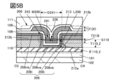
- 5A and 5B are plan and cross-sectional views illustrating a configuration example of a semiconductor device.
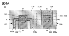
- 6A and 6B are plan views showing a configuration example of a semiconductor device.
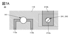
- 7A and 7B are plan views showing a configuration example of a semiconductor device.
- 8A to 8C are cross-sectional views showing configuration examples of a semiconductor device.
- Fig. 9A is a plan view showing a configuration example of a semiconductor device
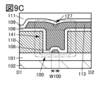
- Fig. 9B and Fig. 9C are cross-sectional views showing the configuration example of a semiconductor device.
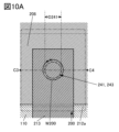
- 10A is a plan view showing a configuration example of a semiconductor device
- FIG. 10B is a cross-sectional view showing the configuration example of a semiconductor device.
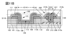
- 11A to 11C are cross-sectional views showing configuration examples of a semiconductor device.
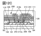
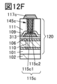
- 12A to 12F are cross-sectional views showing configuration examples of a semiconductor device.
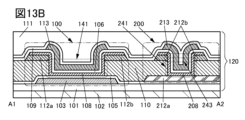
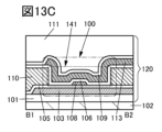
- Fig. 13A is a plan view showing a configuration example of a semiconductor device
- Fig. 13B and Fig. 13C are cross-sectional views showing the configuration example of a semiconductor device.
- FIG. 13A is a plan view showing a configuration example of a semiconductor device
- Fig. 13B and Fig. 13C are cross-sectional views showing the configuration example of a semiconductor device.
- FIG. 13A is a plan view showing a configuration example of
- FIG. 14 is a plan view showing a configuration example of a semiconductor device.
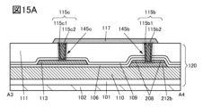
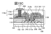
- 15A to 15C are cross-sectional views showing configuration examples of a semiconductor device.
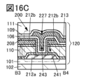
- 16A to 16C are cross-sectional views showing configuration examples of a semiconductor device.
- Fig. 17A is a plan view showing a configuration example of a semiconductor device, and Fig. 17B and Fig. 17C are cross-sectional views showing the configuration example of a semiconductor device.
- FIG. 18 is a plan view showing a configuration example of a semiconductor device.
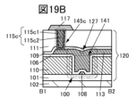
- 19A to 19C are cross-sectional views showing configuration examples of a semiconductor device.
- Fig. 20A is a block diagram showing a configuration example of a display device
- Fig. 20B is a plan view showing a configuration example of a pixel
- Fig. 20A is a block diagram showing a configuration example of a display device
- Fig. 20B is a plan view showing a configuration example of a pixel
- Fig. 20A is
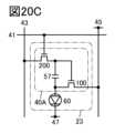
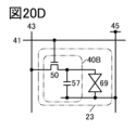
- 20C and Fig. 20D are circuit diagrams showing a configuration example of a pixel.
- 21A and 21B are plan views showing a configuration example of a semiconductor device.
- FIG. 22 is a cross-sectional view showing a configuration example of a semiconductor device.
- 23A and 23B are plan views showing a configuration example of a semiconductor device.
- FIG. 24 is a cross-sectional view showing a configuration example of a semiconductor device.
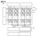
- Fig. 25A is a block diagram showing a configuration example of a display device
- Fig. 25B is a circuit diagram showing a configuration example of a pixel.
- FIG. 26 is a cross-sectional view showing a configuration example of a semiconductor device.
- 27A and 27B are plan views showing a configuration example of a semiconductor device.
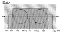
- 28A and 28B are plan views and a cross-sectional view showing a configuration example of a semiconductor device.
- 29A is a plan view showing a configuration example of a semiconductor device
- FIG 29B is a cross-sectional view showing the configuration example of a semiconductor device.
- FIG. 30 is a cross-sectional view showing a configuration example of a semiconductor device.
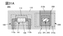
- 31A and 31B are plan views showing a configuration example of a semiconductor device.
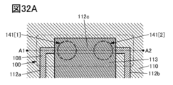
- 32A and 32B are plan views and a cross-sectional view showing a configuration example of a semiconductor device.
- 33A is a plan view showing a configuration example of a semiconductor device
- FIG 33B is a cross-sectional view showing the configuration example of a semiconductor device.
- 34A and 34B are cross-sectional views showing a configuration example of a semiconductor device.
- 35A and 35B are cross-sectional views showing a configuration example of a semiconductor device.
- 36A to 36C are cross-sectional views showing configuration examples of a semiconductor device.
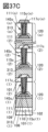
- 37A to 37C are cross-sectional views showing configuration examples of a semiconductor device.
- 38A to 38C are cross-sectional views showing an example of a method for manufacturing a semiconductor device.
- 39A and 39B are cross-sectional views showing an example of a method for manufacturing a semiconductor device.
- 40A and 40B are cross-sectional views showing an example of a method for manufacturing a semiconductor device.
- 41A and 41B are cross-sectional views showing an example of a method for manufacturing a semiconductor device.
- 42A and 42B are cross-sectional views showing an example of a method for manufacturing a semiconductor device.
- 43A to 43C are cross-sectional views showing an example of a method for manufacturing a semiconductor device.
- 44A and 44B are cross-sectional views showing an example of a method for manufacturing a semiconductor device.
- 45A and 45B are cross-sectional views showing an example of a method for manufacturing a semiconductor device.
- 46A and 46B are cross-sectional views showing an example of a method for manufacturing a semiconductor device.
- 47A and 47B are cross-sectional views showing an example of a method for manufacturing a semiconductor device.
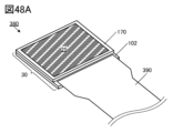
- 48A and 48B are perspective views showing a configuration example of a display device.
- FIG. 49 is a cross-sectional view showing a configuration example of a display device.
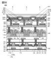
- FIG. 50 is a cross-sectional view showing a configuration example of a display device.
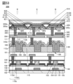
- FIG. 51 is a cross-sectional view showing an example of the configuration of a display device.
- FIG. 52 is a cross-sectional view showing a configuration example of a display device.
- FIG. 53 is a cross-sectional view showing a configuration example of a display device.
- FIG. 54 is a cross-sectional view showing an example of the configuration of a display device.
- Fig. 55A is a plan view showing a configuration example of a display device
- Fig. 55B and Fig. 55C are cross-sectional views showing the configuration example of the display device.
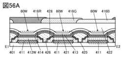
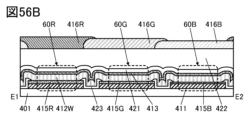
- 56A and 56B are cross-sectional views showing a configuration example of a display device.
- FIG. 57 is a cross-sectional view showing a configuration example of a display device.
- FIG. 58 is a cross-sectional view showing an example of the configuration of a display device.
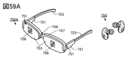
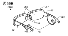
- 59A to 59D are diagrams showing configuration examples of electronic devices.
- 60A to 60F are diagrams showing configuration examples of electronic devices.
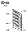
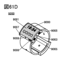
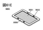
- 61A to 61G are diagrams showing configuration examples of electronic devices.
- ordinal numbers “first” and “second” are used for convenience and do not limit the number of components or the order of the components (e.g., the order of processes or the order of stacking).
- an ordinal number attached to a component in one part of this specification may not match an ordinal number attached to the same component in another part of this specification or in the claims.
- the terms “above,” “below,” “upward,” or “below” indicating position may be used for convenience in describing the positional relationship between components with reference to the drawings. Furthermore, the positional relationship between components changes as appropriate depending on the direction in which each configuration is depicted. Therefore, the terms are not limited to those described in this specification, and can be rephrased appropriately depending on the situation. For example, the expression “insulating layer located above a conductive layer” can be rephrased as “insulating layer located below a conductive layer” by rotating the orientation of the drawing shown by 180 degrees.
- the words “layer” and “film” may be interchangeable depending on the circumstances or situation.
- the term “conductive layer” may be changed to the term “conductive film.”
- the term “insulating layer” may be changed to the term “insulating film.”
- the term “semiconductor layer” may be changed to the term “semiconductor film.”
- a transistor is a type of semiconductor element that can perform functions such as amplifying current or voltage and switching operations that control conduction or non-conduction.
- transistor includes IGFETs (Insulated Gate Field Effect Transistors) and thin film transistors (TFTs).
- source and drain may be interchanged when transistors of different polarity are used, or when the direction of current changes during circuit operation. For this reason, in this specification and the like, the terms “source” and “drain” may be used interchangeably. Note that the source and drain of a transistor may be appropriately referred to as the source terminal and drain terminal, or the source electrode and drain electrode, etc., depending on the situation.
- Gate and backgate can be used interchangeably. For this reason, in this specification and the like, the terms “gate” and “backgate” can be used interchangeably. Note that the names of the gate and backgate of a transistor can be appropriately changed depending on the situation, such as gate electrode and backgate electrode.
- electrically connected includes cases where the connection is made via "something that has some kind of electrical action.”
- something that has some kind of electrical action is not particularly limited as long as it allows the transmission and reception of electrical signals between the objects to be connected.
- something that has some kind of electrical action includes electrodes or wiring, as well as switching elements such as transistors, resistive elements, coils, and other elements with various functions.
- off-state current refers to the current that flows between the source and drain when a transistor is in an off state (also called a non-conducting state or cut-off state).
- the off-state refers to a state in which the voltage between the gate and source is lower than the threshold voltage in an n-channel transistor (higher than the threshold voltage in a p-channel transistor).
- “voltage” often refers to the potential difference between a certain potential and a reference potential (for example, ground potential (GND potential) or source potential, etc.). Also, “potential” is relative, and the potential applied to wiring, for example, may change depending on the reference potential. Therefore, “voltage” and “potential” can sometimes be used interchangeably.
- a reference potential for example, ground potential (GND potential) or source potential, etc.
- potential is relative, and the potential applied to wiring, for example, may change depending on the reference potential. Therefore, “voltage” and “potential” can sometimes be used interchangeably.
- planar shapes roughly match means that at least a portion of the contours of the stacked layers overlap. For example, this includes cases where the upper and lower layers are processed using the same mask pattern, or parts of the same mask pattern. However, strictly speaking, the contours may not overlap, and the upper layer may be located inside the lower layer, or the upper layer may be located outside the lower layer, in which case it may also be said that the planar shapes roughly match. Furthermore, when the planar shapes match or roughly match, it can also be said that the ends are aligned or roughly aligned.
- planar shape of a certain component refers to the contour shape of the component when viewed in a plane.
- a planar view refers to a view from the normal direction of the surface on which the component is formed or the surface of the support (e.g., substrate) on which the component is formed.
- a tapered shape refers to a shape in which at least a portion of the side of the structure is inclined with respect to the substrate surface or the surface to be formed.
- the side of the structure, the substrate surface, and the surface to be formed do not necessarily need to be completely flat, and may be approximately planar with a slight curvature, or approximately planar with fine irregularities.
- a device fabricated using a metal mask or an FMM may be referred to as a device with an MM (metal mask) structure.
- a device fabricated without using a metal mask or an FMM may be referred to as a device with an MML (metal maskless) structure.
- MML metal maskless
- a device with an MML structure can be fabricated without using a metal mask, it is possible to exceed the upper limit of the definition caused by the alignment accuracy of the metal mask.
- a device with an MML structure can eliminate the need for equipment related to fabricating a metal mask and a process for cleaning the metal mask.
- a device with an MML structure is suitable for mass production because it is possible to keep fabrication costs low.
- SBS Side By Side
- the SBS structure allows the materials and configuration to be optimized for each light-emitting element, which increases the freedom to select materials and configurations and makes it easier to improve brightness and reliability.
- holes or electrons may be referred to as “carriers”.
- the hole injection layer or electron injection layer may be referred to as the "carrier injection layer”
- the hole transport layer or electron transport layer may be referred to as the “carrier transport layer”
- the hole block layer or electron block layer may be referred to as the "carrier block layer”.
- the above-mentioned carrier injection layer, carrier transport layer, and carrier block layer may not be clearly distinguishable from each other depending on their cross-sectional shapes or characteristics.
- one layer may have two or three functions among the carrier injection layer, carrier transport layer, and carrier block layer.
- the light-emitting element has an EL layer between a pair of electrodes.
- the EL layer has at least a light-emitting layer.
- layers also called functional layers
- the EL layer has include a light-emitting layer, a carrier injection layer (hole injection layer and electron injection layer), a carrier transport layer (hole transport layer and electron transport layer), and a carrier block layer (hole block layer and electron block layer).
- the light-receiving element also called a light-receiving device
- one of the pair of electrodes may be referred to as a pixel electrode, and the other as a common electrode.
- the sacrificial layer (which may also be referred to as a mask layer) is located at least above the light-emitting layer (more specifically, the layer that is processed into an island shape among the layers that make up the EL layer) and has the function of protecting the light-emitting layer during the manufacturing process.
- an island-like light-emitting layer refers to a state in which the light-emitting layer is physically separated from the adjacent light-emitting layer.
- step discontinuity refers to the phenomenon in which a layer, film, or electrode is divided due to the shape of the surface on which it is formed (e.g., a step, etc.).
- an insulating layer that functions as a spacer is provided on a base insulating layer.
- the insulating layer that functions as a spacer may be simply referred to as a spacer, but the spacer may be read as an insulating layer.
- the spacer has a first opening that reaches the base insulating layer.
- a first transistor is provided so as to have a region located inside the first opening.
- a source electrode (first source electrode) and a drain electrode (first drain electrode) of the first transistor are provided on the spacer.
- the first source electrode and the first drain electrode are provided to face each other across the first opening in a plan view.
- the first semiconductor layer is provided so as to have a region located inside the first opening.
- the first semiconductor layer is provided with a channel formation region of the first transistor.
- the first semiconductor layer can be provided along the bottom surface and side surface of the first opening.
- the first semiconductor layer can have, for example, a region in contact with the top surface of the first source electrode, a region in contact with the side surface of the first source electrode, a region in contact with the top surface of the first drain electrode, and a region in contact with the side surface of the first drain electrode.
- a gate insulating layer and a gate electrode (first gate electrode) of the first transistor are provided in this order so as to have a region located inside the first opening.
- the first gate electrode is provided so as to have a region overlapping with the first semiconductor layer through the gate insulating layer inside the first opening.
- the first gate electrode is also provided so as to have a region facing the first semiconductor layer with the gate insulating layer sandwiched between them inside the first opening.
- the top surface of A exposed by the opening is referred to as the bottom surface of the opening.
- the side surface of B exposed by the opening is referred to as the side surface of the opening.
- the channel length can be set not only in the direction along the bottom surface of the first opening (also referred to as the horizontal direction) but also in the direction along the side surface of the first opening (also referred to as the vertical direction) in the first semiconductor layer.
- the channel length of the first transistor can be increased without increasing the area occupied by the first transistor, specifically, the area occupied by the first semiconductor layer, compared to the case where the first opening is not provided and, for example, a planar type transistor is used. Therefore, a transistor with a small size and high saturation can be realized.
- the saturation of the driving transistor that controls the current flowing to the light-emitting element can be increased while miniaturizing the pixel. Therefore, the current flowing to the light-emitting element can be stabilized, and the light emission luminance of the light-emitting element can be stabilized.
- the occurrence of variation over time in the current flowing to the light-emitting element can be suppressed, and the occurrence of variation over time in the light emission luminance of the light-emitting element can be suppressed.
- a second transistor having a different configuration from the first transistor can be provided on the base insulating layer.
- the first transistor and the second transistor can be formed using some of the same processes.
- a first conductive layer that functions as one of the source electrode (second source electrode) and drain electrode (second drain electrode) of the second transistor is provided on a base insulating layer.
- the spacer is provided on the first conductive layer.
- the spacer has a second opening that reaches the first conductive layer.
- the second opening can be formed in the same process as the first opening.
- a second transistor is provided so as to have a region located inside the second opening.
- a second conductive layer that functions as the other of the second source electrode and the second drain electrode is provided on the spacer.
- the second conductive layer has a third opening that has an area that overlaps with the second opening.
- the second conductive layer can be formed in the same process using the same material as the first source electrode and the first drain electrode.
- the first source electrode, the first drain electrode, and the second conductive layer can be formed by processing the same conductive film.
- the second semiconductor layer is provided so as to have a region located inside the second opening and a region located inside the third opening.
- the second semiconductor layer is provided with a channel formation region in the second transistor.
- the second semiconductor layer can be provided along the side surface of the spacer in the second opening and the side surface of the second conductive layer in the third opening.
- the second semiconductor layer can have, for example, a region in contact with the top surface of the first conductive layer, the side surface of the second conductive layer, and the top surface of the second conductive layer.
- the second semiconductor layer can be formed in the same process using the same material as the first semiconductor layer.
- the first semiconductor layer and the second semiconductor layer can be formed by processing the same semiconductor film.
- a gate insulating layer and a gate electrode (second gate electrode) of the second transistor are provided in this order on the second semiconductor layer so as to have a region located inside the second opening.
- the second gate electrode is provided inside the second opening so as to have a region facing the second semiconductor layer with the gate insulating layer sandwiched therebetween.
- the gate insulating layer of the second transistor can be shared with the gate insulating layer of the first transistor.
- the second gate electrode can be formed in the same process using the same material as the first gate electrode.
- the first gate electrode and the second gate electrode can be formed by processing the same conductive film.
- the channel length is along the side surface (also referred to as the vertical direction) of the second opening of the spacer, but not in the direction parallel to the top surface of the base insulating layer. Therefore, the channel length of the second transistor is shorter than that of the first transistor. Therefore, the second transistor can have a larger on-state current than the first transistor. Therefore, by applying the second transistor to a selection transistor provided in the above-mentioned pixel, for example, a selection transistor having a function of selecting a pixel to which image data is written, the display device of one embodiment of the present invention can be driven at high speed.
- parallel refers to a state in which two straight lines are arranged at an angle of -10° or more and 10° or less. Therefore, it also includes cases in which the angle is -5° or more and 5° or less.
- substantially parallel or “roughly parallel” refers to a state in which two straight lines are arranged at an angle of -30° or more and 30° or less.
- perpendicular refers to a state in which two straight lines are arranged at an angle of 80° or more and 100° or less. Therefore, it also includes cases in which the angle is 85° or more and 95° or less.
- substantially perpendicular or “approximately perpendicular” refers to a state in which two straight lines are arranged at an angle of 60° or more and 120° or less.
- the semiconductor device of one embodiment of the present invention for example, multiple transistors with different electrical characteristics can be formed by sharing some of the steps. Therefore, it is possible to easily realize, for example, a circuit having desired performance while suppressing manufacturing costs. As described above, a semiconductor device having low cost and high performance can be realized. For example, when the semiconductor device of one embodiment of the present invention is applied to a display device, a display device that is low cost, has high definition, has high reliability, and operates at high speed can be realized.
- the first source electrode, the first drain electrode, and the second conductive layer, and the first and second semiconductor layers can be formed using the same mask pattern.
- a conductive film is formed on a spacer, and the third opening and the fourth opening that reach the spacer are formed in the conductive film.
- a first opening that has an area overlapping with the fourth opening and reaches the base insulating layer, and a second opening that has an area overlapping with the third opening and reaches the first conductive layer are formed in the spacer.
- a semiconductor film is formed so as to cover the first to fourth openings.
- a resist mask reflecting the mask pattern is formed using a photolithography method, and the first semiconductor layer and the second semiconductor layer are formed by processing the semiconductor film based on the mask pattern.
- the conductive film is processed based on the same mask pattern to form the first source electrode, the first drain electrode, and the second conductive layer.
- the semiconductor film and the conductive film can be processed using, for example, an etching method.
- the manufacturing cost of the semiconductor device of one embodiment of the present invention can be reduced. Therefore, the semiconductor device of one embodiment of the present invention can be a low-cost semiconductor device.
- the end of the first semiconductor layer, specifically the bottom end, outside the first opening can have a region that coincides or roughly coincides with the end of the first source electrode, specifically the top end, and a region that coincides or roughly coincides with the end of the first drain electrode, specifically the top end.
- the end of the second semiconductor layer, specifically the bottom end, outside the third opening can have a region that coincides or roughly coincides with the end of the second conductive layer, specifically the top end.
- the lower surface end of the first semiconductor layer outside the first opening may not coincide with the upper surface end of the first source electrode and the upper surface end of the first drain electrode.
- the lower surface end of the second semiconductor layer outside the third opening may not coincide with the upper surface end of the second conductive layer. Even in such a case, it can be said that the lower surface end of the first semiconductor layer outside the first opening roughly coincides with the upper surface end of the first source electrode and the upper surface end of the first drain electrode. Also, it can be said that the lower surface end of the second semiconductor layer outside the third opening roughly coincides with the upper surface end of the second conductive layer.
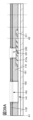
- Fig. 1A is a plan view showing a configuration example of a semiconductor device 20 which is a semiconductor device according to one embodiment of the present invention.
- some of the components of the semiconductor device 20 for example, some insulating layers, are omitted.
- some of the components are omitted from the plan views showing the configuration example of the semiconductor device in the following drawings.
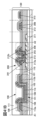
- Fig. 1B is a plan view in which some of the components are omitted from Fig. 1A.
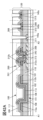
- Fig. 2A is a plan view in which some of the components are omitted from Fig. 1B.
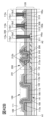
- Fig. 2B is a plan view in which the insulating layers shown in Fig. 2A are indicated by dotted lines.
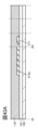
- Figure 3A is a cross-sectional view of the cut surface taken along dashed line A1-A2 in Figure 1A.
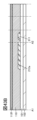
- Figure 3B is a cross-sectional view of the cut surface taken along dashed line B1-B2 in Figure 1A.
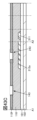
- Figure 3C is a cross-sectional view of the cut surface taken along dashed line B3-B4 in Figure 1A.
- an insulating layer 101 is provided on a substrate 102, and an insulating layer 110, a transistor 100, and a transistor 200 are provided on the insulating layer 101.
- the insulating layer 101 functions as a base insulating layer.
- the insulating layer 110 functions as a spacer. Note that at least one of an electrode, a wiring, a transistor, a capacitance, a resistor, and the like may be provided between the substrate 102 and the insulating layer 101.
- a base insulating layer may be provided on the substrate 102, a layer in which wiring is provided (also referred to as a wiring layer) may be provided on the base insulating layer, and the insulating layer 101 may be provided on the wiring layer.
- the transistor 100 has a conductive layer 113, a conductive layer 112a, a conductive layer 112b, an insulating layer 106, and a semiconductor layer 108.
- the conductive layer 113 functions as a gate electrode
- a part of the insulating layer 106 functions as a gate insulating layer.
- the conductive layer 112a functions as one of the source electrode and the drain electrode
- the conductive layer 112b functions as the other of the source electrode and the drain electrode.
- Each layer constituting the transistor 100 may have a single-layer structure or a stacked structure.
- the insulating layer 110 has an opening 141 that reaches the insulating layer 101.
- the transistor 100 is provided so as to have a region located inside the opening 141.
- Conductive layers 112a and 112b are provided on the insulating layer 110.
- two conductive layers 112 are provided on the insulating layer 110 for each transistor 100.
- the conductive layers with alphabetical characters added to the reference numeral "112" may be collectively referred to as conductive layer 112.
- the ends of the conductive layer 112a and a part of the conductive layer 112b coincide or roughly coincide with the end of the insulating layer 110 in the opening 141.
- the upper surface end of the insulating layer 110 in the opening 141 has a region that coincides or roughly coincides with the lower surface end of the conductive layer 112a that faces the opening 141 in a plan view, and a region that coincides or roughly coincides with the lower surface end of the conductive layer 112b that faces the opening 141 in a plan view. This makes it easier to control, for example, the channel length of the transistor 100, and makes it easier to make the transistor 100 into a transistor having desired electrical characteristics.
- the conductive layer 112a and the conductive layer 112b can be formed using the same material.
- the conductive layer 112a and the conductive layer 112b can be formed in the same process. For example, a conductive film that will become the conductive layer 112a and the conductive layer 112b is formed, and the conductive film is processed to form the conductive layer 112a and the conductive layer 112b.
- the semiconductor layer 108 has a region located inside the opening 141.
- the semiconductor layer 108 can be provided along the bottom and side surfaces of the opening 141.
- the semiconductor layer 108 can also have, for example, a region in contact with the top surface of the conductive layer 112a, a region in contact with the side surface of the conductive layer 112a, a region in contact with the top surface of the conductive layer 112b, and a region in contact with the side surface of the conductive layer 112b.
- the semiconductor layer 108 can have a region in contact with the top surface of the insulating layer 101 and a region in contact with the side surface of the insulating layer 110.
- the region of the semiconductor layer 108 in contact with the conductive layer 112a functions as one of the source region and the drain region, and the region in contact with the conductive layer 112b functions as the other of the source region and the drain region.
- a channel formation region is provided between the source region and the drain region.
- FIG. 1B is a diagram in which the conductive layer 113 is omitted from FIG. 1A.
- the end of the semiconductor layer 108, specifically the bottom end, outside the opening 141 has an area that coincides or roughly coincides with the end of the conductive layer 112a, specifically the top end, and an area that coincides or roughly coincides with the end of the conductive layer 112b, specifically the top end.
- the bottom end of the semiconductor layer 108 can have an area that coincides or roughly coincides with the top end of the conductive layer 112a, and an area that coincides or roughly coincides with the top end of the conductive layer 112b.
- a conductive film is formed on the insulating layer 110, and an opening is formed in the conductive film that reaches the insulating layer 110.
- an opening 141 is formed in the insulating layer 110, which has an area overlapping with the opening and reaches the insulating layer 101.
- a semiconductor film is formed so as to cover the opening 141.
- a resist mask reflecting a mask pattern is formed using photolithography, and the semiconductor film is processed based on the mask pattern to form the semiconductor layer 108.
- the conductive film is processed based on the same mask pattern, so that the conductive layer 112a and the conductive layer 112b can be formed.
- the semiconductor film and the conductive film can be processed by, for example, an etching method.
- the number of manufacturing steps of the transistor 100 can be reduced compared to the case where, for example, after the conductive film is formed and before the semiconductor film is formed, the conductive film is processed to form the conductive layers 112a and 112b, and then a semiconductor film is formed and processed to form the semiconductor layer 108. Therefore, the manufacturing cost of the semiconductor device 20 can be reduced. Therefore, the semiconductor device 20 can be a low-cost semiconductor device.
- the bottom end of the semiconductor layer 108 outside the opening 141 may not coincide with the top end of the conductive layer 112a and the top end of the conductive layer 112b. Even in such a case, it can be said that the bottom end of the semiconductor layer 108 outside the opening 141 roughly coincides with the top end of the conductive layer 112a and the top end of the conductive layer 112b.
- FIG. 2A is a diagram in which the semiconductor layer 108 is further omitted from FIG. 1B.
- FIG. 2B is a diagram in which the insulating layer 110 shown in FIG. 2A is shown by a dotted line.
- the conductive layer 112a and the conductive layer 112b are provided so as to face each other via the opening 141 in a plan view.
- the insulating layer 106 is provided to have a region located inside the opening 141, specifically, to cover the opening 141.
- the insulating layer 106 is provided on the semiconductor layer 108, the insulating layer 110, and the insulating layer 101.
- the insulating layer 106 has a shape along the top and side surfaces of the semiconductor layer 108, the side surfaces of the conductive layers 112a and 112b, the top and side surfaces of the insulating layer 110, and the top surface of the insulating layer 101.
- the insulating layer 106 can have a region in contact with the top surface of the semiconductor layer 108, a region in contact with the side surface of the semiconductor layer 108, a region in contact with the side surface of the conductive layer 112a, a region in contact with the side surface of the conductive layer 112b, a region in contact with the top surface of the insulating layer 110, a region in contact with the side surface of the insulating layer 110, and a region in contact with the top surface of the insulating layer 101.
- the conductive layer 113 is provided on the insulating layer 106 so as to have a region located inside the opening 141.
- the conductive layer 113 can have a first region located outside the opening 141 and a second region overlapping the opening 141.
- the conductive layer 113 is provided so as to have a region overlapping the semiconductor layer 108 via the insulating layer 106 in the second region.
- the conductive layer 113 is also provided so as to have a region facing the semiconductor layer 108 with the insulating layer 106 sandwiched between them inside the opening 141.
- the conductive layer 113 has a shape that follows the insulating layer 106, and specifically, can have a shape that follows the top surface of the insulating layer 106 and the side surface of the insulating layer 106 inside the opening 141.
- the conductive layer 113 can also have a region that contacts the top surface of the insulating layer 106 and a region that contacts the side surface of the insulating layer 106 inside the opening 141.
- the transistor 200 has a conductive layer 213, a conductive layer 212a, a conductive layer 212b, an insulating layer 106, and a semiconductor layer 208.
- the conductive layer 213 functions as a gate electrode
- a part of the insulating layer 106 functions as a gate insulating layer.
- the conductive layer 212a functions as one of the source electrode and the drain electrode
- the conductive layer 212b functions as the other of the source electrode and the drain electrode.
- Each layer constituting the transistor 200 may have a single-layer structure or a stacked structure.
- the conductive layer 213 is omitted from FIG. 1A.
- the semiconductor layer 208 is further omitted from FIG. 1B.
- the conductive layer 212a is provided on the insulating layer 101.
- the insulating layer 110 is provided on the conductive layer 212a.
- the insulating layer 110 is provided so as to cover the upper surface and side surfaces of the conductive layer 212a.
- the insulating layer 110 has an opening 241 that reaches the conductive layer 212a.
- the transistor 200 is provided so as to have a region located inside the opening 241. Note that although an example in which the insulating layer 110 is planarized is shown in FIG. 3A and FIG. 3C, the insulating layer 110 does not have to be planarized.
- a conductive layer 212b is provided on the insulating layer 110.
- the conductive layer 212b has an opening 243 having an area overlapping with the opening 241.
- the planar shapes of the opening 241 and the opening 243 can be the same as the planar shape that the opening 141 can have.
- the planar shapes of the opening 241 and the opening 243 can be made to match or approximately match each other. In this case, it is preferable that the lower surface end of the opening 243 of the conductive layer 212b matches or approximately matches the upper surface end of the opening 241 of the insulating layer 110.
- openings 241 and 243 do not have to be the same. When the planar shapes of openings 241 and 243 are circular, openings 241 and 243 may or may not be concentric.
- the conductive layer 212b can be formed using the same material as the conductive layer 112a and the conductive layer 112b.
- the conductive layer 212b can be formed in the same process as the conductive layer 112a and the conductive layer 112b. For example, a conductive film that will become the conductive layer 112a, the conductive layer 112b, and the conductive layer 212b is formed, and the conductive film is processed to form the conductive layer 112a, the conductive layer 112b, and the conductive layer 212b.
- the semiconductor layer 208 has a region located inside the opening 241 and a region located inside the opening 243.
- the semiconductor layer 208 can be provided along the bottom and side surfaces of the opening 241 and the side surfaces of the opening 243.
- the semiconductor layer 208 can have, for example, a region in contact with the top surface of the conductive layer 212a, a region in contact with the side surface of the conductive layer 212b, and a region in contact with the top surface of the conductive layer 212b.
- the semiconductor layer 208 can have a region in contact with the side surface of the insulating layer 110.
- the region of the semiconductor layer 208 in contact with the conductive layer 212a functions as one of the source region and the drain region, and the region in contact with the conductive layer 212b functions as the other of the source region and the drain region.
- a channel formation region is provided between the source region and the drain region.
- the semiconductor layer 208 can be formed using the same material as the semiconductor layer 108.
- the semiconductor layer 208 can be formed in the same process as the semiconductor layer 108.
- the semiconductor layer 108 and the semiconductor layer 208 can be formed by forming a semiconductor film that will become the semiconductor layer 108 and the semiconductor layer 208, and processing the semiconductor film.
- the end of the semiconductor layer 208 has an area that coincides or roughly coincides with the end of the conductive layer 212b, specifically the top end.
- the bottom end of the semiconductor layer 208 can have an area that coincides or roughly coincides with the top end of the conductive layer 212b.
- a conductive film is formed on the insulating layer 110, and in addition to the aforementioned opening that reaches the insulating layer 110, an opening 243 that reaches the conductive layer 212a is formed in the conductive film.
- an opening 241 that has an area that overlaps with the opening 243 and reaches the conductive layer 212a is formed in the insulating layer 110.
- the opening 241 can be formed in the same process as the opening 141.
- a semiconductor film is formed so as to cover the opening 141, the opening 241, and the opening 243.
- a resist mask reflecting a mask pattern is formed by photolithography, and the semiconductor film is processed based on the mask pattern to form the semiconductor layer 108 and the semiconductor layer 208.
- the conductive film is processed based on the same mask pattern to form the conductive layer 112a, the conductive layer 112b, and the conductive layer 212b.
- the semiconductor film and the conductive film can be processed by, for example, an etching method.
- the number of manufacturing steps for the transistor 200 can be reduced compared to, for example, forming the conductive layer 212b by processing the conductive film after the formation of the conductive film and before the formation of the semiconductor film, and then forming and processing the semiconductor film to form the semiconductor layer 208.
- the manufacturing cost of the semiconductor device 20 can be reduced as described above. Therefore, the semiconductor device 20 can be a low-cost semiconductor device.
- the etching rate of the semiconductor film and the etching rate of the conductive film may differ.
- the bottom edge of the semiconductor layer 208 outside the opening 243 may not coincide with the top edge of the conductive layer 212b. Even in such a case, it can be said that the bottom edge of the semiconductor layer 208 outside the opening 243 roughly coincides with the top edge of the conductive layer 212b.
- the insulating layer 106 is provided to have a region located inside the opening 241 and a region located inside the opening 243, specifically, the insulating layer 106 is provided to cover the opening 241 and the opening 243.
- the insulating layer 106 is provided on the semiconductor layer 208.
- the insulating layer 106 has a shape that follows the top surface and side surface of the semiconductor layer 208 and the side surface of the conductive layer 212b.
- the insulating layer 106 can have a region in contact with the top surface of the semiconductor layer 208, a region in contact with the side surface of the semiconductor layer 208, and a region in contact with the side surface of the conductive layer 212b.
- the conductive layer 213 is provided on the insulating layer 106 so as to have a region located inside the opening 241 and a region located inside the opening 243.
- the conductive layer 213 can have a third region located outside the opening 241 and a fourth region overlapping the opening 241.
- the third region can be a region located outside the opening 243
- the fourth region can be a region overlapping the opening 243.
- the conductive layer 213 is provided inside the opening 241 so as to have a region that faces the semiconductor layer 208 with the insulating layer 106 sandwiched between them.
- the conductive layer 213 has a shape that conforms to the insulating layer 106, specifically, the top surface of the insulating layer 106 and the side surfaces of the insulating layer 106 inside the openings 241 and 243.
- the conductive layer 213 can also have a region that contacts the top surface of the insulating layer 106 and a region that contacts the side surfaces of the insulating layer 106 inside the openings 241 and 243.
- the conductive layer 213 can be formed using the same material as the conductive layer 113.
- the conductive layer 213 can be formed in the same process as the conductive layer 113.
- the conductive layer 113 and the conductive layer 213 can be formed by forming a conductive film that will become the conductive layer 113 and the conductive layer 213 and processing the conductive film.
- the transistor 200 is a so-called top-gate transistor that has a gate electrode above the semiconductor layer 208. Furthermore, since the bottom surface of the semiconductor layer 208 is in contact with the conductive layer 212a and the conductive layer 212b that function as a source electrode and a drain electrode, the transistor 200 can be called a TGBC (Top Gate Bottom Contact) type transistor.
- TGBC Top Gate Bottom Contact
- the transistor 200 can have a source electrode, a layer having a channel formation region, and a drain electrode stacked on top of each other, the area occupied can be significantly reduced compared to a so-called planar type transistor in which the layer having the channel formation region is arranged in a planar shape.
- the conductive layers 212a, 212b, and 213 can each function as wiring, and the transistor 200 can be provided in a region where these wirings overlap. That is, in a circuit having the transistor 200 and the wiring, the area occupied by the transistor 200 and the wiring can be reduced. Therefore, the area occupied by the circuit can be reduced, and a small-sized semiconductor device can be obtained. Note that the conductive layers 112a, 112b, and 113 of the transistor 100 can also each function as wiring.
- the conductive layer 112a which functions as one of the source and drain electrodes of the transistor 100, and the conductive layer 112b, which functions as the other of the source and drain electrodes of the transistor 100, are provided on the same surface. Specifically, the conductive layer 112a and the conductive layer 112b are provided on the insulating layer 110. On the other hand, the conductive layer 212a, which functions as one of the source and drain electrodes of the transistor 200, and the conductive layer 212b, which functions as the other of the source and drain electrodes of the transistor 200, are provided on different surfaces.
- the conductive layer 212a is provided on the insulating layer 101
- the conductive layer 212b is provided on the insulating layer 110
- the insulating layer 110 is sandwiched between the conductive layer 212a and the conductive layer 212b. It can also be said that one of the source electrode and drain electrode of transistor 200 is provided on a different surface from the source electrode and drain electrode of transistor 100, and the other of the source electrode and drain electrode of transistor 200 is provided on the same surface as the source electrode and drain electrode of transistor 100.
- the semiconductor device of one embodiment of the present invention when the semiconductor device of one embodiment of the present invention is applied to a pixel circuit of a display device, the area occupied by the pixel circuit can be reduced, and a high-definition display device can be obtained.
- the semiconductor device of one embodiment of the present invention when the semiconductor device of one embodiment of the present invention is applied to a driver circuit of a display device (e.g., one or both of a scanning line driver circuit and a signal line driver circuit), the area occupied by the driver circuit can be reduced, and a display device with a narrow frame can be obtained.
- An insulating layer 109 is provided to cover the transistor 100 and the transistor 200.
- the insulating layer 109 is provided over the conductive layer 113, the conductive layer 213, and the insulating layer 106.
- the insulating layer 109 functions as a protective layer for the transistor 100 and the transistor 200.
- An insulating layer 111 is provided on the insulating layer 109.
- the insulating layer 111 functions as an interlayer insulating layer. Although an example in which the insulating layer 111 is planarized is shown in FIG. 3A, FIG. 3B, and FIG. 3C, the insulating layer 111 does not have to be planarized.
- the insulating layer 109 may also be planarized.
- the insulating layers 101 to 111 are collectively referred to as layer 120.
- the transistor 100 and the transistor 200 are provided in layer 120.
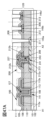
- Figure 3D is a cross-sectional view showing a conductive layer 311 provided in the same layer as the conductive layer 212a, a conductive layer 117a provided on the insulating layer 111 and functioning as wiring, and a plug 115a electrically connecting them.
- the conductive layer 311 is provided on the insulating layer 101
- the insulating layer 110 is provided on the insulating layer 101 and the conductive layer 311.
- the conductive layer 311 can be the conductive layer 212a itself.
- the conductive layer 311 can be a wiring different from the conductive layer 212a that is formed using the same material and in the same process as the conductive layer 212a.
- the insulating layer 110, the insulating layer 106, the insulating layer 109, and the insulating layer 111 have an opening 145a that reaches the conductive layer 311, and a plug 115a is provided to fill the opening 145a.
- the conductive layer 311 and the conductive layer 117a are electrically connected via the plug 115a.
- the plug 115a has a conductive layer 115a1 provided along the side and bottom surface of the opening 145a, and a conductive layer 115a2 located inside the opening 145a from the conductive layer 115a1 and provided to fill the opening 145a. Note that since the insulating layer 110, the insulating layer 106, the insulating layer 109, and the insulating layer 111 are provided in the layer 120, the plug 115a is also provided in the layer 120.
- the conductive layer 115a1 is preferably made of a conductive material through which hydrogen and oxygen do not easily diffuse.
- a conductive material through which hydrogen and oxygen do not easily diffuse.
- tantalum, tantalum nitride, titanium, titanium nitride, ruthenium, ruthenium oxide, or the like is preferably used.
- a conductive material that has the function of suppressing the permeation of impurities such as water and hydrogen may be used in a single layer or a stacked layer. With this structure, impurities such as water and hydrogen can be suppressed from entering the semiconductor layer 108 and the semiconductor layer 208 through the plug 115a.
- the conductive layer 115a2 may be made of a conductive material mainly composed of tungsten, copper, or aluminum.
- 3E is a cross-sectional view showing a conductive layer 312 provided in the same layer as the conductive layer 112a, the conductive layer 112b, and the conductive layer 212b, a semiconductor layer 308 provided in the same layer as the semiconductor layer 108 and the semiconductor layer 208, a conductive layer 117b provided on the insulating layer 111 and functioning as wiring, and a plug 115b electrically connecting the conductive layer 312 and the conductive layer 117b.
- the conductive layer 312 is provided on the insulating layer 110
- the semiconductor layer 308 is provided on the conductive layer 312
- the insulating layer 106 is provided on the insulating layer 110 and the semiconductor layer 308.
- the conductive layer 312 can be the conductive layer 112a itself, the conductive layer 112b itself, or the conductive layer 212b itself, and the semiconductor layer 308 can be the semiconductor layer 108 itself or the semiconductor layer 208 itself.
- the conductive layer 312 can be a wiring different from the conductive layer 112a, the conductive layer 112b, and the conductive layer 212b, which is formed using the same material and in the same process as the conductive layer 112a, the conductive layer 112b, and the conductive layer 212b.
- the semiconductor layer 308 can be a semiconductor layer different from the semiconductor layer 108 and the semiconductor layer 208, which is formed using the same material and in the same process as the semiconductor layer 108 and the semiconductor layer 208.
- the conductive layers 112a, 112b, and 212b, and the semiconductor layers 108 and 208 can be formed using the same mask pattern.
- the conductive layer 312 and the semiconductor layer 308 can also be formed using the same mask pattern. Therefore, the end of the semiconductor layer 308, specifically the end of the lower surface, can have an area that coincides with or roughly corresponds to the end of the conductive layer 312, specifically the end of the upper surface.
- the semiconductor layer 308, the insulating layer 106, the insulating layer 109, and the insulating layer 111 have an opening 145b that reaches the conductive layer 312, and a plug 115b is provided to fill the opening 145b.
- the conductive layer 312 and the conductive layer 117b are electrically connected through the plug 115b.
- the plug 115b has a conductive layer 115b1 provided along the side and bottom surface of the opening 145b, and a conductive layer 115b2 located inside the opening 145b from the conductive layer 115b1 and provided to fill the opening 145b.
- the conductive layer 115b1 can be made of the same material as the material that can be used for the conductive layer 115a1 described above.
- the conductive layer 115b2 can be made of the same material as the material that can be used for the conductive layer 115a2 described above. Since the semiconductor layer 308, the insulating layer 106, the insulating layer 109, and the insulating layer 111 are provided in the layer 120, the plug 115b is also provided in the layer 120.
- 3F is a cross-sectional view showing the conductive layer 113, the conductive layer 313 provided in the same layer as the conductive layer 213, the conductive layer 117c provided on the insulating layer 111 and functioning as wiring, and the plug 115c electrically connecting them.
- the conductive layer 313 is provided on the insulating layer 106
- the insulating layer 109 is provided on the insulating layer 106 and the conductive layer 313.
- the conductive layer 313 can be the conductive layer 113 itself or the conductive layer 213 itself.
- the conductive layer 313 can be a wiring different from the conductive layer 113 and the conductive layer 213, formed using the same material as the conductive layer 113 and the conductive layer 213, and formed in the same process.
- the insulating layer 109 and the insulating layer 111 have an opening 145c that reaches the conductive layer 313, and a plug 115c is provided to fill the opening 145c.
- the conductive layer 313 and the conductive layer 117c are electrically connected through the plug 115c.
- the plug 115c preferably has a conductive layer 115c1 provided along the side and bottom of the opening 145c, and a conductive layer 115c2 located inside the opening 145c from the conductive layer 115c1 and provided to fill the opening 145c.
- the conductive layer 115c1 can be made of a material similar to the material that can be used for the conductive layer 115a1 described above.
- the conductive layer 115c2 can be made of a material similar to the material that can be used for the conductive layer 115a2 described above. Note that the insulating layer 109 and the insulating layer 111 are provided in the layer 120, and therefore the plug 115c is also provided in the layer 120.
- plug 115a when matters common to plug 115a, plug 115b, and plug 115c are described, the symbols added to the reference numerals may be omitted and the description may be written as plug 115.
- conductive layer 117a, conductive layer 117b, and conductive layer 117c may also be described as conductive layer 117.
- opening 145a, opening 145b, and opening 145c may also be described as opening 145.
- the conductive layer 117 may be a single layer or a multi-layer structure of a material that can be used for at least one of the conductive layers 311, 312, 313, and the plug 115.
- the conductive layer 117 may have a five-layer structure in which a layer using titanium, a layer using titanium nitride, a layer using aluminum, a layer using titanium, and a layer using titanium nitride are stacked in this order.
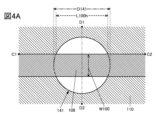
- Figure 4A is an enlarged view of the opening 141 shown in Figure 1B and the area nearby.
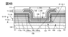
- Figure 4B is a cross-sectional view of the cut surface taken along C1-C2 in Figure 4A.
- Figure 4C is a cross-sectional view of the cut surface taken along dashed line D1-D2 in Figure 4A. The channel length, channel width, etc. of the transistor 100 will be described with reference to Figures 4A to 4C.
- the channel length of the transistor 100 is length L100
- the channel width is width W100
- the width of the opening 141 is width D141
- the thickness of the insulating layer 110 is thickness T110_1
- the angle between the side surface of the opening 141 of the insulating layer 110 and the upper surface of the insulating layer 101 is angle ⁇ 110_1.
- the length L100, width W100, width D141, and thickness T110_1 are indicated by double-headed arrows. The same notation is used in other drawings.
- the thickness T110_1 can be the shortest distance between the surface on which the insulating layer 110 is formed (here, the upper surface of the insulating layer 101) and the lower surface of the conductive layer 112a or the conductive layer 112b in a cross-sectional view, as shown in FIG. 4B.
- the regions of the semiconductor layer 108 are region 108i, region 108na, and region 108nb. Region 108i is provided between region 108na and region 108nb.
- the region 108na is a region in contact with the conductive layer 112a of the semiconductor layer 108 and a region in its vicinity. At least a part of the region 108na functions as one of the source region and the drain region of the transistor 100.
- the region 108nb is a region in contact with the conductive layer 112b of the semiconductor layer 108 and a region in its vicinity. At least a part of the region 108nb functions as the other of the source region and the drain region of the transistor 100.
- At least a part of the region 108na and the region 108nb can be regions having lower electrical resistance than at least a part of the region 108i (hereinafter, also referred to as low resistance regions).
- at least a part of the region 108na and the region 108nb can be regions having a higher carrier concentration or a higher oxygen defect density than at least a part of the region 108i.
- 4B shows an example in which the height of the boundary between region 108i and region 108na matches or roughly matches the height of the boundary between insulating layer 110 and conductive layer 112a, and the height of the boundary between region 108i and region 108nb matches or roughly matches the height of the boundary between insulating layer 110 and conductive layer 112b, but these heights do not have to match or roughly match.
- the heights are the same or approximately the same.
- a reference surface e.g., a flat surface such as a substrate surface
- a planarization process may be performed to expose the surface of a single layer or multiple layers.
- the surface to be processed in the planarization process has the same height from the reference surface.
- the heights of the multiple layers may not be strictly the same depending on the processing device, processing method, or material of the surface to be processed during the planarization process. In this specification, this case is also referred to as "the heights are the same or approximately the same”.
- the difference between the height of the top surface of the first layer and the height of the top surface of the second layer is 20 nm or less, it is also referred to as "the heights are the same or approximately the same".
- the length L100 which is the channel length of the transistor 100, corresponds to the sum of twice the length of the side of the opening 141 of the insulating layer 110 in a cross-sectional view and the length L100h, which is the shortest value of the length in the direction along the bottom surface of the opening 141 among the components of the length in the channel length direction of the transistor 100 in the region overlapping with the opening 141 of the semiconductor layer 108.
- the length L100h can be said to be the shortest value of the length in the channel length direction of the transistor 100 in a planar view.
- the length of the side of the insulating layer 110 in the opening 141 in a cross-sectional view can be determined by the thickness T110_1 and the angle ⁇ 110_1.
- the height of the opening 141 can be the thickness T110_1. Note that in Figures 4A and 4B, the length L100h is indicated by a double-headed arrow.
- the channel length can be set not only in the direction along the bottom surface of the opening 141 (also referred to as the horizontal direction) in the semiconductor layer 108, but also in the direction along the side surface of the opening 141 (also referred to as the vertical direction).
- the channel length of the transistor 100 can be increased without increasing the area occupied by the transistor 100, specifically, the area occupied by the semiconductor layer 108, compared to the case where the opening 141 is not provided and, for example, a planar type transistor is used. Therefore, a transistor with a small size and high saturation can be realized.
- the saturation of the driving transistor that controls the current flowing to the light-emitting element can be increased while miniaturizing the pixel. Therefore, the current flowing to the light-emitting element can be stabilized, and the light emission luminance of the light-emitting element can be stabilized.
- the current flowing to the light-emitting element can be prevented from varying over time, and the light emission luminance of the light-emitting element can be prevented from varying over time.
- transistor 100 is configured so that current flows both vertically and horizontally, it can be called a VLFET (Vertical Lateral Field Effect Transistor).
- the length L100 which is the channel length of the transistor 100, has a component along the bottom surface of the opening 141 and a component along the side surface of the opening 141.
- the contribution of the component along the bottom surface of the opening 141 to the length L100 can be made larger than the contribution of the component along the side surface of the opening 141 to the length L100.
- the width D141 of the opening 141 can be made different for each transistor 100.
- the thickness T110_1 which can be the height of the opening 141, is equal or approximately equal between the multiple transistors 100. Therefore, by increasing the contribution of the component along the bottom surface of the opening 141 to the length L100, it becomes easier to control the length L100 between the multiple transistors 100, and more specifically, it becomes easier to make the length L100 different. This makes it easier to create multiple transistors 100 with different electrical characteristics in the circuit of the semiconductor device 20. This makes it easier to realize a circuit with desired performance. As a result, a semiconductor device with high performance can be realized.
- the length of the component of the channel length of the transistor 100 along the bottom surface of the opening 141 is preferably equal to or greater than the length of the component of the channel length of the transistor 100 along the side surface of the opening 141.
- the width D141 is equal to or greater than the thickness T110_1.
- the length of the component of length L100 along the bottom surface of opening 141 may be shorter than the length of the component along the side surface of opening 141.
- width D141 may be smaller than twice thickness T110_1.
- the channel length of transistor 100 can be increased while reducing width D141.
- transistor 100 can be a fine transistor with high saturation.
- the thickness T110_1 can be, for example, 0.1 nm or more and less than 3 ⁇ m, 0.1 nm or more and less than 2.5 ⁇ m, 1 nm or more and less than 2 ⁇ m, 1 nm or more and less than 1.5 ⁇ m, 5 nm or more and less than 1.2 ⁇ m, 5 nm or more and less than 1 ⁇ m, 7 nm or more and less than 500 nm, 7 nm or more and less than 300 nm, 10 nm or more and less than 200 nm, 10 nm or more and less than 100 nm, or 10 nm or more and less than 50 nm.
- the width D141 of the opening 141 is equal to or greater than the limit resolution of the exposure device.
- the width D141 can be, for example, 200 nm or more and less than 5 ⁇ m, 200 nm or more and 4.5 ⁇ m or less, 200 nm or more and 4 ⁇ m or less, 300 nm or more and 3.5 ⁇ mm or less, 300 nm or more and 3 ⁇ m or less, 400 nm or more and 2.5 ⁇ m or less, 400 nm or more and 2 ⁇ m or less, 500 nm or more and 1.5 ⁇ m or less, or 500 nm or more and 1 ⁇ m or less.
- Figs. 1A to 2B and 4A an example is shown in which the planar shape of the opening 141 is circular.
- the width D141 can correspond to the diameter of the circle. Note that in this specification, a circle is not limited to a perfect circle.
- the planar shape of the opening 141 is not limited, and may be, for example, a circle, an ellipse, a triangle, a quadrangle (including a rectangle, a diamond, and a square), a pentagon, or any other polygon, or any of these polygons with rounded corners.
- the polygon may be either a concave polygon (a polygon with at least one interior angle exceeding 180 degrees) or a convex polygon (a polygon with all interior angles less than 180 degrees).
- planar shape of an opening provided in an insulating layer refers to the shape of the upper end or the lower end of the opening in the insulating layer.
- planar shape of opening 141 refers to the shape of the upper end or the lower end of opening 141 in insulating layer 110.
- the side surface of the opening 141 of the insulating layer 110 is preferably vertical, for example, perpendicular to the upper surface of the insulating layer 101. That is, the angle ⁇ 110_1 is preferably 80° or more and 100° or less, and more preferably 85° or more and 95° or less. This allows the transistor 100 to be a transistor of a fine size. Therefore, the area occupied by the circuit provided in the semiconductor device 20 can be reduced, and the semiconductor device 20 can be a small semiconductor device.
- the side surface of the opening 141 of the insulating layer 110 may be tapered.
- the angle ⁇ 110_1 may be less than 90° or less than 80°.
- the coverage of the layer (e.g., the semiconductor layer 108) formed on the insulating layer 110 can be improved.
- 3A to 3C show a configuration in which the shape of the side surface of the opening 141 of the insulating layer 110 is straight in a cross-sectional view, but one embodiment of the present invention is not limited to this.
- the shape of the side surface of the opening 141 of the insulating layer 110 may be curved, or the side surface may have both a straight line region and a curved region.
- the width W100 which is the channel width of the transistor 100, corresponds to the length of the semiconductor layer 108 in a direction perpendicular to the component of the length L100 along the bottom surface of the opening 141.
- the length of the semiconductor layer 108 in a direction perpendicular to the component of the length L100 along the bottom surface of the opening 141 is referred to as the width of the semiconductor layer 108.
- the width W100 can be taken as the width of the semiconductor layer 108.
- the transistor 100 can be made fine and highly saturated.
- the upper surface of the conductive layer 113 in the second region that overlaps with the opening 141 is referred to as upper surface 126.
- the upper surface of the insulating layer 110 is referred to as upper surface S110. Similar descriptions may be used in subsequent drawings.
- the upper surface 126 can be provided, for example, inside the opening 141. In a cross-sectional view, the upper surface 126 can be provided, for example, between the upper surface of the insulating layer 101 and the upper surface S110. In addition, in a cross-sectional view, the upper surface 126 may be provided between the upper surface S110 and the upper surface of the conductive layer 112a, or between the upper surface S110 and the upper surface of the conductive layer 112b. The upper surface 126 can have a flat portion.
- the thickness of the conductive layer 113 in the first region which is the region located outside the opening 141, is defined as thickness T113O
- the thickness of the conductive layer 113 in the second region is defined as thickness T113I.
- the thickness T113O can be the shortest distance between the surface of the conductive layer 113 to be formed located outside the opening 141 (here, the upper surface of the insulating layer 106 on the conductive layer 112a or the conductive layer 112b) and the upper surface of the conductive layer 113 in a cross-sectional view.
- the thickness T113I can be the shortest distance between the surface of the conductive layer 113 to be formed located inside the opening 141 (here, the upper surface of the insulating layer 106 inside the opening 141) and the upper surface 126.
- the thicknesses T113O and T113I are indicated by double-headed arrows.
- Thickness T113O and thickness T113I can be the same or approximately the same. For example, if the conductive layer 113 adequately covers the opening 141, thickness T113O and thickness T113I can be the same or approximately the same.
- Figure 5A is an enlarged view of the transistor 200 shown in Figure 1A.
- Figure 5B is a cross-sectional view of the cut surface taken along dashed line C3-C4 shown in Figure 5A. The channel length, channel width, etc. of the transistor 200 will be described using Figures 5A and 5B.
- the channel length of the transistor 200 is length L200
- the channel width is width W200
- the width of the opening 241 is width D241
- the thickness of the insulating layer 110 in the region overlapping with the conductive layer 212a is thickness T110_2.
- the length L200, width W200, width D241, and thickness T110_2 are indicated by double-headed arrows. Similar notations are used in other drawings.
- thickness T110_2 can be the shortest distance between the formation surface of the conductive layer 212a (here, the upper surface of the conductive layer 212a) and the lower surface of the conductive layer 212b in a cross-sectional view, as shown in FIG. 5B.
- regions 208i, 208na, and 208nb are shown as regions of the semiconductor layer 208. Region 208i is provided between regions 208na and 208nb.
- At least a part of the region 208i functions as a channel formation region of the transistor 200.
- the region 208na is a region in contact with the conductive layer 212a of the semiconductor layer 208 and a region in the vicinity thereof. At least a part of the region 208na functions as one of the source region and the drain region of the transistor 200.
- the region 208nb is a region in contact with the conductive layer 212b of the semiconductor layer 208 and a region in the vicinity thereof. At least a part of the region 208nb functions as the other of the source region and the drain region of the transistor 200.
- At least a part of the region 208na and the region 208nb can be regions having lower electrical resistance than at least a part of the region 208i (hereinafter, also referred to as low resistance regions).
- at least a part of the region 208na and the region 208nb can be regions having a higher carrier concentration or a higher oxygen defect density than at least a part of the region 208i.
- FIG. 5B shows an example in which the height of the boundary between region 208i and region 208nb coincides with or approximately coincides with the height of the boundary between insulating layer 110 and conductive layer 212b, but these heights may not coincide with or may not approximately coincide with each other.
- the length L200 which is the channel length of the transistor 200, corresponds to the length of the side of the opening 241 of the insulating layer 110 in a cross-sectional view.
- the transistor 200 can be called a vertical channel transistor or a VFET (Vertical Field Effect Transistor).
- the length L200 is determined by the thickness T110_2 of the insulating layer 110 and the angle ⁇ 110_2 between the side of the opening 241 of the insulating layer 110 and the surface on which the insulating layer 110 is to be formed (here, the upper surface of the conductive layer 212a). Therefore, the length L200 can be set to a value smaller than the limit resolution of the exposure device, and a transistor of a fine size can be realized. Specifically, it is possible to realize a transistor with an extremely small channel length that could not be realized with conventional exposure devices for mass production of flat panel displays (for example, a minimum line width of about 2 ⁇ m or 1.5 ⁇ m). In addition, it is also possible to realize a transistor with a channel length of less than 10 nm without using the extremely expensive exposure devices used in cutting-edge LSI technology.
- the length L200 can be, for example, 0.1 nm or more but less than 3 ⁇ m, 0.1 nm or more but less than 2.5 ⁇ m, 1 nm or more but less than 2 ⁇ m, 1 nm or more but less than 1.5 ⁇ m, 5 nm or more but less than 1.2 ⁇ m, 5 nm or more but less than 1 ⁇ m, 7 nm or more but less than 500 nm, 7 nm or more but less than 300 nm, 10 nm or more but less than 200 nm, 10 nm or more but less than 100 nm, or 10 nm or more but less than 50 nm.
- the on-state current of the transistor 200 can be increased.
- the transistor 200 By using the transistor 200, a circuit capable of high-speed operation can be manufactured. Furthermore, the area occupied by the circuit can be reduced. Therefore, a small-sized semiconductor device can be obtained. For example, when the semiconductor device of one embodiment of the present invention is applied to a large display device or a high-resolution display device, even if the number of wirings is increased, signal delay in each wiring can be reduced and display unevenness can be suppressed. Furthermore, since the area occupied by the circuit can be reduced, the frame of the display device can be narrowed.
- the length L200 can be controlled by adjusting the thickness T110_2 and angle ⁇ 110_2 of the insulating layer 110.
- the side surface of the opening 241 of the insulating layer 110 is preferably vertical, similar to the side surface of the opening 141, and is preferably perpendicular to the insulating layer 101, for example.
- the side surface of the opening 241 of the insulating layer 110 may be tapered.
- the shape of the side surface of the opening 241 of the insulating layer 110 may be straight or curved in cross-sectional view, similar to the shape of the side surface of the opening 141, and may have both straight and curved regions.
- the conductive layer 212b is not provided inside the opening 241. Specifically, it is preferable that the conductive layer 212b does not have a region that contacts the side of the insulating layer 110 at the opening 241. If the conductive layer 212b is also provided inside the opening 241, the length L200 of the transistor 200 becomes shorter than the length of the side of the insulating layer 110, and control of the length L200 may become difficult. Therefore, it is preferable that the planar shape of the opening 243 matches the planar shape of the opening 241, or that the opening 243 encompasses the opening 241 when viewed from above.
- Figures 1A to 2B and 5A show an example in which the planar shape of the opening 241 is circular.
- width D241 corresponds to the diameter of the circle
- width W200 which is the channel width of the transistor 200, is the length of the circumference of the circle.
- width W200 is ⁇ x D141.
- the width D241 of the opening 241 may vary in the depth direction.
- the average value of the diameter at the highest point of the insulating layer 110 in a cross-sectional view, the diameter at the lowest point, and the diameter at the midpoint between these three diameters may be used as the width D241 of the opening 241.
- any of the diameters at the highest point of the insulating layer 110 in a cross-sectional view, the diameter at the lowest point, and the diameter at the midpoint between these two diameters may be used as the diameter of the opening 241.
- the width D241 of the opening 241 is equal to or greater than the limit resolution of the exposure device.
- the width D241 can be, for example, 200 nm or more and less than 5 ⁇ m, 200 nm or more and less than 4.5 ⁇ m, 300 nm or more and less than 4 ⁇ m, 300 nm or more and less than 3.5 ⁇ m, 400 nm or more and less than 3 ⁇ m, 400 nm or more and less than 2.5 ⁇ m, 500 nm or more and less than 2 ⁇ m, 500 nm or more and less than 1.5 ⁇ m, or 500 nm or more and less than 1 ⁇ m.
- the width D241 is preferably small, and is preferably equal to or smaller than the width D141 of the opening 141 in which the transistor 100, which preferably has a large channel length, is provided, as shown in FIG. 1A. This allows the transistor 200 to be a transistor of minute size. Furthermore, since the channel length of the transistor 100 depends on the width D141, by making the width D141 larger than the width D241, the channel length of the transistor 100 can be ensured while the transistor 200 is made into a transistor of minute size.
- a step may be formed between the insulating layer 110 and the conductive layer 212a, and the semiconductor layer 208, the insulating layer 106, and the conductive layer 213 may be provided along the step.
- the transistor 100 with a long channel length and the transistor 200 with a short channel length can be formed on the insulating layer 101 by sharing some of the steps. For example, by applying the transistor 100 to a transistor that requires high saturation and the transistor 200 to a transistor that requires a large on-current, a high-performance semiconductor device can be obtained. In this way, the semiconductor device of one embodiment of the present invention has an excellent effect that transistors with different channel lengths can be freely designed on the same substrate by changing the thickness of the insulating layer and pattern formation. Note that the semiconductor device of one embodiment of the present invention does not necessarily have to include either the transistor 100 or the transistor 200. For example, the transistor 100 can be referred to as a semiconductor device of one embodiment of the present invention, and the transistor 200 can be referred to as a semiconductor device of one embodiment of the present invention.
- the upper surface of the conductive layer 213 in the fourth region which is the region overlapping with the opening 241, is the upper surface 226.
- the upper surface 226 can be provided, for example, inside the opening 241 or inside the opening 243.
- the upper surface 226 can be provided, for example, between the upper surface of the insulating layer 101 and the upper surface S110, or between the upper surface S110 and the upper surface of the conductive layer 212b.
- FIG. 5B shows an example in which the upper surface 226 is provided between the upper surface S110 and the upper surface of the conductive layer 212b in a cross-sectional view, that is, the upper surface 226 is provided inside the opening 243.
- the upper surface 226 can have a flat portion.
- the thickness of the conductive layer 213 in the third region which is the region located outside the opening 241
- the thickness of the conductive layer 213 in the fourth region is defined as thickness T213I.
- the thickness T213O can be the shortest distance between the surface of the conductive layer 213 to be formed located outside the opening 241 (here, the upper surface of the insulating layer 106 on the conductive layer 212b) and the upper surface of the conductive layer 213 in a cross-sectional view.
- the thickness T213I can be the shortest distance between the surface of the conductive layer 213 to be formed located inside the opening 241 (here, the upper surface of the insulating layer 106 inside the opening 241) and the upper surface 226 in a cross-sectional view.
- the thicknesses T213O and T213I are indicated by double-headed arrows.
- Thickness T213O and thickness T213I can be the same or approximately the same. For example, if conductive layer 213 adequately covers openings 241 and 243, thickness T213O and thickness T213I can be the same or approximately the same.
- FIGS. 6A, 6B, 7A, 7B, 8A, 8B, 8C, 9A, 9B, 9C, 10A, and 10B are modified examples of the configurations shown in FIGS. 1A, 1B, 2A, 2B, 3A, 3B, 3C, 4A, 4B, 4C, 5A, and 5B, respectively.
- FIGS. 6A to 10B show an example in which the conductive layer 113 is provided on the insulating layer 106 so as to fill the opening 141.
- the conductive layer 113 can have a first region located outside the opening 141 and a second region overlapping with the opening 141.
- the conductive layer 113 is provided so as to have a region overlapping with the semiconductor layer 108 through the insulating layer 106 in the second region.
- the conductive layer 113 has a portion 127 in the second region.
- the portion 127 is the portion of the upper surface of the conductive layer 113 located in the second region that has the lowest height.
- the portion 127 is also called a minimum portion or a recess.
- the height can be determined based on, for example, the upper surface of the substrate 102 or the upper surface of the insulating layer 101 that functions as a base insulating layer.
- the conductive layer 213 is provided on the insulating layer 106 so as to fill the openings 241 and 243.
- the conductive layer 213 can have a third region located outside the opening 241 and a fourth region overlapping the opening 241.
- the third region can be a region located outside the opening 243
- the fourth region can be a region overlapping the opening 243.
- the conductive layer 213 has a portion 227 in the fourth region.
- the portion 227 is the portion of the upper surface of the conductive layer 213 located in the fourth region that has the lowest height.
- the portion 227 is also called a minimum portion or a recess.
- the height can be determined based on, for example, the upper surface of the substrate 102 or the upper surface of the insulating layer 101 that functions as a base insulating layer.
- the conductive layer 113 is provided so as to fill the opening 141.
- the conductive layer 113 can also have a first region located outside the opening 141 and a second region overlapping the opening 141.
- the conductive layer 113 can also have a portion 127 in the second region. As described above, the portion 127 is the lowest part of the upper surface of the conductive layer 113 located in the second region.
- the portion 127 is formed due to the opening 141.
- the portion 127 is formed, for example, at the center of the opening 141 or in its vicinity.
- the portion 127 may be formed at the center of the circle or in its vicinity.
- the portion 127 can be provided at a position higher than the upper surface S110 of the insulating layer 110. In addition, the portion 127 may be provided between the upper surface S110 and the upper surface of the conductive layer 112a in a cross-sectional view, or between the upper surface S110 and the upper surface of the conductive layer 112b. In addition, the portion 127 may be provided between the upper surface of the semiconductor layer 108 and the upper surface of the insulating layer 106 on the conductive layer 112a or the conductive layer 112b in a cross-sectional view.
- portion 127 may be provided between the upper surface of the insulating layer 106 and the upper surface of the insulating layer 109 on the conductive layer 112a or the conductive layer 112b in a cross-sectional view. Furthermore, the portion 127 may be provided between the upper surface of the insulating layer 109 and the upper surface of the insulating layer 111 on the conductive layer 112a or the conductive layer 112b in a cross-sectional view. In addition, in a cross-sectional view, portion 127 may be provided between the upper surface of insulating layer 101 and upper surface S110. In other words, portion 127 may be located inside opening 141.
- the thickness T113I of the conductive layer 113 in the portion 127 and the thickness T113O of the conductive layer 113 in the first region are indicated by double-headed arrows.
- the thickness T113I can be thicker than the thickness T113O.
- the thickness T113I can be the shortest distance between the surface of the conductive layer 113 to be formed located inside the opening 141 (here, the upper surface of the insulating layer 106 inside the opening 141) and the portion 127 in a cross-sectional view.
- the thickness T113O can be the shortest distance between the surface of the conductive layer 113 to be formed located outside the opening 141 (here, the upper surface of the insulating layer 106 on the conductive layer 112a or the conductive layer 112b) and the upper surface of the conductive layer 113 in a cross-sectional view.
- width D241 is small, for example, equal to or smaller than width D141. If width D141 is made larger than width D241, portion 127 may be provided at a lower position than portion 227. For example, portion 127 may be provided at a lower position than portion 227. Also, portion 127 may be provided at a lower position than portion 227.
- the conductive layer 213 is provided so as to fill the openings 241 and 243.
- the conductive layer 213 can also have a third region located outside the opening 241 and a fourth region overlapping the opening 241.
- the conductive layer 213 can have a portion 227 in the fourth region. As described above, the portion 227 is the part of the upper surface of the conductive layer 213 located in the fourth region that has the lowest height.
- Part 227 is formed due to opening 241 and opening 243.
- Part 227 is formed, for example, at the center of opening 241 or in its vicinity in a plan view.
- opening 241 has a circular planar shape
- part 227 may be formed at the center of the circle or in its vicinity.
- the portion 227 can be provided at a position higher than the upper surface S110 of the insulating layer 110.
- the portion 227 can be provided at a position higher than the upper surface S110.
- the portion 227 may be provided between the upper surface S110 and the upper surface of the conductive layer 212b in a cross-sectional view. That is, the portion 227 may be located inside the opening 243.
- the conductive layer 213 has a region located inside the opening 243, but it can be said that the conductive layer 213 is not provided to fill the opening 243. Note that even when the portion 227 is located inside the opening 243, it can be said that the conductive layer 213 is provided to fill the opening 243.
- the portion 227 may be provided between the upper surface of the semiconductor layer 208 and the upper surface of the insulating layer 106 on the conductive layer 212b in a cross-sectional view. In addition, the portion 227 may be provided between the upper surface of the insulating layer 106 and the upper surface of the insulating layer 109 on the conductive layer 212b in a cross-sectional view. In addition, the portion 227 may be provided between the upper surface of the insulating layer 109 and the upper surface of the insulating layer 111 on the conductive layer 212b in a cross-sectional view. Note that the portion 227 may also be provided between the upper surface of the conductive layer 212a and the upper surface S110 in a cross-sectional view. In other words, the portion 227 may be located inside the opening 241.
- the thickness T213I of the conductive layer 213 in the portion 227 and the thickness T213O of the conductive layer 213 in the third region are indicated by double-headed arrows.
- the thickness T213I can be thicker than the thickness T213O.
- the thickness T213I can be the shortest distance between the surface of the conductive layer 213 to be formed located inside the opening 241 (here, the upper surface of the insulating layer 106 inside the opening 241) and the portion 227 in a cross-sectional view.
- the thickness T213O can be the shortest distance between the surface of the conductive layer 213 to be formed located outside the opening 241 (here, the upper surface of the insulating layer 106 on the conductive layer 212b) and the upper surface of the conductive layer 213 in a cross-sectional view.
- transistor 100 and transistor 200 Next, the detailed configuration of transistor 100 and transistor 200 will be described.
- the semiconductor material used for the semiconductor layer 108 and the semiconductor layer 208 is not particularly limited.
- a semiconductor made of a single element or a compound semiconductor can be used.
- semiconductors made of a single element include silicon and germanium.
- compound semiconductors include gallium arsenide and silicon germanium.
- Other examples of compound semiconductors include organic semiconductors, nitride semiconductors, and oxide semiconductors (OS: oxide semiconductor). Note that these semiconductor materials may contain impurities as dopants.
- the crystallinity of the semiconductor material used for the semiconductor layer 108 and the semiconductor layer 208 is not particularly limited, and any of an amorphous semiconductor, a single crystal semiconductor, and a semiconductor having crystallinity other than single crystal (a microcrystalline semiconductor, a polycrystalline semiconductor, or a semiconductor having a crystalline region in part) may be used.
- the use of a single crystal semiconductor or a semiconductor having crystallinity is preferable because it can suppress deterioration of the characteristics of the transistor 100 and the transistor 200.
- the semiconductor layer 108 and the semiconductor layer 208 can each be made of silicon.
- silicon examples include single crystal silicon, polycrystalline silicon, microcrystalline silicon, and amorphous silicon.
- polycrystalline silicon examples include low temperature polysilicon (LTPS).
- LTPS low temperature polysilicon
- a transistor using amorphous silicon in the channel formation region can be formed on a large glass substrate and can be manufactured at low cost.
- a transistor using polycrystalline silicon in the channel formation region has high field effect mobility and can operate at high speed.
- a transistor using microcrystalline silicon in the channel formation region has higher field effect mobility and can operate at high speed than a transistor using amorphous silicon.
- a transistor that uses silicon in the channel formation region is called a Si transistor.
- the semiconductor layer 108 and the semiconductor layer 208 each contain a metal oxide (also called an oxide semiconductor) that exhibits semiconductor characteristics.
- a metal oxide also called an oxide semiconductor
- the band gap of the metal oxide used in the semiconductor layer 108 and the semiconductor layer 208 is preferably 2.0 eV or more, and more preferably 2.5 eV or more.
- OS transistors have extremely high field-effect mobility compared to transistors using amorphous silicon.
- OS transistors have an extremely small off-state current and can hold charge accumulated in a capacitor connected in series with the transistor for a long period of time.
- the use of OS transistors can reduce the power consumption of a semiconductor device.
- the insulating layer 110 preferably has one or more inorganic insulating films.
- materials that can be used for the inorganic insulating film include oxides, nitrides, oxynitrides, and nitride oxides.
- oxides include silicon oxide, aluminum oxide, magnesium oxide, gallium oxide, germanium oxide, yttrium oxide, zirconium oxide, lanthanum oxide, neodymium oxide, hafnium oxide, tantalum oxide, cerium oxide, gallium zinc oxide, and hafnium aluminate.
- nitrides include silicon nitride and aluminum nitride.
- Examples of oxynitrides include silicon oxynitride, aluminum oxynitride, gallium oxynitride, yttrium oxynitride, and hafnium oxynitride.
- Examples of nitride oxides include silicon nitride oxide and aluminum nitride oxide.
- the insulating layer 110 can be made a layer that is difficult for impurities to penetrate, so that the intrusion of impurities into the channel formation region of the transistor 100 and the transistor 200 can be suppressed. Therefore, the transistors 100 and 200 can be transistors that have good electrical characteristics and are highly reliable.
- silicon nitride is used for the insulating layer 101, the intrusion of impurities into the channel formation regions of the transistors 100 and 200 can be more effectively suppressed.
- an oxynitride refers to a material whose composition contains more oxygen than nitrogen
- a nitride oxide refers to a material whose composition contains more nitrogen than oxygen
- silicon oxynitride refers to a material whose composition contains more oxygen than nitrogen
- silicon nitride oxide refers to a material whose composition contains more nitrogen than oxygen.
- At least a part of a region of the insulating layer 101 in contact with the semiconductor layer 108 and a region of the insulating layer 101 in contact with the semiconductor layer 208 preferably has a function of capturing or fixing hydrogen (also referred to as gettering).
- the hydrogen concentration in the channel formation region of the semiconductor layer 108 and the semiconductor layer 208 can be reduced.
- oxygen vacancies ( VO ) and VOH in the channel formation region can be reduced, and the channel formation region can be made i-type or substantially i-type.
- the transistor 100 and the transistor 200 can be transistors with good electrical characteristics and high reliability.
- at least a part of a region of the insulating layer 101 in contact with the semiconductor layer 108 and a region of the insulating layer 101 in contact with the semiconductor layer 208 may have a function of capturing or fixing hydrogen.
- Examples of insulators that have the function of capturing or fixing hydrogen include oxides containing magnesium, and oxides containing either or both of aluminum and hafnium.
- Examples of oxides containing either or both of aluminum and hafnium include aluminum oxide, hafnium oxide, and oxides containing aluminum and hafnium (hafnium aluminate). Silicon oxide may also be added to these oxides.
- Examples of insulators that have the function of capturing or fixing hydrogen include oxides containing magnesium and silicon, oxides containing aluminum and silicon, and oxides containing hafnium and silicon (hafnium silicate).
- the oxide preferably has oxygen atoms with dangling bonds. Such oxides may have the property of capturing or fixing hydrogen with dangling bonds.
- the oxide preferably has an amorphous structure. This is because in oxides with an amorphous structure, some oxygen atoms have dangling bonds.
- the oxide preferably has an amorphous structure, but may have crystalline regions formed in some parts.
- the oxide may have grain boundaries. This is because in oxides with grain boundaries, some oxygen atoms near the grain boundaries may have dangling bonds.
- the insulating layer 110 may be a layer containing oxygen.
- the insulating layer 110 may be a film that releases oxygen when heated.
- oxygen can be supplied to the semiconductor layer 108 and the semiconductor layer 208.
- oxygen vacancies (V O ) are repaired and the oxygen vacancies (V O ) can be reduced. Therefore, the transistor 100 and the transistor 200 can be a transistor that has good electrical characteristics and high reliability.
- oxygen can be supplied to the insulating layer 110 by performing heat treatment in an oxygen-containing atmosphere or plasma treatment in an oxygen-containing atmosphere.
- oxygen may be supplied to the insulating layer 110 by forming an oxide film on the upper surface of the insulating layer 110 in an oxygen-containing atmosphere by a sputtering method. Then, the oxide film may be removed.
- the transistor 100 and the transistor 200 can be transistors with large on-state current.
- a material with high conductivity oxygen vacancies (V O ) are easily formed, and when the oxygen vacancies (V O ) in the channel formation region increase, the threshold voltage of the transistor shifts, and the drain current (hereinafter also referred to as cutoff current) that flows when the gate voltage is 0 V may increase.
- the cutoff current may increase due to the shift of the threshold voltage to the negative side.
- the insulating layer 110 As a layer containing oxygen, oxygen is supplied to at least the region of the semiconductor layer 108 that is in contact with the insulating layer 110, that is, the channel formation region of the transistor 100, and the oxygen vacancies (V O ) in the channel formation region can be reduced.
- oxygen is supplied to the region of the semiconductor layer 208 that is in contact with the insulating layer 110, that is, the channel formation region of the transistor 200, and the oxygen vacancies (V O ) in the channel formation region can be reduced.
- the threshold voltage shifts of the transistors 100 and 200 can be suppressed, and the transistors 100 and 200 can have both a small cutoff current and a large on-state current.
- the semiconductor device 20 can have both low power consumption and high performance.
- Figure 11A shows an example in which the upper surface of the conductive layer 113 has a flat portion 125 in a second region of the conductive layer 113 shown in Figure 8A that overlaps with the opening 141.
- Figure 11A also shows an example in which the upper surface of the conductive layer 213 has a flat portion 225 in a fourth region of the conductive layer 213 shown in Figure 8A that overlaps with the opening 241.
- the center of the opening 141 and its vicinity can be configured to overlap with the flat portion 125.
- the center of the opening 241 and its vicinity can be configured to overlap with the flat portion 225.
- the width D141 of the opening 141 is small compared to the thickness of the conductive layer 113, even if the upper surface of the conductive layer 113 has not been flattened, the portion 127 shown in FIG. 9B may not be visible, and the portion may be visible as the flat portion 125.
- the width D241 of the opening 241 is small compared to the thickness of the conductive layer 213, even if the upper surface of the conductive layer 213 has not been flattened, the portion 227 shown in FIG. 10B may not be visible, and the portion may be visible as the flat portion 225.
- the flat portion 125 can be formed at a higher position than the upper surface of the insulating layer 106 on the conductive layer 112a or 112b, for example.
- the flat portion 225 can be formed at a higher position than the upper surface of the insulating layer 106 on the conductive layer 212b, for example.
- Figure 11B shows an example in which the conductive layer 113 of the transistor 100 shown in Figure 8A has a shape that conforms to the insulating layer 106 in the region that overlaps with the opening 141.
- Figure 11B shows an example in which the conductive layer 113 has a shape that conforms to the top surface of the insulating layer 106 and the side surface of the insulating layer 106 inside the opening 141.
- the thickness of the conductive layer 113 in the first region which is a region located outside the opening 141, can be made to match or approximately match the thickness of the conductive layer 113 in the second region, which is a region overlapping with the opening 141.
- the upper surface 126 of the conductive layer 113 in the second region can be provided, for example, inside the opening 141.
- the upper surface 126 can be provided, for example, between the upper surface of the insulating layer 101 and the upper surface S110 in a cross-sectional view.
- the upper surface 126 may be provided between the upper surface S110 and the upper surface of the conductive layer 112a, or between the upper surface S110 and the upper surface of the conductive layer 112b in a cross-sectional view. Furthermore, the portion 227 of the conductive layer 213 can be provided at a position higher than the upper surface 126.
- the upper surface 126 can have a flat portion.
- the thickness of the conductive layer 113 in the second region can be the shortest distance between the surface on which the conductive layer 113 is formed (here, the top surface of the insulating layer 106 inside the opening 141) and the top surface 126 in a cross-sectional view.
- the conductive layer 113 may have the structure shown in FIG. 11B.
- Increasing the width D141 can increase the channel length of the transistor 100. Therefore, the transistor 100 shown in FIG. 11B can have a longer channel length than, for example, the transistor 100 shown in FIG. 8A. Therefore, the transistor 100 shown in FIG. 11B can have a higher saturation than, for example, the transistor 100 shown in FIG. 8A.
- the transistor 100 shown in FIG. 8A can have a larger on-current than the transistor 100 shown in FIG. 11B.
- Figure 11C shows an example in which the conductive layer 213 of the transistor 200 shown in Figure 8A has a shape that conforms to the insulating layer 106 in the region that overlaps with the opening 241. Specifically, Figure 11C shows an example in which the conductive layer 213 has a shape that conforms to the top surface of the insulating layer 106 and the side surfaces of the insulating layer 106 inside the openings 241 and 243.
- the thickness of the conductive layer 213 in the third region can be made to match or approximately match the thickness of the conductive layer 213 in the fourth region, which is a region overlapping with the opening 241.
- the upper surface 226 of the conductive layer 213 in the fourth region can be provided, for example, inside the opening 241 or inside the opening 243.
- the upper surface 226 can be provided, for example, between the upper surface of the insulating layer 101 and the upper surface S110, or between the upper surface S110 and the upper surface of the conductive layer 212b in a cross-sectional view.
- the upper surface 226 is provided between the upper surface of the insulating layer 101 and the upper surface S110 in a cross-sectional view, that is, the upper surface 226 is provided inside the opening 241.
- the portion 127 of the conductive layer 113 can be provided at a position higher than the upper surface 226.
- the upper surface 226 can have a flat portion.
- the thickness of the conductive layer 213 in the fourth region can be the shortest distance between the surface on which the conductive layer 213 is formed (here, the upper surface of the insulating layer 106 inside the opening 241) and the upper surface 226 in a cross-sectional view.
- the conductive layer 213 may have the structure shown in FIG. 11C.
- Increasing the width D241 makes it easier to manufacture the transistor 200. Therefore, the transistor 200 shown in FIG. 11C can be manufactured more easily than the transistor 200 shown in FIG. 8A, for example.
- the transistor 200 shown in FIG. 8A can be a transistor with a finer size than the transistor 200 shown in FIG. 11C, for example.
- the width D241 when the transistor 200 has the structure shown in FIG. 11C can be equal to or larger than the width D141 when the transistor 100 has the structure shown in FIG. 11C, for example. Even in this case, the channel length of the transistor 200 can be shorter than the channel length of the transistor 100.
- Figures 12A, 12B, 12C, 12D, 12E, and 12F are examples of the insulating layer 110 shown in Figures 3A, 3B, 3C, 3D, 3E, and 3F, respectively, having a three-layer laminated structure of insulating layer 110a, insulating layer 110b on insulating layer 110a, and insulating layer 110c on insulating layer 110b.
- insulating layer 110 may have a two-layer laminated structure or a four or more layer laminated structure.
- Figures 1A to 2B can be referred to for planar configuration examples.
- the insulating layer 110a can have a region in contact with the upper surface of the insulating layer 101, a region in contact with the upper surface of the conductive layer 212a, a region in contact with the side of the conductive layer 212a, a region in contact with the side of the semiconductor layer 108, a region in contact with the side of the semiconductor layer 208, and a region in contact with the side of the insulating layer 106.
- the insulating layer 110b can have a region in contact with the side of the semiconductor layer 108, a region in contact with the side of the semiconductor layer 208, and a region in contact with the side of the insulating layer 106.
- the insulating layer 110c can have a region in contact with the lower surface of the conductive layer 112a, a region in contact with the lower surface of the conductive layer 112b, a region in contact with the lower surface of the conductive layer 212b, a region in contact with the side of the semiconductor layer 108, a region in contact with the side of the semiconductor layer 208, and a region in contact with the lower surface of the insulating layer 106.
- 12A to 12F show an example in which the insulating layer 110a is not planarized and the insulating layer 110b is planarized, but the insulating layer 110a may be planarized and the insulating layer 110b may not be planarized. When the insulating layer 110b is not planarized, the insulating layer 110c may be planarized or may not be planarized.
- the insulating layer 110b preferably contains oxygen.
- the oxygen content of the insulating layer 110b is preferably higher than the oxygen content of the insulating layer 110a and the oxygen content of the insulating layer 110c.
- the oxygen content per unit volume of the insulating layer 110b is preferably higher than the oxygen content per unit volume of the insulating layer 110a and the oxygen content per unit volume of the insulating layer 110c.
- silicon oxide and silicon oxynitride can be suitably used for the insulating layer 110b.
- At least the region of the semiconductor layer 108 in contact with the insulating layer 110b can function as a channel formation region of the transistor 100.
- at least the region of the semiconductor layer 208 in contact with the insulating layer 110b can function as a channel formation region of the transistor 200.
- SIMS secondary ion mass spectrometry
- XPS X-ray photoelectron spectroscopy
- SIMS X-ray photoelectron spectroscopy
- the amount of desorption of the above elements can be measured using thermal desorption spectroscopy (TDS), which allows the content of the above elements in, for example, two layers to be compared.
- TDS thermal desorption spectroscopy
- SIMS, XPS, TDS, etc. can also be used to measure the content of elements other than oxygen.
- the transistor 100 and the transistor 200 can be a highly reliable transistor having good electrical characteristics.
- oxygen can be supplied to the insulating layer 110b by performing heat treatment in an oxygen-containing atmosphere or plasma treatment in an oxygen-containing atmosphere.
- oxygen may be supplied to the insulating layer 110b by forming an oxide film on the upper surface of the insulating layer 110b by a sputtering method in an oxygen-containing atmosphere. Then, the oxide film may be removed.
- the insulating layer 110b is preferably formed by a deposition method such as a sputtering method or a plasma enhanced chemical vapor deposition (PECVD) method.
- a deposition method such as a sputtering method or a plasma enhanced chemical vapor deposition (PECVD) method.
- PECVD plasma enhanced chemical vapor deposition
- the substance diffuses easily in the insulating layer 110b. It can also be said that it is preferable that the diffusion coefficient of the substance in the insulating layer 110b is large. In particular, it is preferable that oxygen diffuses easily in the insulating layer 110b. In other words, it is preferable that the diffusion coefficient of oxygen in the insulating layer 110b is large. The oxygen contained in the insulating layer 110b diffuses in the insulating layer 110b. As a result, oxygen is supplied to the semiconductor layer 108 through the interface between the insulating layer 110b and the semiconductor layer 108, and oxygen is supplied to the semiconductor layer 208 through the interface between the insulating layer 110b and the semiconductor layer 208.
- TDS can be used to calculate the diffusion coefficient of oxygen.
- SIMS may be used. Note that the diffusion coefficients of substances other than oxygen may also be calculated using TDS or SIMS in some cases.
- the threshold voltage of the transistor shifts, and the drain current (hereinafter also referred to as cutoff current) that flows when the gate voltage is 0 V may increase.
- cutoff current the drain current that flows when the gate voltage is 0 V may increase.
- the threshold voltage may shift to the negative side, and the cutoff current may increase.
- oxygen is supplied to at least the region of the semiconductor layer 108 that is in contact with the insulating layer 110b, that is, the channel formation region of the transistor 100, and the oxygen vacancies (V O ) in the channel formation region can be reduced.
- oxygen is supplied to at least the region of the semiconductor layer 208 that is in contact with the insulating layer 110b, that is, the channel formation region of the transistor 200, and the oxygen vacancies (V O ) in the channel formation region can be reduced.
- the threshold voltage shifts of the transistors 100 and 200 can be suppressed, and the transistors 100 and 200 can have both a small cutoff current and a large on-state current.
- the semiconductor device 20 can have both low power consumption and high performance.
- the insulating layers 110a and 110c preferably have a small amount of impurities (e.g., hydrogen and water) released therefrom and are less susceptible to impurity permeation. This can prevent impurities contained in the insulating layers 110a and 110c from diffusing into the channel formation regions of the transistors 100 and 200. Therefore, the transistors 100 and 200 can be transistors that exhibit good electrical characteristics and are highly reliable.
- impurities e.g., hydrogen and water
- the insulating layer 110a and the insulating layer 110c are preferably made of a film that is less permeable to oxygen, for example, a film that is less permeable to oxygen than the insulating layer 110b.
- the insulating layer 110a and the insulating layer 110c are preferably made of a film that has a small oxygen diffusion coefficient, for example, a film that has a smaller oxygen diffusion coefficient than the insulating layer 110b. As described above, it is possible to suppress the oxygen contained in the insulating layer 110b from diffusing to the conductive layer 212a through the insulating layer 110a and diffusing to the conductive layer 112a, the conductive layer 112b, and the conductive layer 212b through the insulating layer 110c.
- the transistors 100 and 200 can have favorable electrical characteristics and are highly reliable.
- the insulating layer 110a and the insulating layer 110c preferably contain nitrogen, and preferably use one or more of the above-mentioned nitrides and nitride oxides.
- silicon nitride or silicon nitride oxide can be preferably used for the insulating layer 110a and the insulating layer 110c.
- oxides and oxynitrides can be used for the insulating layer 110a and the insulating layer 110c.
- aluminum oxide can be preferably used for the insulating layer 110a and the insulating layer 110c.
- the thickness of the insulating layer 110b can be, for example, 5 nm or more and less than 3 ⁇ m, 5 nm or more and less than 2.5 ⁇ m, 5 nm or more and less than 2 ⁇ m, 5 nm or more and less than 1.5 ⁇ m, 7 nm or more and less than 1.2 ⁇ m, 7 nm or more and less than 1 ⁇ m, 7 nm or more and less than 500 nm, 7 nm or more and less than 300 nm, 10 nm or more and less than 200 nm, 10 nm or more and less than 100 nm, 10 nm or more and less than 50 nm, or 10 nm or more and less than 30 nm.
- the thicknesses of the insulating layer 110a and the insulating layer 110c can each be equal to or less than the thickness of the insulating layer 110b.
- the thickness of the insulating layer 110a and the insulating layer 110c can be, for example, 3 nm or more and 1 ⁇ m or less, 3 nm or more and 500 nm or less, 3 nm or more and 300 nm or less, 3 nm or more and 200 nm or less, 5 nm or more and 100 nm or less, 5 nm or more and 50 nm or less, 5 nm or more and 30 nm or less, or 5 nm or more and 20 nm or less.
- the thickness of the insulating layer 110a can be the shortest distance between the surface of the insulating layer 110b (here, the upper surface of the insulating layer 101) and the lower surface of the insulating layer 110b in a cross-sectional view.
- the thickness of the insulating layer 110b can be the shortest distance between the surface of the insulating layer 110b (here, the upper surface of the insulating layer 110a) and the lower surface of the insulating layer 110c in a region that does not overlap with the conductive layer 212a in a cross-sectional view.
- the shortest distance between the surface of the insulating layer 110b and the lower surface of the insulating layer 110c in a region that overlaps with the conductive layer 212a in a cross-sectional view may be the thickness of the insulating layer 110b.
- the thickness of the insulating layer 110c can be the shortest distance between the surface on which the insulating layer 110c is formed (here, the upper surface of the insulating layer 110b) and the lower surface of the conductive layer 112a, the lower surface of the conductive layer 112b, or the lower surface of the conductive layer 212b in a cross-sectional view.
- the insulating layers 110a and 110c are thick, the amount of impurities released from the insulating layers 110a and 110c increases, and the amount of impurities diffused to the channel formation region of the transistor 100 and the channel formation region of the transistor 200 may increase.
- oxygen contained in the insulating layer 110b may diffuse to the conductive layer 212a side through the insulating layer 110a, and may diffuse to the conductive layers 112a, 112b, and 212b side through the insulating layer 110c. This may reduce the amount of oxygen supplied to the channel formation region of the transistor 100 and the channel formation region of the transistor 200.
- the channel formation region of the transistor 100 and the channel formation region of the transistor 200 can be made i-type or substantially i-type.
- the conductive layer 112a, the conductive layer 112b, the conductive layer 212a, and the conductive layer 212b are oxidized by oxygen contained in the insulating layer 110b, which can suppress an increase in the electrical resistance of the conductive layer 112a, the conductive layer 112b, the conductive layer 212a, and the conductive layer 212b.
- the transistor 100 and the transistor 200 can be transistors with good electrical characteristics and high reliability.
- the transistor included in the semiconductor device 20 may have better electrical characteristics and be more reliable than when the insulating layer 110 is a single layer.
- the insulating layer 110 into a single layer as shown in FIG. 3A to FIG. 3F, the number of manufacturing steps for the semiconductor device 20 can be reduced compared to when the insulating layer 110 is a stacked structure of multiple layers. Therefore, the manufacturing cost of the semiconductor device 20 can be reduced. Therefore, the semiconductor device 20 can be a low-cost semiconductor device.
- Figure 13A shows an example in which the transistor 100 shown in Figure 1A has a conductive layer 103 and an insulating layer 105.
- Figure 13B is a cross-sectional view of the cut surface taken along dashed line A1-A2 shown in Figure 13A.
- Figure 13C is a cross-sectional view of the cut surface taken along dashed line B1-B2 shown in Figure 13A. Note that Figure 3C can be referred to for the cut surface taken along dashed line B3-B4.
- a conductive layer 103 is provided on an insulating layer 101, and an insulating layer 105 is provided on the conductive layer 103 and on the insulating layer 101.
- the insulating layer 105 has a shape that conforms to the upper and side surfaces of the conductive layer 103 and the upper surface of the insulating layer 101.
- the insulating layer 105 can have a region in contact with the upper surface of the conductive layer 103, a region in contact with the side surface of the conductive layer 103, and a region in contact with the upper surface of the insulating layer 101.
- An insulating layer 110, a semiconductor layer 108, and a conductive layer 212a are provided on the insulating layer 105.
- the opening 141 of the insulating layer 110 reaches the insulating layer 105.
- the bottom surface of the semiconductor layer 108 can have a region that contacts the top surface of the insulating layer 105.
- the insulating layer 106 can also have a region that contacts the top surface of the insulating layer 105.
- the conductive layer 103 has a region that overlaps with the semiconductor layer 108, the insulating layer 106, and the conductive layer 113 in the region located inside the opening 141 through the insulating layer 105.
- This allows not only the conductive layer 113 but also the conductive layer 103 to function as a gate electrode, and not only the insulating layer 106 but also the insulating layer 105 to function as a gate insulating layer. Therefore, the transistor 100 shown in Figures 13A to 13C can be said to be a dual-gate transistor in which gate electrodes are arranged on both sides of the channel formation region.
- the transistor 100 that does not have the conductive layer 103 as shown in Figures 1A, 3A, and 3B can be said to be a single-gate transistor.
- the conductive layer 113 can be referred to as a first gate electrode, a front gate electrode, or simply a gate electrode.
- the conductive layer 103 can be referred to as a second gate electrode, a back gate electrode, or simply a gate electrode. Note that the above-mentioned names of the conductive layer 113 and the conductive layer 103 may be interchanged.
- the insulating layer 106 can be referred to as a first gate insulating layer, and the insulating layer 105 can be referred to as a second gate insulating layer. Note that the insulating layer 105 can be referred to as a first gate insulating layer, and the insulating layer 106 can be referred to as a second gate insulating layer.
- the transistor 100 Since the transistor 100 has the conductive layer 103, the potential on the back channel side of the semiconductor layer 108 can be fixed, and a shift in the threshold voltage can be suppressed.
- the cutoff current may become large.
- a transistor with a small cutoff current By suppressing the shift in the threshold voltage of the transistor 100 in the negative direction, a transistor with a small cutoff current can be obtained. Note that a small cutoff current may be referred to as a normally-off transistor.
- the transistor 100 As described above, by making the transistor 100 a dual-gate transistor as shown in FIGS. 13A to 13C, it is possible to provide a transistor 100 that exhibits better electrical characteristics than when a single-gate transistor is used. On the other hand, by making the transistor 100 a single-gate transistor as shown in, for example, FIGS. 1A, 3A, and 3B, it is possible to reduce the number of manufacturing steps of the semiconductor device 20 compared to when a dual-gate transistor is used. Therefore, it is possible to reduce the manufacturing cost of the semiconductor device 20. Therefore, the semiconductor device 20 can be a low-cost semiconductor device.
- the conductive layer 103 can be made of a material similar to that which can be used for the conductive layer 212a.
- the insulating layer 105 can be made of a material similar to that which can be used for the insulating layer 106.
- Figure 14 is a plan view showing a configuration example of a semiconductor device 20, and shows an example in which a conductive layer 113 functioning as a gate electrode of a transistor 100 is electrically connected to a conductive layer 212b functioning as the other of the source electrode and drain electrode of a transistor 200.
- the semiconductor device 20 shown in Figure 14 is referred to as semiconductor device 20A.
- Figure 15A is a cross-sectional view of the cut surface taken along dashed line A3-A4 in Figure 14.
- Figure 15B is a cross-sectional view of the cut surface taken along dashed line B1-B2 in Figure 14.
- Figure 15C is a cross-sectional view of the cut surface taken along dashed line B3-B4 in Figure 14.
- Figure 3A For the cross-sectional view of the cut surface taken along dashed line A1-A2 in Figure 14, refer to Figure 3A.
- the insulating layer 109 and the insulating layer 111 have an opening 145c that reaches the conductive layer 113, and a plug 115c is provided to fill the opening 145c.
- Figures 15A and 15B show an example in which the plug 115c has a conductive layer 115c1 and a conductive layer 115c2.
- the semiconductor layer 208, the insulating layer 106, the insulating layer 109, and the insulating layer 111 have an opening 145b that reaches the conductive layer 212b, and a plug 115b is provided to fill the opening 145b.
- Figures 15A and 15C show an example in which the plug 115b has a conductive layer 115b1 and a conductive layer 115b2.
- plug 115b and plug 115c are electrically connected by conductive layer 117 provided on plug 115b, plug 115c, and insulating layer 111.
- conductive layer 113 and conductive layer 212b are electrically connected via plug 115b, plug 115c, and conductive layer 117.
- Figures 16A, 16B, 16C, 17A, 17B, 17C, 18, 19A, 19B, and 19C are modified examples of the configurations shown in Figures 12A, 12B, 12C, 13A, 13B, 13C, 14, 15A, 15B, and 15C, respectively, and show an example in which conductive layer 113 is provided to fill opening 141, and conductive layer 213 is provided to fill openings 241 and 243.
- FIG. 20A is a block diagram showing a configuration example of a display device 30, which is a display device of one embodiment of the present invention.
- the display device 30 includes a display portion 25, a scanning line driver circuit 31, a signal line driver circuit 33, and a power supply circuit 35.
- the display portion 25 includes a plurality of pixels 21 arranged in a matrix. Note that the power supply circuit 35 may be provided outside the display device 30.
- the scanning line driving circuit 31 is electrically connected to the pixels 21 via wiring 41.
- the wiring 41 extends, for example, in the row direction of the matrix.
- the signal line driving circuit 33 is electrically connected to the pixels 21 via the wiring 43.
- the wiring 43 extends, for example, in the column direction of the matrix.
- the power supply circuit 35 is electrically connected to the pixels 21 via wiring 45.
- all the pixels 21 can be electrically connected to the power supply circuit 35 via the same wiring 45.
- wiring 41 and wiring 43 are shown as straight lines, but one straight line is not necessarily one wiring, and multiple wirings may be represented by one straight line. In the block diagrams and circuit diagrams that follow, multiple wirings may also be represented by one straight line. Also, multiple wirings other than wiring 41 and wiring 43 may also be represented by one straight line.
- the pixel 21 has a display element, and can display an image on the display unit 25 by using the display element.
- a light-emitting element can be used as the display element, and specifically, an organic EL element can be used.
- a liquid crystal element also called a liquid crystal device
- the display element can also be used as the display element.
- the scanning line driving circuit 31 has a function of selecting, for example, the pixels 21 to which image data is to be written, row by row. Specifically, the scanning line driving circuit 31 can select the pixels 21 to which image data is to be written, by outputting a signal to the wiring 41. Here, the scanning line driving circuit 31 can select all the pixels 21 by, for example, outputting the signal to the wiring 41 in the first row, and then outputting the signal to the wiring 41 in the second row, and so on up to the wiring 41 in the final row. Therefore, the signal that the scanning line driving circuit 31 outputs to the wiring 41 is a scanning signal, and the wiring 41 can be called a scanning line.
- the signal line driving circuit 33 has a function of generating image data.
- the image data is supplied to the pixels 21 via the wiring 43.
- the scanning line driving circuit 31 can write image data to all the pixels 21 included in the row selected.
- the image data can be expressed as a signal (image signal). Therefore, the wiring 43 can be called a signal line.
- the power supply circuit 35 has a function of generating a power supply potential and supplying it to the wiring 45.
- the power supply circuit 35 has a function of generating, for example, a high power supply potential (hereinafter also simply referred to as "high potential” or “VDD”) and supplying it to the wiring 45.
- the power supply circuit 35 may also have a function of generating a low power supply potential (hereinafter also simply referred to as "low potential” or "VSS"). Because a power supply potential is supplied to the wiring 45, the wiring 45 can be called a power supply line.
- FIG. 20B is a plan view showing a configuration example of pixel 21.
- Pixel 21 can have multiple sub-pixels 23.
- FIG. 20B shows an example in which pixel 21 has sub-pixels 23R, 23G, and 23B.
- the planar shape of the sub-pixels shown in FIG. 20B corresponds to the planar shape of the light-emitting region of the light-emitting element.
- FIG. 20B shows the aperture ratios (sizes, or sizes of light-emitting regions) of sub-pixels 23R, 23G, and 23B as being equal or approximately equal, but one embodiment of the present invention is not limited to this.
- the aperture ratios of sub-pixels 23R, 23G, and 23B can be determined appropriately.
- the aperture ratios of sub-pixels 23R, 23G, and 23B may be different from each other, or two or more may be equal or approximately equal.
- subpixel 23 when describing matters common to subpixel 23R, subpixel 23G, and subpixel 23B, the letters that distinguish them may be omitted and they may be referred to as subpixel 23. When describing matters common to other elements that are distinguished by letters, they may also be described using symbols without the letters.
- a stripe arrangement is applied as the arrangement method of the sub-pixels 23.
- an S-stripe arrangement, a matrix arrangement, a delta arrangement, a Bayer arrangement, a Pentile arrangement, or the like may also be applied as the arrangement method of the sub-pixels 23.
- the sub-pixels 23R, 23G, and 23B each emit light of a different color.
- Examples of the sub-pixels 23R, 23G, and 23B include sub-pixels of three colors, red (R), green (G), and blue (B), and sub-pixels of three colors, yellow (Y), cyan (C), and magenta (M).
- Four or more sub-pixels 23 may be provided in the pixel 21.
- the pixel 21 may be provided with four sub-pixels of R, G, B, and white (W).
- the display device 30 can display a full-color image on the display unit 25 by having the pixel 21 have a plurality of sub-pixels 23 that emit light of different colors.
- the pixel 21 may be provided with sub-pixels of R, G, B, and infrared light (IR).
- the display unit 25 may be provided with a sensor, for example, a sensor may be provided in the pixel 21.
- a sensor may be provided in the pixel 21.
- the display unit 25 may have a function as a fingerprint sensor.
- the display unit 25 may have a function as an optical or ultrasonic fingerprint sensor.
- FIG. 20C is a circuit diagram showing an example of the configuration of a subpixel 23.
- the subpixel 23 shown in FIG. 20C has a pixel circuit 40A and a light-emitting element 60.
- the light-emitting element 60 for example, an OLED (organic light-emitting diode) or a QLED (quantum-dot light-emitting diode) is preferably used.
- Examples of the light-emitting material possessed by the light-emitting element 60 include a material that emits fluorescence (fluorescent material), a material that emits phosphorescence (phosphorescent material), a material that exhibits thermally activated delayed fluorescence (thermally activated delayed fluorescence (TADF) material), and an inorganic compound (for example, a quantum dot material). Additionally, LEDs such as micro LEDs (Light Emitting Diodes) can be used as the light emitting elements 60.
- Pixel circuit 40A has transistor 200, transistor 100, and capacitance 57.
- pixel circuit 40A is a 2Tr (transistor) 1C (capacitor) type pixel circuit.
- one of the source and drain of the transistor 200 is electrically connected to the wiring 43.
- the other of the source and drain of the transistor 200 is electrically connected to the gate of the transistor 100.
- the gate of the transistor 100 is electrically connected to one electrode of the capacitor 57.
- the gate of the transistor 200 is electrically connected to the wiring 41.
- One of the source and drain of the transistor 100 is electrically connected to the wiring 45.
- the other of the source and drain of the transistor 100 is electrically connected to the other electrode of the capacitor 57.
- the other electrode of the capacitor 57 is electrically connected to one electrode of the light-emitting element 60.
- the other electrode of the light-emitting element 60 is electrically connected to the wiring 47.
- the one electrode of the light-emitting element 60 is also called a pixel electrode.
- the wiring 47 can be shared between all the subpixels 23, for example. Therefore, the other electrode of the light-emitting element 60 is also called a common electrode.
- wiring 41 functions as a scanning line
- wiring 43 functions as a signal line
- wiring 45 functions as a power supply line
- wiring 47 functions as a power supply line, and when a high power supply potential is supplied to wiring 45, for example, a low power supply potential is supplied to wiring 47.
- Wiring 47 can be electrically connected to, for example, power supply circuit 35.
- the transistor 200 functions as a switch and is also called a selection transistor.
- the transistor 200 has a function of controlling the conductive state or non-conductive state between the wiring 43 and the gate of the transistor 100 based on the potential of the wiring 41.
- image data is written to the pixel circuit 40A, and by turning off the transistor 200, the written image data is retained.
- the on-current of the transistor 200 is large, image data can be written to the pixel circuit 40A at high speed, which is preferable.
- the transistor 100 has a function of controlling the amount of current flowing through the light-emitting element 60 and is also called a driving transistor.
- the capacitor 57 has a function of holding the potential of the gate of the transistor 100.
- the light emission luminance of the light-emitting element 60 is controlled according to the potential corresponding to image data supplied to the gate of the transistor 100. Specifically, when a high power supply potential is supplied to the wiring 45 and a low power supply potential is supplied to the wiring 47, the magnitude of the current flowing from the wiring 45 to the wiring 47 is controlled according to the potential of the gate of the transistor 100. This controls the light emission luminance of the light-emitting element 60.
- the transistor 100 has high saturation, the current flowing through the light-emitting element 60 can be stabilized, and the light emission luminance of the light-emitting element 60 can be stabilized, which is preferable.
- the current flowing through the light-emitting element 60 can be prevented from varying over time, and the light emission luminance of the light-emitting element 60 can be prevented from varying over time.
- the transistor 100 and the transistor 200 shown in FIG. 20C can be the transistor 100 and the transistor 200 shown in FIG. 3A, FIG. 8A, FIG. 14, FIG. 15B, FIG. 15C, FIG. 18, FIG. 19B, FIG. 19C, etc.
- the transistor 100 has a longer channel length and higher saturation than the transistor 200.
- the transistor 100 can be a transistor with a fine size.
- the pixel 21 in which the subpixel 23 is provided can be made fine while the saturation of the driving transistor can be increased. Therefore, the current flowing through the light-emitting element 60 can be stabilized, and the light-emitting luminance of the light-emitting element 60 can be stabilized.
- the transistor 200 has a shorter channel length than the transistor 100, and can have a larger on-current.
- the transistor 200 can be a transistor with a fine size. As described above, by applying the transistor 200 to a selection transistor, the pixel 21 in which the sub-pixel 23 is provided can be made fine, while the on-current of the selection transistor can be made large. Therefore, the pixel 21 can be made fine, and image data can be written to the pixel 21 at high speed.
- the semiconductor device 20 As described above, by applying the semiconductor device 20 to a display device, a display device that is high-definition, highly reliable, and operates at high speed can be realized. Note that when the display device 30 has a pixel circuit 40A and the transistors 100 and 200 shown in Figures 3A, 8A, 14, 15B, 15C, 18, 19B, and 19C are applied to the transistors 100 and 200 provided in the pixel circuit 40A, the semiconductor device 20A is said to be applied to the display device 30.
- the width D141 shown in FIG. 4B is larger than the thickness T110_2 shown in FIG. 5B, the difference between the channel length of the transistor 100 and the channel length of the transistor 200 can be increased. This is preferable because it may be possible to increase the saturation of the transistor 100 and increase the on-current of the transistor 200.
- Figure 20D is a circuit diagram showing an example configuration of a subpixel 23.
- the subpixel 23 shown in Figure 20D has a pixel circuit 40B and a liquid crystal element 69.
- Pixel circuit 40B has a transistor 50 and a capacitance 57.
- pixel circuit 40B is a 1Tr1C type pixel circuit.
- one of the source and drain of the transistor 50 is electrically connected to the wiring 43.
- the other of the source and drain of the transistor 50 is electrically connected to one electrode of the capacitor 57.
- One electrode of the capacitor 57 is electrically connected to one electrode of the liquid crystal element 69.
- the gate of the transistor 50 is electrically connected to the wiring 41.
- the other electrode of the capacitor 57 and the other electrode of the liquid crystal element 69 are electrically connected to the wiring 45.
- the one electrode of the liquid crystal element 69 is also referred to as a pixel electrode.
- the other electrode of the liquid crystal element 69 may also be referred to as a common electrode.
- a ground potential can be supplied to the wiring 45.
- the transistor 50 functions as a switch and controls the conductive state or non-conductive state between the wiring 43 and one electrode of the liquid crystal element 69 based on the potential of the wiring 41. By turning on the transistor 50, image data is written to the pixel circuit 40B, and by turning off the transistor 50, the written image data is retained.
- Capacitor 57 has the function of holding the potential of one electrode of liquid crystal element 69.
- the orientation state of liquid crystal element 69 is controlled according to the potential corresponding to image data that is supplied to one electrode of liquid crystal element 69.
- the modes of the liquid crystal element 69 include, for example, TN (Twisted Nematic) mode, STN (Super-Twisted Nematic) mode, VA (Vertical Alignment) mode, ASM (Axially Symmetric Aligned Micro-cell) mode, OCB (Optically Compensated Birefringence) mode, and FLC (Ferroelectric Liquid Crystal) mode.
- TN Transmission Nematic
- STN Super-Twisted Nematic
- VA Very Alignment
- ASM Anaxially Symmetric Aligned Micro-cell
- OCB Optically Compensated Birefringence
- FLC Fluorroelectric Liquid Crystal
- mode AFLC (AntiFerroelectric Liquid Crystal) mode
- MVA Multidomain Vertical Alignment
- PVA Powerned Vertical Alignment
- IPS In Plane Switching
- FFS Feringe Field Switching
- TBA Transverse Bend Alignment
- ECB Electrode Controlled Birefringence
- PDLC Polymer Dispersed Liquid Crystal
- PNLC Polymer Network Liquid Crystal
- the transistor 50 can have a similar structure to the transistor 100 or the transistor 200 described in this specification.
- the channel length of the transistor 50 can be made longer than when the transistor 50 has a similar structure to the transistor 200, for example, and the off-current of the transistor 50 can be made smaller. This allows image data to be held in the subpixel 23 for a long period of time.
- the transistor 50 have a similar structure to the transistor 200, the channel length of the transistor 50 can be made shorter than when the transistor 50 has a similar structure to the transistor 100, for example, and the on-current of the transistor 50 can be made larger. This allows image data to be written to the subpixel 23 at high speed.
- Figure 21A is a plan view showing a configuration example of a semiconductor device 20, and shows an example in which a conductive layer 112b functioning as the other of the source electrode and drain electrode of the transistor 100 is electrically connected to a conductive layer 212a functioning as one of the source electrode and drain electrode of the transistor 200.
- Figure 21A shows an example in which the conductive layer 112b and the conductive layer 212a are electrically connected through a conductive layer 117.
- Figure 21B is a plan view in which the conductive layer 117 shown in Figure 21A is indicated by a two-dot chain line.
- the semiconductor device 20 shown in Figures 21A and 21B is referred to as semiconductor device 20B.
- Figure 22 is a cross-sectional view of the cut surface taken along dashed line A1-A2 in Figures 21A and 21B.
- Figure 3B can be seen for a cross-sectional view of the cut surface taken along dashed line B1-B2 in Figures 21A and 21B
- Figure 3C can be seen for a cross-sectional view of the cut surface taken along dashed line B3-B4 in Figures 21A and 21B.
- the semiconductor layer 108, the insulating layer 106, the insulating layer 109, and the insulating layer 111 have an opening 145b that reaches the conductive layer 112b, and a plug 115b is provided to fill the opening 145b.
- Figure 22 shows an example in which the plug 115b has a conductive layer 115b1 and a conductive layer 115b2.
- the insulating layer 110, the insulating layer 106, the insulating layer 109, and the insulating layer 111 have an opening 145a that reaches the conductive layer 212a, and a plug 115a is provided to fill the opening 145a.
- Figure 22 shows an example in which the plug 115a has a conductive layer 115a1 and a conductive layer 115a2.
- plug 115a and plug 115b are electrically connected by conductive layer 117 provided on plug 115a, plug 115b, and insulating layer 111.
- conductive layer 112b and conductive layer 212a are electrically connected via plug 115a, plug 115b, and conductive layer 117.
- Figures 23A, 23B, and 24 are modified examples of the configurations shown in Figures 21A, 21B, and 22, respectively, and show an example in which conductive layer 113 is provided to fill opening 141, and conductive layer 213 is provided to fill openings 241 and 243.
- FIG. 25A is a block diagram showing an example of the configuration of a display device 30, which is a modified example of the display device 30 shown in FIG. 20A.
- the display device 30 shown in FIG. 25A differs from the display device 30 shown in FIG. 20A in that it has wiring 41a and wiring 41b as wiring 41, and in that a reference potential generating circuit 37 is provided.
- the reference potential generating circuit 37 is electrically connected to the pixels 21 via the wiring 48.
- all the pixels 21 can be electrically connected to the reference potential generating circuit 37 via the same wiring 48.
- the reference potential generating circuit 37 has a function of generating a reference potential for correcting the variation of the gate-source voltage (potential difference between the gate and the source) of the driving transistor for each driving transistor, for example, and supplying it to the wiring 48. Since the potential of the wiring 48 becomes the reference potential, the wiring 48 can be called a reference potential line.
- the reference potential generating circuit 37 may be called a power supply circuit.
- the power supply circuit 35 and the reference potential generating circuit 37 may be integrated into one circuit.
- the reference potential generating circuit 37 may be included in the power supply circuit 35.
- Figure 25B is a circuit diagram showing an example of the configuration of a sub-pixel 23 included in the pixel 21 shown in Figure 25A.
- the sub-pixel 23 shown in Figure 25B has a pixel circuit 40C and a light-emitting element 60.
- Pixel circuit 40C has transistor 51, transistor 100, transistor 200, and capacitance 57.
- pixel circuit 40C is a 3Tr (transistor) 1C (capacitor) type pixel circuit.
- one of the source and drain of the transistor 51 is electrically connected to the wiring 43.
- the other of the source and drain of the transistor 51 is electrically connected to the gate of the transistor 100.
- the gate of the transistor 100 is electrically connected to one electrode of the capacitor 57.
- the gate of the transistor 51 is electrically connected to the wiring 41a.
- One of the source and drain of transistor 100 is electrically connected to wiring 45.
- One of the source and drain of transistor 200 is electrically connected to wiring 48.
- the other of the source and drain of transistor 100 is electrically connected to the other of the source and drain of transistor 200.
- the other of the source and drain of transistor 200 is electrically connected to the other electrode of capacitor 57.
- the other electrode of capacitor 57 is electrically connected to one electrode of light-emitting element 60.
- the gate of transistor 200 is electrically connected to wiring 41b.
- the other electrode of light-emitting element 60 is electrically connected to wiring 47.
- transistor 51 functions as a selection transistor.
- Transistor 100 functions as a drive transistor.
- Transistor 200 functions as a switch and controls the conductive state and non-conductive state between wiring 48 and one electrode of light-emitting element 60 based on the potential of wiring 41b.
- a reference potential for example, is supplied to wiring 48.
- the reference potential of wiring 48 supplied via transistor 200 can suppress the variation in the gate-source voltage of each transistor 100 provided in each of the multiple subpixels 23.
- the wiring 48 can also function as a monitor line for outputting the current flowing through the transistor 100 or the current flowing through the light-emitting element 60 to the outside of the subpixel 23.
- the current output to the wiring 48 can be converted to a potential by, for example, a source follower circuit. Or, it can be converted to a digital signal by, for example, an A-D converter.
- the transistor 100 and transistor 200 shown in FIG. 25B can be applied to the transistors 100 and 200 shown in FIG. 3B, 3C, 8B, 8C, 21A, 21B, 22, 23A, 23B, and 24.
- the transistor 100 By applying the transistor 100 to the driving transistor, the subpixel 23 can be miniaturized while the saturation of the driving transistor can be increased.
- the transistor 200 by applying the transistor 200 to a transistor electrically connected to the wiring 48 that functions as a reference potential line, the subpixel 23 can be miniaturized while the reference potential can be supplied to the pixel circuit 40C at high speed.
- the transistor 51 can be, for example, a transistor having a configuration similar to that of the transistor 200.
- opening 145 is rectangular, but this is not a limitation of one aspect of the present invention, and opening 145 may have a shape similar to the shape that opening 141 can have, a shape similar to the shape that opening 241 can have, or a shape similar to the shape that opening 243 can have.
- Figure 26 is a cross-sectional view showing an example in which the insulating layer 106 shown in Figure 3A is processed into an island shape, for example.
- the transistor 100 has an insulating layer 106a as the insulating layer 106
- the transistor 200 has an insulating layer 106b as the insulating layer 106.
- the upper end of the insulating layer 106a coincides or approximately coincides with the lower end of the conductive layer 113
- the upper end of the insulating layer 106b coincides or approximately coincides with the lower end of the conductive layer 213.
- the gate insulating layer of the transistor 100 and the gate insulating layer of the transistor 200 can be configured as shown in FIG. 26.
- the upper end of the insulating layer 106a may not coincide or approximately coincide with the lower end of the conductive layer 113, and the upper end of the insulating layer 106b may not coincide or approximately coincide with the lower end of the conductive layer 213.
- the upper end of insulating layer 106a may be located outside the lower end of conductive layer 113, and the upper end of insulating layer 106b may be located outside the lower end of conductive layer 213.
- Figure 27A is a plan view showing an example in which the planar shapes of the openings 141, 241, and 243 shown in Figure 1A are rectangular.
- Figure 27B is a plan view showing an example in which the planar shapes of the openings 141, 241, and 243 shown in Figure 1A are rectangular with rounded corners.
- the semiconductor layer 108, the conductive layer 113, and the conductive layer 213 are shown by two-dot chain lines.
- the semiconductor layer 208 is shown without hatching.
- the semiconductor device 20 shown in Figure 27A is semiconductor device 20C
- the semiconductor device 20 shown in Figure 27B is semiconductor device 20D.
- the processing accuracy when forming the openings 141, 241, and 243 can be improved.
- the planar shapes of the openings 141, 241, and 243 rectangular or rectangular with rounded corners, the side surfaces of the openings 141, 241, and 243 have areas that are flat or approximately flat. Therefore, the coverage of the layer provided inside the opening 141, the layer provided inside the opening 241, and the layer provided inside the opening 243 can be improved in some cases.
- the areas of the openings 141, 241, and 243 in plan view can be increased by making the corners angular, while miniaturizing the transistors 100 and 200, compared to when the corners are rounded.
- the corners of the openings 141, 241, and 243 are rounded, the coverage of the corners of the openings 141 by the layer provided inside the openings 141, the coverage of the corners of the openings 241 by the layer provided inside the openings 241, and the coverage of the corners of the openings 243 by the layer provided inside the openings 243 can be improved compared to when the corners of the openings 141, 241, and 243 are angular.
- FIG. 28A is a plan view showing an example in which one transistor 100 shown in FIG. 1A is provided across two openings 141.
- FIG. 28B is a plan view showing the conductive layer 113 shown in FIG. 28A by a two-dot chain line.
- FIG. 28C is a cross-sectional view of the cut surface taken along the dashed line A1-A2 shown in FIG. 28A and FIG. 28B.
- the two openings 141 are distinguished by being described as opening 141[1] and opening 141[2].
- a conductive layer 112c is provided as the conductive layer 112.
- the conductive layer 112a and the conductive layer 112c are provided to face each other through an opening 141[1] in a plan view.
- the conductive layer 112b and the conductive layer 112c are provided to face each other through an opening 141[2] in a plan view.
- one transistor 100 has three conductive layers 112. Note that one transistor 100 may be provided across three or more openings 141. In this case, one transistor 100 can be configured to have four or more conductive layers 112.
- the vertical channel length of the transistor 100 can be made longer and the saturation of the transistor 100 can be made higher than when one transistor 100 is provided within one opening 141.
- the transistor 100 can be made smaller in size than when one transistor 100 is provided across multiple openings 141.
- FIG. 29A is a plan view showing an example in which the ends of the conductive layer 112a and the conductive layer 112b shown in FIG. 1A that face the opening 141 in a plan view do not coincide with the end of the insulating layer 110 in the opening 141.
- FIG. 29A also shows an example in which the end of the insulating layer 110 in the opening 241 does not coincide with the end of the conductive layer 212b in the opening 243.
- the semiconductor layer 108, the conductive layer 113, and the conductive layer 213 are shown by two-dot chain lines. Also, the semiconductor layer 208 is shown without hatching.
- FIG. 29B is a cross-sectional view of the cut surface taken along the dashed line A1-A2 shown in FIG. 29A.
- the semiconductor device 20 shown in FIG. 29A and FIG. 29B is referred to as the semiconductor device 20E.
- 29A and 29B the end of the conductive layer 112a facing the opening 141 in a plan view is referred to as end 122a, and the end of the conductive layer 112b facing the opening 141 in a plan view is referred to as end 122b.
- 29A and 29B show an example in which the end 122a and the end 122b are located outside the end of the opening 141 of the insulating layer 110, i.e., on the opposite side of the opening 141.
- 29A and 29B show an example in which the end of the conductive layer 212b in the opening 243 is located outside the end of the opening 241 of the insulating layer 110, i.e., on the opposite side of the opening 241.
- the end 122a and the end 122b may be located inside the end of the opening 141 of the insulating layer 110. In this case, the end 122a and the end 122b overlap the opening 141.
- the end of the conductive layer 212b at the opening 243 may be located inside the end of the insulating layer 110 at the opening 241. In this case, the end of the conductive layer 212b at the opening 243 overlaps with the opening 241.
- Figures 30, 31A, 31B, 32A, 32B, 32C, 33A, and 33B are modified versions of the configurations shown in Figures 26, 27A, 27B, 28A, 28B, 28C, 29A, and 29B, respectively, and show an example in which conductive layer 113 is provided to fill opening 141, and conductive layer 213 is provided to fill openings 241 and 243.
- Figure 34A is a cross-sectional view showing an example in which the layer 120 shown in Figure 3A is stacked in two layers.
- the two layers 120 are distinguished from each other by being labeled layer 120 ⁇ 1> and layer 120 ⁇ 2> from the bottom. Similar labels may be used in subsequent drawings.
- ⁇ i> may be added to part of the reference numeral indicating an element provided in layer 120 ⁇ i> (i is an integer of 1 or more) in order to distinguish between these elements.
- the insulating layer 101 provided in layer 120 ⁇ 1> is described as insulating layer 101 ⁇ 1>
- the insulating layer 101 provided in layer 120 ⁇ 2> is described as insulating layer 101 ⁇ 2> to distinguish between the two insulating layers 101.
- the transistor 100 ⁇ 1> and the transistor 100 ⁇ 2> can be provided so as to have an overlapping region. Also, the transistor 200 ⁇ 1> and the transistor 200 ⁇ 2> can be provided so as to have an overlapping region.
- Figure 34B is a cross-sectional view showing an example in which the layer 120 shown in Figure 3A is stacked in n layers (n is an integer of 3 or more).
- n is an integer of 3 or more.
- the n layers 120 are distinguished from one another by being labeled as layer 120 ⁇ 1> to layer 120 ⁇ n> from the bottom up. Similar descriptions may be used in subsequent drawings.
- the transistors 100 ⁇ 1> to 100 ⁇ n> can be provided to have overlapping regions.
- the transistors 200 ⁇ 1> to 200 ⁇ n> can be provided to have overlapping regions. Note that although an example in which transistors of the same configuration have overlapping regions is shown in FIG. 34A and FIG. 34B, transistors of different configurations may have overlapping regions. For example, the transistor 100 and the transistor 200 may have overlapping regions.
- Figures 35A and 35B are modified versions of the configurations shown in Figures 34A and 34B, respectively, and show an example in which conductive layer 113 is provided to fill opening 141, and conductive layer 213 is provided to fill openings 241 and 243.
- Figures 36A, 36B, and 36C are cross-sectional views showing an example in which the layers 120 shown in Figures 3D, 3E, and 3F are stacked in two layers.
- the conductive layer 117b electrically connected to the plug 115b ⁇ i> is described as conductive layer 117b ⁇ i>.
- the conductive layer 117c electrically connected to the plug 115c ⁇ i> is described as conductive layer 117c ⁇ i>. Similar descriptions may be used in the subsequent drawings.
- a conductive layer 311 ⁇ 1> is provided on the insulating layer 101 ⁇ 1>, and an insulating layer 110, an insulating layer 106, an insulating layer 109, an insulating layer 111 ⁇ 1>, and an insulating layer 101 ⁇ 2> are stacked in this order on the conductive layer 311 ⁇ 1> and on the insulating layer 101 ⁇ 1>.
- An opening 145a ⁇ 1> reaching the conductive layer 311 ⁇ 1> is provided in the insulating layer 101 ⁇ 2>, the insulating layer 111 ⁇ 1>, the insulating layer 109, the insulating layer 106, and the insulating layer 110, and a plug 115a ⁇ 1> is provided so as to fill the opening 145a ⁇ 1>. That is, a part of the opening 145a ⁇ 1> and a part of the conductive layer 115a ⁇ 1> are provided in the layer 120 ⁇ 2>.
- the plug 115a ⁇ 1> the conductive layer 311 ⁇ 1> is electrically connected to the conductive layer 311 ⁇ 2> provided on the plug 115a ⁇ 1> and the insulating layer 101 ⁇ 2>.
- an opening 145a ⁇ 2> reaching the conductive layer 311 ⁇ 2> is provided in the insulating layer 110, the insulating layer 106, the insulating layer 109, and the insulating layer 111 ⁇ 2> provided on the conductive layer 311 ⁇ 2>.
- a plug 115a ⁇ 2> is provided so as to fill the opening 145a ⁇ 2>.
- a conductive layer 117a is provided on the plug 115a ⁇ 2> and on the insulating layer 111 ⁇ 2>, and the conductive layer 311 ⁇ 2> and the conductive layer 117a are electrically connected via the plug 115a ⁇ 2>.
- the conductive layer 311 ⁇ 1>, the conductive layer 311 ⁇ 2>, and the conductive layer 117a can be electrically connected via the plug 115a ⁇ 1> and the plug 115a ⁇ 2>.
- an insulating layer 110 is provided on the insulating layer 101 ⁇ 1>, and a conductive layer 312 ⁇ 1> is provided on the insulating layer 110.
- a semiconductor layer 308 ⁇ 1> is provided on the conductive layer 312 ⁇ 1>, and an insulating layer 106, an insulating layer 109, an insulating layer 111 ⁇ 1>, and an insulating layer 101 ⁇ 2> are provided in this order on the semiconductor layer 308 ⁇ 1> and on the insulating layer 110.
- An opening 145b ⁇ 1> reaching the conductive layer 312 ⁇ 1> is provided in the insulating layer 101 ⁇ 2>, the insulating layer 111 ⁇ 1>, the insulating layer 109, the insulating layer 106, and the semiconductor layer 308 ⁇ 1>, and a plug 115b ⁇ 1> is provided so as to fill the opening 145b ⁇ 1>. That is, a portion of the opening 145b ⁇ 1> and a portion of the conductive layer 115b ⁇ 1> are provided in the layer 120 ⁇ 2>.
- a conductive layer 117b ⁇ 1> is provided on the conductive layer 115b ⁇ 1> and on the insulating layer 101 ⁇ 2>. That is, the conductive layer 117b ⁇ 1> is provided in the layer 120 ⁇ 2>.
- An insulating layer 110 is provided on the conductive layer 117b ⁇ 1> and on the insulating layer 101 ⁇ 2>.
- the conductive layer 117b ⁇ 1> is provided in the same layer as the conductive layer 212a in the layer 120 ⁇ 2>, for example.
- the conductive layer 312 ⁇ 1> and the conductive layer 117b ⁇ 1> are electrically connected through the plug 115b ⁇ 1>.
- a semiconductor layer 308 ⁇ 2> is provided on the conductive layer 312 ⁇ 2>, and an insulating layer 106, an insulating layer 109, and an insulating layer 111 ⁇ 2> are stacked in this order on the semiconductor layer 308 ⁇ 2>.
- An opening 145b ⁇ 2> reaching the conductive layer 312 ⁇ 2> is provided in the insulating layer 111 ⁇ 2>, the insulating layer 109, the insulating layer 106, and the semiconductor layer 308 ⁇ 2>, and a plug 115b ⁇ 2> is provided so as to fill the opening 145b ⁇ 2>.
- a conductive layer 117b ⁇ 2> is provided on the plug 115b ⁇ 2> and the insulating layer 111 ⁇ 2>, and the conductive layer 312 ⁇ 2> and the conductive layer 117b ⁇ 2> are electrically connected through the plug 117b ⁇ 2>.
- the insulating layer 110 and the insulating layer 106 are stacked in this order on the insulating layer 101 ⁇ 1>, and the conductive layer 313 ⁇ 1> is provided on the insulating layer 106.
- the insulating layer 109, the insulating layer 111 ⁇ 1>, and the insulating layer 101 ⁇ 2> are stacked in this order on the conductive layer 313 ⁇ 1> and on the insulating layer 106.
- An opening 145c ⁇ 1> reaching the conductive layer 313 ⁇ 1> is provided in the insulating layer 101 ⁇ 2>, the insulating layer 111 ⁇ 1>, and the insulating layer 109, and a plug 115c ⁇ 1> is provided to fill the opening 145c ⁇ 1>. That is, a part of the opening 145c ⁇ 1> and a part of the conductive layer 115c ⁇ 1> are provided in the layer 120 ⁇ 2>.
- a conductive layer 117c ⁇ 1> is provided on the conductive layer 115c ⁇ 1> and on the insulating layer 101 ⁇ 2>. That is, the conductive layer 117c ⁇ 1> is provided in the layer 120 ⁇ 2>.
- An insulating layer 110 is provided on the conductive layer 117c ⁇ 1> and on the insulating layer 101 ⁇ 2>.
- the conductive layer 117c ⁇ 1> is provided in the same layer as the conductive layer 212a included in the layer 120 ⁇ 2>, for example.
- the conductive layer 313 ⁇ 1> and the conductive layer 117c ⁇ 1> are electrically connected through the plug 115c ⁇ 1>.
- insulating layer 109 and insulating layer 111 ⁇ 2> are stacked in this order on conductive layer 313 ⁇ 2>.
- An opening 145c ⁇ 2> reaching conductive layer 313 ⁇ 2> is provided in insulating layer 111 ⁇ 2> and insulating layer 109, and plug 115c ⁇ 2> is provided to fill opening 145c ⁇ 2>.
- Conductive layer 117c ⁇ 2> is provided on plug 115c ⁇ 2> and insulating layer 111 ⁇ 2>, and conductive layer 313 ⁇ 2> and conductive layer 117c ⁇ 2> are electrically connected via plug 117c ⁇ 2>.
- the layers 120 ⁇ 1> can have a structure similar to that of the layer 120 ⁇ 1> shown in FIGS. 36A, 36B, and 36C.
- the layers 120 ⁇ 2> to 120 ⁇ n-1> also include a conductive layer 311, a conductive layer 312, a conductive layer 313, a plug 115a, a plug 115b, a plug 115c, a conductive layer 117b, a conductive layer 117c, and the like, similar to the layer 120 ⁇ 1>.
- the layer 120 ⁇ n> can have a structure similar to that of the layer 120 ⁇ 2> shown in FIGS. 36A, 36B, and 36C.
- a conductive layer 117a is provided on the plug 115a ⁇ n> and on the insulating layer 111 ⁇ n>.
- the conductive layers 311 ⁇ 1> to 311 ⁇ n> can be electrically connected to the conductive layer 117a via the plugs 115a ⁇ 1> to 115a ⁇ n>.
- a conductive layer 117b ⁇ n> is provided on the plug 115b ⁇ n> and on the insulating layer 111 ⁇ n>.
- a conductive layer 117c ⁇ n> is provided on the plug 115c ⁇ n> and on the insulating layer 111 ⁇ n>.
- the semiconductor device shown in Figures 34A to 37C can be applied to, for example, the display device 30 shown in Figure 20A and the display device 30 shown in Figure 25A.
- the semiconductor device shown in Figures 34A to 37C can be applied to the scanning line driving circuit 31, the signal line driving circuit 33, the power supply circuit 35, and the reference potential generating circuit 37.
- Metal oxides that can be used for the semiconductor layer 108 and the semiconductor layer 208 will be specifically described.
- metal oxides include indium oxide, gallium oxide, and zinc oxide.
- the metal oxide preferably contains at least indium or zinc.
- the metal oxide preferably contains two or three elements selected from indium, element M, and zinc.
- the element M is a metal element or semimetal element having a high bond energy with oxygen, for example, a metal element or semimetal element having a bond energy with oxygen higher than that of indium.
- the element M include aluminum, gallium, tin, yttrium, titanium, vanadium, chromium, manganese, iron, cobalt, nickel, zirconium, molybdenum, hafnium, tantalum, tungsten, lanthanum, cerium, neodymium, magnesium, calcium, strontium, barium, boron, silicon, germanium, and antimony.
- the element M of the metal oxide is preferably one or more of the above elements, more preferably one or more selected from aluminum, gallium, tin, and yttrium, and even more preferably one or more of gallium and tin.
- metal elements and metalloid elements may be collectively referred to as "metal elements", and the "metal element" described in this specification may include metalloid elements.
- the semiconductor layer 108 and the semiconductor layer 208 may each be, for example, indium oxide (In oxide), indium zinc oxide (In-Zn oxide), indium tin oxide (In-Sn oxide, also written as ITO), indium titanium oxide (In-Ti oxide), indium gallium oxide (In-Ga oxide), indium tungsten oxide (In-W oxide, also written as IWO), indium gallium aluminum oxide (In-Ga-Al oxide), indium gallium tin oxide (In-Ga-Sn oxide, also written as IGTO), gallium zinc oxide (Ga-Zn oxide, also written as GZO), aluminum zinc oxide (Al-Zn oxide, AZO), etc.
- ITO indium oxide
- In-Ti oxide indium titanium oxide
- In-Ga oxide indium gallium oxide
- In-W oxide also written as IWO
- IWO indium gallium aluminum oxide
- In-Ga-Sn oxide also written as IGTO
- gallium zinc oxide Ga-Zn oxide, also written
- Indium aluminum zinc oxide In-Al-Zn oxide, also referred to as IAZO
- indium tin zinc oxide In-Sn-Zn oxide, also referred to as ITZO (registered trademark)
- indium tin gallium oxide In-Sn-Ga oxide
- indium titanium zinc oxide In-Ti-Zn oxide
- indium gallium tin zinc oxide In-Ga-Sn-Zn oxide, also referred to as IGZTO
- indium gallium aluminum zinc oxide In-Ga-Al-Zn oxide, also referred to as IGAZO, IGZAO, or IAGZO
- indium tin oxide containing silicon also referred to as ITSO
- gallium tin oxide Ga-Sn oxide
- aluminum tin oxide Al-Sn oxide
- the above oxides having an amorphous structure can be used.
- indium oxide with an amorphous structure or indium tin oxide with an amorphous structure can be used.
- the field effect mobility of the transistor can be increased.
- a transistor with a large on-current can be realized.
- the metal oxide may have one or more metal elements having a large periodic number instead of or in addition to indium.
- metal elements having a large periodic number include metal elements belonging to the fifth period and metal elements belonging to the sixth period. Specific examples of the metal elements include yttrium, zirconium, silver, cadmium, tin, antimony, barium, lead, bismuth, lanthanum, cerium, praseodymium, neodymium, promethium, samarium, and europium. Note that lanthanum, cerium, praseodymium, neodymium, promethium, samarium, and europium are called light rare earth elements.
- the metal oxide may contain one or more nonmetallic elements.
- the carrier concentration increases or the band gap decreases, which may increase the field effect mobility of the transistor.
- nonmetallic elements include carbon, nitrogen, phosphorus, sulfur, selenium, fluorine, chlorine, bromine, and hydrogen.
- the metal oxide becomes highly crystalline and the diffusion of impurities in the metal oxide can be suppressed. Therefore, fluctuations in the electrical characteristics of the transistor can be suppressed, and reliability can be improved.
- the electrical characteristics and reliability of the transistor vary depending on the composition of the metal oxide applied to the semiconductor layer 108 and the semiconductor layer 208. Therefore, by varying the composition of the metal oxide according to the electrical characteristics and reliability required of the transistor, a semiconductor device that has both excellent electrical characteristics and high reliability can be obtained.
- the metal oxide is an In-M-Zn oxide
- the atomic ratio of In in the In-M-Zn oxide is equal to or greater than the atomic ratio of M.
- the atomic ratio of In in the In-M-Zn oxide may be less than the atomic ratio of M.
- the total proportion of the atomic numbers of the metal elements can be regarded as the proportion of the atomic number of element M.
- the ratio of the number of indium atoms to the sum of the numbers of atoms of all metal elements contained may be referred to as the indium content. The same applies to other metal elements.
- the on-state current or field effect mobility of the transistor can be increased. Furthermore, by having the element M, the generation of oxygen vacancies (V 0 ) can be suppressed.
- the element M is preferably one or more of the above elements, and more preferably one or more selected from aluminum, gallium, tin, and yttrium.
- In:Al:Zn 40:1:10 and metal oxides in the vicinity thereof can be preferably used.
- a metal oxide having a polycrystalline structure is used for the semiconductor layer 108 and the semiconductor layer 208, the grain boundaries become the recombination center, and carriers are captured, which may reduce the on-current of the transistor.
- a metal oxide having a composition that is likely to form a polycrystalline structure it is preferable to include an element that inhibits crystallization.
- ITO indium tin oxide
- ITSO indium tin oxide containing silicon
- the silicon content (the ratio of the number of silicon atoms to the sum of the number of atoms of all metal elements contained) is preferably 1% or more and 20% or less, more preferably 3% or more and 20% or less, even more preferably 3% or more and 15% or less, and even more preferably 5% or more and 15% or less.
- energy dispersive X-ray spectrometry EDX
- XPS X-ray photoelectron spectrometry
- ICP-MS inductively coupled plasma mass spectrometry
- ICP-AES inductively coupled plasma-atomic emission spectrometry
- EDX energy dispersive X-ray spectrometry
- XPS X-ray photoelectron spectrometry
- ICP-MS inductively coupled plasma mass spectrometry
- ICP-AES inductively coupled plasma-atomic emission spectrometry
- the actual content may differ from the content obtained by analysis due to the influence of analytical accuracy. For example, if the content of element M is low, the content of element M obtained by analysis may be lower than the actual content.
- the metal oxide can be formed preferably by sputtering or atomic layer deposition (ALD).
- ALD atomic layer deposition
- the composition of the formed metal oxide may differ from the composition of the sputtering target.
- the zinc content in the formed metal oxide may decrease to about 50% compared to the sputtering target.
- the semiconductor layer 108 and the semiconductor layer 208 may each have a stacked structure having two or more metal oxide layers.
- the two or more metal oxide layers in the semiconductor layer 108 and the semiconductor layer 208 may each have the same or approximately the same composition.
- a stacked structure of metal oxide layers with the same composition for example, they can be formed using the same sputtering target, which reduces the manufacturing cost.
- the two or more metal oxide layers in each of the semiconductor layer 108 and the semiconductor layer 208 may have different compositions.
- gallium, aluminum, or tin as the element M.
- the element M in the first metal oxide layer and the second metal oxide layer may be the same or different from each other.
- the first metal oxide layer and the second metal oxide layer may be IGZO layers having different compositions from each other.
- a laminated structure of any one selected from indium oxide, indium gallium oxide, and IGZO and any one selected from IAZO, IAGZO, and ITZO (registered trademark) may be used.
- the boundary (interface) between the first metal oxide layer and the second metal oxide layer may not be clearly identified.
- the semiconductor layer 108 and the semiconductor layer 208 are preferably made of a crystalline metal oxide.
- Examples of the structure of the crystalline metal oxide include a CAAC (c-axis aligned crystal) structure, a polycrystalline structure, and a nano-crystalline (nc: nano-crystal) structure.
- the semiconductor layer 108 and the semiconductor layer 208 each use CAAC-OS or nc-OS.
- CAAC-OS has multiple layered crystals.
- the c-axis of the crystals is oriented in the normal direction of the surface on which the semiconductor layer 108 and the semiconductor layer 208 are preferably layered crystals parallel or approximately parallel to the surface on which the semiconductor layer 108 and the semiconductor layer 208 are formed.
- the semiconductor layer 208 preferably has layered crystals parallel or approximately parallel to the top surface in a region in contact with the top surface of the conductive layer 212b, and has layered crystals parallel or approximately parallel to the side surface in a region in contact with the side surface of the conductive layer 212b.
- the semiconductor layer 208 preferably has layered crystals parallel or approximately parallel to the side surface of the insulating layer 110, which is the surface on which the semiconductor layer 208 is formed, in the opening 241.
- the layered crystals of the semiconductor layer 208 are formed parallel or approximately parallel to the channel length direction of the transistor 200, and thus the transistor can have a large on-current.
- the semiconductor layer 108 preferably has layered crystals that are parallel or approximately parallel to the surface on which it is formed (here, the side surface of the insulating layer 110, the side surface of the conductive layer 112a, and the side surface of the conductive layer 112b).
- the semiconductor layer 108 preferably has layered crystals that are parallel or approximately parallel to the side surface of the insulating layer 110, which is the surface on which it is formed, in the region that overlaps with the conductive layer 113.
- the density of defect states in the channel formation region can be reduced.
- a metal oxide with low crystallinity a transistor capable of passing a large current can be realized.
- the higher the substrate temperature during formation the more crystalline the metal oxide can be formed.
- the substrate temperature during formation can be adjusted, for example, by the temperature of the stage on which the substrate is placed during formation.
- the higher the ratio of the flow rate of oxygen gas to the total film formation gas used in formation (hereinafter also referred to as the oxygen flow rate ratio) or the higher the oxygen partial pressure in the processing chamber the more crystalline the metal oxide can be formed.
- the crystallinity of the semiconductor layer 108 and the semiconductor layer 208 can be analyzed, for example, by an X-ray diffraction (XRD) pattern, a transmission electron microscope (TEM) image, or an electron diffraction (ED) pattern. Alternatively, the analysis may be performed by combining a plurality of these methods.
- XRD X-ray diffraction
- TEM transmission electron microscope
- ED electron diffraction
- V O H When a metal oxide is used for the semiconductor layer 108 and the semiconductor layer 208, it is preferable to reduce V O H in the channel formation region as much as possible to make it highly pure or substantially highly pure.
- it is important to remove impurities such as water and hydrogen in the metal oxide (sometimes referred to as dehydration or dehydrogenation treatment) and to supply oxygen to the metal oxide to repair oxygen vacancies (V O ).
- impurities such as water and hydrogen in the metal oxide
- V O repair oxygen vacancies
- supplying oxygen to a metal oxide to repair oxygen vacancies (V O ) may be referred to as oxygen addition treatment.
- the carrier concentration of the channel formation region is preferably 1 ⁇ 10 18 cm ⁇ 3 or less, more preferably less than 1 ⁇ 10 17 cm ⁇ 3 , further preferably less than 1 ⁇ 10 16 cm ⁇ 3 , further preferably less than 1 ⁇ 10 13 cm ⁇ 3 , and further preferably less than 1 ⁇ 10 12 cm ⁇ 3 .
- the carrier concentration of the channel formation region can be, for example, 1 ⁇ 10 ⁇ 9 cm ⁇ 3 .
- OS transistors have small variations in electrical characteristics due to radiation exposure, i.e., are highly resistant to radiation, and therefore can be suitably used in environments where radiation may be incident. It can also be said that OS transistors have high reliability against radiation.
- OS transistors can be suitably used in pixel circuits of X-ray flat panel detectors.
- OS transistors can also be suitably used in semiconductor devices used in outer space.
- radiation include electromagnetic radiation (e.g., X-rays and gamma rays) and particle radiation (e.g., alpha rays, beta rays, proton rays, and neutron rays).
- the semiconductor layer 108 and the semiconductor layer 208 may each have a layered material that functions as a semiconductor.
- a layered material is a general term for a group of materials that have a layered crystal structure.
- a layered crystal structure is a structure in which layers formed by covalent bonds or ionic bonds are stacked via bonds weaker than covalent bonds or ionic bonds, such as van der Waals bonds.
- a layered material has high electrical conductivity within a unit layer, that is, high two-dimensional electrical conductivity.
- Examples of the layered material include graphene, silicene, and chalcogenides.
- Chalcogenides are compounds containing chalcogen (an element belonging to Group 16).
- Examples of the chalcogenides include transition metal chalcogenides and Group 13 chalcogenides.
- MoS 2 molybdenum sulfide
- MoSe 2 molybdenum selenide
- MoTe 2 molybdenum tell
- the conductive layer 112a, the conductive layer 112b, the conductive layer 113, the Conductive Layer 212a, Conductive Layer 212b, and Conductive Layer 213 may each have a single layer structure or a laminated structure of two or more layers.
- Examples of materials that can be used for the conductive layer 112a, the conductive layer 112b, the conductive layer 113, the conductive layer 212a, the conductive layer 212b, and the conductive layer 213 include, for example, one or more of chromium, copper, aluminum, gold, silver, zinc, tantalum, titanium, tungsten, manganese, nickel, iron, cobalt, molybdenum, and niobium, and alloys containing one or more of the above-mentioned metals.
- the conductive layer 112a, the conductive layer 112b, the conductive layer 113, the conductive layer 212a, the conductive layer 212b, and the conductive layer 213 can each be suitably made of a low-resistance conductive material containing one or more of copper, silver, gold, and aluminum. In particular, copper or aluminum is preferable because of its excellent mass productivity.
- Conductive layer 112a, conductive layer 112b, conductive layer 113, conductive layer 212a, conductive layer 212b, and conductive layer 213 can each be made of a metal oxide (oxide conductor) having electrical conductivity.
- oxide conductors include indium oxide, zinc oxide, In-Sn oxide (ITO), In-Zn oxide, In-W oxide, In-W-Zn oxide, In-Ti oxide, In-Ti-Sn oxide, In-Sn-Si oxide (also called ITO containing silicon, ITSO), zinc oxide with added gallium, and In-Ga-Zn oxide.
- Conductive oxides containing indium are particularly preferred because of their high electrical conductivity.
- a metal oxide that has become a conductor can be called an oxide conductor.
- the conductive layer 112a, the conductive layer 112b, the conductive layer 113, the conductive layer 212a, the conductive layer 212b, and the conductive layer 213 may each have a stacked structure of a conductive film containing the oxide conductor (metal oxide) described above and a conductive film containing a metal or an alloy. By using a conductive film containing a metal or an alloy, the wiring resistance can be reduced.
- the conductive layers 112a, 112b, 113, 212a, 212b, and 213 may each be a Cu-X alloy film (X is Mn, Ni, Cr, Fe, Co, Mo, Ta, or Ti).
- X is Mn, Ni, Cr, Fe, Co, Mo, Ta, or Ti.
- the conductive layer 112a, the conductive layer 112b, the conductive layer 113, the conductive layer 212a, the conductive layer 212b, and the conductive layer 213 may be made of the same material or different materials.
- the conductive layer 112a and the conductive layer 112b have a region in contact with the semiconductor layer 108.
- the conductive layer 212a and the conductive layer 212b have a region in contact with the semiconductor layer 208.
- a metal oxide is used as the semiconductor layer 108
- an insulating oxide e.g., aluminum oxide
- a metal oxide is used as the semiconductor layer 208
- a metal that is easily oxidized is used for the conductive layer 212a and the conductive layer 212b
- an insulating oxide may be formed between the conductive layer 212a and the semiconductor layer 208 and between the conductive layer 212b and the semiconductor layer 208, which may hinder the conduction between them. Therefore, it is preferable to use a conductive material that is not easily oxidized, a conductive material that maintains low electrical resistance even when oxidized, or an oxide conductive material for the conductive layers 112a, 112b, 212a, and 212b.
- conductive layer 112a, conductive layer 112b, conductive layer 212a, and conductive layer 212b it is preferable to use, for example, titanium, tantalum nitride, titanium nitride, nitride containing titanium and aluminum, nitride containing tantalum and aluminum, ruthenium, ruthenium oxide, ruthenium nitride, oxide containing strontium and ruthenium, and oxide containing lanthanum and nickel, respectively. These are preferable because they are conductive materials that are difficult to oxidize, or materials that maintain low electrical resistance even when oxidized.
- the conductive layer 112a, the conductive layer 112b, the conductive layer 212a, and the conductive layer 212b can each be made of the oxide conductor described above.
- a conductive oxide such as indium oxide, zinc oxide, ITO, In-Zn oxide, In-W oxide, In-W-Zn oxide, In-Ti oxide, In-Ti-Sn oxide, In-Sn oxide containing silicon, or zinc oxide doped with gallium can be used.
- the conductive layer 112a, the conductive layer 112b, the conductive layer 212a, and the conductive layer 212b may each be made of a nitride conductor.
- nitride conductors include tantalum nitride and titanium nitride.
- the conductive layer 112a, the conductive layer 112b, the conductive layer 113, the conductive layer 212a, the conductive layer 212b, and the conductive layer 113 may each have a stacked structure.
- In-Sn-Si oxide can be suitably used for the region in contact with the semiconductor layer 108 or the semiconductor layer 208
- copper or tungsten can be suitably used for the region not in contact with the semiconductor layer 108 or the semiconductor layer 208.
- the insulating layer 106 may have a single-layer structure or a stacked structure of two or more layers.
- the insulating layer 106 preferably has one or more inorganic insulating films. Examples of materials that can be used for the inorganic insulating film include oxides, nitrides, oxynitrides, and nitride oxides.
- the insulating layer 106 can be made of the materials that can be used for the insulating layer 110.
- the insulating layer 106 has a region in contact with the semiconductor layer 108 and the semiconductor layer 208.
- a metal oxide is used for the semiconductor layer 108 and the semiconductor layer 208, it is preferable to use any of the above-mentioned oxides and oxynitrides for at least the films constituting the insulating layer 106 that are in contact with the semiconductor layer 108 and the semiconductor layer 208. It is more preferable to use a film that releases oxygen when heated for the insulating layer 106.
- the insulating layer 106 has a single-layer structure, it is preferable to use an oxide or an oxynitride for the insulating layer 106. Specifically, silicon oxide or silicon oxynitride can be suitably used for the insulating layer 106.
- the insulating films in contact with the semiconductor layer 108 and the semiconductor layer 208 have an oxide or an oxynitride
- the insulating films in contact with the conductive layer 213 and the conductive layer 113 have a nitride or a nitride oxide.
- the oxide or oxynitride for example, silicon oxide or silicon oxynitride can be preferably used.
- silicon nitride or silicon nitride oxide can be preferably used.
- Silicon nitride and silicon nitride oxide are suitable for use as the insulating layer 106 because they release a small amount of impurities (e.g., water and hydrogen) and are difficult for oxygen and hydrogen to permeate.
- impurities e.g., water and hydrogen
- the electrical characteristics of the transistor can be improved and the reliability can be increased.
- the thickness of the gate insulating layer becomes thin, the leakage current may become large.
- a material with a high relative dielectric constant also called a high-k material
- high-k materials that can be used for the insulating layer 106 include gallium oxide, hafnium oxide, zirconium oxide, oxides having aluminum and hafnium, oxynitrides having aluminum and hafnium, oxides having silicon and hafnium, oxynitrides having silicon and hafnium, and nitrides having silicon and hafnium.
- the insulating layer 109 which functions as a protective layer for the transistors 100 and 200, is preferably made of a material from which impurities are unlikely to diffuse. By providing the insulating layer 109, it is possible to effectively suppress diffusion of impurities from the outside into the transistors, thereby improving the reliability of the semiconductor device. Examples of impurities include water and hydrogen. As described above, the insulating layer 111 preferably functions as an interlayer insulating layer and is planarized.
- the insulating layer 109 and the insulating layer 111 can be insulating layers containing an inorganic material.
- an inorganic material such as an oxide, an oxynitride, a nitride oxide, or a nitride can be suitably used. More specifically, one or more of silicon oxide, silicon nitride, silicon nitride oxide, silicon oxynitride, aluminum oxide, aluminum oxynitride, aluminum nitride, hafnium oxide, and hafnium aluminate can be used.
- the insulating layer 109 and the insulating layer 111 may be an insulating layer having an organic material.
- the insulating layer 109 may be an inorganic material
- the insulating layer 111 may be an organic material.
- the organic material for example, one or more of an acrylic resin and a polyimide resin may be used.
- a photosensitive material may be used.
- the substrate 102 has at least a heat resistance sufficient to withstand subsequent heat treatment.
- a single crystal semiconductor substrate made of silicon or silicon carbide, a polycrystalline semiconductor substrate, a compound semiconductor substrate such as silicon germanium, an SOI substrate, a glass substrate, a quartz substrate, a sapphire substrate, a ceramic substrate, or an organic resin substrate may be used as the substrate 102.
- a semiconductor element may be provided on the substrate 102.
- the shape of the semiconductor substrate and the insulating substrate may be circular or rectangular.
- a flexible substrate may be used as the substrate 102, and the transistors 100 and 200 may be formed directly on the flexible substrate.
- a peeling layer may be provided between the substrate 102 and the transistors 100 and 200. By providing the peeling layer, after a semiconductor device is partially or entirely completed on the substrate, it can be separated from the substrate 102 and transferred to another substrate. In this case, the transistors 100 and 200 can be transferred to a substrate with poor heat resistance or a flexible substrate.
- the substrate 102 may be formed by laminating an insulating layer on the aforementioned substrate.
- the thin films (insulating films, semiconductor films, conductive films, etc.) that make up semiconductor devices can be formed using methods such as sputtering, CVD, vacuum deposition, pulsed laser deposition (PLD) method, ALD method, and molecular beam epitaxy (MBE) method.
- CVD methods include PECVD and thermal CVD methods.
- One type of thermal CVD method is metal organic chemical vapor deposition (MOCVD) method.
- the thin films (insulating films, semiconductor films, conductive films, etc.) that make up semiconductor devices can be formed by wet film formation methods such as spin coating, dipping, spray coating, inkjet, dispensing, screen printing, offset printing, doctor knife method, slit coating, roll coating, curtain coating, or knife coating.
- the thin film that constitutes the semiconductor device for example, a photolithography method can be used.
- the thin film may be formed by a nanoimprint method, a sandblasting method, a lift-off method, or the like.
- an island-shaped thin film may be directly formed by a film formation method using a shielding mask such as a metal mask.
- the light used for exposure can be, for example, i-line (wavelength 365 nm), g-line (wavelength 436 nm), h-line (wavelength 405 nm), or a mixture of these.
- ultraviolet light, KrF laser light, ArF laser light, etc. can also be used.
- Exposure can also be performed by immersion exposure technology. Extreme ultraviolet (EUV: Extreme Ultra-violet) light or X-rays can also be used as the light used for exposure.
- Electron beams can also be used instead of the light used for exposure. Extreme ultraviolet light, X-rays, or electron beams are preferable because they enable extremely fine processing. When exposure is performed by scanning a beam such as an electron beam, a photomask is not required.
- etching the thin film one or more of the following methods can be used: dry etching, wet etching, and sandblasting.
- Figures 38A to 42B show cross-sectional views corresponding to Figure 3A and Figures 3D to 3F arranged side by side.
- an insulating layer 101 is formed on a substrate 102 ( Figure 38A).
- the insulating layer 101 can be formed by, for example, a sputtering method, a CVD method, or an ALD method.
- the method of forming at least one of the layers may be different from the method of forming the other layers.
- the above also applies to other insulating layers, conductive layers, and semiconductor layers, etc., described below.
- a conductive film that will become the conductive layer 212a and the conductive layer 311 is formed on the insulating layer 101, and the conductive film is processed to form the conductive layer 212a and the conductive layer 311 (FIG. 38A).
- the conductive film that will become the conductive layer 212a and the conductive layer 311 can be preferably formed by a sputtering method.
- the conductive film can be processed by an etching method, and is preferably processed by a dry etching method from the viewpoint of fine processing.
- the insulating layer 110 is formed on the insulating layer 101, the conductive layer 212a, and the conductive layer 311 (FIG. 38A).
- the insulating layer 110 can be formed preferably by, for example, the ALD method, the sputtering method, or the CVD method.
- Figure 38A shows an example in which the insulating layer 110 is planarized. Planarization can be performed, for example, using a CMP method.
- a conductive film 112f which will become conductive layer 112a, conductive layer 112b, conductive layer 212b, and conductive layer 312 in a later process, is formed on insulating layer 110 (FIG. 38B).
- the conductive film 112f can be preferably formed by, for example, a sputtering method.
- the conductive film 112f can be processed using an etching method, and from the viewpoint of fine processing, it is preferable to process it by a dry etching method.
- a portion of the insulating layer 110 is removed to form an opening 141 and an opening 241 in the insulating layer 110 (FIG. 39A).
- the opening 141 has an area that overlaps with the opening 143, and is formed so as to reach the insulating layer 101.
- the opening 241 has an area that overlaps with the opening 243, and is formed so as to reach the conductive layer 212a.
- the removal of the portion of the insulating layer 110 can be performed using an etching method, and from the viewpoint of fine processing, it is preferable to perform the removal using a dry etching method.
- FIG. 39A shows an example in which the end of the insulating layer 110 at the opening 141 coincides with the end of the conductive film 112f at the opening 143. Also, FIG. 39A shows an example in which the end of the insulating layer 110 at the opening 241 coincides with the end of the conductive film 112f at the opening 243. Note that, for example, if the etching rate of the insulating layer 110 in a direction horizontal to the top surface of the insulating layer 101 differs from the etching rate of the conductive film 112f in a direction horizontal to the top surface of the insulating layer 101, the end of the insulating layer 110 at the opening 141 may not coincide with the end of the conductive film 112f at the opening 143.
- the end of the conductive film 112f at the opening 143 may be located outside the end of the insulating layer 110 at the opening 141, as in the example shown in FIG. 29B.
- the opening 241 or after forming the opening 241 a part of the conductive layer 212a in the region overlapping with the opening 241 may be removed.
- the electric field of the gate electrode applied to the channel formation region near the conductive layer 212a can be strengthened, and the on-current of the transistor 200 can be increased.
- a heat treatment may be performed.
- the heat treatment may be performed at 250° C. to 650° C., preferably 300° C. to 500° C., and more preferably 320° C. to 450° C.
- the heat treatment is performed in, for example, a nitrogen gas or inert gas atmosphere.
- the heat treatment may be performed under reduced pressure.
- the gas used in the heat treatment is preferably highly purified.
- the amount of moisture contained in the gas used in the heat treatment is set to 1 ppb or less, preferably 0.1 ppb or less, and more preferably 0.05 ppb or less.
- a semiconductor film 108f that will become the semiconductor layer 108, the semiconductor layer 208, and the semiconductor layer 308 is formed so as to cover the openings 141, 143, 241, and 243 (FIG. 39B).
- the semiconductor film 108f can be formed to have a region in contact with the upper surface of the conductive film 112f, a region in contact with the side of the conductive film 112f at the opening 143, a region in contact with the side of the conductive film 112f at the opening 243, a region in contact with the upper surface of the conductive layer 212a, a region in contact with the side of the insulating layer 110 at the opening 141, a region in contact with the side of the insulating layer 110 at the opening 241, and a region in contact with the upper surface of the insulating layer 101.
- a metal oxide film can be used, specifically, an oxide semiconductor film can be used.
- the semiconductor film 108f can be formed by, for example, a sputtering method, a CVD method, or an ALD method.
- the semiconductor film 108f is preferably formed by a film formation method with good coverage, and more preferably by a CVD method, an ALD method, or the like.
- an In-Ga-Zn oxide film may be formed by an ALD method as the oxide semiconductor film. Note that when the side surfaces of the openings 141, 143, 241, and 243 are tapered, the semiconductor film 108f can be formed by a sputtering method.
- microwave treatment refers to treatment using an apparatus having a power source that generates high-density plasma using microwaves, for example.
- oxygen gas By performing microwave treatment in an atmosphere containing oxygen, oxygen gas can be turned into plasma using microwaves or high frequency waves such as RF, and the oxygen plasma can act on the oxide semiconductor.
- Oxygen acting on the oxide semiconductor can take various forms, such as oxygen atoms, oxygen molecules, oxygen ions, and oxygen radicals (also called O radicals, which are atoms, molecules, or ions with unpaired electrons). Note that the oxygen acting on the oxide semiconductor may take one or more of the above forms, and is particularly preferably an oxygen radical.
- the temperature at which the above-mentioned substrate is heated may be 100°C or higher and 650°C or lower, preferably 200°C or higher and 600°C or lower, and more preferably 300°C or higher and 450°C or lower.
- the carbon concentration in the oxide semiconductor film measured by SIMS can be set to less than 1 ⁇ 10 atoms/cm 3 , preferably less than 1 ⁇ 10 atoms/cm 3 , further preferably less than 1 ⁇ 10 atoms/cm 3 .
- the semiconductor film 108f can have a stacked structure of two or more layers.
- the deposition method of each layer may be the same or different.
- the lower layer of the semiconductor film 108f may be deposited by a sputtering method
- the upper layer of the semiconductor film 108f may be deposited by an ALD method.
- An oxide semiconductor film deposited by a sputtering method is likely to have crystallinity. Therefore, by providing a crystalline oxide semiconductor as the lower layer of the semiconductor film 108f, the crystallinity of the upper layer of the semiconductor film 108f can be improved.
- the heat treatment may be performed in a temperature range in which the oxide semiconductor film does not become polycrystallized, and may be performed at 250° C. to 650° C., preferably 400° C. to 600° C.
- the heat treatment is performed in a nitrogen gas or inert gas atmosphere, or an atmosphere containing 10 ppm or more, 1% or more, or 10% or more of an oxidizing gas.
- the heat treatment may be performed under reduced pressure.
- the heat treatment may be performed in an atmosphere containing 10 ppm or more, 1% or more, or 10% or more of an oxidizing gas to compensate for the desorbed oxygen after the heat treatment in a nitrogen gas or inert gas atmosphere.
- the gas used in the heat treatment is preferably highly purified.
- the amount of moisture contained in the gas used in the heat treatment is 1 ppb or less, preferably 0.1 ppb or less, and more preferably 0.05 ppb or less.
- a heat treatment is performed after the semiconductor film 108f is formed, but the present invention is not limited to this. A heat treatment may be performed in a later process.
- the semiconductor film 108f is processed to form the semiconductor layer 108, the semiconductor layer 208, and the semiconductor layer 308 (FIG. 40A).
- a resist mask 123 reflecting a mask pattern is formed by using photolithography, and the semiconductor film 108f is processed based on the mask pattern to form the semiconductor layer 108, the semiconductor layer 208, and the semiconductor layer 308.
- the semiconductor film 108f can be processed by an etching method, and is preferably processed by a dry etching method from the viewpoint of microfabrication.
- the semiconductor layer 108, the semiconductor layer 208, and the semiconductor layer 308 can be layers containing metal oxide.
- the semiconductor layer 108 is formed to have a region located inside the opening 141.
- the semiconductor layer 108 can be formed along the bottom and side surfaces of the opening 141.
- the semiconductor layer 108 can also be formed to have, for example, a region in contact with the top surface of the conductive film 112f and a region in contact with the side surface of the conductive film 112f.
- the semiconductor layer 108 can be formed to have a region in contact with the top surface of the insulating layer 101.
- the semiconductor layer 208 is formed to have a region located inside the opening 241 and a region located inside the opening 243.
- the semiconductor layer 208 can be formed along the bottom and side surfaces of the opening 241 and the side surfaces of the opening 243.
- the semiconductor layer 208 can be formed to have, for example, a region in contact with the top surface of the conductive film 112f, a region in contact with the side surface of the conductive film 112f, and a region in contact with the top surface of the conductive layer 212a.
- the semiconductor layer 208 can be formed to have a region in contact with the side surface of the insulating layer 110.
- the semiconductor layer 308 is formed on the conductive film 112f.
- the semiconductor layer 308 is formed so that the lower surface of the semiconductor layer 308 has an area in contact with the upper surface of the conductive film 112f.
- the conductive film 112f is processed to form the conductive layer 112a, the conductive layer 112b, the conductive layer 212b, and the conductive layer 312 on the insulating layer 110 (FIG. 40B).
- the resist mask 123 formed during processing of the semiconductor film 108f is not removed, and the conductive film 112f is processed based on the mask pattern represented by the resist mask 123 to form the conductive layer 112a, the conductive layer 112b, the conductive layer 212b, and the conductive layer 312. Therefore, the processing of the semiconductor film 108f and the processing of the conductive film 112f can be performed continuously.
- the conductive film 112f can be processed by an etching method, and is preferably processed by a dry etching method from the viewpoint of microfabrication. Note that, for example, after the conductive layer 112a, the conductive layer 112b, the conductive layer 212b, and the conductive layer 312 are formed, the resist mask 123 is removed.
- the semiconductor film 108f and the conductive film 112f can be processed based on the same mask pattern. Therefore, the semiconductor layer 108, the conductive layer 112a, and the conductive layer 112b can be formed so that the end of the semiconductor layer 108, specifically the bottom end, outside the opening 141 has a region that coincides or roughly coincides with the end of the conductive layer 112a, specifically the top end, and the end of the conductive layer 112b, specifically the top end.
- the semiconductor layer 208 and the conductive layer 212b can be formed so that the end of the semiconductor layer 208, specifically the bottom end, outside the opening 243 has a region that coincides or roughly coincides with the end of the conductive layer 212b, specifically the top end.
- the semiconductor layer 308 and the conductive layer 312 can be formed so that the end of the semiconductor layer 308, specifically the bottom end, has a region that coincides or roughly coincides with the end of the conductive layer 312, specifically the top end.
- the semiconductor device of one embodiment of the present invention can be a low-cost semiconductor device.
- the semiconductor layer 108, the conductive layer 112a, and the conductive layer 112b may be formed such that the lower end of the semiconductor layer 108 outside the opening 141 does not coincide with the upper end of the conductive layer 112a and the upper end of the conductive layer 112b.
- the semiconductor layer 108, the conductive layer 112a, and the conductive layer 112b are formed such that the lower end of the semiconductor layer 108 outside the opening 141 roughly coincides with the upper end of the conductive layer 112a and the upper end of the conductive layer 112b.
- the semiconductor layer 208 and the conductive layer 212b may be formed such that the lower end of the semiconductor layer 208 outside the opening 243 does not coincide with the upper end of the conductive layer 212b. Even in such a case, it can be said that the semiconductor layer 208 and the conductive layer 212b are formed so that the bottom surface end of the semiconductor layer 208 outside the opening 243 roughly coincides with the top surface end of the conductive layer 212b.
- the semiconductor layer 308 and the conductive layer 312 may be formed so that the bottom surface end of the semiconductor layer 308 does not coincide with the top surface end of the conductive layer 312. Even in such a case, it can be said that the semiconductor layer 308 and the conductive layer 312 are formed so that the bottom surface end of the semiconductor layer 308 roughly coincides with the top surface end of the conductive layer 312.
- the conductive layers 112a and 112b are formed to face each other across an opening 141 in a plan view.
- the conductive layer 212b is also formed to have an opening 243.
- the insulating layer 106 is formed so as to cover the semiconductor layer 108, the semiconductor layer 208, the semiconductor layer 308, the conductive layer 112a, the conductive layer 112b, the conductive layer 212b, the conductive layer 312, and the insulating layer 110 (FIG. 41A).
- the insulating layer 106 is formed on the semiconductor layer 108, the semiconductor layer 208, the semiconductor layer 308, and the insulating layer 110 so as to have a region located inside the opening 141, a region located inside the opening 241, and a region located inside the opening 243.
- the insulating layer 106 can be formed by, for example, the ALD method, the CVD method, or the sputtering method.
- the insulating layer 106 When a metal oxide is used for the semiconductor layer 108 and the semiconductor layer 208, the insulating layer 106 preferably functions as a barrier layer that suppresses oxygen diffusion.
- the insulating layer 106 has a function of suppressing oxygen diffusion, oxygen contained in the semiconductor layer 108 and the semiconductor layer 208 is suppressed from diffusing above the insulating layer 106, and an increase in oxygen vacancies ( VO ) in the semiconductor layer 108 and the semiconductor layer 208 can be suppressed. As a result, a transistor with good electrical characteristics and high reliability can be manufactured.
- a barrier layer refers to a layer that has barrier properties.
- an insulating layer that has barrier properties can be called a barrier insulating layer.
- barrier properties refer to one or both of the function of suppressing the diffusion of the corresponding substance (also called low permeability) and the function of capturing or fixing the corresponding substance.
- the substrate temperature during the formation of the insulating layer 106 is preferably 180° C. to 450° C., more preferably 200° C. to 450° C., more preferably 250° C. to 450° C., even more preferably 300° C. to 450° C., and even more preferably 300° C. to 400° C.
- the substrate temperature during the formation of the insulating layer 106 By setting the substrate temperature during the formation of the insulating layer 106 within the above range, defects in the insulating layer 106 can be reduced and oxygen can be prevented from being released from the semiconductor layer 108 and the semiconductor layer 208. Therefore, a transistor having good electrical characteristics and high reliability can be manufactured.
- plasma treatment may be performed on the surfaces of the semiconductor layer 108 and the semiconductor layer 208.
- the plasma treatment can reduce impurities such as water adsorbed on the surfaces of the semiconductor layer 108 and the semiconductor layer 208. Therefore, impurities at the interface between the semiconductor layer 108 and the insulating layer 106 and the interface between the semiconductor layer 208 and the insulating layer 106 can be reduced, and a highly reliable transistor can be realized. This is particularly suitable for the case where the surfaces of the semiconductor layer 108 and the semiconductor layer 208 are exposed to the air between the formation of the semiconductor layer 108 and the semiconductor layer 208 and the formation of the insulating layer 106.
- the plasma treatment can be performed in an atmosphere of oxygen, ozone, nitrogen, nitrous oxide, argon, or the like. In addition, it is preferable that the plasma treatment and the formation of the insulating layer 106 are performed successively without exposure to the air.
- the conductive layer 113 is formed to have a region located inside the opening 141.
- the conductive layer 213 is formed to have a region located inside the opening 241 and a region located inside the opening 243.
- the conductive film that becomes the conductive layer 113 and the conductive layer 213 can be formed by, for example, a CVD method, a sputtering method, or an ALD method.
- the conductive film can be processed by an etching method, and is preferably processed by a dry etching method from the viewpoint of fine processing.
- an insulating layer 109 is formed so as to cover the transistor 100 and the transistor 200. Specifically, the insulating layer 109 is formed so as to cover the conductive layer 113, the conductive layer 213, the conductive layer 313, and the insulating layer 106 (FIG. 41B).
- the insulating layer 109 can be formed by, for example, a sputtering method, a CVD method, or an ALD method.
- a heat treatment may be performed. Note that this heat treatment does not have to be performed. Alternatively, the heat treatment may not be performed here, and may serve as a heat treatment performed in a later step. Also, if there is a high-temperature process (e.g., a film formation process) in a later step, this may serve as the heat treatment.
- a high-temperature process e.g., a film formation process
- an insulating layer 111 is formed on the insulating layer 109 (FIG. 41B).
- the insulating layer 111 can be formed on the conductive layer 112a, the conductive layer 112b, the conductive layer 113, the conductive layer 212a, the conductive layer 212b, the conductive layer 213, the conductive layer 311, the conductive layer 312, the conductive layer 313, the semiconductor layer 108, the semiconductor layer 208, the semiconductor layer 308, and the insulating layer 106.
- the insulating layer 111 can be formed by, for example, a sputtering method, a CVD method, or an ALD method.
- the planarization process can be performed by, for example, a CMP method.
- heat treatment may be performed. Note that this heat treatment does not have to be performed. Alternatively, heat treatment may not be performed after the insulating layer 109 is formed and before the insulating layer 111 is formed, and heat treatment may be performed after the insulating layer 111 is formed. When heat treatment is performed after the insulating layer 111 is formed, heat treatment can be performed after planarization treatment of the insulating layer 111. Note that heat treatment may be performed after the insulating layer 111 is formed and before planarization treatment of the insulating layer 111.
- a layer 120 including transistors 100 and 200 can be produced.
- an opening 145a reaching the conductive layer 311 is formed in the insulating layer 111, the insulating layer 109, the insulating layer 106, and the insulating layer 110.
- an opening 145b reaching the conductive layer 312 is formed in the insulating layer 111, the insulating layer 109, the insulating layer 106, and the semiconductor layer 308.
- an opening 145c reaching the conductive layer 313 is formed in the insulating layer 111 and the insulating layer 109 (FIG. 42A).
- the removal of the part of the insulating layer 111, the insulating layer 109, the insulating layer 106, the semiconductor layer 308, and the insulating layer 110 can be performed using an etching method, and from the viewpoint of fine processing, it is preferable to perform it using a dry etching method.
- the semiconductor device can be manufactured at low cost, and the semiconductor device of one embodiment of the present invention can be a low-cost semiconductor device, which is preferable.
- forming A and B in parallel means that at least part of the process of forming A and at least part of the process of forming B are the same process. In other words, at least part of the process of forming A is also at least part of the process of forming B.
- a resist mask reflecting a mask pattern is formed using, for example, photolithography.
- the insulating layer 111 and the insulating layer 109 are processed based on the mask pattern to form the openings 145a, 145b, and 145c in the insulating layer 111 and the insulating layer 109.
- the insulating layer 106 is processed based on the same mask pattern to form the openings 145a and 145b in the insulating layer 106.
- the insulating layer 110 is processed based on the same mask pattern to form the opening 145a in the insulating layer 110, and the semiconductor layer 308 is processed to form the opening 145b in the semiconductor layer 308.
- the insulating layer 110 and the semiconductor layer 308 may be processed in parallel under the same processing conditions, or may be processed successively under different processing conditions. In the case of sequential processing, the semiconductor layer 308 may be processed after the insulating layer 110, or the insulating layer 110 may be processed after the semiconductor layer 308.
- a first conductive film that will become conductive layers 115a1, 115b1, and 115c1 is formed so as to cover openings 145a, 145b, and 145c.
- a second conductive film that will become conductive layers 115a2, 115b2, and 115c2 is formed on the first conductive film so as to fill openings 145a, 145b, and 145c.
- the first conductive film and the second conductive film can be formed by, for example, a CVD method, a sputtering method, or an ALD method.
- a conductive layer 115a1 is formed along the side and bottom of the opening 145a
- a conductive layer 115b1 is formed along the side and bottom of the opening 145b
- a conductive layer 115c1 is formed along the side and bottom of the opening 145c.
- a conductive layer 115a2 is formed on the conductive layer 115a1 so as to fill the opening 145a
- a conductive layer 115b2 is formed on the conductive layer 115b1 so as to fill the opening 145b
- a conductive layer 115c2 is formed on the conductive layer 115c1 so as to fill the opening 145c.
- a plug 115a is formed so as to fill the opening 145a
- a plug 115b is formed so as to fill the opening 145b
- a plug 115c is formed so as to fill the opening 145c (FIG. 42B).
- a conductive film that becomes the conductive layer 117a, the conductive layer 117b, and the conductive layer 117c is formed on the plug 115a, the plug 115b, the plug 115c, and the insulating layer 111, and the conductive film is processed to form the conductive layer 117a, the conductive layer 117b, and the conductive layer 117c (FIG. 3A, and FIG. 3D to FIG. 3F).
- the conductive film that becomes the conductive layer 117a, the conductive layer 117b, and the conductive layer 117c can be formed by, for example, a sputtering method, a CVD method, or an ALD method.
- the conductive film can be processed by an etching method, and is preferably processed by a dry etching method from the viewpoint of fine processing.
- the semiconductor device shown in Figure 3A and Figures 3D to 3F can be manufactured.
- Figures 43A to 47B are cross-sectional views showing an example of a method for manufacturing the semiconductor device shown in Figure 8A.
- Figures 43A, 43B, 43C, 44A, 44B, 45A, 45B, 46A, 46B, 47A, and 47B show steps similar to those shown in Figures 38A, 38B, 38C, 39A, 39B, 40A, 40B, 41A, 41B, 42A, and 42B, respectively.
- Figures 43A to 47B in addition to the cross-sectional view corresponding to Figure 8A, cross-sectional views corresponding to Figures 3D to 3F are also shown side by side.
- the conductive layer 113 is formed to fill the opening 141, and the conductive layer 213 is formed to fill the opening 241. Note that the conductive layer 213 may also be formed to fill the opening 243.
- the conductive layer 113 can be formed so that the portion 127 is located at a higher position than the upper surface of the insulating layer 110.
- the conductive layer 113 can be formed so that the height of the portion 127 is higher than the height of the upper surface of the insulating layer 110.
- the conductive layer 213 can be formed so that the height of the portion 227 is higher than the height of the upper surface of the insulating layer 110.
- the conductive layer 113 can be formed to have a first region located outside the opening 141 and a second region overlapping the opening 141.
- the conductive layer 113 can be formed to have a portion 127 in the second region where the height of the upper surface is the lowest.
- the conductive layer 113 can be formed so that the thickness in the portion 127 is greater than the thickness in the first region.
- the conductive layer 213 can be formed to have a third region located outside the opening 241 and a fourth region overlapping the opening 241.
- the conductive layer 213 can be formed to have a portion 227 in the fourth region where the height of the upper surface is the lowest.
- the conductive layer 213 can be formed so that the thickness in the portion 227 is greater than the thickness in the third region.
- the conductive layer 112a and the conductive layer 112b of the transistor 100 and the conductive layer 212b of the transistor 200 can be formed in the same step.
- the semiconductor layer 108 of the transistor 100 and the semiconductor layer 208 of the transistor 200 can be formed in the same step.
- the conductive layer 113 of the transistor 100 and the conductive layer 213 of the transistor 200 can be formed in the same step.
- planar shapes of the openings 141, 241, and 243 shown in Figures 27A, 27B, 31A, and 31B can also be applied to the openings 141, 241, and 243 shown in other drawings.
- a display device to which the semiconductor device of one embodiment of the present invention is applied can be a high-definition display device.
- the display device of one embodiment of the present invention can be used in the display portion of a wristwatch-type or bracelet-type information terminal (wearable device), as well as in the display portion of a head-mounted display (HMD), a VR device such as a head-mounted display, and a glasses-type AR device, which can be worn on the head.
- Display module 48A shows a perspective view of a display module 380.
- the display module 380 includes a display device 30 and an FPC 390.
- the display module 380 has a substrate 102 and a substrate 170.
- the display module 380 has a display unit 25.
- the display unit 25 is an area that displays an image.
- Figure 48B shows a perspective view that shows a schematic configuration on the substrate 102 side.
- a circuit portion 382 On the substrate 102, a circuit portion 382, a pixel circuit portion 383 on the circuit portion 382, and a pixel portion 384 on the pixel circuit portion 383 are stacked.
- a terminal portion 385 for connecting to an FPC 390 is provided in a portion of the substrate 102 that does not overlap with the pixel portion 384.
- the terminal portion 385 and the circuit portion 382 are electrically connected by a wiring portion 386 that is composed of multiple wirings.
- the pixel section 384 has a plurality of pixels 21 arranged periodically. An enlarged view of one pixel 21 is shown on the right side of FIG. 48B.
- the pixel 21 has a light-emitting element 60R that emits red light, a light-emitting element 60G that emits green light, and a light-emitting element 60B that emits blue light.
- the pixel circuit section 383 has a plurality of pixel circuits 40 arranged periodically.
- Each pixel circuit 40 is a circuit that controls the emission of three light-emitting elements in one pixel 21.
- One pixel circuit 40 may be configured to have three circuits that control the emission of one light-emitting element.
- the pixel circuit 40 may be configured to have at least one selection transistor, one current control transistor (drive transistor), and a capacitance element for each light-emitting element. At this time, a gate signal is input to the gate of the selection transistor, and a source signal is input to the source. This realizes an active matrix display panel.
- the pixel circuit 40 may also be included in the pixel 21.
- the circuit portion 382 has a circuit that drives each pixel circuit 40 in the pixel circuit portion 383.
- the circuit portion 382 has one or both of a scanning line driver circuit and a signal line driver circuit.
- the circuit portion 382 may have at least one of an arithmetic circuit, a memory circuit, a power supply circuit, and the like.
- a transistor provided in the circuit portion 382 may constitute a part of the pixel circuit 40.
- the pixel circuit 40 may be constituted by a transistor included in the pixel circuit portion 383 and a transistor included in the circuit portion 382.
- the FPC 390 functions as wiring for supplying image signals, power supply potential, etc. from the outside to the circuit section 382.
- an IC may be mounted on the FPC 390.
- the display module 380 can be configured such that one or both of the pixel circuit section 383 and the circuit section 382 are provided overlappingly below the pixel section 384, so that the aperture ratio (effective display area ratio) of the display section 25 can be extremely high.
- the aperture ratio of the display section 25 can be 40% or more and less than 100%, preferably 50% or more and 95% or less, and more preferably 60% or more and 95% or less.
- the pixels 21 can be arranged at an extremely high density, so that the resolution of the display section 25 can be extremely high.
- the pixels 21 are arranged in the display section 25 at a resolution of 2000 ppi or more, preferably 3000 ppi or more, more preferably 5000 ppi or more, and even more preferably 6000 ppi or more, and 20000 ppi or less, or 30000 ppi or less.
- Such a display module 380 has extremely high resolution and can therefore be suitably used in VR devices such as head-mounted displays, or glasses-type AR devices. For example, even in a configuration in which the display section of the display module 380 is viewed through a lens, the display module 380 has an extremely high resolution display section 25, so that even if the display section is enlarged with a lens, the pixels are not visible, allowing for a highly immersive display.
- the display module 380 is not limited to this and can be suitably used in electronic devices with relatively small display sections. For example, it can be suitably used in the display section of a wearable electronic device such as a wristwatch.
- display device 30A, display device 30B, and display device 30C are shown as display devices that can be applied to display device 30.
- Display device 30A] 49 includes a substrate 102, an insulating layer 101, an insulating layer 110, an insulating layer 109, an insulating layer 111, a transistor 100, a capacitor 340, a light-emitting element 60R, a light-emitting element 60G, and a light-emitting element 60B.
- the transistor 100 includes a conductive layer 112a, a conductive layer 112b, a semiconductor layer 108, an insulating layer 106, and a conductive layer 113.
- the various transistors exemplified in Embodiment 1 can be used for the transistor 100.
- An opening 145b reaching the conductive layer 112a is provided in the semiconductor layer 108, the insulating layer 106, the insulating layer 109, and the insulating layer 111, and a plug 115b is provided so as to fill the opening 145b.
- FIG. 49 shows an example in which plug 115b has conductive layers 115b1 and 115b2.
- insulating layers 101 to 111 are collectively referred to as layer 120.
- transistor 100 is provided in layer 120.
- An insulating layer 354 is provided on the insulating layer 111. Note that a barrier layer may be provided between the insulating layer 111 and the insulating layer 354 to prevent impurities such as water or hydrogen from diffusing from the insulating layer 111 to the transistor 100.
- Capacitor 340 is provided on insulating layer 111.
- Capacitor 340 has conductive layer 341, conductive layer 345, and insulating layer 343 located therebetween.
- Conductive layer 341 functions as one electrode of capacitor 340
- conductive layer 345 functions as the other electrode of capacitor 340
- insulating layer 343 functions as a dielectric of capacitor 340.
- the conductive layer 341 is provided on the insulating layer 111 and is embedded in the insulating layer 354.
- the conductive layer 341 is electrically connected to the conductive layer 112a of the transistor 100 by the plug 115b.
- the insulating layer 343 is provided so as to cover the conductive layer 341.
- the conductive layer 345 is provided in a region that overlaps with the conductive layer 341 via the insulating layer 343.
- An insulating layer 355a is provided to cover the capacitor 340, an insulating layer 355b is provided on the insulating layer 355a, and an insulating layer 355c is provided on the insulating layer 355b.
- Insulating layer 354, insulating layer 343, insulating layer 355a, insulating layer 355b, and insulating layer 355c can each be preferably made of an inorganic insulating film.
- examples of materials that can be used for the inorganic insulating film include oxide, nitride, oxynitride, and nitride oxide.
- a silicon oxide film for the insulating layer 355a and the insulating layer 355c it is preferable to use a silicon oxide film for the insulating layer 355a and the insulating layer 355c, and a silicon nitride film for the insulating layer 355b.
- an example is shown in which a part of the insulating layer 355c is etched to form a recess, but the insulating layer 355c does not necessarily have to have a recess.
- Light-emitting elements 60R, 60G, and 60B are provided on insulating layer 355c.
- Light-emitting element 60R has a pixel electrode 411R, an organic layer 412R, a common layer 414, and a common electrode 413.
- Light-emitting element 60G has a pixel electrode 411G, an organic layer 412G, a common layer 414, and a common electrode 413.
- Light-emitting element 60B has a pixel electrode 411B, an organic layer 412B, a common layer 414, and a common electrode 413.
- the common layer 414 and the common electrode 413 are provided in common to light-emitting element 60R, light-emitting element 60G, and light-emitting element 60B.
- light-emitting element 60R when describing matters common to light-emitting element 60R, light-emitting element 60G, and light-emitting element 60B, they may be referred to as light-emitting element 60.
- components distinguished by alphabets such as organic layer 412R, organic layer 412G, and organic layer 412B, they may be described using symbols without the alphabet.
- the organic layer 412R of the light-emitting element 60R has a light-emitting organic compound that emits at least red light.
- the organic layer 412G of the light-emitting element 60G has a light-emitting organic compound that emits at least green light.
- the organic layer 412B of the light-emitting element 60B has a light-emitting organic compound that emits at least blue light.
- the organic layer 412R, the organic layer 412G, and the organic layer 412B can each be called an EL layer, and have at least a layer (light-emitting layer) that contains a light-emitting organic compound.
- display device 30A a different light-emitting element is created for each emitted color, so there is little change in chromaticity between light emitted at low and high luminance.
- organic layer 412R, organic layer 412G, and organic layer 412B are separated from each other, crosstalk between adjacent subpixels can be suppressed even in a high-definition display panel. This makes it possible to realize a display panel that is both high-definition and has high display quality.
- Insulating layer 425, resin layer 426, and layer 428 are provided in the area between adjacent light-emitting elements.
- the pixel electrode 411R, pixel electrode 411G, and pixel electrode 411B of the light-emitting element are electrically connected to the conductive layer 112a of the transistor 100 by a plug 356 embedded in the insulating layers 355a, 355b, and 355c, a conductive layer 341 embedded in the insulating layer 354, and a plug 115b.
- the height of the upper surface of the insulating layer 355c and the height of the upper surface of the plug 356 are the same or approximately the same.
- Various conductive materials can be used for the plug. For example, the same material as that which can be used for the plug 115 can be used for the plug 356.
- a protective layer 421 is provided on the light-emitting elements 60R, 60G, and 60B.
- the substrate 170 is bonded to the protective layer 421 by an adhesive layer 471.
- Display device 30B A display device having a configuration partially different from that described above will be described below, but the same configuration as the above will be referred to and the description thereof may be omitted.
- the display device 30B shown in Figure 50 shows an example in which a transistor 150, which is a planar type transistor in which a semiconductor layer is formed on a flat surface, and a transistor 100 in which current flows both vertically and horizontally, are stacked.
- the transistor 150 has a semiconductor layer 151, an insulating layer 153, a conductive layer 154, a pair of conductive layers 155, an insulating layer 156, and a conductive layer 157.
- An insulating layer 152 is provided on the substrate 102.
- the insulating layer 152 functions as a barrier layer that prevents impurities such as water or hydrogen from diffusing from the substrate 102 to the transistor 150 and prevents oxygen from being released from the semiconductor layer 151 toward the insulating layer 152.
- a film in which one or both of hydrogen and oxygen are less likely to diffuse than in a silicon oxide film such as an aluminum oxide film, a hafnium oxide film, or a silicon nitride film, can be used.
- a conductive layer 157 is provided on the insulating layer 152, and an insulating layer 156 is provided to cover the conductive layer 157.
- the conductive layer 157 functions as a first gate electrode of the transistor 150, and a part of the insulating layer 156 functions as a first gate insulating layer.
- An oxide insulating film such as a silicon oxide film is preferably used for at least a portion of the insulating layer 156 that is in contact with the semiconductor layer 151.
- the top surface of the insulating layer 156 is preferably planarized.
- the semiconductor layer 151 is provided on the insulating layer 156.
- the semiconductor layer 151 preferably contains a metal oxide.
- a pair of conductive layers 155 is provided on and in contact with the semiconductor layer 151 and functions as a source electrode and a drain electrode.
- An insulating layer 158 and an insulating layer 161 are provided to cover the top and side surfaces of the pair of conductive layers 155 and the side surfaces of the semiconductor layer 151.
- the insulating layer 158 functions as a barrier layer that prevents impurities such as water or hydrogen from diffusing into the semiconductor layer 151 and prevents oxygen from being released from the semiconductor layer 151.
- the insulating layer 158 can be an insulating film similar to the insulating layer 152.
- An opening that reaches the semiconductor layer 151 is provided between one of the pair of conductive layers 155 of the insulating layer 158 and the insulating layer 161 in a planar view.
- An insulating layer 153 in contact with the upper surface of the semiconductor layer 151 and a conductive layer 154 are embedded inside the opening.
- the conductive layer 154 functions as a second gate electrode, and the insulating layer 153 functions as a second gate insulating layer.
- the top surface of the conductive layer 154, the top surface of the insulating layer 153, and the top surface of the insulating layer 161 are planarized so that their heights are the same or approximately the same, and an insulating layer 159 is provided to cover them.
- the insulating layer 159 functions as a barrier layer that prevents impurities such as water or hydrogen from diffusing into the transistor 100 and the transistor 150.
- the insulating layer 159 can be an insulating film similar to the insulating layer 152.
- Transistor 150 has a structure in which a semiconductor layer in which a channel is formed is sandwiched between two gates.
- the two gates may be connected and the transistor may be driven by supplying the same signal to them.
- the threshold voltage of transistor 150 may be controlled by supplying a potential to one of the two gates for controlling the threshold voltage and a potential to drive the other.
- a display device 30C shown in FIG. 51 has a configuration in which a transistor 310 having a channel formed in a semiconductor substrate and a transistor 100 through which current flows both vertically and horizontally are stacked.
- the transistor 310 is a transistor having a channel formation region in the substrate 102.
- the substrate 102 of the display device 30C can be a semiconductor substrate such as a single crystal silicon substrate.
- the transistor 310 has a part of the substrate 102, a conductive layer 311, a low resistance region 316, an insulating layer 317, and an insulating layer 314.
- the conductive layer 311 functions as a gate electrode.
- the insulating layer 317 is located between the substrate 102 and the conductive layer 311 and functions as a gate insulating layer.
- the low resistance region 316 is a region in which the substrate 102 is doped with impurities, and functions as one of the source and drain.
- the insulating layer 314 is provided so as to cover the side surface of the conductive layer 311.
- an element isolation layer 315 is provided between two adjacent transistors 310 so as to be embedded in the substrate 102.
- Fig. 49, Fig. 50, and Fig. 51 an example is shown in which the transistor 100 has the configuration shown in Fig. 3A, for example, but one embodiment of the present invention is not limited to this.
- Fig. 52, Fig. 53, and Fig. 54 an example is shown in which the transistor 100 shown in Fig. 49, Fig. 50, and Fig. 51, respectively, has the configuration shown in Fig. 8A, for example.
- one aspect of the present invention is a display device having light-emitting elements.
- the display device has two or more pixels that emit different light colors.
- Each pixel has a light-emitting element.
- a full-color display device can be realized by having three types of light-emitting elements that emit red (R), green (G), or blue (B) light, respectively.
- the shape and position of the island-shaped organic film deviate from the design, making it difficult to achieve high resolution and a high aperture ratio of the display device.
- the contour of the film may become blurred and the thickness of the end portion may become thin.
- the thickness of the island-shaped light-emitting layer may vary depending on the location.
- the EL layer is processed into a fine pattern by photolithography and etching without using a shadow mask such as a fine metal mask (FMM).
- FMM fine metal mask
- the EL layer can be produced separately, a display device that is extremely vivid, has high contrast, and has high display quality can be realized.
- the EL layer may be processed into a fine pattern by using both a method using a metal mask and a method using photolithography and etching.
- a part or the whole of the EL layer can be physically separated. This makes it possible to suppress leakage current between light-emitting elements via a layer shared between adjacent light-emitting elements (also called a common layer). This makes it possible to prevent crosstalk caused by unintended light emission, and to realize a display device with extremely high contrast. In particular, a display device with high current efficiency at low luminance can be realized.
- One aspect of the present invention can be a display device that combines a white light-emitting light-emitting element and a color filter.
- light-emitting elements having the same configuration can be applied to light-emitting elements provided in pixels (subpixels) that emit light of different colors, and all layers can be common layers.
- a part or all of each EL layer can be divided by photolithography and etching. This suppresses leakage current through the common layer, and a display device with high contrast can be realized.
- an insulating layer that covers at least the side surface of the island-shaped light-emitting layer.
- the insulating layer may be configured to cover a part of the upper surface of the island-shaped EL layer.
- a material that has barrier properties against water and oxygen For example, an inorganic insulating film that does not easily diffuse water or oxygen can be used. This makes it possible to suppress deterioration of the EL layer and realize a highly reliable display device.
- FIG. 55A shows a schematic top view of a display device 30 according to one embodiment of the present invention.
- the display device 30 includes a display portion 25.
- the display device 30 includes a plurality of light-emitting elements 60R emitting red light, a plurality of light-emitting elements 60G emitting green light, and a plurality of light-emitting elements 60B emitting blue light over a layer 401.
- the symbols R, G, and B are attached within the light-emitting regions of the light-emitting elements in order to easily distinguish the light-emitting elements from each other.
- the layers 401 can include the substrate 102 to the insulating layer 355c shown in FIGS. 49 to 54.
- Light-emitting elements 60R, 60G, and 60B are arranged in a matrix on the display unit 25.
- Figure 55A shows a so-called stripe arrangement in which light-emitting elements of the same color are arranged in one direction. Note that the arrangement method of the light-emitting elements is not limited to this, and arrangement methods such as an S-stripe arrangement, a delta arrangement, a Bayer arrangement, or a zigzag arrangement may also be applied, and a pentile arrangement, a diamond arrangement, or the like may also be used.
- FIG. 55A also shows a connection electrode 411C that is electrically connected to the common electrode 413.
- the connection electrode 411C is given a potential (e.g., an anode potential or a cathode potential) to be supplied to the common electrode 413.
- the connection electrode 411C is provided outside the display area in which the light-emitting elements 60R, 60G, and 60B are arranged.
- the connection electrode 411C can be provided along the outer periphery of the display area. For example, it may be provided along one side of the outer periphery of the display area, or it may be provided over two or more sides of the outer periphery of the display area. In other words, if the shape of the display area as viewed from above (also referred to as the top surface shape) is rectangular, the top surface shape of the connection electrode 411C can be a strip shape (rectangle), an L-shape, a U-shape (square bracket shape), a square shape, or the like.
- Figure 55B is a cross-sectional view of the cut surface taken along dashed line E1-E2 shown in Figure 55A.
- Figure 55C is a cross-sectional view of the cut surface taken along dashed line E3-E4 shown in Figure 55A.
- Figure 55B shows a schematic cross-sectional view of light-emitting element 60R, light-emitting element 60G, and light-emitting element 60B, and
- Figure 55C shows a schematic cross-sectional view of connection portion 440 where connection electrode 411C and common electrode 413 are connected.
- the light-emitting element 60R has a pixel electrode 411R, an organic layer 412R, a common layer 414, and a common electrode 413.
- the light-emitting element 60G has a pixel electrode 411G, an organic layer 412G, a common layer 414, and a common electrode 413.
- the light-emitting element 60B has a pixel electrode 411B, an organic layer 412B, a common layer 414, and a common electrode 413.
- the common layer 414 and the common electrode 413 are provided in common to the light-emitting element 60R, the light-emitting element 60G, and the light-emitting element 60B.
- the organic layer 412 and the common layer 414 can each independently have one or more of an electron injection layer, an electron transport layer, a hole injection layer, and a hole transport layer.
- the organic layer 412 can have a laminated structure of a hole injection layer, a hole transport layer, a light-emitting layer, and an electron transport layer from the pixel electrode 411 side, and the common layer 414 can have an electron injection layer.
- a protective layer 421 is provided on the common electrode 413 so as to cover the light-emitting elements 60R, 60G, and 60B.
- the protective layer 421 has the function of preventing impurities such as water from diffusing from above to each light-emitting element.
- the end of the pixel electrode 411 is preferably tapered.
- the organic layer 412 provided along the end of the pixel electrode 411 can also be tapered.
- the coverage of the organic layer 412 provided over the end of the pixel electrode 411 can be improved.
- foreign matter for example, also called dust or particles
- a tapered shape refers to a shape in which at least a portion of the side of the structure is inclined with respect to the substrate surface.
- the structure it is preferable for the structure to have a region in which the angle between the inclined side and the substrate surface (also called the taper angle) is less than 90°.
- the organic layer 412 is processed into an island shape by photolithography and etching. Therefore, the angle between the top surface and the side surface of the organic layer 412 at its ends is close to 90 degrees.
- an organic film formed using FMM Fine Metal Mask
- the top surface is formed in a slope over a range of 1 ⁇ m to 10 ⁇ m to the ends, making it difficult to distinguish between the top surface and the side surface.
- an insulating layer 425, a resin layer 426, and a layer 428 are provided in the area between adjacent light-emitting elements.
- the resin layer 426 is located between the two adjacent light-emitting elements and is provided so as to fill the ends of each organic layer 412 and the area between the two organic layers 412.
- the resin layer 426 has a smooth convex upper surface, and a common layer 414 and a common electrode 413 are provided so as to cover the upper surface of the resin layer 426.
- the resin layer 426 functions as a planarization film that fills in the step between two adjacent light-emitting elements. By providing the resin layer 426, it is possible to prevent the phenomenon in which the common electrode 413 is divided by the step at the end of the organic layer 412 (also called step disconnection), and the common electrode on the organic layer 412 is insulated.
- the resin layer 426 can also be called an LFP (Local Filling Planarization) layer.
- An insulating layer containing an organic material can be suitably used as the resin layer 426.
- acrylic resin, polyimide resin, epoxy resin, imide resin, polyamide resin, polyimideamide resin, silicone resin, siloxane resin, benzocyclobutene resin, phenol resin, and precursors of these resins can be used as the resin layer 426.
- organic materials such as polyvinyl alcohol (PVA), polyvinyl butyral, polyvinylpyrrolidone, polyethylene glycol, polyglycerin, pullulan, water-soluble cellulose, or alcohol-soluble polyamide resin can be used as the resin layer 426.
- a photosensitive resin can be used as the resin layer 426.
- a photoresist can be used as the photosensitive resin.
- a positive type material or a negative type material can be used as the photosensitive resin.
- the resin layer 426 may contain a material that absorbs visible light.
- the resin layer 426 itself may be made of a material that absorbs visible light, or the resin layer 426 may contain a pigment that absorbs visible light.
- the resin layer 426 may be, for example, a resin that can be used as a color filter that transmits red, blue, or green light and absorbs other light, or a resin that contains carbon black as a pigment and functions as a black matrix.
- the insulating layer 425 is provided in contact with the side surface of the organic layer 412.
- the insulating layer 425 is also provided so as to cover the upper end portion of the organic layer 412.
- a portion of the insulating layer 425 is also provided in contact with the upper surface of the layer 401.
- the insulating layer 425 is located between the resin layer 426 and the organic layer 412, and functions as a protective film to prevent the resin layer 426 from contacting the organic layer 412. If the organic layer 412 and the resin layer 426 come into contact, the organic layer 412 may be dissolved by, for example, an organic solvent used when forming the resin layer 426. Therefore, by providing the insulating layer 425 between the organic layer 412 and the resin layer 426, it is possible to protect the side surface of the organic layer 412.
- the insulating layer 425 may be an insulating layer containing an inorganic material.
- an inorganic insulating film such as an oxide insulating film, a nitride insulating film, an oxynitride insulating film, and a nitride oxide insulating film may be used for the insulating layer 425.
- the insulating layer 425 may have a single layer structure or a stacked structure.
- the oxide insulating film examples include a silicon oxide film, an aluminum oxide film, a magnesium oxide film, an indium gallium zinc oxide film, a gallium oxide film, a germanium oxide film, an yttrium oxide film, a zirconium oxide film, a lanthanum oxide film, a neodymium oxide film, a hafnium oxide film, and a tantalum oxide film.
- the nitride insulating film include a silicon nitride film and an aluminum nitride film.
- the oxynitride insulating film examples include a silicon oxynitride film and an aluminum oxynitride film.
- the nitride oxide insulating film examples include a silicon nitride oxide film and an aluminum nitride oxide film.
- a metal oxide film such as an aluminum oxide film or a hafnium oxide film formed by the ALD method, or an inorganic insulating film such as a silicon oxide film, as the insulating layer 425, it is possible to form an insulating layer 425 that has few pinholes and has excellent functionality for protecting the EL layer.
- the insulating layer 425 can be formed by a sputtering method, a CVD method, a PLD method, an ALD method, or the like.
- the insulating layer 425 is preferably formed by an ALD method, which has good coverage.
- a reflective film e.g., a metal film containing one or more selected from silver, palladium, copper, titanium, aluminum, etc.
- a reflective film may be provided between the insulating layer 425 and the resin layer 426, and the light emitted from the light-emitting layer may be reflected by the reflective film. This can improve the light extraction efficiency.
- Layer 428 is a portion of a protective layer (also called a mask layer or a sacrificial layer) for protecting organic layer 412 when organic layer 412 is etched.
- the material that can be used for insulating layer 425 can be used for layer 428.
- metal oxide films such as aluminum oxide films or hafnium oxide films formed by the ALD method, or inorganic insulating films such as silicon oxide films, have few pinholes and therefore have excellent functionality for protecting the EL layer, and can be suitably used for the insulating layer 425 and the layer 428.
- the protective layer 421 can have, for example, a single-layer structure or a laminated structure including at least an inorganic insulating film.
- the inorganic insulating film include oxide films and nitride films such as a silicon oxide film, a silicon oxynitride film, a silicon nitride oxide film, a silicon nitride film, an aluminum oxide film, an aluminum oxynitride film, or a hafnium oxide film.
- a semiconductor material or a conductive material such as indium gallium oxide, indium zinc oxide, indium tin oxide, or indium gallium zinc oxide may be used as the protective layer 421.
- the protective layer 421 may be a laminated film of an inorganic insulating film and an organic insulating film.
- an organic insulating film is sandwiched between a pair of inorganic insulating films.
- the organic insulating film functions as a planarizing film. This allows the upper surface of the organic insulating film to be flat, improving the coverage of the inorganic insulating film thereon and enhancing the barrier properties.
- the upper surface of the protective layer 421 is flat, it is preferable that when a structure (e.g., a color filter, an electrode of a touch sensor, or a lens array, etc.) is provided above the protective layer 421, the influence of the uneven shape caused by the structure below can be reduced.
- a structure e.g., a color filter, an electrode of a touch sensor, or a lens array, etc.
- Figure 55C shows a connection portion 440 where the connection electrode 411C and the common electrode 413 are electrically connected.
- connection portion 440 an opening portion is provided in the insulating layer 425 and the resin layer 426 above the connection electrode 411C.
- the connection electrode 411C and the common electrode 413 are electrically connected in the opening portion.
- FIG. 55C shows a connection portion 440 that electrically connects the connection electrode 411C and the common electrode 413
- the common electrode 413 may be provided on the connection electrode 411C via the common layer 414.
- the electrical resistivity of the material used for the common layer 414 is sufficiently low and the common layer 414 can be formed thin, so that there is often no problem even if the common layer 414 is located at the connection portion 440. This allows the common electrode 413 and the common layer 414 to be formed using the same masking mask, thereby reducing manufacturing costs.
- Figure 56A shows a modified example of the configuration shown in Figure 55B, in which the light-emitting element has a different configuration and also has a colored layer.
- the display device 30 has a light-emitting element 60W that emits white light.
- the light-emitting element 60W has a pixel electrode 411, an organic layer 412W, a common layer 414, and a common electrode 413.
- the organic layer 412W emits white light.
- the organic layer 412W can be configured to include two or more types of light-emitting materials whose emitted light colors are complementary to each other.
- the organic layer 412W can be configured to include a light-emitting organic compound that emits red light, a light-emitting organic compound that emits green light, and a light-emitting organic compound that emits blue light. It may also be configured to include a light-emitting organic compound that emits blue light and a light-emitting organic compound that emits yellow light.
- the organic layer 412W is separated between two adjacent light-emitting elements 60W. This makes it possible to suppress leakage current flowing between adjacent light-emitting elements 60W via the organic layer 412W, and to suppress crosstalk caused by the leakage current. This makes it possible to realize a display device with high contrast and color reproducibility.
- An insulating layer 422 that functions as a planarizing film is provided on the protective layer 421, and colored layers 416R, 416G, and 416B are provided on the insulating layer 422.
- colored layer 416 when describing matters common to the colored layers 416R, 416G, and 416B, they may be referred to as colored layer 416.
- the colored layer 416 has a higher transmittance for light of a specific wavelength than for light of other wavelengths.
- the colored layer 416 has a function of transmitting light of a specific color.
- the colored layer 416R has a function of transmitting red light
- the colored layer 416G has a function of transmitting green light
- the colored layer 416B has a function of transmitting blue light.
- one light-emitting element 60W has an area that overlaps with one of the colored layers 416R, 416G, and 416B.
- the display unit 25 can emit, for example, red light, green light, and blue light to perform full-color display.
- Materials that can be used for the colored layer 416 include metal materials, resin materials, and resin materials containing pigments or dyes.
- the colored layer 416 can be formed, for example, by using an inkjet method.
- the insulating layer 422 can be an organic resin film or an inorganic insulating film with a flattened upper surface.
- the insulating layer 422 forms the surface on which the colored layers 416R, 416G, and 416B are formed. Therefore, the flat upper surface of the insulating layer 422 can prevent unevenness from being formed on the upper surfaces of the colored layers 416R, 416G, and 416B. This allows the thickness of the colored layer 416R to be uniform, the thickness of the colored layer 416G to be uniform, and the thickness of the colored layer 416B to be uniform. As a result, the color purity of the image displayed on the display unit 25 can be improved. Note that if the thickness of the colored layer 416 is not uniform, the amount of light absorbed varies depending on the location of the colored layer 416, which may result in a decrease in color purity.
- Figure 56A shows an example in which colored layers 416 that transmit light of different wavelengths are stacked on a resin layer 426. This makes it possible to prevent light emitted by a light-emitting element 60W that overlaps with colored layer 416G from being transmitted through the adjacent colored layer 416R or colored layer 416B and being emitted to the outside of the display device. This makes it possible to increase the contrast of the image displayed on the display unit 25 compared to when colored layers 416 that transmit light of different wavelengths do not overlap.
- Fig. 56B is a modified example of the configuration shown in Fig. 55B.
- the light-emitting element 60R has a pixel electrode 411, a conductive layer 415R, an organic layer 412W, and a common electrode 413.
- the light-emitting element 60G has a pixel electrode 411, a conductive layer 415G, an organic layer 412W, and a common electrode 413.
- the light-emitting element 60B has a pixel electrode 411, a conductive layer 415B, an organic layer 412W, and a common electrode 413.
- the conductive layer 415R, the conductive layer 415G, and the conductive layer 415B each have light-transmitting properties and function as an optical adjustment layer.
- a microresonator (microcavity) structure By using a film that reflects visible light for the pixel electrode 411 and a film that is both reflective and transparent to visible light for the common electrode 413, a microresonator (microcavity) structure can be realized.
- a microresonator (microcavity) structure By adjusting the thicknesses of the conductive layers 415R, 415G, and 415B so as to provide optimal optical path lengths, even when an organic layer 412 that emits white light is used, it is possible to obtain light with intensified light of different wavelengths from the light-emitting elements 60R, 60G, and 60B.
- colored layers 416R, 416G, and 416B are provided on the optical paths of light-emitting element 60R, light-emitting element 60G, and light-emitting element 60B, respectively, to obtain light with high color purity.
- the contrast of the image displayed on display unit 25 can be increased.
- an insulating layer 423 is provided to cover the ends of the pixel electrode 411, the conductive layer 415R, the conductive layer 415G, and the conductive layer 415B.
- the insulating layer 423 preferably has a tapered end.
- the organic layer 412W and the common electrode 413 are each provided as a continuous film common to each light-emitting element. This configuration is preferable because it can greatly simplify the manufacturing process of the display device.
- the pixel electrode 411 has an end shape that is nearly vertical. This allows a steeply inclined portion to be formed on the surface of the insulating layer 423, and allows a thin portion to be formed in a portion of the organic layer 412W that covers this portion, or allows a portion of the organic layer 412W to be separated. Therefore, it is possible to suppress leakage current through the organic layer 412W that occurs between adjacent light-emitting elements, for example, without processing the organic layer 412W by photolithography and etching.
- Display device 70 57 and 58 are cross-sectional views showing a configuration example of a display device 70.
- the display device 70 has, as a display element, the liquid crystal element 69 shown in FIG. 20D of the first embodiment.
- the configuration of the display device 30 described above can be applied to the display device 70 as appropriate.
- the display device 70 has a transistor 50 in addition to a liquid crystal element 69.
- An insulating layer 109 is provided to cover the transistor 50, and an insulating layer 111 is provided on the insulating layer 109.
- the liquid crystal element 69 is provided on the insulating layer 111.
- the insulating layer 111 of the display device 70 can be suitably an insulating layer containing an organic material.
- an organic material it is preferable to use a photosensitive organic resin, for example, a photosensitive resin composition containing an acrylic resin.
- acrylic resin does not only refer to polymethacrylic acid ester or methacrylic resin, but may refer to acrylic polymers in a broad sense.
- the insulating layer 111 may be made of acrylic resin, polyimide resin, epoxy resin, imide resin, polyamide resin, polyimideamide resin, silicone resin, siloxane resin, benzocyclobutene resin, phenol resin, or precursors of these resins.
- the insulating layer 111 may be made of an organic material such as polyvinyl alcohol (PVA), polyvinyl butyral, polyvinylpyrrolidone, polyethylene glycol, polyglycerin, pullulan, water-soluble cellulose, or alcohol-soluble polyamide resin.
- PVA polyvinyl alcohol
- a photoresist may be used as the photosensitive resin.
- Either a positive-type material or a negative-type material may be used as the photosensitive organic resin.
- the insulating layer 111 may have a laminated structure of an organic insulating layer and an inorganic insulating layer.
- the insulating layer 111 may have a laminated structure of an organic insulating layer and an inorganic insulating layer on the organic insulating layer.
- the inorganic insulating layer can function as an etching protection layer. This prevents a portion of the insulating layer 111 from being etched when the pixel electrode 512 is formed, which reduces the flatness of the insulating layer 111.
- the same material that can be used for the insulating layer 111 of the display device 70 may be used for the insulating layer 111 of the display device 30. Also, the same material that can be used for the insulating layer 111 of the display device 30 may be used for the insulating layer 111 of the display device 70.
- the transistor 50 can have a structure similar to that of the transistor 100 or the transistor 200 described in this specification.
- FIG. 57 shows an example in which the transistor 50 has a structure similar to that of the transistor 100 shown in FIG. 3A, for example.
- FIG. 58 shows an example in which the transistor 50 has a structure similar to that of the transistor 100 shown in FIG. 8A, for example.
- the display device 70 may have a capacitor 57.
- the liquid crystal element 69 has a pixel electrode 512 and a common electrode 516, and liquid crystal 543 is provided between the pixel electrode 512 and the common electrode 516.
- An opening 529 reaching the conductive layer 112a is provided in the semiconductor layer 108, the insulating layer 106, the insulating layer 109, and the insulating layer 111.
- the pixel electrode 512 is electrically connected to the conductive layer 112a of the transistor 50 inside the opening 529.
- Figures 57 and 58 show an example in which the vertical electric field method is applied to the liquid crystal element 69, and liquid crystal 543 is provided between the pixel electrode 512 and the common electrode 516.
- the pixel electrode 512 is provided separately for each liquid crystal element 69, and the common electrode 516 is shared by multiple liquid crystal elements 69. Note that when the vertical electric field method is applied to the liquid crystal element 69, the common electrode can also be called an opposing electrode.
- a light-shielding layer 517, a colored layer 416, an insulating layer 533, a common electrode 516, and an insulating layer 547 are provided in this order. That is, in Figures 57 and 58, the pixel electrode 512 and the layers below it are provided on the substrate 102 side, and the insulating layer 547 and the layers above it are provided on the substrate 170 side.
- colored layer 416R and colored layer 416G are shown as the colored layer 416.
- the display device 70 When manufacturing the display device 70, first, layers up to the pixel electrode 512 are formed on the substrate 102, and layers up to the insulating layer 547 are formed on the substrate 170. Next, the substrate 102 and the substrate 170, specifically the insulating layer 111 and the insulating layer 533, are bonded together using an adhesive layer (not shown). In addition, liquid crystal 543 is disposed between the pixel electrode 512 and the common electrode 516, for example, by a liquid crystal injection method or a liquid crystal dropping method. In this manner, the display device 70 can be manufactured.
- the display device 70 is a transmissive liquid crystal display device, for example, a backlight that emits white light is provided on the outside of the substrate 102 (the side opposite to the substrate 170). Then, light emitted by the backlight and transmitted through the liquid crystal element 69 is extracted from the substrate 170 side, so that an image can be displayed on the display unit of the display device 70. Therefore, in the display device 70, it is preferable to use a material with high light-transmitting properties for the substrate 102 and the substrate 170. In addition, it is preferable to use a conductive material with high light-transmitting properties, for example, a conductive material with high light-transmitting properties for visible light, for the pixel electrode 512 and the common electrode 516.
- a conductive material with high light-transmitting properties for example, a conductive material with high light-transmitting properties for visible light, for the pixel electrode 512 and the common electrode 516.
- Examples of conductive materials with high light-transmitting properties include indium oxide, indium tin oxide, indium zinc oxide, and zinc oxide.
- a conductive oxide such as zinc oxide to which gallium is added can be used as a conductive material with high light-transmitting properties.
- graphene may be used as a conductive material with high light-transmitting properties.
- Graphene can be formed by reducing graphene oxide.
- graphene can be formed by applying heat to graphene oxide.
- a metal or alloy that is thin enough to have light transmission can be used for the pixel electrode 512 and the common electrode 516.
- a metal such as gold, silver, platinum, magnesium, nickel, tungsten, chromium, molybdenum, iron, cobalt, copper, palladium, or titanium, or an alloy containing such a metal can be used.
- a nitride of such a metal or alloy for example, titanium nitride, can be used.
- Two or more conductive layers containing the above-mentioned materials can be stacked.
- a highly reflective conductive material for example, a conductive material that is highly reflective to visible light
- a highly reflective conductive material include metals such as aluminum, magnesium, titanium, chromium, manganese, iron, cobalt, nickel, copper, gallium, zinc, indium, tin, molybdenum, tantalum, tungsten, palladium, gold, platinum, silver, yttrium, and neodymium, as well as alloys containing these metals in appropriate combinations.
- highly reflective conductive materials include alloys containing aluminum (aluminum alloys), such as an alloy of aluminum, nickel, and lanthanum (Al-Ni-La), as well as alloys containing silver, such as an alloy of silver and magnesium, and an alloy of silver, palladium, and copper (Ag-Pd-Cu, also referred to as APC).
- aluminum alloys such as an alloy of aluminum, nickel, and lanthanum (Al-Ni-La)
- Al-Ni-La alloy of aluminum, nickel, and lanthanum
- silver such as an alloy of silver and magnesium
- Ag-Pd-Cu also referred to as APC
- various optical components such as a polarizing plate can be provided on the outside of the substrate 102 (the side opposite the substrate 170) and on the outside of the substrate 170 (the side opposite the substrate 102).
- a backlight can be provided on the outside of the various optical components.
- the insulating layer 547 functions as a spacer, and for example, the liquid crystal 543 can be configured not to overlap with the insulating layer 547.
- the insulating layer 547 has a function of controlling the distance between the substrate 102 and the substrate 170 and controlling the thickness of the liquid crystal 543.
- the insulating layer 547 does not overlap with the pixel electrode 512, but the insulating layer 547 may overlap with part of the pixel electrode 512.
- the insulating layer 547 may overlap with the pixel electrode 512 in the opening 529.
- the insulating layer 547 overlaps with part of the pixel electrode 512, the insulating layer 547 is provided between the pixel electrode 512 and the common electrode 516.
- the alignment layer 541 can be provided on the substrate 102 side so as to cover the pixel electrode 512, and the alignment layer 545 can be provided on the substrate 170 side so as to cover the common electrode 516 and the insulating layer 547.
- the liquid crystal 543 is provided between the alignment layer 541 and the alignment layer 545.
- the liquid crystal 543 has a region in contact with the alignment layer 541 and a region in contact with the alignment layer 545.
- the alignment layer 545 can have a region in contact with the alignment layer 541 in the region overlapping with the insulating layer 547.
- the alignment layer 541 and the alignment layer 545 have the function of controlling the alignment of the liquid crystal 543. Note that the alignment layer 541 and the alignment layer 545 do not necessarily have to be provided.
- the alignment layer 541 and the alignment layer 545 in the display device 70 When providing the alignment layer 541 and the alignment layer 545 in the display device 70, first, layers up to the pixel electrode 512 are formed on the substrate 102, and then the alignment layer 541 is formed so as to cover the pixel electrode 512. Also, layers up to the insulating layer 547 are formed on the substrate 170, and then the alignment layer 545 is formed so as to cover the common electrode 516 and the insulating layer 547. Next, the substrate 102 and the substrate 170, specifically the insulating layer 111 and the insulating layer 533, are bonded together using an adhesive layer (not shown). Also, the liquid crystal 543 is disposed between the alignment layer 541 and the alignment layer 545. In this manner, the display device 70 having the alignment layer 541 and the alignment layer 545 can be produced.
- colored layer 416R transmits red light
- colored layer 416G transmits green light
- colored layer 416B transmits blue light. Therefore, even if the light emitted by the backlight is, for example, white light, the display unit of display device 70 can emit, for example, red light, green light, and blue light to perform full-color display.
- the backlight may emit blue or purple light
- the coloring layer 416 may be configured to use a color conversion material that converts the blue or purple light to another color (e.g., red or green).
- a color conversion material e.g., a fluorescent material, a phosphorescent material, or a resin material in which quantum dots are dispersed, may be used.
- the coloring layer 416 has a laminated structure of a color conversion material and a color filter from the backlight side.
- a light-shielding layer 517 is provided between adjacent colored layers 416.
- the portion where the light-shielding layer 517 is provided becomes a non-display area.
- the light-shielding layer 517 is provided so as to have an area that overlaps with the insulating layer 547.
- the light-shielding layer 517 can also be provided so as to have an area that overlaps with the opening 529. For example, by providing the light-shielding layer 517 so that the end of the colored layer 416 overlaps with the light-shielding layer 517, the colored layer 416 and the light-shielding layer 517 can be provided without any gaps.
- the light-shielding layer 517 By providing the light-shielding layer 517, for example, it is possible to prevent light that has passed through the liquid crystal element 69 overlapping the colored layer 416R from passing through the adjacent colored layer 416G or colored layer 416B. In addition, by providing the light-shielding layer 517, for example, it is possible to prevent reflection of external light. As a result, it is possible to increase the contrast of the image displayed on the display unit of the display device 70. Note that a configuration without providing the light-shielding layer 517 is also possible. This allows the light emitted by the backlight to be efficiently extracted to the outside of the display device 70, specifically, for example, to the outside of the substrate 170.
- the insulating layer 533 functions as an overcoat that, for example, prevents the components contained in the coloring layer 416 from diffusing into the liquid crystal element 69.
- the insulating layer 533 is planarized, it is preferable because it is easy to form the common electrode 516 on the insulating layer 533.
- the insulating layer 533 does not have to be planarized.
- the insulating layer 533 can be made of the same material as the insulating layer 111.
- 57 and 58 show an example of a display device having a vertical electric field type liquid crystal element, but one embodiment of the present invention is not limited thereto, and may be, for example, a display device having a horizontal electric field type liquid crystal element.
- a liquid crystal exhibiting a blue phase without using an alignment film may be used.
- the blue phase is one of the liquid crystal phases, and is a phase that appears immediately before the cholesteric phase transitions to an isotropic phase when the temperature of the cholesteric liquid crystal is increased. Since the blue phase appears only in a narrow temperature range, a liquid crystal composition containing 5% by weight or more of a chiral agent is used for the liquid crystal 543 in order to improve the temperature range.
- a liquid crystal composition containing a liquid crystal exhibiting a blue phase and a chiral agent has a short response speed and exhibits optical isotropy.
- a liquid crystal composition containing a liquid crystal exhibiting a blue phase and a chiral agent does not require an alignment process and has a small viewing angle dependency.
- a rubbing process is also not required. Therefore, electrostatic damage caused by the rubbing process can be suppressed, and defects or damage to the display device during the manufacturing process can be reduced.
- the electronic device of this embodiment has a display panel (display device) in which the semiconductor device of one embodiment of the present invention is applied to a display portion.
- the display device of one embodiment of the present invention can easily achieve high definition and high resolution, is highly reliable, and can achieve high display quality. Therefore, the display device can be used in the display portion of various electronic devices.
- Examples of electronic devices include television devices, desktop or notebook personal computers, computer monitors, digital signage, large game machines such as pachinko machines, and other electronic devices with relatively large screens, as well as digital cameras, digital video cameras, digital photo frames, mobile phones, portable game machines, personal digital assistants, and audio playback devices.
- the display panel of one embodiment of the present invention can be used favorably in electronic devices having a relatively small display area because it is possible to increase the resolution.
- electronic devices include wristwatch-type and bracelet-type information terminals (wearable devices), as well as wearable devices that can be worn on the head, such as VR devices such as head-mounted displays, glasses-type AR devices, and MR devices.
- the display panel of one embodiment of the present invention preferably has an extremely high resolution such as HD (1280 x 720 pixels), FHD (1920 x 1080 pixels), WQHD (2560 x 1440 pixels), WQXGA (2560 x 1600 pixels), 4K (3840 x 2160 pixels), or 8K (7680 x 4320 pixels).
- an extremely high resolution such as HD (1280 x 720 pixels), FHD (1920 x 1080 pixels), WQHD (2560 x 1440 pixels), WQXGA (2560 x 1600 pixels), 4K (3840 x 2160 pixels), or 8K (7680 x 4320 pixels).
- HD 1280 x 720 pixels
- FHD (1920 x 1080 pixels
- WQHD 2560 x 1440 pixels
- WQXGA 2560 x 1600 pixels
- 4K 3840 x 2160 pixels
- 8K 8K
- the pixel density (resolution) of the display panel of one embodiment of the present invention is preferably 100 ppi or more, preferably 300 ppi or more, more preferably 500 ppi or more, more preferably 1000 ppi or more, more preferably 2000 ppi or more, more preferably 3000 ppi or more, more preferably 5000 ppi or more, and even more preferably 7000 ppi or more.
- the screen ratio (aspect ratio) of the display panel of one embodiment of the present invention can support various screen ratios such as 1:1 (square), 4:3, 16:9, and 16:10.
- the electronic device of this embodiment may have a sensor (including a function to sense, detect, or measure force, displacement, position, speed, acceleration, angular velocity, rotation speed, distance, light, liquid, magnetism, temperature, chemicals, sound, time, hardness, electric field, current, voltage, power, radiation, flow rate, humidity, gradient, vibration, odor, or infrared light).
- a sensor including a function to sense, detect, or measure force, displacement, position, speed, acceleration, angular velocity, rotation speed, distance, light, liquid, magnetism, temperature, chemicals, sound, time, hardness, electric field, current, voltage, power, radiation, flow rate, humidity, gradient, vibration, odor, or infrared light).
- the electronic device of this embodiment can have various functions. For example, it can have a function to display various information (still images, videos, text images, etc.) on the display unit, a touch panel function, a function to display a calendar, date or time, etc., a function to execute various software (programs), a wireless communication function, a function to read out programs or data recorded on a recording medium, etc.
- a function to display various information still images, videos, text images, etc.
- a touch panel function a function to display a calendar, date or time, etc.
- a function to execute various software (programs) a wireless communication function
- a function to read out programs or data recorded on a recording medium etc.
- FIG. 59A to 59D An example of a wearable device that can be worn on the head will be described using Figures 59A to 59D.
- These wearable devices have one or both of the functions of displaying AR content and VR content. Note that these wearable devices may also have the function of displaying SR or MR content in addition to AR and VR.
- Electronic device 700A shown in FIG. 59A and electronic device 700B shown in FIG. 59B each have a pair of display panels 751, a pair of housings 721, a communication unit (not shown), a pair of mounting units 723, a control unit (not shown), an imaging unit (not shown), a pair of optical members 753, a frame 757, and a pair of nose pads 758.
- a display panel of one embodiment of the present invention can be applied to the display panel 751.
- the electronic devices 700A and 700B can provide a user with a high sense of immersion because they can display images with extremely high resolution.
- Each of the electronic devices 700A and 700B can project an image displayed on the display panel 751 onto the display area 756 of the optical member 753. Because the optical member 753 is translucent, the user can see the image displayed in the display area superimposed on the transmitted image visually recognized through the optical member 753. Therefore, each of the electronic devices 700A and 700B is an electronic device capable of AR display.
- Electronic device 700A and electronic device 700B may be provided with a camera capable of capturing an image of the front as an imaging unit. Furthermore, electronic device 700A and electronic device 700B may each be provided with an acceleration sensor such as a gyro sensor, thereby detecting the orientation of the user's head and displaying an image corresponding to that orientation in display area 756.
- an acceleration sensor such as a gyro sensor
- the communication unit has a wireless communication device, and can supply, for example, a video signal through the wireless communication device.
- a connector can be provided to which a cable through which a video signal and a power supply potential can be connected.
- electronic device 700A and electronic device 700B are provided with batteries, which can be charged wirelessly and/or wired.
- the housing 721 may be provided with a touch sensor module.
- the touch sensor module has a function of detecting that the outer surface of the housing 721 is touched.
- the touch sensor module can detect a tap operation, a slide operation, or the like by the user, and can execute various processes. For example, a tap operation can execute processes such as pausing or resuming a video, and a slide operation can execute processes such as fast-forwarding or rewinding.
- a tap operation can execute processes such as pausing or resuming a video
- a slide operation can execute processes such as fast-forwarding or rewinding.
- the range of operations can be expanded.
- touch sensors can be used as the touch sensor module.
- various types can be adopted, such as a capacitance type, a resistive film type, an infrared type, an electromagnetic induction type, a surface acoustic wave type, or an optical type.
- a photoelectric conversion device (also called a photoelectric conversion element) can be used as the light receiving device (also called a light receiving element).
- the active layer of the photoelectric conversion device can be made of either or both of an inorganic semiconductor and an organic semiconductor.
- Electronic device 800A shown in FIG. 59C and electronic device 800B shown in FIG. 59D each have a pair of display units 820, a housing 821, a communication unit 822, a pair of mounting units 823, a control unit 824, a pair of imaging units 825, and a pair of lenses 832.
- a display panel of one embodiment of the present invention can be applied to the display portion 820.
- the electronic device 800A and the electronic device 800B can provide a user with a high sense of immersion because they can display images with extremely high resolution.
- the display unit 820 is provided inside the housing 821 at a position that can be seen through the lens 832. In addition, by displaying different images on the pair of display units 820, it is also possible to perform three-dimensional display using parallax.
- Each of the electronic devices 800A and 800B can be considered electronic devices for VR.
- a user wearing the electronic device 800A or the electronic device 800B can view the image displayed on the display unit 820 through the lens 832.
- Electric device 800A and electronic device 800B each preferably have a mechanism that can adjust the left-right positions of lens 832 and display unit 820 so that they are optimally positioned according to the position of the user's eyes. Also, it is preferable that they have a mechanism that adjusts the focus by changing the distance between lens 832 and display unit 820.
- the mounting unit 823 allows the user to mount the electronic device 800A or electronic device 800B on the head.
- the mounting unit 823 is shown shaped like the temples of glasses, but is not limited to this.
- the mounting unit 823 may be shaped like a helmet or band, for example, as long as it can be worn by the user.
- the imaging unit 825 has a function of acquiring external information.
- the data acquired by the imaging unit 825 can be output to the display unit 820.
- An image sensor can be used for the imaging unit 825.
- multiple cameras may be provided to support multiple angles of view, such as telephoto and wide angle.
- a distance measuring sensor capable of measuring the distance to an object
- the imaging unit 825 is one aspect of the detection unit.
- the detection unit for example, an image sensor or a distance image sensor such as a LIDAR (Light Detection and Ranging) can be used.
- LIDAR Light Detection and Ranging
- the electronic device 800A may have a vibration mechanism that functions as a bone conduction earphone.
- a vibration mechanism that functions as a bone conduction earphone.
- a configuration having such a vibration mechanism can be applied to one or more of the display unit 820, the housing 821, and the wearing unit 823. This makes it possible to enjoy video and audio by simply wearing the electronic device 800A without the need for separate audio equipment such as headphones, earphones, or speakers.
- Each of the electronic devices 800A and 800B may have an input terminal.
- the input terminal can be connected to a cable that supplies, for example, a video signal from a video output device and power for charging a battery provided in the electronic device.
- the electronic device of one embodiment of the present invention may have a function of wireless communication with the earphone 750.
- the earphone 750 has a communication unit (not shown) and has a wireless communication function.
- the earphone 750 can receive information (e.g., audio data) from the electronic device through the wireless communication function.
- the electronic device 700A shown in FIG. 59A has a function of transmitting information to the earphone 750 through the wireless communication function.
- the electronic device 800A shown in FIG. 59C has a function of transmitting information to the earphone 750 through the wireless communication function.
- the electronic device may also have an earphone unit.
- Electronic device 700B shown in FIG. 59B has an earphone unit 727.
- the earphone unit 727 and the control unit may be configured to be connected to each other by wire.
- a portion of the wiring connecting the earphone unit 727 and the control unit may be disposed inside the housing 721 or the attachment unit 723.
- the electronic device 800B shown in FIG. 59D has an earphone unit 827.
- the earphone unit 827 and the control unit 824 can be configured to be connected to each other by wire.
- a portion of the wiring connecting the earphone unit 827 and the control unit 824 may be disposed inside the housing 821 or the mounting unit 823.
- the earphone unit 827 and the mounting unit 823 may also have a magnet. This allows the earphone unit 827 to be fixed to the mounting unit 823 by magnetic force, which is preferable as it makes storage easier.
- the electronic device may have an audio output terminal to which earphones or headphones can be connected.
- the electronic device may also have one or both of an audio input terminal and an audio input mechanism.
- a sound collection device such as a microphone can be used as the audio input mechanism.
- the electronic device may be endowed with the functionality of a so-called headset.
- both glasses-type devices such as electronic device 700A and electronic device 700B
- goggle-type devices such as electronic device 800A and electronic device 800B
- the electronic device 6500 shown in FIG. 60A is a portable information terminal that can be used as a smartphone.
- the electronic device 6500 includes a housing 6501, a display portion 6502, a power button 6503, a button 6504, a speaker 6505, a microphone 6506, a camera 6507, a light source 6508, a control device 6509, and the like.
- the display portion 6502 has a touch panel function.
- the control device 6509 includes, for example, one or more selected from a CPU, a GPU, and a storage device.
- the semiconductor device of one embodiment of the present invention can be applied to the display portion 6502, the control device 6509, and the like. The use of the semiconductor device of one embodiment of the present invention for the control device 6509 is preferable because power consumption can be reduced.
- a display panel of one embodiment of the present invention can be applied to the display portion 6502.
- the electronic device 6500 can be a highly reliable electronic device capable of displaying images with extremely high resolution.
- Figure 60B is a schematic cross-sectional view including the end of the housing 6501 on the microphone 6506 side.
- a transparent protective member 6510 is provided on the display surface side of the housing 6501, and a display panel 6511, optical members 6512, a touch sensor panel 6513, a printed circuit board 6517, a battery 6518, etc. are arranged in the space surrounded by the housing 6501 and the protective member 6510.
- the display panel 6511, the optical member 6512, and the touch sensor panel 6513 are fixed to the protective member 6510 by an adhesive layer (not shown).
- a part of the display panel 6511 is folded back, and the FPC 6515 is connected to the folded back part.
- An IC 6516 is mounted on the FPC 6515.
- the FPC 6515 is connected to a terminal provided on a printed circuit board 6517.
- the flexible display of one embodiment of the present invention can be applied to the display panel 6511. Therefore, an extremely lightweight electronic device can be realized.
- the display panel 6511 is extremely thin, a large-capacity battery 6518 can be mounted while keeping the thickness of the electronic device small.
- a connection portion with the FPC 6515 on the back side of the pixel portion, an electronic device with a narrow frame can be realized.
- Figure 60C shows an example of a television device.
- a display unit 7000 is built into a housing 7101.
- the housing 7101 is supported by a stand 7103.
- the television device 7100 shown in FIG. 60C can be operated using an operation switch provided on the housing 7101 and a separate remote control 7111.
- the display unit 7000 may be provided with a touch sensor, and the television device 7100 may be operated by touching the display unit 7000 with a finger or the like.
- the remote control 7111 may have a display unit that displays information output from the remote control 7111.
- the channel and volume can be operated by the operation keys or touch panel provided on the remote control 7111, and the image displayed on the display unit 7000 can be operated.
- the television device 7100 is configured to include a receiver and a modem.
- the receiver can receive general television broadcasts.
- by connecting to a wired or wireless communication network via the modem it is also possible to perform one-way (from sender to receiver) or two-way (between sender and receiver, or between receivers, etc.) information communication.
- FIG. 60D shows an example of a laptop personal computer.
- the laptop personal computer 7200 includes a housing 7211, a keyboard 7212, a pointing device 7213, an external connection port 7214, a control device 7216, and the like.
- a display portion 7000 is incorporated in the housing 7211.
- the control device 7216 includes, for example, one or more of a CPU, a GPU, and a storage device.
- the semiconductor device of one embodiment of the present invention can be applied to the display portion 7000, the control device 7216, and the like.
- the use of the semiconductor device of one embodiment of the present invention for the control device 7216 is preferable because power consumption can be reduced.
- Figures 60E and 60F show an example of digital signage.
- the digital signage 7300 shown in FIG. 60E has a housing 7301, a display unit 7000, and a speaker 7303. It can also have LED lamps, operation keys (including a power switch or an operation switch), connection terminals, various sensors, a microphone, etc.
- Figure 60F shows a digital signage 7400 attached to a cylindrical pole 7401.
- the digital signage 7400 has a display unit 7000 that is provided along the curved surface of the pole 7401.
- the larger the display unit 7000 the more information can be provided at one time. Also, the larger the display unit 7000, the more easily it catches people's attention, which can increase the advertising effectiveness of, for example, advertisements.
- a touch panel By applying a touch panel to the display unit 7000, not only can images or videos be displayed on the display unit 7000, but the user can also intuitively operate it, which is preferable. Furthermore, when used to provide information such as route information or traffic information, the intuitive operation can improve usability.
- the digital signage 7300 or the digital signage 7400 can be linked via wireless communication with an information terminal 7311 or an information terminal 7411 such as a smartphone carried by a user.
- advertising information displayed on the display unit 7000 can be displayed on the screen of the information terminal 7311 or the information terminal 7411.
- the display on the display unit 7000 can be switched by operating the information terminal 7311 or the information terminal 7411.
- the digital signage 7300 or the digital signage 7400 execute a game using the screen of the information terminal 7311 or the information terminal 7411 as an operating means (controller). This allows an unspecified number of users to participate in and enjoy the game at the same time.
- a display panel according to one embodiment of the present invention can be applied to the display portion 7000 of the electronic device shown in Figures 60C to 60F. This makes it possible to realize an electronic device that is capable of displaying with extremely high resolution and has high reliability.
- the electronic device shown in Figures 61A to 61G has a housing 9000, a display unit 9001, a speaker 9003, operation keys 9005 (including a power switch or an operation switch), a connection terminal 9006, a sensor 9007 (including a function to sense, detect, or measure force, displacement, position, speed, acceleration, angular velocity, rotation speed, distance, light, liquid, magnetism, temperature, chemical substance, sound, time, hardness, electric field, current, voltage, power, radiation, flow rate, humidity, gradient, vibration, odor, or infrared), a microphone 9008, etc.
- the electronic devices shown in Figures 61A to 61G have various functions. For example, they may have a function of displaying various information (still images, videos, text images, etc.) on the display unit, a touch panel function, a function of displaying a calendar, date or time, etc., a function of controlling processing by various software (programs), a wireless communication function, a function of reading and processing programs or data recorded on a recording medium, etc.
- the functions of the electronic device are not limited to these, and the electronic device may have various functions.
- the electronic device may have multiple display units.
- the electronic device may have a function of, for example, providing a camera, taking still images or videos, storing them on a recording medium (external or built into the camera), and displaying the taken images on the display unit.
- FIG. 61A is a perspective view showing a mobile information terminal 9101.
- the mobile information terminal 9101 can be used as, for example, a smartphone.
- the mobile information terminal 9101 may be provided with a speaker 9003, a connection terminal 9006, a sensor 9007, and the like.
- the mobile information terminal 9101 can display text and image information on multiple surfaces.
- FIG. 61A shows an example in which three icons 9050 are displayed.
- Information 9051 shown in a dashed rectangle can also be displayed on another surface of the display unit 9001. Examples of the information 9051 include notification of incoming e-mail, SNS, or telephone call, the title of the e-mail or SNS, the sender's name, the date and time, the remaining battery level, and radio wave strength.
- the icon 9050, etc. may be displayed at the position where the information 9051 is displayed.
- FIG 61B is a perspective view showing a mobile information terminal 9102.
- the mobile information terminal 9102 has a function of displaying information on three or more sides of the display unit 9001.
- information 9052, information 9053, and information 9054 are each displayed on different sides.
- a user can check information 9053 displayed in a position that can be observed from above the mobile information terminal 9102 while storing the mobile information terminal 9102 in a breast pocket of clothes. The user can check the display without taking the mobile information terminal 9102 out of the pocket and decide, for example, whether to answer a call.
- FIG 61C is a perspective view showing a tablet terminal 9103.
- the tablet terminal 9103 is capable of executing various applications such as mobile phone, e-mail, text viewing and creation, music playback, Internet communication, and computer games, for example.
- the tablet terminal 9103 has a display unit 9001, a camera 9002, a microphone 9008, and a speaker 9003 on the front side of the housing 9000, operation keys 9005 as operation buttons on the left side of the housing 9000, and a connection terminal 9006 on the bottom.
- FIG 61D is a perspective view showing a wristwatch-type mobile information terminal 9200.
- the mobile information terminal 9200 can be used as, for example, a smart watch (registered trademark).
- the display surface of the display unit 9001 is curved, and display can be performed along the curved display surface.
- the mobile information terminal 9200 can also perform hands-free conversation by communicating with, for example, a headset capable of wireless communication.
- the mobile information terminal 9200 can also perform data transmission with other information terminals and charge the mobile information terminal 9200 through the connection terminal 9006. Note that charging may be performed by wireless power supply.
- Figures 61E to 61G are perspective views showing a foldable mobile information terminal 9201.
- Figure 61E is a perspective view of the mobile information terminal 9201 in an unfolded state
- Figure 61G is a perspective view of the mobile information terminal 9201 in a folded state
- Figure 61F is a perspective view of the mobile information terminal 9201 in a state in the middle of changing from one of Figures 61E and 61G to the other.
- the mobile information terminal 9201 has excellent portability when folded, and has excellent display visibility due to a seamless wide display area when unfolded.
- the display unit 9001 of the mobile information terminal 9201 is supported by three housings 9000 connected by hinges 9055.
- the display unit 9001 can be bent with a radius of curvature of 0.1 mm or more and 150 mm or less.
- a display panel according to one embodiment of the present invention can be applied to the display portion 9001 of the electronic device shown in Figures 61A to 61G. This makes it possible to realize an electronic device that is capable of displaying with extremely high resolution and has high reliability.
Landscapes
- Physics & Mathematics (AREA)
- Engineering & Computer Science (AREA)
- Microelectronics & Electronic Packaging (AREA)
- General Physics & Mathematics (AREA)
- Optics & Photonics (AREA)
- Theoretical Computer Science (AREA)
- Nonlinear Science (AREA)
- Mathematical Physics (AREA)
- Chemical & Material Sciences (AREA)
- Crystallography & Structural Chemistry (AREA)
- Thin Film Transistor (AREA)
Priority Applications (1)
| Application Number | Priority Date | Filing Date | Title |
|---|---|---|---|
| JP2024575856A JPWO2024165961A1 (https=) | 2023-02-10 | 2024-02-05 |
Applications Claiming Priority (4)
| Application Number | Priority Date | Filing Date | Title |
|---|---|---|---|
| JP2023019374 | 2023-02-10 | ||
| JP2023-019374 | 2023-02-10 | ||
| JP2023-019371 | 2023-02-10 | ||
| JP2023019371 | 2023-02-10 |
Publications (1)
| Publication Number | Publication Date |
|---|---|
| WO2024165961A1 true WO2024165961A1 (ja) | 2024-08-15 |
Family
ID=92262496
Family Applications (1)
| Application Number | Title | Priority Date | Filing Date |
|---|---|---|---|
| PCT/IB2024/051011 Ceased WO2024165961A1 (ja) | 2023-02-10 | 2024-02-05 | 半導体装置、及びその作製方法 |
Country Status (2)
| Country | Link |
|---|---|
| JP (1) | JPWO2024165961A1 (https=) |
| WO (1) | WO2024165961A1 (https=) |
Citations (3)
| Publication number | Priority date | Publication date | Assignee | Title |
|---|---|---|---|---|
| JP2002033331A (ja) * | 2000-05-12 | 2002-01-31 | Semiconductor Energy Lab Co Ltd | 半導体装置及びその作製方法 |
| JP2017139276A (ja) * | 2016-02-02 | 2017-08-10 | 株式会社ジャパンディスプレイ | 半導体装置 |
| JP2017167452A (ja) * | 2016-03-18 | 2017-09-21 | 株式会社ジャパンディスプレイ | 表示装置 |
-
2024
- 2024-02-05 JP JP2024575856A patent/JPWO2024165961A1/ja active Pending
- 2024-02-05 WO PCT/IB2024/051011 patent/WO2024165961A1/ja not_active Ceased
Patent Citations (3)
| Publication number | Priority date | Publication date | Assignee | Title |
|---|---|---|---|---|
| JP2002033331A (ja) * | 2000-05-12 | 2002-01-31 | Semiconductor Energy Lab Co Ltd | 半導体装置及びその作製方法 |
| JP2017139276A (ja) * | 2016-02-02 | 2017-08-10 | 株式会社ジャパンディスプレイ | 半導体装置 |
| JP2017167452A (ja) * | 2016-03-18 | 2017-09-21 | 株式会社ジャパンディスプレイ | 表示装置 |
Also Published As
| Publication number | Publication date |
|---|---|
| JPWO2024165961A1 (https=) | 2024-08-15 |
Similar Documents
| Publication | Publication Date | Title |
|---|---|---|
| JP2024025721A (ja) | 表示装置 | |
| WO2024157122A1 (ja) | 半導体装置 | |
| TW202427765A (zh) | 半導體裝置 | |
| WO2024042408A1 (ja) | 半導体装置 | |
| US20260082699A1 (en) | Semiconductor device | |
| WO2024209327A1 (ja) | 半導体装置、及び表示装置 | |
| WO2024189456A1 (ja) | 半導体装置、及び半導体装置の作製方法 | |
| WO2024116030A1 (ja) | 半導体装置、及び、半導体装置の作製方法 | |
| JP2024158715A (ja) | 半導体装置、及び、半導体装置の作製方法 | |
| WO2023203429A1 (ja) | 半導体装置、及び表示装置 | |
| WO2023187543A1 (ja) | 表示装置 | |
| WO2024165961A1 (ja) | 半導体装置、及びその作製方法 | |
| US20260052770A1 (en) | Semiconductor device and display device | |
| US20260082769A1 (en) | Display apparatus | |
| US20250351644A1 (en) | Display apparatus | |
| US20240421208A1 (en) | Semiconductor device and method for manufacturing the semiconductor device | |
| WO2024150098A1 (ja) | 半導体装置、及びその作製方法 | |
| WO2024033737A1 (ja) | タッチパネル、及びタッチパネルの作製方法 | |
| WO2024201263A1 (ja) | 半導体装置、及び半導体装置の作製方法 | |
| WO2025062255A1 (ja) | 半導体装置 | |
| WO2024134442A1 (ja) | 半導体装置 | |
| WO2025017413A1 (ja) | 半導体装置、及び半導体装置の作製方法 | |
| WO2025078929A1 (ja) | 半導体装置、及びその作製方法 | |
| WO2024141865A1 (ja) | 半導体装置、及び、半導体装置の作製方法 | |
| WO2024047488A1 (ja) | 半導体装置 |
Legal Events
| Date | Code | Title | Description |
|---|---|---|---|
| 121 | Ep: the epo has been informed by wipo that ep was designated in this application |
Ref document number: 24752968 Country of ref document: EP Kind code of ref document: A1 |
|
| WWE | Wipo information: entry into national phase |
Ref document number: 2024575856 Country of ref document: JP |
|
| NENP | Non-entry into the national phase |
Ref country code: DE |
|
| 122 | Ep: pct application non-entry in european phase |
Ref document number: 24752968 Country of ref document: EP Kind code of ref document: A1 |