WO2024161808A1 - 制御装置および照明装置 - Google Patents
制御装置および照明装置 Download PDFInfo
- Publication number
- WO2024161808A1 WO2024161808A1 PCT/JP2023/044405 JP2023044405W WO2024161808A1 WO 2024161808 A1 WO2024161808 A1 WO 2024161808A1 JP 2023044405 W JP2023044405 W JP 2023044405W WO 2024161808 A1 WO2024161808 A1 WO 2024161808A1
- Authority
- WO
- WIPO (PCT)
- Prior art keywords
- light
- circuit
- voltage
- emitting element
- pulse
- Prior art date
- Legal status (The legal status is an assumption and is not a legal conclusion. Google has not performed a legal analysis and makes no representation as to the accuracy of the status listed.)
- Ceased
Links
Images


Classifications
-
- H—ELECTRICITY
- H05—ELECTRIC TECHNIQUES NOT OTHERWISE PROVIDED FOR
- H05B—ELECTRIC HEATING; ELECTRIC LIGHT SOURCES NOT OTHERWISE PROVIDED FOR; CIRCUIT ARRANGEMENTS FOR ELECTRIC LIGHT SOURCES, IN GENERAL
- H05B45/00—Circuit arrangements for operating light-emitting diodes [LED]
- H05B45/30—Driver circuits
- H05B45/32—Pulse-control circuits
- H05B45/325—Pulse-width modulation [PWM]
-
- H—ELECTRICITY
- H05—ELECTRIC TECHNIQUES NOT OTHERWISE PROVIDED FOR
- H05B—ELECTRIC HEATING; ELECTRIC LIGHT SOURCES NOT OTHERWISE PROVIDED FOR; CIRCUIT ARRANGEMENTS FOR ELECTRIC LIGHT SOURCES, IN GENERAL
- H05B45/00—Circuit arrangements for operating light-emitting diodes [LED]
- H05B45/10—Controlling the intensity of the light
-
- H—ELECTRICITY
- H05—ELECTRIC TECHNIQUES NOT OTHERWISE PROVIDED FOR
- H05B—ELECTRIC HEATING; ELECTRIC LIGHT SOURCES NOT OTHERWISE PROVIDED FOR; CIRCUIT ARRANGEMENTS FOR ELECTRIC LIGHT SOURCES, IN GENERAL
- H05B45/00—Circuit arrangements for operating light-emitting diodes [LED]
- H05B45/20—Controlling the colour of the light
-
- H—ELECTRICITY
- H05—ELECTRIC TECHNIQUES NOT OTHERWISE PROVIDED FOR
- H05B—ELECTRIC HEATING; ELECTRIC LIGHT SOURCES NOT OTHERWISE PROVIDED FOR; CIRCUIT ARRANGEMENTS FOR ELECTRIC LIGHT SOURCES, IN GENERAL
- H05B45/00—Circuit arrangements for operating light-emitting diodes [LED]
- H05B45/40—Details of LED load circuits
- H05B45/44—Details of LED load circuits with an active control inside an LED matrix
- H05B45/46—Details of LED load circuits with an active control inside an LED matrix having LEDs disposed in parallel lines
Definitions
- One embodiment of the present invention relates to a control device that controls the color or dimming of a light source.
- Another embodiment of the present invention relates to a lighting device that can control the color or dimming of a light source.
- Lighting devices controlled using information terminals require control circuits including a microcontroller and a digital-to-analog converter (DAC) that occupies a large area.
- DAC digital-to-analog converter
- Microcontrollers are expensive, and the manufacturing costs increase as the number of DACs increases. For this reason, there has been a demand for reducing the manufacturing costs of control devices that control the dimming or color adjustment of lighting devices.
- one embodiment of the present invention has an object to provide a control device for a light source with reduced manufacturing costs. Also, one embodiment of the present invention has an object to provide a lighting device with reduced manufacturing costs.
- a control device for controlling a light source including a first light-emitting element having a first emission color and a second light-emitting element having a second emission color different from the first emission color, and includes a transmission circuit that outputs a first pulse voltage, an integration circuit electrically connected to the transmission circuit and converting the first pulse voltage into a triangular wave voltage and outputting it, a comparison circuit electrically connected to the integration circuit and comparing the triangular wave voltage with a threshold voltage and outputting a second pulse voltage, an inverter electrically connected to the comparison circuit and outputting a third pulse voltage obtained by inverting the second pulse voltage, a first variable resistor electrically connected to the comparison circuit and adjusting the threshold voltage input to the comparison circuit, and a drive circuit that generates a first pulse signal to be input to the first light-emitting element based on the second pulse voltage, and generates a second signal to be input to the second light-emitting element based on the third pulse voltage.
- An illumination device includes a light source including a first light-emitting element having a first emission color and a second light-emitting element having a second emission color different from the first emission color, an optical element including a plurality of liquid crystal cells that transmit light irradiated from the light source to control light distribution, and a control device connected to the light source and controlling the first light-emitting element and the second light-emitting element, the control device including an oscillator circuit that outputs a first pulse voltage, an integrating circuit electrically connected to the oscillator circuit and converting the first pulse voltage into a triangular wave voltage and outputting it, and a control circuit electrically connected to the integrating circuit,
- the device includes a comparison circuit that compares the triangular wave voltage with a threshold voltage and outputs a second pulse voltage, an inverter that is electrically connected to the comparison circuit and outputs a third pulse voltage that is the inversion of the second pulse voltage, a first variable resistor that is electrically connected to the comparison
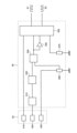
- FIG. 1 is a schematic diagram showing a configuration of an illumination device according to an embodiment of the present invention
- 1 is a schematic diagram showing a configuration of a light source of an illumination device according to an embodiment of the present invention
- 3 is a block diagram showing the configuration of a power supply device and a second control device of the lighting device according to one embodiment of the present invention
- FIG. 2 is a circuit diagram showing a partial circuit configuration of a control device for a lighting device according to an embodiment of the present invention.
- FIG. 4 is a schematic diagram illustrating a first pulse signal and a second pulse signal output from a second control device of the lighting device according to the embodiment of the present invention.
- drawings may show the width, thickness, shape, etc. of each part in a schematic manner compared to the actual embodiment, but these are merely examples, and the illustrated shapes themselves do not limit the interpretation of the present invention.
- elements with similar functions to those explained in relation to previous drawings in the specification may be given the same reference numerals, even if they are in different drawings, and duplicate explanations may be omitted.
- each structure When a film is processed to form multiple structures, each structure may have a different function or role, and each structure may be formed on a different base.
- these multiple structures originate from a film formed as the same layer in the same process, and are made of the same material. Therefore, these multiple films are defined as existing in the same layer.
- the term "above” is used, unless otherwise specified, to include both cases where another structure is placed directly above a structure, in contact with the structure, and cases where another structure is placed above a structure, with yet another structure in between.
- a lighting device 1 according to one embodiment of the present invention will be described. Note that, although the configuration of the lighting device 1 will be described below as one embodiment of the present invention, the embodiment of the present invention is not limited to the lighting device 1. A part of the configuration of the lighting device 1 may constitute an embodiment of the present invention.
- FIG. 1 is a schematic diagram showing the configuration of an illumination device 1 according to an embodiment of the present invention.
- the illumination device 1 includes an optical element 10, a light source 20, a first control device 30, a power supply device 40, and a second control device 50.
- the first control device 30 and the second control device 50 are control devices for the optical element 10 and the light source 20, respectively.
- the light emitted from the light source 20 passes through the optical element 10 and is emitted.
- the light source 20 is controlled by the second control device 50 to change the light emitted from the light source 20.
- the optical element 10 is controlled by the first control device 30 to change the light transmitted through the optical element 10.
- the second control device 50 controls the color adjustment or dimming
- the first control device 30 controls the light distribution.
- the optical element 10 includes four liquid crystal cells 100 stacked in the z-axis direction.
- the liquid crystal cell 100 has a configuration in which liquid crystal is sealed between two glass substrates on which transparent electrodes are formed in a comb-like shape.
- the first control device 30 generates a voltage signal to be applied to the transparent electrodes of the liquid crystal cells 100.
- FIG. 1 shows the optical element 10 including four liquid crystal cells 100, the number of liquid crystal cells 100 is not limited to four.
- the optical element 10 only needs to include at least two liquid crystal cells 100.
- the first control device 30 is connected to the four liquid crystal cells 100 of the optical element 10 and controls each liquid crystal cell 100 of the optical element 10. Specifically, the first control device 30 generates a voltage signal according to the light distribution.
- the first control device 30 is provided with eight volume knobs 31 that can be rotated by the user. By changing the combination of the rotation of the eight volume knobs 31 and the rotation angle of each of the eight volume knobs 31, the voltage signal applied to the transparent electrode of each liquid crystal cell 100 can be adjusted. In other words, the volume knobs 31 can adjust the light distribution of the light emitted from the optical element 10.
- FIG. 1 eight volume knobs 31 are shown, with two volume knobs 31 assigned to control one liquid crystal cell 100, but the number of volume knobs 31 is not limited to eight.
- the volume knobs 31 may be of a sliding type instead of a rotating type.
- the power supply device 40 is connected to the first control device 30 and the second control device 50, and generates a power supply voltage required to drive the first control device 30 and the second control device 50.
- the power supply device 40 may generate a plurality of power supply voltages.
- the power supply device 40 may also include a power supply voltage that is GND (e.g., 0 V). For convenience, this specification may be described as generating a power supply voltage even in the case of GND.
- FIG. 1 shows one power supply device 40
- the power supply device 40 may be divided into a power supply device that generates a power supply voltage to be supplied to the first control device 30 and a power supply device that generates a power supply voltage to be supplied to the second control device 50.
- the power supply device 40 may also be configured as an integrated unit with the first control device 30 or the second control device 50.
- the light source 20 is disposed above the optical element 10 and emits light to the optical element 10.
- the light source 20 for example, light emitting diodes (LEDs) can be used, but are not limited thereto.
- the light source 20 may be any element or device that can emit light.
- FIG. 2 is a schematic diagram showing the configuration of a light source 20 of a lighting device 1 according to one embodiment of the present invention.
- FIG. 2 shows a configuration using a light-emitting diode as an example of the light source 20.
- the light source 20 includes a base 21, a first light-emitting element 22, and a second light-emitting element 23.
- the first light-emitting element 22 and the second light-emitting element 23 are light-emitting diodes.
- a plurality of first light-emitting elements 22 and a plurality of second light-emitting elements 23 are arranged within the base 21.
- a first pulse signal generated by the second control device 50 is input to each of the plurality of first light-emitting elements 22.
- a second pulse signal generated by the second control device 50 is input to each of the plurality of second light-emitting elements 23.
- the color adjustment or dimming of the light source 20 can be controlled based on the first pulse signal and the second pulse signal. The first pulse signal and the second pulse signal will be described later.
- the multiple first light-emitting elements 22 and the multiple second light-emitting elements 23 are alternately arranged to form a circular shape.
- the arrangement of the multiple first light-emitting elements 22 and the multiple second light-emitting elements 23 is not limited to this. It is preferable that the multiple first light-emitting elements 22 and the multiple second light-emitting elements 23 are arranged symmetrically so that the light emitted from the light source 20 is uniformly incident on the optical element 10. It is preferable that the number of each of the first light-emitting elements 22 and the second light-emitting elements 23 is multiple, but this is not limited to this. The number of each of the first light-emitting elements 22 and the second light-emitting elements 23 may be one. Furthermore, the number of the first light-emitting elements 22 and the number of the second light-emitting elements 23 may be the same or different.
- the first light-emitting element 22 has a first light-emitting color.
- the second light-emitting element 23 has a second light-emitting color different from the first light-emitting color. For example, by combining the first light-emitting element 22 that emits blue light with the second light-emitting element 23 that emits yellow light, the light source 20 can emit white light.
- the first light-emitting element 22 having the first light-emitting color and the second light-emitting element 23 having the second light-emitting color may be combined so that light of incandescent color (color temperature 3000K), daylight color (color temperature 5000K), or daylight color (color temperature 6500K) is emitted from the light source 20.
- the second light-emitting element 23 may have a configuration in which a phosphor is provided in the first light-emitting element 22 and the first light-emitting color is converted to the second light-emitting color by the phosphor.
- the light source 20 can be configured in a manner other than white light, and the first light-emitting color and the second light-emitting color are not particularly limited.
- a reflector may be provided on the inner side of the base 21.
- the light emitted from the first light-emitting element 22 and the second light-emitting element 23 is reflected by the reflector and emitted from the light source 20. This increases the amount of light incident on the optical element 10.
- the second control device 50 is connected to the light source 20 and controls the first light-emitting element 22 and the second light-emitting element 23 of the light source 20. Specifically, the second control device 50 generates a first pulse signal input to the first light-emitting element 22 and a second pulse signal input to the second light-emitting element 23 according to color adjustment or dimming.
- the second control device 50 is provided with a first volume knob 51 and a second volume knob 52 that can be rotated by the user. By adjusting the rotation angle of the first volume knob 51, the color adjustment of the light source 20 can be controlled. In addition, by adjusting the rotation angle of the second volume knob 52, the dimming of the light source 20 can be controlled. Note that the first volume knob 51 and the second volume knob 52 may be of a sliding type instead of a rotating type.
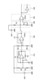
- FIG. 3 is a block diagram showing the configuration of the power supply device 40 and the second control device 50 of the lighting device 1 according to one embodiment of the present invention.
- the power supply device 40 includes a first power supply 410, a second power supply 420, and a third power supply 430.
- the second control device 50 also includes an oscillator circuit 510, an integrator circuit 520, a comparator circuit 530, an inverter 540, a driver circuit 550, a first variable resistor 560, and a second variable resistor 570.
- the first volume knob 51 is connected to the first variable resistor 560, and when the user rotates the first volume knob 51, the resistance of the first variable resistor 560 changes.
- the second volume knob 52 is connected to the second variable resistor 570, and when the user rotates the second volume knob 52, the resistance of the second variable resistor 570 changes.
- the first power supply 410 is electrically connected to the drive circuit 550 and supplies a power supply voltage for driving the drive circuit 550.
- the second power supply 420 is electrically connected to the oscillation circuit 510 and supplies a power supply voltage for the oscillation circuit 510 to generate a pulse voltage.
- the third power supply 430 is electrically connected to the first variable resistor 560 and supplies a power supply voltage for generating a threshold voltage that is input to the comparison circuit 530.
- the oscillator circuit 510 generates and outputs a first pulse voltage.
- the oscillator circuit 510 is electrically connected to the integrator circuit 520, and the first pulse voltage output from the oscillator circuit 510 is input to the integrator circuit 520.
- the integration circuit 520 converts the first pulse voltage into a triangular wave voltage and outputs it.
- the integration circuit 520 is electrically connected to the comparison circuit 530, and the triangular wave voltage output from the integration circuit 520 is input to the comparison circuit 530.
- the comparison circuit 530 is connected to the integration circuit 520 and the first variable resistor 560.
- the comparison circuit 530 receives the triangular wave voltage from the integration circuit 520 and the threshold voltage from the first variable resistor 560.
- the comparison circuit 530 compares the triangular wave voltage with the threshold voltage to generate a second pulse voltage.
- the comparison circuit 530 generates a second pulse voltage that is turned on when the triangular wave voltage is equal to or greater than the threshold voltage and turned off when the triangular wave voltage is less than the threshold voltage.
- the threshold voltage varies depending on the resistance of the first variable resistor 560. Therefore, the on period of the second pulse voltage can be controlled by adjusting the resistance of the first variable resistor 560. That is, the second pulse voltage is a PWM (Pulse Width Modulation) voltage in which the on period and the off period are controlled.
- the duty ratio of the on-period of the second pulse voltage is determined by the threshold voltage.
- the comparison circuit 530 outputs the second pulse voltage and a third pulse voltage in which the phase of the second pulse voltage is inverted by the inverter 540.
- the on-period of the third pulse voltage corresponds to the off-period of the second pulse voltage.
- the comparison circuit 530 and the inverter 540 are electrically connected to the drive circuit 550, and the second pulse voltage and the third pulse voltage are input to the drive circuit 550.
- the driving circuit 550 is electrically connected to the comparison circuit 530, the inverter 540, and the second variable resistor 570.
- the driving circuit 550 converts the second pulse voltage and the third pulse voltage into a first pulse signal S1 that drives the first light-emitting element 22 and a second pulse signal S2 that drives the second light-emitting element 23, respectively.
- the first pulse signal S1 and the second pulse signal S2 are generated based on the second pulse voltage and the third pulse voltage, respectively, and at this time, the amplitudes of the first pulse signal S1 and the second pulse signal S2 change depending on the resistance of the second variable resistor 570. That is, by adjusting the resistance of the second variable resistor 570, the amplitudes of the first pulse signal S1 and the second pulse signal S2 can be controlled.
- the first light-emitting element 22 to which the first pulse signal S1 is input can emit light only during the on-period corresponding to the duty ratio.
- the same is true for the second light-emitting element 23 to which the second pulse signal S2 is input. That is, the light source 20 including the first light-emitting element 22 and the second light-emitting element 23 is controlled by PWM drive.
- the duty ratio is changed, the light emission period of the first light-emitting element 22 with the first light-emitting color and the light emission period of the second light-emitting element 23 with the second light-emitting element 23 change, and the color of the light emitted from the light source 20 changes.
- the second control device 50 can generate the first pulse signal S1 and the second pulse signal S2 that control the color adjustment and dimming of the light source 20.
- the circuit configuration of the second control circuit 500 will be described with reference to FIG. 4, but below, the oscillator circuit 510, the integrator circuit 520, and the comparator circuit 530 will be mainly described.
- the second control circuit 500 a circuit configuration using an operational amplifier is applied, so expensive components such as a microcomputer or a DAC are not required. Therefore, the manufacturing cost of the lighting device 1 can be reduced.
- FIG. 4 is a circuit diagram showing a part of the circuit configuration of the second control circuit 50 of the lighting device 1 according to one embodiment of the present invention. Note that FIG. 4 is an example of the circuit configuration of the second control circuit 500, and the circuit configuration of the second control circuit 500 is not limited to this. Also, FIG. 4 omits power supply connections and the like that would be understandable to a person skilled in the art.
- the oscillator circuit 510 includes a first operational amplifier OPA1.
- the inverting input terminal (-) is connected to the output terminal via a resistive element R1.
- the inverting input terminal (-) is also connected to a capacitive element C1.
- the non-inverting input terminal (+) is connected to the output terminal via a resistive element R2.
- the non-inverting input terminal (+) is also connected to the second power supply 420 via a resistive element R3, and is connected to GND via a resistive element R4.
- the resistive elements R1 and R2 function as feedback resistors.
- the resistive elements R3 and R4 function as voltage division resistors.
- the integrating circuit 520 includes a second operational amplifier OPA2.
- the inverting input terminal (-) is connected to the output terminal via a capacitance element C2.
- the inverting input terminal (-) is also connected to the output terminal of the first operational amplifier OPA1, and a first pulse voltage is input to the inverting input terminal (-).
- the non-inverting input terminal (+) is connected to the second power supply 420 via a resistance element R5, and is connected to GND via a resistance element R6.
- the capacitance element C2 functions as a feedback resistor.
- the resistance elements R5 and R6 function as voltage dividing resistors.
- the comparison circuit 530 includes a third operational amplifier OPA3.
- the inverting input terminal (-) is connected to the output terminal of the second operational amplifier OPA2, and a triangular wave voltage is input to the inverting input terminal (-).
- the non-inverting input terminal (+) is connected to the first variable resistor 560.
- the first variable resistor 560 is connected to the third power supply 430. Therefore, a threshold voltage according to the resistance of the first variable resistor 560 is input to the non-inverting input terminal (+).
- the triangular wave voltage input to the inverting input terminal (-) is compared with the threshold voltage input to the non-inverting input terminal (+).
- a HIGH voltage is output from the output terminal. If the triangular wave voltage is less than the threshold voltage, a LOW voltage is output from the output terminal. That is, a second pulse voltage in which a HIGH voltage and a LOW voltage are repeated is output from the output terminal of the third operational amplifier OPA3.
- the period of the HIGH voltage is determined by the threshold voltage. Specifically, as the threshold voltage increases, the period of the HIGH voltage becomes shorter, and as the threshold voltage decreases, the period of the HIGH voltage becomes longer. Therefore, the second pulse voltage is a PWM voltage whose duty ratio can be adjusted by the threshold voltage.
- the first variable resistor 560 includes, for example, a resistive element R7 and a variable resistive element Rv.
- the resistive element R7 is connected in series with the variable resistive element Rv.
- the resistive element R7 functions as a fixed resistor that determines the range of the threshold voltage output via the first variable resistor 560. For example, even if the power supply voltage generated by the third power supply 430 is +15V, by connecting the resistive element R7 to the variable resistive element Rv, the range of the threshold voltage output via the variable resistive element Rv (such as 0 to +10V) can be adjusted.
- the second pulse voltage output from the output terminal of the third operational amplifier OPA3 of the comparison circuit 530 has its phase inverted by the inverter 540.
- the comparison circuit 530 and the inverter 540 are connected to the drive circuit 550.
- the second pulse voltage and a third pulse voltage in which the phase of the second pulse voltage is inverted are input to the drive circuit 550.
- the period of the HIGH voltage in the third pulse voltage corresponds to the period of the LOW voltage in the second pulse voltage. Therefore, the third pulse voltage is also a PWM voltage whose duty ratio is adjusted by the threshold voltage.
- FIG. 5 is a schematic diagram illustrating the first pulse signal S1 and the second pulse signal S2 output from the second control device 50 of the lighting device according to one embodiment of the present invention. Specifically, FIG. 5 shows the second pulse voltage P2 (duty ratio p%) and the third pulse voltage P3 (duty ratio q%) whose duty ratios are adjusted and input to the drive circuit 550, as well as the first pulse signal S1 and the second pulse signal S2 output from the drive circuit 550.
- the second pulse voltage P2 and the third pulse voltage P3 are converted into signals for driving the first light-emitting element 22 and the second light-emitting element 23, respectively.
- the first pulse signal S1 for driving the first light-emitting element 22 is generated based on the second pulse voltage P2. Therefore, the first pulse signal S1 has the same duty ratio p% as the second pulse voltage P2.
- the second pulse signal S2 for driving the second light-emitting element 23 is generated based on the third pulse voltage P3. Therefore, the second pulse signal S2 has the same duty ratio q% as the third pulse voltage P3.
- the light source 20 including the first light-emitting element 22 and the second light-emitting element 23 is controlled by PWM drive.
- the first light-emitting element 22 is driven to emit light having a first emission color.
- the second light-emitting element 23 is driven to emit light having a second emission color.
- a second variable resistor 570 is electrically connected to the drive circuit 550.
- the amplitude of each of the first pulse signal S1 and the second pulse signal S2 changes depending on the resistance of the second variable resistor 570.
- the amplitude of the first pulse signal S1 increases, the luminance of the first light-emitting element 22 to which the first pulse is input increases.
- the second light-emitting element 23 to which the second pulse signal S2 is input Therefore, in the lighting device 1, the luminance of the light emitted from the light source 20 can be changed by adjusting the resistance of the second variable resistor 570.
- the color tuning of the light source 20 can be controlled by adjusting the resistance of the first variable resistor 560 of the second control device 50, and the dimming of the light source 20 can be controlled by adjusting the resistance of the second variable resistor 570 of the second control device 50.
- the lighting device 1 can control the color or dimming of the light source 20 without using expensive components such as a microcomputer and a DAC. Therefore, the lighting device 1 can reduce manufacturing costs.
Landscapes
- Circuit Arrangement For Electric Light Sources In General (AREA)
Priority Applications (3)
| Application Number | Priority Date | Filing Date | Title |
|---|---|---|---|
| JP2024574304A JPWO2024161808A1 (https=) | 2023-01-31 | 2023-12-12 | |
| CN202380085337.4A CN120283445A (zh) | 2023-01-31 | 2023-12-12 | 控制装置及照明装置 |
| US19/264,396 US20250344302A1 (en) | 2023-01-31 | 2025-07-09 | Control device and illumination device |
Applications Claiming Priority (2)
| Application Number | Priority Date | Filing Date | Title |
|---|---|---|---|
| JP2023-013322 | 2023-01-31 | ||
| JP2023013322 | 2023-01-31 |
Related Child Applications (1)
| Application Number | Title | Priority Date | Filing Date |
|---|---|---|---|
| US19/264,396 Continuation US20250344302A1 (en) | 2023-01-31 | 2025-07-09 | Control device and illumination device |
Publications (1)
| Publication Number | Publication Date |
|---|---|
| WO2024161808A1 true WO2024161808A1 (ja) | 2024-08-08 |
Family
ID=92146347
Family Applications (1)
| Application Number | Title | Priority Date | Filing Date |
|---|---|---|---|
| PCT/JP2023/044405 Ceased WO2024161808A1 (ja) | 2023-01-31 | 2023-12-12 | 制御装置および照明装置 |
Country Status (4)
| Country | Link |
|---|---|
| US (1) | US20250344302A1 (https=) |
| JP (1) | JPWO2024161808A1 (https=) |
| CN (1) | CN120283445A (https=) |
| WO (1) | WO2024161808A1 (https=) |
Citations (3)
| Publication number | Priority date | Publication date | Assignee | Title |
|---|---|---|---|---|
| JP2008070592A (ja) * | 2006-09-12 | 2008-03-27 | Samsung Electronics Co Ltd | 輝度調整装置及び液晶表示装置 |
| JP2012146614A (ja) * | 2010-01-29 | 2012-08-02 | Mitsubishi Chemicals Corp | 白色led発光デバイスの調光装置,及び照明システム |
| WO2022270298A1 (ja) * | 2021-06-23 | 2022-12-29 | 株式会社ジャパンディスプレイ | 光学装置 |
-
2023
- 2023-12-12 JP JP2024574304A patent/JPWO2024161808A1/ja active Pending
- 2023-12-12 WO PCT/JP2023/044405 patent/WO2024161808A1/ja not_active Ceased
- 2023-12-12 CN CN202380085337.4A patent/CN120283445A/zh active Pending
-
2025
- 2025-07-09 US US19/264,396 patent/US20250344302A1/en active Pending
Patent Citations (3)
| Publication number | Priority date | Publication date | Assignee | Title |
|---|---|---|---|---|
| JP2008070592A (ja) * | 2006-09-12 | 2008-03-27 | Samsung Electronics Co Ltd | 輝度調整装置及び液晶表示装置 |
| JP2012146614A (ja) * | 2010-01-29 | 2012-08-02 | Mitsubishi Chemicals Corp | 白色led発光デバイスの調光装置,及び照明システム |
| WO2022270298A1 (ja) * | 2021-06-23 | 2022-12-29 | 株式会社ジャパンディスプレイ | 光学装置 |
Also Published As
| Publication number | Publication date |
|---|---|
| CN120283445A (zh) | 2025-07-08 |
| JPWO2024161808A1 (https=) | 2024-08-08 |
| US20250344302A1 (en) | 2025-11-06 |
Similar Documents
| Publication | Publication Date | Title |
|---|---|---|
| US11419194B2 (en) | LED light apparatus | |
| EP1782660B1 (en) | Method and apparatus for scaling the average current supply to light-emitting elements | |
| KR20090051236A (ko) | Pwm 방법 및 장치, 및 그에 의해 구동되는 광원 | |
| KR101153219B1 (ko) | 디밍 신호를 이용한 dc-dc 컨버터용 pwm 신호 발생회로 및 방법과 이를 구비한 백라이트용 led 구동 회로 | |
| JP5303121B2 (ja) | Led照明装置およびその駆動方法 | |
| US20050062440A1 (en) | Systems and methods for controlling illumination sources | |
| KR100902548B1 (ko) | 엘이디 백라이트 유닛 및 이를 포함하는 디스플레이 장치 | |
| JPH01137599A (ja) | 輝度調整蛍光照明装置、蛍光ランプ調光装置及び方法 | |
| US9380668B2 (en) | PDM modulation of LED current | |
| CN101527988A (zh) | 光源驱动模块及电路 | |
| KR101029546B1 (ko) | 색온도 제어가 가능한 발광장치 | |
| US20240023215A1 (en) | Multi-function lighting device | |
| WO2024161808A1 (ja) | 制御装置および照明装置 | |
| US11792900B2 (en) | High resolution dimmer circuit | |
| CN118075946A (zh) | 用于实现调光的照明控制器 | |
| CN101236725A (zh) | 发光模块的驱动装置及其驱动方法 | |
| KR20230090813A (ko) | 두 개의 전원 배선을 이용한 조색조광 기능을 갖는 led 조명 장치 | |
| US12464612B2 (en) | Controller for bathtub lamp | |
| CN222030097U (zh) | 照明控制器以及照明电路 | |
| CN114974145B (zh) | Led驱动电路及方法 | |
| TWI734324B (zh) | 光源調整系統 | |
| WO2025249065A1 (ja) | 照明装置 | |
| KR101034705B1 (ko) | 백라이트 어셈블리 및 그 구동방법 | |
| JPH0438382Y2 (https=) | ||
| KR20200046760A (ko) | 발광 소자 구동 장치 |
Legal Events
| Date | Code | Title | Description |
|---|---|---|---|
| 121 | Ep: the epo has been informed by wipo that ep was designated in this application |
Ref document number: 23919943 Country of ref document: EP Kind code of ref document: A1 |
|
| WWE | Wipo information: entry into national phase |
Ref document number: 2024574304 Country of ref document: JP |
|
| WWE | Wipo information: entry into national phase |
Ref document number: 202380085337.4 Country of ref document: CN |
|
| WWP | Wipo information: published in national office |
Ref document number: 202380085337.4 Country of ref document: CN |
|
| NENP | Non-entry into the national phase |
Ref country code: DE |
|
| 122 | Ep: pct application non-entry in european phase |
Ref document number: 23919943 Country of ref document: EP Kind code of ref document: A1 |