WO2024161683A1 - 積層型コイルおよび積層型コイルアレイ - Google Patents
積層型コイルおよび積層型コイルアレイ Download PDFInfo
- Publication number
- WO2024161683A1 WO2024161683A1 PCT/JP2023/030019 JP2023030019W WO2024161683A1 WO 2024161683 A1 WO2024161683 A1 WO 2024161683A1 JP 2023030019 W JP2023030019 W JP 2023030019W WO 2024161683 A1 WO2024161683 A1 WO 2024161683A1
- Authority
- WO
- WIPO (PCT)
- Prior art keywords
- coil
- external electrode
- conductor
- element body
- lead conductor
- Prior art date
- Legal status (The legal status is an assumption and is not a legal conclusion. Google has not performed a legal analysis and makes no representation as to the accuracy of the status listed.)
- Ceased
Links
Images




Classifications
-
- H—ELECTRICITY
- H01—ELECTRIC ELEMENTS
- H01F—MAGNETS; INDUCTANCES; TRANSFORMERS; SELECTION OF MATERIALS FOR THEIR MAGNETIC PROPERTIES
- H01F27/00—Details of transformers or inductances, in general
- H01F27/28—Coils; Windings; Conductive connections
- H01F27/32—Insulating of coils, windings, or parts thereof
- H01F27/324—Insulation between coil and core, between different winding sections, around the coil; Other insulation structures
-
- H—ELECTRICITY
- H01—ELECTRIC ELEMENTS
- H01F—MAGNETS; INDUCTANCES; TRANSFORMERS; SELECTION OF MATERIALS FOR THEIR MAGNETIC PROPERTIES
- H01F17/00—Fixed inductances of the signal type
-
- H—ELECTRICITY
- H01—ELECTRIC ELEMENTS
- H01F—MAGNETS; INDUCTANCES; TRANSFORMERS; SELECTION OF MATERIALS FOR THEIR MAGNETIC PROPERTIES
- H01F17/00—Fixed inductances of the signal type
- H01F17/0006—Printed inductances
- H01F17/0013—Printed inductances with stacked layers
-
- H—ELECTRICITY
- H01—ELECTRIC ELEMENTS
- H01F—MAGNETS; INDUCTANCES; TRANSFORMERS; SELECTION OF MATERIALS FOR THEIR MAGNETIC PROPERTIES
- H01F17/00—Fixed inductances of the signal type
- H01F17/04—Fixed inductances of the signal type with magnetic core
-
- H—ELECTRICITY
- H01—ELECTRIC ELEMENTS
- H01F—MAGNETS; INDUCTANCES; TRANSFORMERS; SELECTION OF MATERIALS FOR THEIR MAGNETIC PROPERTIES
- H01F27/00—Details of transformers or inductances, in general
- H01F27/28—Coils; Windings; Conductive connections
- H01F27/29—Terminals; Tapping arrangements for signal inductances
-
- H—ELECTRICITY
- H01—ELECTRIC ELEMENTS
- H01F—MAGNETS; INDUCTANCES; TRANSFORMERS; SELECTION OF MATERIALS FOR THEIR MAGNETIC PROPERTIES
- H01F27/00—Details of transformers or inductances, in general
- H01F27/28—Coils; Windings; Conductive connections
- H01F27/29—Terminals; Tapping arrangements for signal inductances
- H01F27/292—Surface mounted devices
-
- H—ELECTRICITY
- H01—ELECTRIC ELEMENTS
- H01F—MAGNETS; INDUCTANCES; TRANSFORMERS; SELECTION OF MATERIALS FOR THEIR MAGNETIC PROPERTIES
- H01F37/00—Fixed inductances not covered by group H01F17/00
Definitions
- This disclosure relates to stacked coils and stacked coil arrays.
- Patent Document 1 which shows an example of the above-mentioned inductor, describes a stacked coil array for a DC-DC converter, comprising an element body including a magnetic layer containing magnetic particles, a first coil and a second coil built into the element body, and a first external electrode, a second external electrode, a third external electrode and a fourth external electrode provided on the surface of the element body and electrically connected to one of the ends of the first coil and the second coil, respectively, wherein a non-magnetic layer is provided between the first coil and the second coil, and each of the first coil and the second coil is formed by connecting a plurality of coil conductors in the stacking direction, and the above of the first coil is described.
- a stacked coil array for a DC-DC converter in which an end drawn from the coil conductor closest to the second coil among the multiple coil conductors is connected to the first external electrode, and the other end of the first coil is connected to the second external electrode, an end drawn from the coil conductor closest to the first coil among the multiple coil conductors of the second coil is connected to the third external electrode, and the other end of the second coil is connected to the fourth external electrode, and the first external electrode and the third external electrode are connected to output terminals of switching elements of a DC-DC converter.
- the primary objective of this disclosure is to provide a stacked coil and a stacked coil array that reduce degradation of electrical characteristics.
- the laminated coil of the present disclosure is an element body having magnetic layers laminated thereon; a first coil provided inside the element body and including a plurality of first coil conductor layers in a stacking direction; and a second coil including a plurality of second coil conductor layers in the stacking direction; a first external electrode and a second external electrode electrically connected to the first coil; a third external electrode and a fourth external electrode electrically connected to the second coil, the first to fourth external electrodes are disposed on a bottom surface of the element body, the second coil is provided at a position farther from a bottom surface of the element body than the first coil in the stacking direction, a first lead conductor provided inside the element body and connecting an end of the first coil conductor layer that is closest to the bottom surface among the ends of the first coil and the first external electrode; a second lead conductor provided inside the element body and connecting the other end of the first coil and the second external electrode; a third lead conductor provided inside the element body and connecting an end of the second coil conductor layer that is closest to the bottom surface
- the stacked coil array of the present disclosure is an element body having magnetic layers laminated thereon; a first coil provided inside the element body, the first coil including a plurality of first coil conductor layers in a stacking direction, a second coil including a plurality of second coil conductor layers in the stacking direction, a third coil including a plurality of third coil conductor layers in the stacking direction, and a fourth coil including a plurality of fourth coil conductor layers in the stacking direction; a first external electrode and a second external electrode electrically connected to the first coil; a third external electrode and a fourth external electrode electrically connected to the second coil; a fifth external electrode and a sixth external electrode electrically connected to the third coil; a seventh external electrode and an eighth external electrode electrically connected to the fourth coil, the first to eighth external electrodes are disposed on a bottom surface of the element body, the second coil is provided at a position farther from a bottom surface of the element body than the first coil in the stacking direction, the fourth coil is provided at a position farther from
- the present disclosure it is possible to provide a stacked coil and a stacked coil array that reduce the degradation of electrical characteristics. Specifically, because the second external electrode and the third external electrode are directly connected, even if an unexpected voltage occurs in the stacked coil or the like, it is possible to prevent the coils in the element from shorting out with each other, and reduce the occurrence of a decrease in the insulation resistance between the coils. Therefore, it is possible to reduce the degradation of the electrical characteristics of the stacked coil or the like.
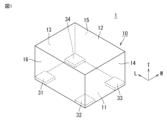
- FIG. 1 is a perspective view illustrating an example of a multilayer coil according to a first embodiment.
- FIG. 2 is a perspective view illustrating an example of the internal structure of the laminated coil according to the first embodiment.
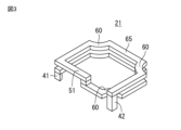
- FIG. 3 is a perspective view of the internal structure shown in FIG. 2 , showing the first coil, the first lead conductor, and the second lead conductor.
- FIG. 4 is a perspective view of the internal structure shown in FIG. 2, in which the second coil, the third lead conductor, and the fourth lead conductor are extracted.
- FIG. 5 is an exploded perspective view of the internal structure shown in FIG.
- FIG. 6 is a cross-sectional view taken along line VI-VI of FIG.
- FIG. 7 is a perspective view illustrating an example of an internal structure of a modified example of the first embodiment.
- FIG. 1 is a perspective view illustrating an example of a multilayer coil according to a first embodiment.
- FIG. 2 is a perspective view illustrating an example of the internal structure of the laminated coil according to
- FIG. 8A is a perspective view (top view) that illustrates an example of the internal structure of the laminated coil according to the second embodiment.
- FIG. 8B is a perspective view (as viewed from the bottom) that illustrates an example of the internal structure of the laminated coil according to the second embodiment.
- FIG. 9 is an exploded perspective view of a portion of the internal structure of the laminated coil according to the second embodiment.
- FIG. 10 is a perspective view (top view) illustrating a schematic example of an internal structure of the laminated coil according to the third embodiment.
- FIG. 11 is an exploded perspective view of a portion of the internal structure of the laminated coil according to the third embodiment.
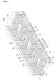
- FIG. 12A is a perspective view showing a schematic example of the internal structure of a stacked coil array according to the present disclosure.
- FIG. 12B is a perspective view that illustrates an example of the internal structure of the stacked coil array of the present disclosure.
- FIG. 12C is a perspective view that illustrates an example of the internal structure of the
- stacked coil and stacked coil array of the present disclosure are described below. Note that the present disclosure is not limited to the configurations below, and may be modified as appropriate without departing from the gist of the present disclosure. In addition, combinations of multiple individual preferred configurations described below also constitute the present disclosure.
- the stacked coil and stacked coil array of the present disclosure are used, for example, in DC-DC converters.
- the stacked coil and stacked coil array of the present disclosure can also be used for purposes other than DC-DC converters.
- Figure 1 is a perspective view showing an example of the laminated coil according to the first embodiment
- Figure 2 is a perspective view showing an example of the internal structure of the laminated coil according to the first embodiment
- Figure 3 is a perspective view showing the first coil, the first lead conductor, and the second lead conductor extracted from the internal structure shown in Figure 2
- Figure 4 is a perspective view showing the second coil, the third lead conductor, and the fourth lead conductor extracted from the internal structure shown in Figure 2
- Figure 5 is an exploded perspective view of the internal structure shown in Figure 2
- Figure 6 is a cross-sectional view taken along the arrows IV-IV in Figure 5.
- the shapes and arrangements of the laminated coil and the components are not limited to those shown in the figures.
- the laminated coil 1 shown in Figures 1 and 2 comprises a base body 10, a first coil 21, a second coil 22, a first external electrode 31, a second external electrode 32, a third external electrode 33, a fourth external electrode 34, a first lead conductor 41, a second lead conductor 42, a third lead conductor 43, and a fourth lead conductor 44.
- a base body 10 a first coil 21, a second coil 22, a first external electrode 31, a second external electrode 32, a third external electrode 33, a fourth external electrode 34, a first lead conductor 41, a second lead conductor 42, a third lead conductor 43, and a fourth lead conductor 44.
- the element body 10 has, for example, a rectangular parallelepiped shape or a substantially rectangular parallelepiped shape having six sides.
- the corners and ridges of the element body 10 may be rounded.
- a corner is a portion where three sides of the element body 10 intersect, and a ridge is a portion where two sides of the element body 10 intersect.
- the length, width, and height directions of the stacked coil 1 and the base body 10 are shown as L, W, and T directions, respectively.
- the length direction L, width direction W, and height direction T are mutually orthogonal.
- the mounting surface of the stacked coil 1 is, for example, a surface (LW surface) parallel to the length direction L and width direction W.
- the base body 10 shown in FIG. 1 has a first main surface 11 and a second main surface 12 that face the height direction T, a first end surface 13 and a second end surface 14 that face the length direction L perpendicular to the height direction T, and a first side surface 15 and a second side surface 16 that face the width direction W perpendicular to the length direction L and the height direction T.
- the first main surface 11 of the base body 10 corresponds to the bottom surface of the base body 10.
- the base body 10 includes a magnetic layer S (see FIG. 5). It is preferable that the base body 10 has a laminated structure. Specifically, it is preferable that the base body 10 includes multiple magnetic layers S in a lamination direction (e.g., height direction T). In this embodiment, as shown in FIG. 5, the base body 10 may be constructed by laminating magnetic layer groups G1 to G11, each including at least one magnetic layer S. It is not necessary for the boundaries between the layers of the laminated structure of the base body 10 to be clearly visible.
- the magnetic layer group G1 has, as an example, two magnetic layers S, and constitutes the second main surface 12 of the base body 10.
- the magnetic layer group G2 has, as an example, four magnetic layers S. Second coil conductor layers 52 are provided on the magnetic layers S, and these four second coil conductor layers 52 form one winding of the second coil 22.
- the magnetic layer group G3 has one magnetic layer S.
- the magnetic layer S is provided with a conductor layer (via conductor) for connecting the second coil conductor layer 52 of the magnetic layer group G2 to the second coil conductor layer 52 of the magnetic layer group G4, and a fourth lead conductor 44 for electrically connecting the second coil conductor layer 52 to the fourth external electrode 34.
- the magnetic layer group G4 has, as an example, four magnetic layers S. Second coil conductor layers 52 are provided on the magnetic layers S, and these four second coil conductor layers 52 form another winding of the second coil 22. In addition, a fourth lead conductor 44 is provided at a corner of the magnetic layer group G4.
- the magnetic layer group G5 has, as an example, two magnetic layers S.
- the magnetic layer S is provided with a third lead conductor 43 for electrically connecting the second coil conductor layer 52 and the third external electrode 33, and a fourth lead conductor 44 for electrically connecting the second coil conductor layer 52 and the fourth external electrode 34.
- the magnetic layer group G6 has, as an example, four magnetic layers S.
- the magnetic layers S are provided with first coil conductor layers 51, and these four first coil conductor layers 51 form one winding of the first coil 21.
- the above-mentioned fourth lead conductor 44 and third lead conductor 43 are provided at one corner of each magnetic layer S.
- the magnetic layer group G7 has one magnetic layer S, as an example.
- the magnetic layer S is provided with a conductor layer (via conductor) for connecting the first coil conductor layer 51 of the magnetic layer group G6 to the first coil conductor layer 51 of the magnetic layer group G8, and a second lead conductor 42 for electrically connecting the first coil conductor layer 51 to the second external electrode 32.
- the magnetic layer group G7 has the above-mentioned fourth lead conductor 44 and third lead conductor 43 provided at one corner of each magnetic layer S.
- the magnetic layer group G8 has, as an example, four magnetic layers S.
- the magnetic layers S are provided with first coil conductor layers 51, and these four first coil conductor layers 51 form the other windings of the first coil 21.
- the above-mentioned fourth lead conductor 44 and third lead conductor 43 are provided at the corners on one side of each magnetic layer S.
- a second lead conductor 42 is provided at the corners on the other side of each magnetic layer S.
- the magnetic layer group G9 has, as an example, two magnetic layers S.
- the magnetic layer S has a first lead conductor 41, a second lead conductor 42, a third lead conductor 43, and a fourth lead conductor 44 at the corners.
- the magnetic layer group G10 has, as an example, two magnetic layers S.
- the magnetic layer S is provided with a first lead conductor 41, a fourth lead conductor 44, and a conductor wiring H1 for directly connecting the second external electrode 32 and the third external electrode 33.
- the magnetic layer group G11 has, as an example, two magnetic layers S.
- the magnetic layer S is provided with a first external electrode 31, a second external electrode 32, a third external electrode 33, and a fourth external electrode 34.
- the degree of freedom in designing the laminated coil 1 is increased.
- the degree of freedom in designing the laminated coil 1 is increased.
- a laminated coil 1 having a first external electrode 31, a second external electrode 32, a third external electrode 33, and a fourth external electrode 34 on the bottom surface (first main surface 11) of the element body 10 it becomes easier to pull out the first coil 21 and the second coil 22 to the bottom surface side.
- the magnetic layer S includes magnetic particles made of a magnetic material.
- the magnetic particles may be particles of a metal magnetic material (metal magnetic particles) such as Fe, Co, Ni, and alloys containing at least one of these, or ferrite particles.
- the magnetic particles are preferably Fe particles or Fe alloy particles.
- As the Fe alloy Fe-Si alloys, Fe-Si-Cr alloys, Fe-Si-Al alloys, Fe-Si-B-P-Cu-C alloys, Fe-Si-B-Nb-Cu alloys, etc. are preferred.
- the surfaces of the metal magnetic particles made of the above-mentioned metal magnetic material are preferably covered with an insulating coating.
- an insulating coating When the surfaces of the metal magnetic particles are covered with an insulating coating, the insulation between the metal magnetic particles can be improved.
- Methods for forming the insulating coating on the surfaces of the metal magnetic particles include the sol-gel method and the mechanochemical method.
- the material constituting the insulating coating is preferably an oxide of P, Si, or the like.
- the insulating coating may also be an oxide film formed by oxidizing the surfaces of the metal magnetic particles.
- the thickness of the insulating coating is preferably 1 nm or more and 50 nm or less, more preferably 1 nm or more and 30 nm or less, and even more preferably 1 nm or more and 20 nm or less.
- SEM scanning electron microscope
- the average particle size of the metal magnetic particles in the magnetic layer S is preferably 1 ⁇ m or more and 30 ⁇ m or less, more preferably 1 ⁇ m or more and 20 ⁇ m or less, and even more preferably 1 ⁇ m or more and 10 ⁇ m or less.
- the average particle size of the metal magnetic particles in the magnetic layer can be measured by the procedure described below.
- a cross section of a laminated coil sample is cut, and multiple (e.g., 5) areas (e.g., 130 ⁇ m x 100 ⁇ m) are photographed with an SEM, and the obtained SEM images are analyzed using image analysis software (e.g., image analysis software WinROOF2021 (manufactured by Mitani Shoji Co., Ltd.)) to determine the circular equivalent diameter of the metal magnetic particles.
- image analysis software e.g., image analysis software WinROOF2021 (manufactured by Mitani Shoji Co., Ltd.)
- the average value of the obtained circular equivalent diameters is regarded as the average particle size of the metal magnetic particles.
- the metal magnetic particles contained in the element body 10 have an oxide film on the surface. This oxide film originates from the metal magnetic particles and is formed by the heat treatment. In the element body 10, adjacent metal magnetic particles are bonded to each other via the oxide film.
- the base body 10 may include a non-magnetic layer between the first coil 21 and the second coil 22.
- a non-magnetic layer between the first coil 21 and the second coil 22 By providing a non-magnetic layer between the first coil 21 and the second coil 22, the insulation between the first coil 21 and the second coil 22 can be improved, and a short circuit between the two can be prevented.
- the non-magnetic layer may contain a glass ceramic material and a non-magnetic ferrite material as the non-magnetic material.
- the non-magnetic layer preferably contains a non-magnetic ferrite material as the non-magnetic material.
- a non-magnetic ferrite material having a composition in which Fe is 40 mol% or more and 49.5 mol% or less when calculated as Fe 2 O 3 , Cu is 6 mol% or more and 12 mol% or less when calculated as CuO, and the remainder is ZnO can be used.
- the non-magnetic material may contain Mn 3 O 4 , Co 3 O 4 , SnO 2 , Bi 2 O 3 , SiO 2, etc. as additives as necessary, and may contain a small amount of inevitable impurities.
- the non-magnetic layer preferably contains Zn-Cu ferrite.
- the thickness of the non-magnetic layer can be measured using the procedure described below.
- a stacked coil sample is set vertically and the sample is hardened with resin so that the LT surface is exposed.
- the sample is polished to a depth of approximately 1/2 in the W direction using a polishing machine, exposing a cross section parallel to the LT surface.
- the polished surface is processed by ion milling (Ion Milling Machine IM4000, manufactured by Hitachi High-Tech Corporation) to remove any sagging of the internal conductor caused by polishing.
- the approximate center of the non-magnetic layer in the polished sample is photographed with an SEM, and the thickness of the approximate center of the non-magnetic layer is measured from the obtained SEM photograph, and this is defined as the thickness of the non-magnetic layer.
- the base body 10 may include a non-magnetic portion between the multiple first coil conductor layers 51 that constitute the first coil 21, or between the multiple second coil conductor layers 52 that constitute the second coil 22.
- the non-magnetic portion is provided in at least one location between adjacent coil conductor layers of the first coil conductor layer 51 and the second coil conductor layer 52.
- the nonmagnetic layer and the nonmagnetic portion preferably have the same composition.
- the nonmagnetic layer and the nonmagnetic portion preferably are composed of Zn-Cu ferrite.
- a first coil 21 and a second coil 22 are provided inside the base body 10. It is preferable that the first coil 21 and the second coil 22 are magnetically coupled. Furthermore, one end of the first coil 21 and one end of the second coil 22 may be electrically connected as described below. Note that, two coils including only the first coil 21 and the second coil 22 may be provided inside the base body 10, or three or more coils including the first coil 21 and the second coil 22 may be provided.
- the first coil 21 includes a plurality of first coil conductor layers 51 in the stacking direction (e.g., height direction T). Adjacent first coil conductor layers 51 are connected to each other through via conductors.
- the first coil 21 may have a number of turns of 1.75 by including first coil conductor layers 51 formed in two different magnetic layer groups in the stacking direction (see FIG. 3). The number of turns is not limited to 1.75 as shown in the example, and may be, for example, 2 or more by stacking the first coil conductor layers 51 in the stacking direction.
- each of the first coil conductor layers 51 is the same. In addition, it is preferable that the thickness of the first coil conductor layer 51 is equal to the thickness of the second coil conductor layer 52 described below.
- the first coil conductor layer 51 may be made of a metal conductor such as Ag, Cu, and/or Pd.
- the first coil conductor layer 51 may be formed, for example, by printing a conductive paste on the magnetic layer S described above.
- FIG. 3 is an oblique view of the internal structure shown in FIG. 2, showing the first coil 21, the first lead conductor 41, and the second lead conductor 42.
- the first coil conductor layer 51 may include an avoidance portion 60 arranged inside the second draw-out conductor 42, the third draw-out conductor 43, and the fourth draw-out conductor 44 in a plan view from the stacking direction (e.g., height direction T) in order to avoid the second draw-out conductor 42, the third draw-out conductor 43, and the fourth draw-out conductor 44, and a straight portion 65 connected to the avoidance portion 60.
- the stacking direction e.g., height direction T
- the outer shape of the first coil can be increased to improve the coil characteristics, and interference between the second draw-out conductor 42, the third draw-out conductor 43, and the fourth draw-out conductor 44 and the first coil conductor layer 51 can be reduced, allowing wiring to be appropriately drawn from the first coil 21 to the external electrode.
- the avoidance portion 60 of the first coil conductor layer 51 only needs to be arranged inside the second draw-out conductor 42 in a planar view from the stacking direction (e.g., height direction T) in order to avoid at least the second draw-out conductor 42.
- the first coil conductor layer 51 only needs to include an avoidance portion 60 for avoiding at least the second draw-out conductor 42, and does not need to include an avoidance portion 60 for avoiding at least one of the third draw-out conductor 43 and the fourth draw-out conductor 44.
- the second coil 22 is provided at a position farther from the bottom surface (first main surface 11 ) of the element body 10 than the first coil 21 .
- the second coil 22 includes multiple second coil conductor layers 52 in the stacking direction (e.g., height direction T). Adjacent second coil conductor layers 52 are connected to each other via via conductors.
- the second coil 22 may have a number of turns of 1.75 by including second coil conductor layers 52 formed in two different magnetic layer groups in the stacking direction (see FIG. 4). The number of turns is not limited to 1.75 as shown in the example, and may be, for example, 2 or more by stacking the first coil conductor layers 51 in the stacking direction.
- the number of layers of the second coil conductor layers 52 may be the same as or different from the number of layers of the first coil conductor layers 51.
- each of the second coil conductor layers 52 is the same. It is also preferable that the thickness of the second coil conductor layer 52 is equal to the thickness of the first coil conductor layer 51.
- the second coil conductor layer 52 may be made of a metal conductor such as Ag, Cu, and/or Pd.
- the material of the second coil conductor layer 52 may be the same as or a different material from that of the first coil conductor layer 51.
- the second coil conductor layer 52 may be formed, for example, by printing a conductive paste on the magnetic layer S described above.
- FIG. 4 is an oblique view of the internal structure shown in FIG. 2, showing the second coil 22, the third lead conductor 43, and the fourth lead conductor 44.
- the second coil conductor layer 52 may include avoidance portions 60 arranged inside each of the fourth extraction conductors 44 in a plan view from the stacking direction (e.g., height direction T) in order to avoid the fourth extraction conductor 44, and straight portions 65 connected to the avoidance portions 60.
- the avoidance portions 60 By providing the avoidance portions 60, the outer shape of the second coil can be increased to improve the coil characteristics, and interference with the fourth extraction conductor 44 can be reduced to allow wiring to be appropriately drawn from the second coil 22 to the external electrode.
- the external electrodes include a first external electrode 31, a second external electrode 32, a third external electrode 33, and a fourth external electrode 34.
- the first external electrode 31 and the second external electrode 32 are provided on the bottom surface (first main surface 11) of the element body 10, and are electrically connected to the first coil 21.
- the third external electrode 33 and the fourth external electrode 34 are provided on the bottom surface (first main surface 11) of the element body 10, and are electrically connected to the second coil 22.
- the bottom surface (first main surface 11) of the element body 10 can be used as a mounting surface. That is, mounting on the bottom surface of the stacked coil 1 becomes possible.
- the first external electrode 31 acts as an input electrode for the first coil 21.
- the first external electrode 31 may be provided only on the first main surface 11 of the element body 10, but may also be provided across the first main surface 11 of the element body 10 and at least one of the first end surface 13 and the second side surface 16.
- the second external electrode 32 acts as an output electrode for the first coil 21.
- the second external electrode 32 may be provided only on the first main surface 11 of the element body 10, but may also be provided across the first main surface 11 of the element body 10 and at least one of the second end surface 14 and the second side surface 16.
- the third external electrode 33 acts as an output electrode for the second coil 22.
- the third external electrode 33 may be provided only on the first main surface 11 of the element body 10, but may also be provided across the first main surface 11 of the element body 10 and at least one of the second end surface 14 and the first side surface 15.
- the fourth external electrode 34 acts as an input electrode for the second coil 22.
- the fourth external electrode 34 may be provided only on the first main surface 11 of the element body 10, but may also be provided across the first main surface 11 of the element body 10 and at least one of the first end surface 13 and the first side surface 15.
- the external electrodes are configured as described above, when a current is supplied from the first external electrode 31 to the stacked coil 1, a current flows in the first coil 21 in a clockwise direction when the first coil 21 shown in the perspective view of FIG. 2 is viewed in a plan view.
- a current is supplied from the fourth external electrode 34, a current flows in the second coil 22 in a counterclockwise direction when the second coil 22 shown in the perspective view of FIG. 2 is viewed in a plan view.
- the direction of the current flowing in the first coil 21 and the direction of the current flowing in the second coil 22 are opposite to each other.
- the winding direction of the first coil 21 and the winding direction of the second coil 22 are opposite to each other. Therefore, magnetic flux is generated from the top to the bottom at the central axis of the first coil 21, and magnetic flux is generated from the bottom to the top at the second coil 22, so the first coil 21 and the second coil 22 are wound so that they cancel each other out. This makes it possible to obtain optimal characteristics as an inductor used in a multi-phase DC-DC converter.
- the second external electrode 32 and the third external electrode 33 are directly connected. More specifically, in the stacked coil 1 of the first embodiment, the second lead conductor 42 and the third lead conductor 43 described below are directly connected. In this way, by directly connecting the output end of the first coil 21 and the output end of the second coil 22, the occurrence of a potential difference between the two coils before mounting on the board is reduced. Therefore, it is possible to reduce the deterioration of the electrical characteristics of the inductor due to a short circuit between the coils provided in the element body 10 caused by an unexpected voltage occurring in the stacked coil before mounting on the board.
- the second external electrode 32 and the third external electrode 33 constituting the output electrodes of the stacked coil 1 are arranged along one side constituting the outer edge of the element body 10.
- the second external electrode 32 and the third external electrode 33 are not arranged along a diagonal line of the element body 10 in a plan view.
- the first external electrode 31, the second external electrode 32, the third external electrode 33 and the fourth external electrode 34 may each be made of a conductive material such as Ag, Cu and/or Pd. More preferably, a plating layer of one or more materials selected from Ni, Sn, Cu and Au may be provided on the surface of these external electrodes. By providing a plating layer of the above material, the electrodes can be properly mounted on the mounting board.
- each of the first external electrode 31, the second external electrode 32, the third external electrode 33, and the fourth external electrode 34 is preferably 5 ⁇ m or more and 100 ⁇ m or less, and more preferably 10 ⁇ m or more and 50 ⁇ m or less.
- the thickness of the external electrodes can be measured using the procedure described in "Thickness of the non-magnetic layer.” That is, the sample is polished using the method described above, and the external electrode portion is photographed using an SEM. In the resulting SEM photograph, one location is measured, approximately at the center of the external electrode, and this is defined as the thickness of the external electrode.
- the lead conductors include a first lead conductor 41, a second lead conductor 42, a third lead conductor 43, and a fourth lead conductor 44.
- the first lead conductor 41, the second lead conductor 42, the third lead conductor 43, and the fourth lead conductor 44 are provided inside the element body 10.
- the first extraction conductor 41 connects the end of the first coil 21, which is the end of the first coil conductor layer 51 closest to the bottom surface (first main surface 11) of the element body 10, to the first external electrode 31. It is preferable that the first extraction conductor 41 extends along the stacking direction (e.g., the height direction T).
- the first extraction conductor 41 may have a stacked structure.
- the second extraction conductor 42 connects the other end of the first coil 21 to the second external electrode 32. It is preferable that the second extraction conductor 42 extends along the stacking direction (e.g., the height direction T).
- the second extraction conductor 42 may have a stacked structure.
- the third extraction conductor 43 connects the end of the second coil 22, which is the end of the second coil conductor layer 52 closest to the bottom surface (first main surface 11) of the element body 10, to the third external electrode 33. It is preferable that the third extraction conductor 43 extends along the stacking direction (e.g., the height direction T).
- the third extraction conductor 43 may have a stacked structure.
- the fourth extraction conductor 44 connects the other end of the second coil 22 to the fourth external electrode 34. It is preferable that the fourth extraction conductor 44 extends along the stacking direction (e.g., the height direction T).
- the fourth extraction conductor 44 may have a stacked structure.
- the second lead conductor 42 and the third lead conductor 43 are directly connected by the conductor wiring H1. This prevents the coils provided in the element body 10 from shorting out due to an unexpected voltage occurring in the stacked coil, and reduces the occurrence of a decrease in the insulation resistance between the coils. This reduces the deterioration of the electrical characteristics of the inductor.
- the material of the conductor wiring H1 may be made of a conductive material such as Ag, Cu and/or Pd, similar to the first coil conductor layer 51, the second coil conductor layer 52, and the external electrodes.
- the conductor wiring H1 may be made of the same material as the first coil conductor layer 51, the second coil conductor layer 52, and the external electrodes, or may be made of a different material.
- the size of the conductor wiring H1 may be such that the second lead conductor 42 and the third lead conductor 43 can be directly connected.
- the size of the conductor wiring H1 is such that the conductive paste that constitutes the conductor wiring H1 can be easily printed, and it is preferable that the thickness in the stacking direction is 10 ⁇ m to 100 ⁇ m, and the width perpendicular to the stacking direction is 50 ⁇ m to 300 ⁇ m. In other words, it is preferable that the thickness of the conductor wiring H1 is equal to or less than the width of the conductor wiring H1.
- the "width" refers to the width at the widest position in a cross section parallel to the LT plane, similar to the thickness measurement of the non-magnetic layer, taking into consideration that the width varies depending on the position.
- the thickness D1 of the conductor wiring H1 is equal to or smaller than the thickness D2 of the portion constituting one turn of the first coil 21 (or the second coil 22) (see FIG. 6). It is also preferable that the width dimension L1 of the conductor wiring H1 is equal to or smaller than the width dimension L2 of the portion constituting one turn of the first coil 21 (or the second coil 22) (see FIG. 2). By making the conductor wiring H1 this size, it is possible to reduce the interference with the magnetic flux of the first coil 21 and the second coil 22 and to appropriately directly connect the second lead conductor 42 and the third lead conductor 43.
- the conductor wiring H1 is mainly intended to reduce the potential difference caused by static electricity before mounting, so almost no current flows through it. This reduces the deterioration of the characteristics of the stacked coil.
- a suitable arrangement of the first to fourth draw-out conductors 41 to 44 is such that the second and third draw-out conductors 42 and 43, which are electrically connected to the output electrodes of the stacked coil 1, are arranged along one side that constitutes the outer edge of the base body 10.
- the second and third draw-out conductors 42 and 43 are not arranged along a diagonal line of the base body 10 in a plan view.
- Fig. 7 is a perspective view showing a schematic example of an internal structure of a modified example of the first embodiment.
- This modified example differs from the laminated coil according to the first embodiment in that the coil conductor layers are not provided with an avoidance portion 60.
- the following description will focus on the differences from the laminated coil described in the first embodiment.
- the first coil conductor layer 51 of the first coil 21 is wound so as not to overlap the third external electrode 33 and the fourth external electrode 34 in a plan view.
- the first coil conductor layer 51 of the first coil 21 is wound at a distance from the third extraction conductor 43 and the fourth extraction conductor 44 in a plan view.
- the third extraction conductor 43 and the fourth extraction conductor 44 electrically connected to the end of the second coil 22 are disposed outside the first coil conductor layer 51 of the first coil 21.
- the third extraction conductor 43 and the fourth extraction conductor 44 electrically connected to the end of the second coil 22 are disposed so as not to overlap with the first coil 21 in a planar view.
- the second coil conductor layer 52 of the second coil 22 is disposed so as to overlap with the first extraction conductor 41 and the second extraction conductor 42 in a planar view.
- the first coil 21 and second coil 22 described above allow the second coil 22 to be positioned above the first coil 21 without providing an avoidance section, simplifying the manufacture of the stacked coil.
- Fig. 8A is a perspective view (top view) showing an example of the internal structure of the laminated coil of the second embodiment
- Fig. 8B is a perspective view (bottom view) showing an example of the internal structure of the laminated coil of the second embodiment
- Fig. 9 is an exploded perspective view of a part of the internal structure of the laminated coil of the second embodiment.
- the laminated coil of the second embodiment is different from the laminated coil of the first embodiment and the modified example of the first embodiment in that an insulating layer 70 is further provided on the first main surface 11 of the element body 10 and that the second external electrode 32 and the third external electrode 33 are directly connected without using the conductor wiring described in the first embodiment.
- the following description will focus on the differences from the laminated coil described in the above embodiment.
- the magnetic layer groups G1 to G8 shown in FIG. 5 are laminated, and the magnetic layer group G9 and magnetic layer group G10 shown in FIG. 9 are laminated on the bottom surface side of the magnetic layer group G8.
- the magnetic layer group G9 has, as an example, two magnetic layers S.
- the magnetic layer S has a first lead conductor 41, a second lead conductor 42, a third lead conductor 43, and a fourth lead conductor 44 at the corners.
- the magnetic layer group G10 has, as an example, two magnetic layers S.
- the magnetic layer S is provided with electrode wiring H2 for directly connecting the first external electrode 31 and the fourth external electrode 34 to the second external electrode 32 and the third external electrode 33.
- the insulating layer 70 is a layer laminated on the first main surface 11 of the element body 10 (see FIGS. 1 and 9), and an example of the insulating layer 70 is a photoresist.
- the insulating layer 70 has openings at positions facing the first external electrode 31, the second external electrode 32, the third external electrode 33, and the fourth external electrode 34. The openings are filled with conductive members M that are electrically connected to the external electrodes.
- the conductive member M may be made of one or more plating materials selected from Ni, Sn, Cu, and Au, taking into consideration the bonding properties with the mounting board.
- the planar area of the conductive member M is preferably different from the planar area of the external electrodes 31 to 34. This makes it possible to design the planar area of the conductive member M to correspond to the size of the electrodes on the mounting board, even if the size of the electrodes on the mounting board differs from the size of the external electrodes. More preferably, it is preferable that the planar area of the conductive member M is smaller than the planar area of the external electrodes 31 to 34. This makes it possible to correctly align the position of the conductive member M with the insulating layer, even if the position of the external electrodes shifts due to compression, firing, etc. of the element body.
- the second external electrode 32 and the third external electrode 33 are electrically connected by electrode wiring H2 that directly connects the second external electrode 32 and the third external electrode 33, without using conductor wiring that directly connects the second extraction conductor 42 and the third extraction conductor 43.
- the width dimension L4 perpendicular to the direction in which the second external electrode 32 faces the third external electrode 33 is approximately equal to the width dimension L3 of the second external electrode 32 and the width dimension L3 of the third external electrode (see FIG. 8B).
- the second external electrode 32 and the third external electrode 33 are electrically connected by the electrode wiring H2 that directly connects them as in the stacked coil of the second embodiment, it is possible to prevent the coils provided in the element body 10 from shorting out due to an unexpected voltage being generated in the stacked coil, and to reduce the occurrence of a decrease in the insulation resistance between the coils. Therefore, it is possible to reduce the deterioration of the electrical characteristics of the inductor.
- Fig. 10 is a perspective view (top view) showing a schematic example of an internal structure of the laminated coil according to the third embodiment
- Fig. 11 is an exploded perspective view of a portion of the internal structure of the laminated coil according to the third embodiment.
- the laminated coil according to the third embodiment differs from the laminated coil according to the above-mentioned embodiments in that it includes conductor wiring that directly connects the second lead conductor and the third lead conductor, and electrode wiring that directly connects the second external electrode and the third external electrode.
- the following description will focus on the differences from the laminated coil according to the above-mentioned embodiments.
- the magnetic layer groups G1 to G9 shown in FIG. 5 are laminated, and the magnetic layer group G10 and the magnetic layer group G11 shown in FIG. 11 are laminated on the bottom surface side of the magnetic layer group G9.
- the magnetic layer group G10 has, as an example, two magnetic layers S.
- the magnetic layer S is provided with a first lead conductor 41, a fourth lead conductor 44, and a conductor wiring H1 for directly connecting the second external electrode 32 and the third external electrode 33.
- the magnetic layer group G11 has, as an example, two magnetic layers S.
- the magnetic layer S is provided with a first external electrode 31, a fourth external electrode 34, and electrode wiring H2 for directly connecting the second external electrode 32 and the third external electrode 33.
- an insulating layer 70 is provided below the magnetic layer group G11.
- the insulating layer 70 is as described in the second embodiment above.
- the stacked coil of this embodiment includes conductor wiring H1 that directly connects the second lead conductor 42 and the third lead conductor 43, and electrode wiring H2 that directly connects the second external electrode 32 and the third external electrode 33.
- conductor wiring H1 that directly connects the second lead conductor 42 and the third lead conductor 43
- electrode wiring H2 that directly connects the second external electrode 32 and the third external electrode 33.
- the width dimension of the conductor wiring H1 connecting the second extraction conductor 42 and the third extraction conductor 43 may be narrower than the width dimension of the electrode wiring connecting the second external electrode 32 and the third external electrode 33.
- the planar area of the conductor wiring H1 in a planar view may be smaller than the planar area of the electrode wiring H2.
- Figures 12A, 12B, and 12C are each a perspective view that shows a schematic example of the internal structure of the stacked coil array of the present disclosure.
- the stacked coil array 100 of the present disclosure may include a third coil and a fourth coil inside the base body 10, in addition to the first coil 21 and the second coil 22 described in the stacked coil described above.
- the third coil has substantially the same structure as the first coil 21, and the fourth coil has substantially the same structure as the second coil 22. That is, the second coil is provided at a position farther from the bottom surface of the base body 10 than the first coil in the stacking direction, and the fourth coil is provided at a position farther from the bottom surface of the base body 10 than the third coil in the stacking direction.
- the third coil and the fourth coil are provided adjacent to the first coil 21 and the second coil 22. In other words, the third coil and the fourth coil are provided in a direction perpendicular to the stacking direction of the stacked coil with respect to the first coil 21 and the second coil 22.
- the stacked coil array 100 of the present disclosure may include a fifth external electrode 35 and a sixth external electrode 36 electrically connected to the third coil.
- the end of the third coil conductor layer closest to the bottom surface may be connected to the fifth external electrode 35 by a fifth lead conductor 45.
- the other end of the third coil conductor layer may be connected to the sixth external electrode 36 by a sixth lead conductor 46.
- the stacked coil array 100 of the present disclosure may include a seventh external electrode 37 and an eighth external electrode 38 electrically connected to the fourth coil.
- the fourth coil may be located farther from the bottom surface of the base body 10 in the stacking direction than the third coil.
- the end of the fourth coil conductor layer closest to the bottom surface may be connected to the seventh external electrode 37 by a seventh lead conductor 47.
- the other end of the fourth coil conductor layer is connected to the eighth external electrode 38 by the eighth lead conductor 48.
- the second external electrode 32 and the third external electrode 33 may be electrically connected, and the sixth external electrode 36 and the seventh external electrode 37 may be electrically connected.
- the second external electrode 32 and the third external electrode 33 are directly connected by the conductor wiring H1
- the sixth external electrode 36 and the seventh external electrode 37 are directly connected by the conductor wiring H1. Therefore, it is possible to prevent a short circuit between the first coil 21 and the second coil 22 and/or the third coil and the fourth coil.
- the third external electrode 33 and the sixth external electrode 36 are directly connected.
- the third external electrode 33 and the sixth external electrode 36 are directly connected by electrode wiring H2.
- the third lead-out conductor 43 and the sixth lead-out conductor 46 are directly connected.
- the third lead-out conductor 43 and the sixth lead-out conductor 46 are directly connected by conductor wiring H1. Even with this configuration, in addition to preventing a short circuit between the first coil 21 and the second coil 22, it is also possible to prevent a short circuit between the first coil and the third coil (or the fourth coil) and between the second coil and the third coil (or the fourth coil).
- the stacked coil array 100 shown in Figures 12A to 12C illustrates a configuration in which six coils are provided inside the base body, but is not limited to this example, and may alternatively be a stacked coil array 100 in which four coils are provided inside one base body, or a stacked coil array 100 in which four or more coils are provided inside one base body. In this way, a stacked coil array 100 in which multiple coils are provided inside the base body can be used for large current applications, and by forming it into an array, it is possible to reduce the mounting area and/or mounting costs.
- ⁇ 5> A stacked coil described in any one of ⁇ 1> to ⁇ 4>, wherein the width of the conductor wiring connecting the second lead conductor and the third lead conductor is narrower than the width of the electrode wiring connecting the second external electrode and the third external electrode.
- Stacked coil array ⁇ 7> The stacked coil array according to ⁇ 6>, wherein the third external electrode and the sixth external electrode are directly connected to each other. ⁇ 8> The stacked coil array according to ⁇ 6> or ⁇ 7>, wherein the third lead conductor and the third lead conductor are directly connected to each other.
- the stacked coils and stacked coil arrays disclosed herein can be suitably used as electronic components that can reduce degradation of electrical characteristics.
Landscapes
- Engineering & Computer Science (AREA)
- Power Engineering (AREA)
- Microelectronics & Electronic Packaging (AREA)
- Coils Or Transformers For Communication (AREA)
Priority Applications (3)
| Application Number | Priority Date | Filing Date | Title |
|---|---|---|---|
| CN202380092480.6A CN120604309A (zh) | 2023-01-30 | 2023-08-21 | 层叠型线圈以及层叠型线圈阵列 |
| JP2024574253A JP7852751B2 (ja) | 2023-01-30 | 2023-08-21 | 積層型コイルおよび積層型コイルアレイ |
| US19/265,803 US20250343000A1 (en) | 2023-01-30 | 2025-07-10 | Multilayer coil and multilayer coil array |
Applications Claiming Priority (2)
| Application Number | Priority Date | Filing Date | Title |
|---|---|---|---|
| JP2023-012084 | 2023-01-30 | ||
| JP2023012084 | 2023-01-30 |
Related Child Applications (1)
| Application Number | Title | Priority Date | Filing Date |
|---|---|---|---|
| US19/265,803 Continuation US20250343000A1 (en) | 2023-01-30 | 2025-07-10 | Multilayer coil and multilayer coil array |
Publications (1)
| Publication Number | Publication Date |
|---|---|
| WO2024161683A1 true WO2024161683A1 (ja) | 2024-08-08 |
Family
ID=92146031
Family Applications (1)
| Application Number | Title | Priority Date | Filing Date |
|---|---|---|---|
| PCT/JP2023/030019 Ceased WO2024161683A1 (ja) | 2023-01-30 | 2023-08-21 | 積層型コイルおよび積層型コイルアレイ |
Country Status (4)
| Country | Link |
|---|---|
| US (1) | US20250343000A1 (https=) |
| JP (1) | JP7852751B2 (https=) |
| CN (1) | CN120604309A (https=) |
| WO (1) | WO2024161683A1 (https=) |
Cited By (1)
| Publication number | Priority date | Publication date | Assignee | Title |
|---|---|---|---|---|
| WO2026083661A1 (ja) * | 2024-10-17 | 2026-04-23 | 株式会社村田製作所 | インダクタ |
Citations (4)
| Publication number | Priority date | Publication date | Assignee | Title |
|---|---|---|---|---|
| JP2007012680A (ja) * | 2005-06-28 | 2007-01-18 | Neomax Co Ltd | 積層インダクタ |
| WO2017026266A1 (ja) * | 2015-08-07 | 2017-02-16 | 株式会社村田製作所 | コイルデバイス |
| JP2020061410A (ja) * | 2018-10-05 | 2020-04-16 | 株式会社村田製作所 | 積層型電子部品 |
| JP2020061411A (ja) * | 2018-10-05 | 2020-04-16 | 株式会社村田製作所 | 積層型コイルアレイ |
-
2023
- 2023-08-21 CN CN202380092480.6A patent/CN120604309A/zh active Pending
- 2023-08-21 WO PCT/JP2023/030019 patent/WO2024161683A1/ja not_active Ceased
- 2023-08-21 JP JP2024574253A patent/JP7852751B2/ja active Active
-
2025
- 2025-07-10 US US19/265,803 patent/US20250343000A1/en active Pending
Patent Citations (4)
| Publication number | Priority date | Publication date | Assignee | Title |
|---|---|---|---|---|
| JP2007012680A (ja) * | 2005-06-28 | 2007-01-18 | Neomax Co Ltd | 積層インダクタ |
| WO2017026266A1 (ja) * | 2015-08-07 | 2017-02-16 | 株式会社村田製作所 | コイルデバイス |
| JP2020061410A (ja) * | 2018-10-05 | 2020-04-16 | 株式会社村田製作所 | 積層型電子部品 |
| JP2020061411A (ja) * | 2018-10-05 | 2020-04-16 | 株式会社村田製作所 | 積層型コイルアレイ |
Cited By (1)
| Publication number | Priority date | Publication date | Assignee | Title |
|---|---|---|---|---|
| WO2026083661A1 (ja) * | 2024-10-17 | 2026-04-23 | 株式会社村田製作所 | インダクタ |
Also Published As
| Publication number | Publication date |
|---|---|
| US20250343000A1 (en) | 2025-11-06 |
| JPWO2024161683A1 (https=) | 2024-08-08 |
| JP7852751B2 (ja) | 2026-04-28 |
| CN120604309A (zh) | 2025-09-05 |
Similar Documents
| Publication | Publication Date | Title |
|---|---|---|
| JP3621300B2 (ja) | 電源回路用積層インダクタ | |
| JP2001044037A (ja) | 積層インダクタ | |
| JP2020061411A (ja) | 積層型コイルアレイ | |
| JP6673298B2 (ja) | コイル部品 | |
| US20250343000A1 (en) | Multilayer coil and multilayer coil array | |
| JP2025114866A (ja) | 積層コイル部品 | |
| JP2023103827A (ja) | コイル部品 | |
| JP6981389B2 (ja) | Dc−dcコンバータ用積層型コイルアレイおよびdc−dcコンバータ | |
| JP2022014637A (ja) | 積層コイル部品 | |
| JP7835183B2 (ja) | 積層インダクタ | |
| CN112447359A (zh) | 电子部件及其制造方法 | |
| US20250029771A1 (en) | Multilayer inductor and multilayer inductor array | |
| JP7715138B2 (ja) | 積層型コイルアレイ | |
| US20250157720A1 (en) | Laminated inductor | |
| JP7715581B2 (ja) | 積層コイル部品 | |
| JP2024083918A (ja) | 積層型コイルアレイ | |
| WO2025243584A1 (ja) | 積層インダクタ | |
| WO2024247819A1 (ja) | インダクタおよびインダクタの製造方法 | |
| WO2026009493A1 (ja) | 結合インダクタ | |
| JP7629737B2 (ja) | コイル部品及び電子機器 | |
| WO2025052729A1 (ja) | 積層インダクタおよび積層インダクタアレイ | |
| CN120356753A (zh) | 层叠线圈部件 | |
| JP3048593B2 (ja) | 混成集積回路部品 | |
| JP2025056658A (ja) | 積層インダクタおよびその製造方法 | |
| WO2025258126A1 (ja) | 積層インダクタ |
Legal Events
| Date | Code | Title | Description |
|---|---|---|---|
| 121 | Ep: the epo has been informed by wipo that ep was designated in this application |
Ref document number: 23919819 Country of ref document: EP Kind code of ref document: A1 |
|
| WWE | Wipo information: entry into national phase |
Ref document number: 2024574253 Country of ref document: JP |
|
| WWE | Wipo information: entry into national phase |
Ref document number: 202380092480.6 Country of ref document: CN |
|
| NENP | Non-entry into the national phase |
Ref country code: DE |
|
| WWP | Wipo information: published in national office |
Ref document number: 202380092480.6 Country of ref document: CN |
|
| 122 | Ep: pct application non-entry in european phase |
Ref document number: 23919819 Country of ref document: EP Kind code of ref document: A1 |