WO2024157820A1 - 樹脂シート - Google Patents
樹脂シート Download PDFInfo
- Publication number
- WO2024157820A1 WO2024157820A1 PCT/JP2024/000784 JP2024000784W WO2024157820A1 WO 2024157820 A1 WO2024157820 A1 WO 2024157820A1 JP 2024000784 W JP2024000784 W JP 2024000784W WO 2024157820 A1 WO2024157820 A1 WO 2024157820A1
- Authority
- WO
- WIPO (PCT)
- Prior art keywords
- mass
- resin
- component
- resin composition
- composition layer
- Prior art date
- Legal status (The legal status is an assumption and is not a legal conclusion. Google has not performed a legal analysis and makes no representation as to the accuracy of the status listed.)
- Ceased
Links
Images




Classifications
-
- G—PHYSICS
- G03—PHOTOGRAPHY; CINEMATOGRAPHY; ANALOGOUS TECHNIQUES USING WAVES OTHER THAN OPTICAL WAVES; ELECTROGRAPHY; HOLOGRAPHY
- G03F—PHOTOMECHANICAL PRODUCTION OF TEXTURED OR PATTERNED SURFACES, e.g. FOR PRINTING, FOR PROCESSING OF SEMICONDUCTOR DEVICES; MATERIALS THEREFOR; ORIGINALS THEREFOR; APPARATUS SPECIALLY ADAPTED THEREFOR
- G03F7/00—Photomechanical, e.g. photolithographic, production of textured or patterned surfaces, e.g. printing surfaces; Materials therefor, e.g. comprising photoresists; Apparatus specially adapted therefor
- G03F7/004—Photosensitive materials
-
- B—PERFORMING OPERATIONS; TRANSPORTING
- B32—LAYERED PRODUCTS
- B32B—LAYERED PRODUCTS, i.e. PRODUCTS BUILT-UP OF STRATA OF FLAT OR NON-FLAT, e.g. CELLULAR OR HONEYCOMB, FORM
- B32B27/00—Layered products comprising a layer of synthetic resin
- B32B27/38—Layered products comprising a layer of synthetic resin comprising epoxy resins
-
- G—PHYSICS
- G02—OPTICS
- G02B—OPTICAL ELEMENTS, SYSTEMS OR APPARATUS
- G02B6/00—Light guides; Structural details of arrangements comprising light guides and other optical elements, e.g. couplings
- G02B6/10—Light guides; Structural details of arrangements comprising light guides and other optical elements, e.g. couplings of the optical waveguide type
- G02B6/12—Light guides; Structural details of arrangements comprising light guides and other optical elements, e.g. couplings of the optical waveguide type of the integrated circuit kind
-
- G—PHYSICS
- G02—OPTICS
- G02B—OPTICAL ELEMENTS, SYSTEMS OR APPARATUS
- G02B6/00—Light guides; Structural details of arrangements comprising light guides and other optical elements, e.g. couplings
- G02B6/10—Light guides; Structural details of arrangements comprising light guides and other optical elements, e.g. couplings of the optical waveguide type
- G02B6/12—Light guides; Structural details of arrangements comprising light guides and other optical elements, e.g. couplings of the optical waveguide type of the integrated circuit kind
- G02B6/13—Integrated optical circuits characterised by the manufacturing method
- G02B6/138—Integrated optical circuits characterised by the manufacturing method by using polymerisation
-
- G—PHYSICS
- G03—PHOTOGRAPHY; CINEMATOGRAPHY; ANALOGOUS TECHNIQUES USING WAVES OTHER THAN OPTICAL WAVES; ELECTROGRAPHY; HOLOGRAPHY
- G03F—PHOTOMECHANICAL PRODUCTION OF TEXTURED OR PATTERNED SURFACES, e.g. FOR PRINTING, FOR PROCESSING OF SEMICONDUCTOR DEVICES; MATERIALS THEREFOR; ORIGINALS THEREFOR; APPARATUS SPECIALLY ADAPTED THEREFOR
- G03F7/00—Photomechanical, e.g. photolithographic, production of textured or patterned surfaces, e.g. printing surfaces; Materials therefor, e.g. comprising photoresists; Apparatus specially adapted therefor
- G03F7/004—Photosensitive materials
- G03F7/027—Non-macromolecular photopolymerisable compounds having carbon-to-carbon double bonds, e.g. ethylenic compounds
-
- G—PHYSICS
- G03—PHOTOGRAPHY; CINEMATOGRAPHY; ANALOGOUS TECHNIQUES USING WAVES OTHER THAN OPTICAL WAVES; ELECTROGRAPHY; HOLOGRAPHY
- G03F—PHOTOMECHANICAL PRODUCTION OF TEXTURED OR PATTERNED SURFACES, e.g. FOR PRINTING, FOR PROCESSING OF SEMICONDUCTOR DEVICES; MATERIALS THEREFOR; ORIGINALS THEREFOR; APPARATUS SPECIALLY ADAPTED THEREFOR
- G03F7/00—Photomechanical, e.g. photolithographic, production of textured or patterned surfaces, e.g. printing surfaces; Materials therefor, e.g. comprising photoresists; Apparatus specially adapted therefor
- G03F7/004—Photosensitive materials
- G03F7/027—Non-macromolecular photopolymerisable compounds having carbon-to-carbon double bonds, e.g. ethylenic compounds
- G03F7/028—Non-macromolecular photopolymerisable compounds having carbon-to-carbon double bonds, e.g. ethylenic compounds with photosensitivity-increasing substances, e.g. photoinitiators
- G03F7/029—Inorganic compounds; Onium compounds; Organic compounds having hetero atoms other than oxygen, nitrogen or sulfur
-
- G—PHYSICS
- G03—PHOTOGRAPHY; CINEMATOGRAPHY; ANALOGOUS TECHNIQUES USING WAVES OTHER THAN OPTICAL WAVES; ELECTROGRAPHY; HOLOGRAPHY
- G03F—PHOTOMECHANICAL PRODUCTION OF TEXTURED OR PATTERNED SURFACES, e.g. FOR PRINTING, FOR PROCESSING OF SEMICONDUCTOR DEVICES; MATERIALS THEREFOR; ORIGINALS THEREFOR; APPARATUS SPECIALLY ADAPTED THEREFOR
- G03F7/00—Photomechanical, e.g. photolithographic, production of textured or patterned surfaces, e.g. printing surfaces; Materials therefor, e.g. comprising photoresists; Apparatus specially adapted therefor
- G03F7/004—Photosensitive materials
- G03F7/027—Non-macromolecular photopolymerisable compounds having carbon-to-carbon double bonds, e.g. ethylenic compounds
- G03F7/032—Non-macromolecular photopolymerisable compounds having carbon-to-carbon double bonds, e.g. ethylenic compounds with binders
-
- G—PHYSICS
- G03—PHOTOGRAPHY; CINEMATOGRAPHY; ANALOGOUS TECHNIQUES USING WAVES OTHER THAN OPTICAL WAVES; ELECTROGRAPHY; HOLOGRAPHY
- G03F—PHOTOMECHANICAL PRODUCTION OF TEXTURED OR PATTERNED SURFACES, e.g. FOR PRINTING, FOR PROCESSING OF SEMICONDUCTOR DEVICES; MATERIALS THEREFOR; ORIGINALS THEREFOR; APPARATUS SPECIALLY ADAPTED THEREFOR
- G03F7/00—Photomechanical, e.g. photolithographic, production of textured or patterned surfaces, e.g. printing surfaces; Materials therefor, e.g. comprising photoresists; Apparatus specially adapted therefor
- G03F7/16—Coating processes; Apparatus therefor
- G03F7/168—Finishing the coated layer, e.g. drying, baking, soaking
Definitions
- the present invention relates to a resin sheet that is useful for forming optical waveguides.
- Silicon photonics is highly compatible with conventional LSI manufacturing processes. Therefore, it is expected that the use of silicon photonics will enable the formation of nanometer-sized thin-wire waveguides at low cost, based on the technology cultivated in electronic circuit integration technology.
- optical integrated circuits will be formed on chips using fine-wire waveguides.
- an optoelectronic hybrid board mounting this chip it is necessary to provide an optical waveguide on the optoelectronic hybrid board in order to extract signal light from the fine-wire waveguide inside the chip to the outside of the chip and connect it to the wiring between chips.
- this optoelectronic hybrid board is required to have the same reliability as a printed circuit board, it is also desirable that there be no significant change in optical transmission loss.
- the present invention was devised in consideration of the above problems, and aims to provide a resin sheet that has excellent fine-line waveguide forming properties and can be used to manufacture optical waveguides with small changes in optical transmission loss before and after reliability testing.
- a is the total content (% by mass) of the component (A), the component (B), and the component (D) when the total content of all components in the resin composition layer except for the component (E) is 100% by mass
- b is the content (mass%) of the organic solvent having a boiling point of 100° C. or more in the component (E) when the total amount of the component (E) in the resin composition layer is 100 mass%
- c is the weight reduction rate (mass%) of the resin composition layer after the surface not in contact with the support is exposed to the outside air and heat-treated at 190° C. for 30 minutes.
- the present invention provides a resin sheet that has excellent fine-line waveguide forming properties and can be used to manufacture optical waveguides with small changes in optical transmission loss before and after reliability testing.
- FIG. 1 is a perspective view illustrating an optical waveguide according to an embodiment.
- FIG. 2 is a schematic cross-sectional view for explaining step (I) in one embodiment of the method for producing an optical waveguide.
- FIG. 3 is a schematic cross-sectional view for explaining step (II) in one embodiment of the method for producing an optical waveguide.
- FIG. 4 is a schematic cross-sectional view for explaining step (III) in one embodiment of the method for producing an optical waveguide.
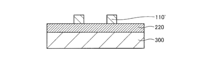
- FIG. 5 is a schematic cross-sectional view for explaining step (IV) in one embodiment of the method for producing an optical waveguide.
- FIG. 6 is a schematic cross-sectional view for explaining step (VI) in one embodiment of the method for producing an optical waveguide.
- FIG. 7 is a schematic cross-sectional view for explaining step (VII) in one embodiment of the method for producing an optical waveguide.
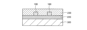
- FIG. 8 is a schematic cross-sectional view for explaining step (VIII) in one embodiment of the method for producing an optical waveguide.
- FIG. 9 is a schematic cross-sectional view for explaining step (IX) in one embodiment of the method for producing an optical waveguide.
- the resin sheet of the present invention has a support and a resin composition layer provided on the support.
- the thickness of the resin composition layer in the resin sheet of the present invention is not particularly limited, but from the viewpoint of thinning, it is preferably 250 ⁇ m or less, more preferably 200 ⁇ m or less, even more preferably 150 ⁇ m or less, and particularly preferably 100 ⁇ m or less.
- the lower limit of the thickness of the resin composition layer is not particularly limited, but it can be, for example, 5 ⁇ m or more, 10 ⁇ m or more, etc.
- the resin composition layer in the resin sheet according to the first embodiment of the present invention contains (A) a resin containing a carboxy group, (B) an epoxy resin, (C) a photopolymerization initiator, (D) a photocurable resin that does not contain a carboxy group, and (E) an organic solvent, and the parameter Y calculated by the following formula (1) has a numerical range of 2 to 20.
- a is the sum (mass %) of the content of component (A), the content of component (B), and the content of component (D) when all components other than component (E) in the resin composition layer are taken as 100 mass %
- b is the content (mass %) of organic solvents with a boiling point of 100°C or higher in component (E) when all components (E) in the resin composition layer are taken as 100 mass %
- c is the weight reduction rate (mass %) of the resin composition layer after the surface not in contact with the support is exposed to the outside air and heat-treated at 190°C for 30 minutes.
- the numerical range of parameter Y calculated by formula (1) is not particularly limited, but is preferably 2.5 to 20, more preferably 3.3 to 20, even more preferably 5 to 20, and particularly preferably 6.7 to 20.
- the resin composition layer in the resin sheet according to the second embodiment of the present invention contains (A) a resin containing a carboxy group, (B) an epoxy resin, (C) a photopolymerization initiator, (D) a photocurable resin not containing a carboxy group, and (E) an organic solvent, and the parameter X calculated by the following formula (2) has a numerical range of 5 to 50.
- a is the sum (mass %) of the content of component (A), the content of component (B), and the content of component (D) when all components in the resin composition layer except for component (E) are taken as 100 mass %
- b is the content (mass %) of organic solvents with a boiling point of 100°C or higher in component (E) when all components in the resin composition layer are taken as 100 mass %
- c is the weight reduction rate (mass %) of the resin composition layer after the surface not in contact with the support is exposed to the outside air and heat-treated at 190°C for 30 minutes.
- the numerical range of parameter X calculated by formula (2) is not particularly limited, but is preferably 5 to 40, more preferably 5 to 30, even more preferably 5 to 20, and particularly preferably 5 to 15.
- the resin composition layer in the resin sheet of the present invention may contain (A) a resin containing a carboxy group, (B) an epoxy resin, (C) a photopolymerization initiator, (D) a photocurable resin not containing a carboxy group, and (E) an organic solvent, as well as (F) a curing accelerator and (G) other additives.
- A a resin containing a carboxy group
- B an epoxy resin
- C a photopolymerization initiator
- D a photocurable resin not containing a carboxy group
- E an organic solvent
- the resin composition layer in the resin sheet of the present invention contains (A) a resin containing a carboxy group.
- the resin composition containing (A) a resin containing a carboxy group is soluble in an alkaline developer (e.g., a 1% by mass aqueous sodium carbonate solution) and can be developed in an alkaline state.
- the number of carboxy groups per molecule of (A) the resin containing a carboxy group may be one or two or more.
- the resin containing a carboxy group is not limited as long as it can be developed in an alkaline environment, but it is preferable that it further contains an ethylenically unsaturated group and/or an acetylenically unsaturated group, and it is particularly preferable that it contains an ethylenically unsaturated group.
- the ethylenically unsaturated group is a group having a carbon-carbon double bond
- the acetylenically unsaturated group is a group having a carbon-carbon triple bond.
- the resin containing a carboxy group is capable of photoradical polymerization when it contains an ethylenically unsaturated group.
- the number of ethylenically unsaturated groups per molecule of the resin containing a carboxy group may be one or more than two. Furthermore, when the (A) carboxyl group-containing resin contains two or more ethylenically unsaturated groups per molecule, those ethylenically unsaturated groups may be the same or different.
- the resin containing a carboxy group is preferably a resin that has both an ethylenically unsaturated group and a carboxy group, and that allows photoradical polymerization and alkaline development.
- Resin containing a carboxy group may be used alone or in combination of two or more types.
- (A) resin containing a carboxy group preferably contains a resin having an aromatic skeleton, more preferably contains a resin having a skeleton selected from a naphthalene skeleton and a biphenyl skeleton, even more preferably contains a resin having a naphthalene skeleton, and particularly preferably contains a resin having a naphthol aralkyl skeleton.
- the resin containing a carboxy group preferably contains an acid-modified epoxy (meth)acrylate resin.
- the acid-modified epoxy (meth)acrylate resin can be produced using an epoxy (meth)acrylate resin.
- the epoxy (meth)acrylate resin can be produced, for example, by reacting an epoxy resin with acrylic acid and/or methacrylic acid.
- Epoxy resins for producing epoxy (meth)acrylate resins are not particularly limited as long as they are compounds having an epoxy group in the molecule, and examples thereof include bisphenol-type epoxy resins such as bisphenol A-type epoxy resins, hydrogenated bisphenol A-type epoxy resins, bisphenol F-type epoxy resins, hydrogenated bisphenol F-type epoxy resins, bisphenol S-type epoxy resins, and modified bisphenol F-type epoxy resins obtained by reacting bisphenol F-type epoxy resins with epichlorohydrin to modify them to have three or more functional groups; biphenol-type epoxy resins, such as biphenol-type epoxy resins and tetramethylbiphenol-type epoxy resins; novolac-type epoxy resins such as phenol novolac-type epoxy resins, cresol novolac-type epoxy resins, bisphenol A-type novolac-type epoxy resins, and alkylphenol novolac-type epoxy resins; fluorine-containing epoxy resins such as bisphenol AF-type epoxy resins and perfluoroalky
- epoxy resins having a naphthalene skeleton such as binaphthol type epoxy resins, naphthylene ether type epoxy resins, naphthol novolac type epoxy resins, and naphthalene type epoxy resins obtained by a condensation reaction between polyhydroxynaphthalene and aldehydes (epoxy resins containing a naphthalene skeleton); bixylenol type epoxy resins; dicyclopentadiene type epoxy resins; trisphenol type epoxy resins; tert-butyl-catechol type epoxy resins; epoxy resins containing a condensed ring skeleton, such as anthracene type epoxy resins; glycidylamine type epoxy resins resins; glycidyl ester type epoxy resins; biphenyl type epoxy resins; linear aliphatic epoxy resins; epoxy resins having a butadiene structure; alicyclic epoxy resins; heterocyclic epoxy resins; spiro
- the epoxy resin for producing the epoxy (meth)acrylate resin is preferably an epoxy resin containing an aromatic skeleton from the viewpoint of reducing the average linear thermal expansion coefficient.
- the aromatic skeleton is a concept that includes polycyclic aromatics and aromatic heterocycles.
- any of cresol novolac type epoxy resin, bisphenol A type epoxy resin, bisphenol F type epoxy resin, biphenyl type epoxy resin, and naphthol aralkyl type epoxy resin is preferable.
- Acid-modified epoxy (meth)acrylate resins can be produced, for example, by reacting epoxy (meth)acrylate resins with polycarboxylic acid anhydrides.
- polyvalent carboxylic acid anhydrides examples include maleic anhydride, succinic anhydride, itaconic anhydride, phthalic anhydride, tetrahydrophthalic anhydride, hexahydrophthalic anhydride, trimellitic anhydride, pyromellitic anhydride, and benzophenonetetracarboxylic dianhydride, and these may be used alone or in combination of two or more.
- succinic anhydride and tetrahydrophthalic anhydride are preferred, and tetrahydrophthalic anhydride is more preferred.
- the acid-modified epoxy (meth)acrylate resin preferably contains an acid-modified epoxy (meth)acrylate resin having an aromatic skeleton, more preferably contains an acid-modified epoxy (meth)acrylate resin having a skeleton selected from a naphthalene skeleton and a biphenyl skeleton, even more preferably contains an acid-modified epoxy (meth)acrylate resin having a naphthalene skeleton, and particularly preferably contains an acid-modified epoxy (meth)acrylate resin having a naphthol aralkyl skeleton.
- the acid-modified epoxy (meth)acrylate resin can be synthesized by a known method, but commercially available products may also be used. Specific examples of commercially available products include "CCR-1373H” (acid-modified epoxy acrylate containing a cresol novolac skeleton), "ZCR-8001H” (acid-modified epoxy acrylate containing a biphenyl skeleton), “ZCR-1569H” (acid-modified epoxy acrylate containing a biphenyl skeleton), “ZCR-1761H” (acid-modified epoxy acrylate containing a biphenyl skeleton), “CCR-1171H” (acid-modified epoxy acrylate containing a cresol novolac skeleton), and “ZCR-1797H” (acid-modified epoxy acrylate containing a biphenyl skeleton), all manufactured by Nippon Kayaku Co., Ltd.
- Examples of such resins include "ZAR-2000” (bisphenol A skeleton-containing acid-modified epoxy acrylate resin), “ZFR-1491H”, and “ZFR-1533H” (bisphenol F skeleton-containing acid-modified epoxy acrylate resin) manufactured by Kayaku Co., Ltd., "PR-300CP” (cresol novolac type acid-modified epoxy acrylate resin) manufactured by Showa Denko KK, “CCR-1179” (cresol novolac skeleton-containing epoxy acrylate resin) manufactured by Nippon Kayaku Co., Ltd., and "(ACA)Z250” (acrylic copolymer type acid-modified epoxy acrylate resin) manufactured by Daicel-Allnex Corporation. These resins may be used alone or in combination of two or more.
- the acid value of (A) the resin containing a carboxy group is preferably 0.1 mgKOH/g or more, more preferably 0.5 mgKOH/g or more, even more preferably 1 mgKOH/g or more, 10 mgKOH/g or more, even more preferably 20 mgKOH/g or more, 30 mgKOH/g or more, and particularly preferably 40 mgKOH/g or more, 50 mgKOH/g or more, from the viewpoint of improving the alkaline developability of the resin composition layer.
- the upper limit of the acid value of (A) the resin containing a carboxy group is preferably 200 mgKOH/g or less, more preferably 150 mgKOH/g or less, even more preferably 120 mgKOH/g or less, and particularly preferably 100 mgKOH/g or less, from the viewpoint of improving the insulation reliability.
- the weight average molecular weight of the (A) resin containing a carboxy group is preferably 30,000 or less, more preferably 20,000 or less, even more preferably 10,000 or less, and particularly preferably 5,000 or less.
- the lower limit of the weight average molecular weight of the (A) resin containing a carboxy group is preferably 800 or more, more preferably 1,000 or more.
- the weight average molecular weight is the weight average molecular weight in terms of polystyrene measured by gel permeation chromatography (GPC).
- the content of the (A) carboxyl group-containing resin in the resin composition layer is preferably 5% by mass or more, more preferably 10% by mass or more, even more preferably 20% by mass or more, and particularly preferably 30% by mass or more, from the viewpoint of improving alkaline developability, when the non-volatile components in the resin composition layer (all components excluding (E) organic solvent) are taken as 100% by mass, and the upper limit is preferably 70% by mass or less, more preferably 60% by mass or less, even more preferably 50% by mass or less, and particularly preferably 40% by mass or less, from the viewpoint of improving heat resistance.
- the resin composition layer in the resin sheet of the present invention contains an epoxy resin (B).
- the epoxy resin (B) is a curable resin having an epoxy group.
- epoxy resins examples include bixylenol type epoxy resins, bisphenol A type epoxy resins, bisphenol F type epoxy resins, bisphenol S type epoxy resins, bisphenol AF type epoxy resins, dicyclopentadiene type epoxy resins, trisphenol type epoxy resins, naphthol novolac type epoxy resins, phenol novolac type epoxy resins, tert-butyl-catechol type epoxy resins, naphthalene type epoxy resins, naphthol type epoxy resins, anthracene type epoxy resins, glycidylamine type epoxy resins, glycidyl ester type epoxy resins, cresol novolac type epoxy resins,
- the epoxy resin include phenol aralkyl type epoxy resin, biphenyl type epoxy resin, linear aliphatic epoxy resin, epoxy resin having a butadiene structure, alicyclic epoxy resin, heterocyclic epoxy resin, spiro ring-containing epoxy resin, cyclohexane type epoxy resin,
- the resin composition layer of the present invention preferably contains, as the epoxy resin (B), an epoxy resin having two or more epoxy groups in one molecule.
- the ratio of the epoxy resin having two or more epoxy groups in one molecule relative to 100% by mass of the epoxy resin (B) is preferably 50% by mass or more, more preferably 60% by mass or more, and particularly preferably 70% by mass or more.
- Epoxy resins include epoxy resins that are liquid at a temperature of 20°C (hereinafter sometimes referred to as “liquid epoxy resins”) and epoxy resins that are solid at a temperature of 20°C (hereinafter sometimes referred to as “solid epoxy resins”).
- the resin composition layer of the present invention may contain only liquid epoxy resins as epoxy resins, or only solid epoxy resins, or both liquid and solid epoxy resins, but it is particularly preferable that the resin composition layer contains only solid epoxy resins or both liquid and solid epoxy resins.
- the liquid epoxy resin is preferably one that has two or more epoxy groups in one molecule.
- Preferred liquid epoxy resins are glycirol type epoxy resins, bisphenol A type epoxy resins, bisphenol F type epoxy resins, bisphenol AF type epoxy resins, naphthalene type epoxy resins, glycidyl ester type epoxy resins, glycidyl amine type epoxy resins, phenol novolac type epoxy resins, alicyclic epoxy resins having an ester skeleton, cyclohexane dimethanol type epoxy resins, cyclic aliphatic glycidyl ethers, and epoxy resins having a butadiene structure, dicyclopentadiene type epoxy resins, epoxy resins containing an alkyleneoxy skeleton, and epoxy resins containing a fluorene structure.
- liquid epoxy resins include Nagase ChemteX's "EX-992L,” Mitsubishi Chemical's “YX7400,” DIC's “HP4032,” “HP4032D,” and “HP4032SS” (naphthalene-type epoxy resins); Mitsubishi Chemical's “828US,” “jER828EL,” “828EL,” “825,” and “Epicoat 828EL,” DIC's "850” (bisphenol A-type epoxy resin); Mitsubishi Chemical's "jER 807, 1750 (bisphenol F type epoxy resin); Mitsubishi Chemical's jER152 (phenol novolac type epoxy resin); Mitsubishi Chemical's 630, 630LSD, 604 (glycidylamine type epoxy resin); ADEKA's ED-523T (glycilol type epoxy resin); ADEKA's EP-3950L, EP-3980S (glycidylamine type epoxy resin); ADEKA's EP-4 088S (dicyclopentadiene type epoxy resin); "Z
- solid epoxy resin a solid epoxy resin having three or more epoxy groups in one molecule is preferable, and an aromatic solid epoxy resin having three or more epoxy groups in one molecule is more preferable.
- Preferred solid epoxy resins are bixylenol type epoxy resins, naphthalene type epoxy resins, naphthalene type tetrafunctional epoxy resins, naphthol novolac type epoxy resins, cresol novolac type epoxy resins, dicyclopentadiene type epoxy resins, trisphenol type epoxy resins, naphthol type epoxy resins, biphenyl type epoxy resins, naphthylene ether type epoxy resins, anthracene type epoxy resins, bisphenol A type epoxy resins, bisphenol AF type epoxy resins, phenol aralkyl type epoxy resins, tetraphenylethane type epoxy resins, phenolphthalimidine type epoxy resins, and fluorene structure-containing epoxy resins.
- solid epoxy resins include DIC's "HP4032H” (naphthalene type epoxy resin); DIC's “HP-4700” and “HP-4710” (naphthalene type tetrafunctional epoxy resin); DIC's "N-690” and “N-695" (cresol novolac type epoxy resin); DIC's "HP-7200”, “HP-7200HH”, “HP-7200H”, and “HP-7200L” (dicyclopentadiene type epoxy resin); and DIC's "EXA-7311” and "EXA-7311-G3".
- the (B) epoxy resin preferably contains an epoxy resin having an aromatic skeleton, more preferably contains an epoxy resin having a skeleton selected from a naphthalene skeleton and a biphenyl skeleton, even more preferably contains an epoxy resin having a naphthalene skeleton, and particularly preferably contains an epoxy resin having a naphthol aralkyl skeleton.
- the (B) epoxy resin contains an epoxy resin having the same backbone (preferably a naphthalene backbone, and particularly preferably a naphthol aralkyl backbone) as the (A) carboxyl group-containing resin.
- the epoxy equivalent of the (B) epoxy resin is preferably 50 g/eq. to 5,000 g/eq., more preferably 60 g/eq. to 2,000 g/eq., even more preferably 70 g/eq. to 1,000 g/eq., and even more preferably 80 g/eq. to 500 g/eq.
- the epoxy equivalent is the mass of resin per equivalent of epoxy groups. This epoxy equivalent can be measured in accordance with JIS K7236.
- the weight average molecular weight (Mw) of the (B) epoxy resin is preferably 100 to 5,000, more preferably 250 to 3,000, and even more preferably 400 to 1,500.
- the weight average molecular weight of the resin can be measured as a polystyrene-equivalent value by gel permeation chromatography (GPC).
- the content of the (B) epoxy resin in the resin composition layer is preferably 5% by mass or more, more preferably 10% by mass or more, even more preferably 20% by mass or more, and particularly preferably 30% by mass or more, from the viewpoint of further improving the mechanical strength and insulation reliability, and the upper limit is preferably 70% by mass or less, more preferably 60% by mass or less, even more preferably 50% by mass or less, and particularly preferably 40% by mass or less.
- the mass ratio of the resin containing a carboxy group (A) to the epoxy resin (B) in the resin composition layer (component (A)/component (B)) is preferably 0.1 or more, more preferably 0.5 or more, and even more preferably 0.8 or more.
- the upper limit is preferably 10 or less, more preferably 3 or less, and even more preferably 1.5 or less.
- the resin composition layer in the resin sheet of the present invention contains a photopolymerization initiator (C).
- Examples of the (C) photopolymerization initiator include ⁇ -aminoketone-based photopolymerization initiators, phosphine oxide-based photopolymerization initiators, ⁇ -hydroxyketone-based photopolymerization initiators, oxime ester-based photopolymerization initiators, benzoin-based photopolymerization initiators, and benzyl ketal-based photopolymerization initiators.
- the resin composition layer in the resin sheet of the present invention preferably contains, as the (C) photopolymerization initiator, a photopolymerization initiator selected from ⁇ -aminoketone-based photopolymerization initiators and phosphine oxide-based photopolymerization initiators, and more preferably contains an ⁇ -aminoketone-based photopolymerization initiator.
- phosphine oxide photopolymerization initiators include bis(2,4,6-trimethylbenzoyl)phenylphosphine oxide, (2,4,6-trimethylbenzoyl)diphenylphosphine oxide, polyoxyethylene glycerin ether tris[phenyl(2,4,6-trimethylbenzoyl)phosphinate] (Polymeric TPO-L), etc.
- Examples of ⁇ -hydroxyketone photopolymerization initiators include 1-hydroxycyclohexyl phenyl ketone, 2-hydroxy-2-methyl-1-phenylpropanone, 1-[4-(2-hydroxyethoxy)phenyl]-2-hydroxy-2-methylpropanone, 2-hydroxy-1- ⁇ 4-[4-(2-hydroxy-2-methylpropionyl)benzyl]phenyl ⁇ -2-methylpropan-1-one, etc.
- oxime ester photopolymerization initiators examples include 2-(benzoyloxyimino)-1-[4-(phenylthio)phenyl]octan-1-one (OXE01) and [1-[9-ethyl-6-(2-methylbenzoyl)carbazol-3-yl]ethylideneamino]acetate (OXE02).
- benzoin-based photopolymerization initiators examples include benzoin, benzoin methyl ether, benzoin ethyl ether, benzoin isopropyl ether, and benzoin isobutyl ether.
- benzoin-based photopolymerization initiators examples include 2,2-dimethoxy-2-phenylacetophenone.
- Examples of ⁇ -aminoketone photopolymerization initiators include 2-methyl-1-phenyl-2-morpholinopropan-1-one, 2-methyl-1-[4-(methylthio)phenyl]-2-morpholinopropan-1-one, 2-methyl-1-(4-hexylphenyl)-2-morpholinopropan-1-one, 2-ethyl-2-(dimethylamino)-1-(4-morpholinophenyl)butan-1-one, 2-benzyl-2-(dimethylamino)-1-(4-morpholinophenyl)butan-1-one, and 2-dimethylamino-2-(4-methyl-benzyl)-1-(4-morpholin-4-yl-phenyl)-butan-1-one.
- the content of the (C) photopolymerization initiator in the resin composition layer is preferably 0.1% by mass or more, more preferably 0.5% by mass or more, even more preferably 1% by mass or more, and particularly preferably 2% by mass or more, with the upper limit being preferably 20% by mass or less, more preferably 15% by mass or less, even more preferably 10% by mass or less, and particularly preferably 5% by mass or less, when the non-volatile components in the resin composition layer (all components excluding the (E) organic solvent) are taken as 100% by mass.
- the resin composition layer in the resin sheet of the present invention contains (D) a photocurable resin that does not contain a carboxy group.
- a photocurable resin that does not contain a carboxy group for example, a photosensitive (meth)acrylate compound having one or more (meth)acryloyl groups in one molecule can be used.
- the (D) photocurable resin that does not contain a carboxy group may be used alone or in combination of two or more.
- the (D) component does not include those that correspond to the (B) component.
- Representative photosensitive (meth)acrylate compounds include, for example, hydroxyalkyl (meth)acrylates such as 2-hydroxyethyl (meth)acrylate and 2-hydroxybutyl (meth)acrylate; mono- or di(meth)acrylates of glycols such as ethylene glycol, methoxytetraethylene glycol, polyethylene glycol, and propylene glycol; (meth)acrylamides such as N,N-dimethyl(meth)acrylamide and N-methylol(meth)acrylamide; aminoalkyl (meth)acrylates such as N,N-dimethylaminoethyl (meth)acrylate; trimethylolpropane; Examples of such compounds include polyhydric (meth)acrylates of polyhydric alcohols such as polypentaerythritol, pentaerythritol, and dipentaerythritol, or their adducts with ethylene oxide, propylene oxide, or ⁇ -caprolactone; (me
- trivalent or higher (meth)acrylates include trimethylolpropane tri(meth)acrylate, pentaerythritol tri(meth)acrylate, trimethylolpropane EO-added tri(meth)acrylate, glycerin PO-added tri(meth)acrylate, pentaerythritol tetra(meth)acrylate, 1,4-butanediol oligo(meth)acrylate, 1,6-hexanediol oligo(meth)acrylate, trimethylolpropane oligo(meth)acrylate, pentaerythritol oligo(meth)acrylate, tetramethylolmethane tetra(meth)acrylate, dipentaerythritol hexa(meth)acrylate, and (meth)
- the trivalent or higher (meth)acrylate may be a trivalent or higher phosphoric acid triester (meth)acrylate.
- Examples of the trivalent or higher phosphoric acid triester (meth)acrylate include tri(2-(meth)acryloyloxyethyl)phosphate, tri(2-(meth)acryloyloxypropyl)phosphate, tri(3-(meth)acryloyloxypropyl)phosphate, tri(3-(meth)acryloyl-2-hydroxyloxypropyl)phosphate, di(3-(meth)acryloyl-2-hydroxyloxypropyl)(2-(meth)acryloyloxyethyl)phosphate, and (3-(meth)acryloyl-2-hydroxyloxypropyl)di(2-(meth)acryloyloxyethyl)phosphate.
- These photosensitive (meth)acrylate compounds may be used alone or in combination of two or more.
- a commercially available photocurable resin that does not contain a carboxy group can be used.
- Examples of commercially available products include "DPHA” manufactured by Nippon Kayaku Co., Ltd. and “EBECRYL3708” manufactured by Daicel-Allnex Co., Ltd.
- the molecular weight of the photocurable resin not containing a carboxy group is not particularly limited, but the upper limit is preferably 5,000 or less, more preferably 3,000 or less, even more preferably 2,000 or less, even more preferably 1,500 or less, even more preferably 1,000 or less, and especially preferably 700 or less, and the lower limit is preferably 50 or more, more preferably 75 or more, even more preferably 100 or more, even more preferably 200 or more, even more preferably 300 or more, and especially preferably 400 or more.
- the content of the (D) photocurable resin not containing a carboxy group in the resin composition layer is preferably 1% by mass or more, more preferably 5% by mass or more, even more preferably 10% by mass or more, and particularly preferably 20% by mass or more, with the upper limit being preferably 50% by mass or less, more preferably 40% by mass or less, even more preferably 35% by mass or less, and particularly preferably 30% by mass or less, when the nonvolatile components in the resin composition layer (all components excluding (E) organic solvent) are taken as 100% by mass, and the content is preferably 50% by mass or less, more preferably 40% by mass or less, even more preferably 35% by mass or less, and particularly preferably 30% by mass or less.
- the total content of (A) the resin containing a carboxy group, (B) the epoxy resin, and (D) the photocurable resin not containing a carboxy group is preferably 80% by mass or more, more preferably 85% by mass or more, even more preferably 90% by mass or more, and particularly preferably 95% by mass or more, when the non-volatile components in the resin composition layer (all components excluding (E) the organic solvent) are taken as 100% by mass.
- the resin composition layer in the resin sheet of the present invention contains an organic solvent (E).
- the organic solvent (E) described here is a liquid compound (a compound that is liquid at room temperature (25°C)) that is composed of skeletal atoms selected from carbon atoms and oxygen atoms and hydrogen atoms as non-skeletal atoms, and does not contain carbon-carbon triple bonds or carbon-carbon double bonds (except for bonds that constitute aromatic rings) in the molecule and has a boiling point of 250°C or less.
- the organic solvent (E) described here does not include those that correspond to the epoxy resin (B).
- the boiling point refers to the boiling point (i.e., normal boiling point) under normal pressure (1 atm; 760 mmHg).
- the organic solvent (E) may be used alone or in combination of two or more types.
- organic solvents examples include glycol-based solvents, glycol ether-based solvents, glycol ether ester-based solvents, ketone-based solvents, ester-based solvents, ether-based solvents, alcohol-based solvents, aliphatic hydrocarbon-based solvents, and aromatic hydrocarbon-based solvents.
- glycol-based solvents examples include ethylene glycol (boiling point 197°C), diethylene glycol (boiling point 244°C), propylene glycol (boiling point 188°C), dipropylene glycol (boiling point 232°C), trimethylene glycol (boiling point 214°C), etc.
- Glycol ether solvents include, for example, cellosolves such as ethylene glycol monomethyl ether (also known as methyl cellosolve) (boiling point 124°C), ethylene glycol monoethyl ether (also known as cellosolve) (boiling point 135°C), ethylene glycol monopropyl ether (also known as propyl cellosolve) (boiling point 151°C), ethylene glycol monobutyl ether (also known as butyl cellosolve) (boiling point 171°C), ethylene glycol monoisobutyl ether (also known as isobutyl cellosolve) (boiling point 160°C), ethylene glycol mono-tert-butyl ether (also known as tert-butyl cellosolve) (boiling point 152°C), and ethylene glycol monohexyl ether (boiling point 208°C); diethylene glycol monomethyl ether
- Glycol ether ester solvents include, for example, cellosolve esters such as ethylene glycol monomethyl ether acetate (also known as methyl cellosolve acetate) (boiling point 145°C), ethylene glycol monoethyl ether acetate (also known as cellosolve acetate) (boiling point 156°C), and ethylene glycol monobutyl ether acetate (also known as butyl cellosolve acetate) (boiling point 191°C); diethylene glycol monoethyl ether acetate (EDGAc) (also known as carbitol acetate) ( carbitol esters such as diethylene glycol monobutyl ether acetate (also known as butyl carbitol acetate) (boiling point 247°C); propylene glycol ether esters such as propylene glycol monomethyl ether acetate (PGMEAc) (boiling point 146°C)
- Ketone solvents include, for example, aliphatic acyclic ketones such as acetone (boiling point 56°C), methyl ethyl ketone (MEK) (boiling point 79°C), diethyl ketone (boiling point 101°C), 2-pentanone (boiling point 101°C), methyl isobutyl ketone (boiling point 116°C), 2-hexanone (boiling point 127°C), 2-heptanone (MAK) (boiling point 151°C), and diisobutyl ketone (boiling point 168°C); aliphatic cyclic ketones such as cyclopentanone (boiling point 131°C), cyclohexanone (anone) (boiling point 155°C), and 2-methylcyclohexanone (boiling point 162°C); and aromatic ketones such as acetophenone (boil
- Ester solvents are solvents that have an ester structure that does not fall under the category of glycol ether ester solvents, such as methyl acetate (boiling point 57°C), ethyl acetate (boiling point 77°C), n-propyl acetate (boiling point 96°C), isopropyl acetate (boiling point 89°C), n-butyl acetate (boiling point 126°C), isobutyl acetate (boiling point 118°C), sec-butyl acetate (boiling point 112°C), tert-butyl acetate (boiling point 97°C), n-pentyl acetate (boiling point 149°C), isopentyl acetate (boiling point 142°C), ethyl propionate (boiling point 99°C), and propionate.
- alkyl esters examples include fatty acid alkyl esters such as propyl lactate (boiling point 122°C) and isopropyl propionate (boiling point 108°C); hydroxy acid alkyl esters such as methyl lactate (boiling point 144°C), ethyl lactate (boiling point 154°C), and butyl lactate (boiling point 187°C); keto acid alkyl esters such as methyl acetoacetate (boiling point 170°C) and ethyl acetoacetate (boiling point 184°C); lactones such as ⁇ -butyrolactone (boiling point 204°C); and aromatic esters such as methyl benzoate (boiling point 200°C) and ethyl benzoate (boiling point 212°C).
- fatty acid alkyl esters such as propyl lactate (boiling point 122°C
- Ether solvents are solvents with an ether structure that do not fall under the category of glycol ether solvents or glycol ether ester solvents, and examples of such solvents include aliphatic acyclic ethers such as diethyl ether (boiling point 34°C), diisopropyl ether (boiling point 68°C), and methyl tert-butyl ether (boiling point 55°C); aliphatic cyclic ethers such as tetrahydrofuran (boiling point 66°C), 1,4-dioxane (boiling point 101°C), and 1,3-dioxolane (boiling point 75°C); and aromatic ethers such as anisole (boiling point 154°C) and phenetole (boiling point 169°C).
- aliphatic acyclic ethers such as diethyl ether (boiling point 34°C), diiso
- Alcohol-based solvents are solvents that have an alcohol structure that does not fall under the category of glycol-based solvents or glycol ether-based solvents, and examples of such solvents include methanol (boiling point 64°C), ethanol (boiling point 78°C), n-propanol (boiling point 97°C), isopropanol (boiling point 82°C), n-butyl alcohol (boiling point 117°C), isobutyl alcohol (boiling point 108°C), sec-butyl alcohol (boiling point 99°C), tert-butyl alcohol (boiling point 82°C), n-pentyl alcohol (boiling point 138°C), isopentyl alcohol (boiling point 131°C), sec-pentyl alcohol (aliphatic acyclic alcohols such as 2-ethylhexyl alcohol (boiling point 184°C), tert
- Aliphatic hydrocarbon solvents include, for example, n-pentane (boiling point 36°C), n-hexane (boiling point 69°C), 2-methylpentane (also known as isohexane) (boiling point 60°C), n-heptane (boiling point 98°C), n-octane (boiling point 125°C), cyclopentane (boiling point 49°C), cyclohexane (boiling point 81°C), methylcyclohexane (boiling point 101°C), and ethylcyclohexane (boiling point 132°C).
- aromatic hydrocarbon solvents include C6-8 aromatic hydrocarbons such as benzene (boiling point 80° C.), toluene (boiling point 110° C.), o-xylene (boiling point 144° C.), m-xylene (boiling point 139° C.), p - xylene (boiling point 138° C.), and ethylbenzene (boiling point 136° C.); C1,2,3-trimethylbenzene (boiling point 176° C.), 1,3,5-trimethylbenzene (boiling point 165° C.), 1,2,4-trimethylbenzene (boiling point 169° C.), 4-ethyltoluene (boiling point 161° C.), 3-ethyltoluene (boiling point 160° C.), and 2-ethyltoluene (boiling point 166° C.).
- C10 aromatic hydrocarbons such as 1,2-diethylbenzene (boiling point 184°C), 1,3-diethylbenzene (boiling point 181°C), 1,4-diethylbenzene (boiling point 183°C), 3-ethyl-o-xylene (boiling point 194°C), 4-ethyl-o-xylene (boiling point 190°C), 2-ethyl-p-xylene (boiling point 187°C), and 1,2,3,5 -tetramethylbenzene (boiling point 198°C).
- the organic solvent preferably includes an organic solvent selected from glycol-based solvents, glycol ether-based solvents, glycol ether ester-based solvents, ketone-based solvents, ester-based solvents, ether-based solvents, and alcohol-based solvents, and more preferably includes an organic solvent selected from glycol-based solvents, glycol ether-based solvents, glycol ether ester-based solvents, and ketone-based solvents.
- an organic solvent selected from glycol-based solvents, glycol ether-based solvents, glycol ether ester-based solvents, and ketone-based solvents, it becomes easier to adjust the numerical range of parameter Y calculated by formula (1) to 2 to 20, and it becomes easier to adjust the numerical range of parameter X calculated by formula (2) to 5 to 50.
- the content of the organic solvent having a boiling point of 100°C or higher in the (E) organic solvent contained in the resin composition layer in the resin sheet of the present invention is preferably 50% by mass to 100% by mass, more preferably 60% by mass to 100% by mass, even more preferably 70% by mass to 100% by mass, even more preferably 80% by mass to 100% by mass, and particularly preferably 85% by mass to 100% by mass, assuming that the total (E) organic solvent in the resin composition layer is 100% by mass.
- the content of the organic solvent having a boiling point of less than 100°C in the (E) organic solvent contained in the resin composition layer in the resin sheet of the present invention is preferably 0% by mass to 50% by mass, more preferably 0% by mass to 40% by mass, even more preferably 0% by mass to 30% by mass, even more preferably 0% by mass to 20% by mass, and particularly preferably 0% by mass to 15% by mass, assuming that the total (E) organic solvent in the resin composition layer is 100% by mass.
- the content of the organic solvent having a boiling point of 200°C or higher in the (E) organic solvent contained in the resin composition layer in the resin sheet of the present invention is preferably 0% by mass to 30% by mass, more preferably 0% by mass to 20% by mass, even more preferably 0% by mass to 10% by mass, even more preferably 0% by mass to 5% by mass, and particularly preferably 0% by mass to 1% by mass, assuming that the total (E) organic solvent in the resin composition layer is 100% by mass.
- the content of the organic solvent selected from ester-based solvents in the (E) organic solvent contained in the resin composition layer in the resin sheet of the present invention is preferably 0% by mass to 50% by mass, more preferably 0% by mass to 20% by mass, even more preferably 0% by mass to 10% by mass, even more preferably 0% by mass to 5% by mass, and particularly preferably 0% by mass to 1% by mass, when the total (E) organic solvent in the resin composition layer is taken as 100% by mass.
- the content of the organic solvent selected from ether-based solvents in the (E) organic solvent contained in the resin composition layer in the resin sheet of the present invention is preferably 0% by mass to 50% by mass, more preferably 0% by mass to 20% by mass, even more preferably 0% by mass to 10% by mass, even more preferably 0% by mass to 5% by mass, and particularly preferably 0% by mass to 1% by mass, when the total (E) organic solvent in the resin composition layer is taken as 100% by mass.
- the content of the alcohol-based solvent in the (E) organic solvent contained in the resin composition layer in the resin sheet of the present invention is preferably 0% by mass to 50% by mass, more preferably 0% by mass to 20% by mass, even more preferably 0% by mass to 10% by mass, even more preferably 0% by mass to 5% by mass, and particularly preferably 0% by mass to 1% by mass, assuming that the total (E) organic solvent in the resin composition layer is 100% by mass.
- the content of the aliphatic hydrocarbon solvent in the (E) organic solvent contained in the resin composition layer in the resin sheet of the present invention is preferably 0% by mass to 50% by mass, more preferably 0% by mass to 20% by mass, even more preferably 0% by mass to 10% by mass, even more preferably 0% by mass to 5% by mass, and particularly preferably 0% by mass to 1% by mass, assuming that the total (E) organic solvent in the resin composition layer is 100% by mass.
- the content of aromatic hydrocarbon solvents in the (E) organic solvent contained in the resin composition layer in the resin sheet of the present invention is preferably 0% by mass to 50% by mass, more preferably 0% by mass to 20% by mass, even more preferably 0% by mass to 10% by mass, even more preferably 0% by mass to 5% by mass, and particularly preferably 0% by mass to 1% by mass, assuming that the total (E) organic solvent in the resin composition layer is 100% by mass.
- the content of aromatic solvents (solvents having an aromatic ring, including aromatic ketones, aromatic esters, aromatic ethers, aromatic alcohols, and aromatic hydrocarbon solvents) in the (E) organic solvent contained in the resin composition layer in the resin sheet of the present invention is preferably 0% by mass to 50% by mass, more preferably 0% by mass to 20% by mass, even more preferably 0% by mass to 10% by mass, even more preferably 0% by mass to 5% by mass, and particularly preferably 0% by mass to 1% by mass, assuming that the total (E) organic solvent in the resin composition layer is 100% by mass.
- the content of the (E) organic solvent in the resin composition layer in the resin sheet of the present invention can be set so that the weight loss rate of the resin composition layer after the surface of the resin sheet that is not in contact with the support is exposed to the outside air (the other surface is the laminated surface with the support) and heat-treated at 190°C (under normal pressure) for 30 minutes is preferably 30% by mass or less, more preferably 25% by mass or less, even more preferably 20% by mass or less, particularly preferably 16% by mass or less, with the lower limit being preferably 1% by mass or more, more preferably 3% by mass or more, even more preferably 5% by mass or more, even more preferably 7% by mass or more, particularly preferably 8% by mass or more.
- the content of (E) organic solvent in the resin composition layer is not particularly limited, but when all components in the resin composition layer are taken as 100% by mass, it is preferably 30% by mass or less, more preferably 25% by mass or less, even more preferably 20% by mass or less, and particularly preferably 16% by mass or less, and the lower limit is preferably 1% by mass or more, more preferably 3% by mass or more, even more preferably 5% by mass or more, even more preferably 7% by mass or more, and particularly preferably 8% by mass or more.
- the resin composition layer in the resin sheet of the present invention may contain a curing accelerator (F) as an optional component.
- the curing accelerator (F) functions as a curing catalyst that accelerates the curing of the epoxy resin (B).
- the curing accelerator examples include phosphorus-based curing accelerators, urea-based curing accelerators, guanidine-based curing accelerators, imidazole-based curing accelerators, metal-based curing accelerators, and amine-based curing accelerators.
- the curing accelerator preferably contains a curing accelerator selected from imidazole-based curing accelerators and amine-based curing accelerators, and more preferably contains an imidazole-based curing accelerator.
- the curing accelerator may be used alone or in combination of two or more types.
- Examples of phosphorus-based curing accelerators include aliphatic phosphonium salts such as tetrabutylphosphonium bromide, tetrabutylphosphonium chloride, tetrabutylphosphonium acetate, tetrabutylphosphonium decanoate, tetrabutylphosphonium laurate, bis(tetrabutylphosphonium)pyromellitate, tetrabutylphosphonium hydrogenhexahydrophthalate, tetrabutylphosphonium 2,6-bis[(2-hydroxy-5-methylphenyl)methyl]-4-methylphenolate, and di-tert-butylmethylphosphonium tetraphenylborate; methyltriphenylphosphonium bromide, ethyltriphenylphosphonium bromide, propyltriphenylphosphonium bromide, butyltriphenylphosphonium bromide, benzyltriphenylphosphonium
- urea-based hardening accelerators include 1,1-dimethylurea; aliphatic dimethylureas such as 1,1,3-trimethylurea, 3-ethyl-1,1-dimethylurea, 3-cyclohexyl-1,1-dimethylurea, and 3-cyclooctyl-1,1-dimethylurea; 3-phenyl-1,1-dimethylurea, 3-(4-chlorophenyl)-1,1-dimethylurea, 3-(3,4-dichlorophenyl)-1,1-dimethylurea, 3-(3-chloro-4-methylphenyl)-1,1-dimethylurea, 3-(2-methylphenyl)-1,1-dimethylurea, 3-(4-methylphenyl)-1,1-dimethylurea, and 3-(3,4-dimethylphenyl)-1,1-dimethylurea.
- aromatic dimethylureas include toluene bis(dimethylurea), 3-(4-isopropylphenyl)-1,1-dimethylurea, 3-(4-methoxyphenyl)-1,1-dimethylurea, 3-(4-nitrophenyl)-1,1-dimethylurea, 3-[4-(4-methoxyphenoxy)phenyl]-1,1-dimethylurea, 3-[4-(4-chlorophenoxy)phenyl]-1,1-dimethylurea, 3-[3-(trifluoromethyl)phenyl]-1,1-dimethylurea, N,N-(1,4-phenylene)bis(N',N'-dimethylurea), and N,N-(4-methyl-1,3-phenylene)bis(N',N'-dimethylurea) [toluene bisdimethylurea].
- guanidine-based curing accelerators include dicyandiamide, 1-methylguanidine, 1-ethylguanidine, 1-cyclohexylguanidine, 1-phenylguanidine, 1-(o-tolyl)guanidine, dimethylguanidine, diphenylguanidine, trimethylguanidine, tetramethylguanidine, pentamethylguanidine, 1,5,7-triazabicyclo[4.4.0]dec-5-ene, 7-methyl-1,5,7-triazabicyclo[4.4.0]dec-5-ene, 1-methylbiguanide, 1-ethylbiguanide, 1-n-butylbiguanide, 1-n-octadecylbiguanide, 1,1-dimethylbiguanide, 1,1-diethylbiguanide, 1-cyclohexylbiguanide, 1-allylbiguanide, 1-phenylbiguanide, and 1-(o-tolyl)biguan
- imidazole-based hardening accelerators examples include 2-methylimidazole, 2-undecylimidazole, 2-heptadecylimidazole, 1,2-dimethylimidazole, 2-ethyl-4-methylimidazole, 2-phenylimidazole, 2-phenyl-4-methylimidazole, 1-benzyl-2-methylimidazole, 1-benzyl-2-phenylimidazole, and 1-cyanoethyl-2-methylimidazole.
- imidazole-based curing accelerators commercially available products may be used, such as "1B2PZ”, “2MZA-PW”, “2PHZ-PW”, and “C11Z-A” manufactured by Shikoku Chemical Industry Co., Ltd., and "P200-H50” manufactured by Mitsubishi Chemical Corporation.
- Metal-based curing accelerators include, for example, organometallic complexes or organometallic salts of metals such as cobalt, copper, zinc, iron, nickel, manganese, and tin.
- organometallic complexes include organocobalt complexes such as cobalt(II) acetylacetonate and cobalt(III) acetylacetonate, organocopper complexes such as copper(II) acetylacetonate, organozinc complexes such as zinc(II) acetylacetonate, organoiron complexes such as iron(III) acetylacetonate, organonickel complexes such as nickel(II) acetylacetonate, and organomanganese complexes such as manganese(II) acetylacetonate.
- organometallic salts include zinc octoate, tin octoate, zinc naphthenate,
- Amine-based curing accelerators include, for example, trialkylamines such as triethylamine and tributylamine, 4-dimethylaminopyridine, benzyldimethylamine, 2,4,6-tris(dimethylaminomethyl)phenol, and 1,8-diazabicyclo(5,4,0)-undecene.
- Amine-based curing accelerators may be commercially available products, such as "MY-25” manufactured by Ajinomoto Fine-Techno Co., Ltd.
- the content of the (F) curing accelerator in the resin composition layer is not particularly limited, but is preferably 5% by mass or less, more preferably 3% by mass or less, even more preferably 1% by mass or less, and particularly preferably 0.7% by mass or less, when the non-volatile components in the resin composition layer (all components excluding the (E) organic solvent) are taken as 100% by mass.
- the lower limit of the content of the (F) curing accelerator in the resin composition layer is not particularly limited, but may be, for example, 0% by mass or more, 0.001% by mass or more, 0.01% by mass or more, 0.1% by mass or more, 0.3% by mass or more, when the non-volatile components in the resin composition layer (all components excluding the (E) organic solvent) are taken as 100% by mass.
- the resin composition layer in the resin sheet of the present invention may further contain (G) other additives to the extent that the object of the present invention is not impaired.
- G) Other additives include, for example, active ester curing agents, phenolic curing agents, naphthol curing agents, carbodiimide curing agents, acid anhydride curing agents, amine curing agents, benzoxazine curing agents, cyanate ester curing agents, and other epoxy resin curing agents; inorganic fillers such as silica, alumina, and aluminosilicates; photosensitizers such as benzophenones; thermoplastic resins, organic fillers, fine particles such as melamine and organic bentonite; colorants such as phthalocyanine blue, phthalocyanine green, iodine green, diazo yellow, crystal violet, titanium oxide, carbon black, and naphthalene black; polymerization inhibitors such as hydroquinone, phenothiazin
- the components (A) to (F) may have functions such as a curing agent, a photosensitizer, fine particles, a colorant, a polymerization inhibitor, a thickener, an antifoaming agent, and a flame retardant.
- the component is regarded as each of the components (A) to (F) rather than as the component (G).
- the component (B) having a function as a flame retardant includes a brominated epoxy compound and an acid-modified brominated epoxy compound.
- the resin sheet of the present invention has a support.
- the support in the resin sheet of the present invention include a film made of a plastic material, a metal foil, and a release paper, and a film made of a plastic material and a metal foil are preferred.
- plastic material examples include polyesters such as polyethylene terephthalate (hereinafter sometimes abbreviated as “PET”) and polyethylene naphthalate (hereinafter sometimes abbreviated as “PEN”), polycarbonate (hereinafter sometimes abbreviated as “PC”), acrylic polymers such as polymethyl methacrylate (PMMA), cyclic polyolefins, triacetyl cellulose (TAC), polyether sulfide (PES), polyether ketone, polyimide, etc.
- PET polyethylene terephthalate
- PEN polyethylene naphthalate
- PC polycarbonate
- acrylic polymers such as polymethyl methacrylate (PMMA), cyclic polyolefins, triacetyl cellulose (TAC), polyether sulfide (PES), polyether ketone, polyimide, etc.
- PMMA polymethyl methacrylate
- TAC triacetyl cellulose
- PES polyether sulfide
- polyether ketone
- examples of the metal foil include copper foil and aluminum foil, with copper foil being preferred.
- the copper foil foil made of a single metal, copper, or an alloy of copper and another metal (e.g., tin, chromium, silver, magnesium, nickel, zirconium, silicon, titanium, etc.) may be used.
- the support may be subjected to a matte treatment or corona treatment on the surface that is to be bonded to the resin composition layer.
- a support with a release layer having a release layer on the surface to be bonded to the resin composition layer may be used.
- the release agent used in the release layer of the support with a release layer include one or more release agents selected from the group consisting of alkyd-based release agents, polyolefin-based release agents, urethane-based release agents, and silicone-based release agents.
- PET501010 Commercially available products may be used as the support with a release layer, and examples of such products include “PET501010", “SK-1”, “AL-5”, and “AL-7” manufactured by Lintec Corporation, “Lumirror T60” and “Lumirror T6AM” manufactured by Toray Industries, Inc., “Purex” manufactured by Teijin Limited, and “Unipeel” manufactured by Unitika Limited, which are PET films having a release layer mainly composed of a silicone-based release agent or an alkyd resin-based release agent.
- the thickness of the support is not particularly limited, but is preferably in the range of 5 ⁇ m to 75 ⁇ m, and more preferably in the range of 10 ⁇ m to 60 ⁇ m. When using a support with a release layer, it is preferable that the thickness of the entire support with the release layer is in the above range.
- the resin sheet of the present invention may further have a protective film similar to the support laminated on the surface of the resin composition layer that is not bonded to the support (i.e., the surface opposite to the support).
- the thickness of the protective film is not particularly limited, but is, for example, 1 ⁇ m to 40 ⁇ m.
- the resin sheet of the present invention is (I) a step of applying a resin composition containing (A) a resin containing a carboxy group, (B) an epoxy resin, (C) a photopolymerization initiator, (D) a photocurable resin not containing a carboxy group, and (E) an organic solvent onto a support; (II) drying the resin composition;
- the resin composition can be produced by applying a varnish-like resin composition (resin varnish) onto a support using a die coater or the like, and drying the applied resin composition to form a resin composition layer on the support.
- the content of the (E) organic solvent in the varnish-like resin composition (resin varnish) for producing the resin sheet of the present invention is not particularly limited, but is preferably 60 mass% or less, more preferably 50 mass% or less, particularly preferably 45 mass% or less, or 42.7 mass% or less, when the total components in the varnish-like resin composition are taken as 100 mass%, and the lower limit is not particularly limited, but is preferably 10 mass% or more, more preferably 20 mass% or more, even more preferably 30 mass% or more, and particularly preferably 36.4 mass% or more.
- the content of organic solvents having a boiling point of 100°C or higher in the (E) organic solvent contained in the varnish-like resin composition (resin varnish) for producing the resin sheet of the present invention is preferably 20% by mass to 100% by mass, more preferably 40% by mass to 100% by mass, and particularly preferably 45% by mass to 100% by mass, assuming that the total (E) organic solvent in the resin composition is 100% by mass.
- the content of organic solvents having a boiling point of less than 100°C in the (E) organic solvent contained in the varnish-like resin composition (resin varnish) for producing the resin sheet of the present invention is preferably 0% by mass to 80% by mass, more preferably 0% by mass to 60% by mass, and particularly preferably 0% by mass to 55% by mass, or 41.1% by mass to 55% by mass, when the total (E) organic solvent in the resin composition is taken as 100% by mass.
- Drying can be performed by heating, blowing hot air, or other methods.
- the drying temperature conditions are not particularly limited, but are preferably set to 50°C to 150°C, more preferably 60°C to 130°C, and particularly preferably 70°C to 120°C.
- the drying time varies depending on the thickness of the resin composition layer and the components contained in the resin composition, but can be, for example, 1 minute to 10 minutes.
- the varnish-like resin composition (resin varnish) can be produced by appropriately mixing the respective components and, if necessary, kneading or stirring the mixture using a kneading means such as a three-roll mill, a ball mill, a bead mill, or a sand mill, or a stirring means such as a super mixer, a planetary mixer, or a high-speed rotary mixer.
- a kneading means such as a three-roll mill, a ball mill, a bead mill, or a sand mill
- a stirring means such as a super mixer, a planetary mixer, or a high-speed rotary mixer.
- the resin sheet of the present invention has an excellent property of forming a thin-line waveguide, and has the property that it is possible to manufacture an optical waveguide in which the change in optical transmission loss before and after a reliability test is small.
- the optical waveguide formed using the resin sheet of the present invention exhibits the characteristic of low transmission loss. Therefore, for example, the optical transmission loss of the optical waveguide measured by the method of Test Example 6 below (before the heat resistance test and before the moist heat resistance test) is preferably less than 2 dB/cm, more preferably less than 1.5 dB/cm, even more preferably less than 1 dB/cm or less than 0.8 dB/cm, and particularly preferably less than 0.6 dB/cm, less than 0.4 dB/cm, or less than 0.3 dB/cm.
- the optical transmission loss of the optical waveguide after a heat resistance test measured by the method of Test Example 6 below is preferably less than 2 dB/cm, more preferably less than 1.5 dB/cm, even more preferably less than 1 dB/cm or less than 0.8 dB/cm, particularly preferably less than 0.7 dB/cm, less than 0.5 dB/cm, or less than 0.3 dB/cm, and the rate of change (%) of the optical transmission loss value after the heat resistance test from the value of the optical transmission loss before the heat resistance test is preferably less than 80%, more preferably less than 40%, even more preferably less than 20%, and particularly preferably less than 10%.
- the optical transmission loss of the optical waveguide after the moist heat resistance test measured by the method of Test Example 6 below is preferably less than 2 dB/cm, more preferably less than 1.5 dB/cm, even more preferably less than 1 dB/cm or less than 0.8 dB/cm, particularly preferably less than 0.7 dB/cm, less than 0.6 dB/cm, or less than 0.4 dB/cm, and the rate of change (%) of the optical transmission loss value after the moist heat resistance test from the value before the moist heat resistance test is preferably less than 100%, more preferably less than 50%, even more preferably less than 30%, and particularly preferably less than 20%.
- the resin sheet of the present invention is characterized by excellent fine-line waveguide formation (resolution). Therefore, for example, when an attempt is made to form a line layer having a thickness of 50 ⁇ m and an L/S (line/space) of 50 ⁇ m/50 ⁇ m and a line layer having a thickness of 5 ⁇ m and an L/S (line/space) of 5 ⁇ m/5 ⁇ m using the resin sheet of the present invention as in Test Example 5 below, it is preferable that at least one of them can be formed, and it is particularly preferable that both can be formed.
- the resin sheet of the present invention can be characterized by excellent surface uniformity after lamination. Therefore, when the resin sheet of the present invention is laminated on both sides of an inner layer substrate so that the resin composition layer contacts the inner layer substrate as in Test Example 4 below, and the surface uniformity of the laminated portion is visually observed, no unevenness is observed at all, and the surface can be completely uniform.
- the absorbance of light at 1310 nm of the resin composition solution forming the resin sheet of the present invention when measured by the method of Test Example 3 below, is preferably less than 0.0100, more preferably less than 0.0050, and even more preferably less than 0.0025. Therefore, the resin sheet of the present invention can be suitably used as a resin sheet for forming an optical waveguide for transmitting light with a wavelength of 1300 nm to 1320 nm.
- the resin composition layer in the resin sheet of the present invention can generally have the unexposed areas that are not irradiated with light removed by a developer, and can be particularly effectively removed by sodium carbonate as an alkaline developer. Therefore, the resin sheet of the present invention can be particularly suitably used for sodium carbonate development.
- the resin composition layer in the resin sheet of the present invention has a surface that is not in contact with the support exposed to the outside air (the other surface is the laminated surface with the support), and after heat treatment at 190°C (under normal pressure) for 30 minutes as in Test Example 1 below, the weight loss rate of the resin composition layer is preferably 30% by mass or less, more preferably 25% by mass or less, even more preferably 20% by mass or less, and particularly preferably 16% by mass or less, with the lower limit being preferably 1% by mass or more, more preferably 3% by mass or more, even more preferably 5% by mass or more, even more preferably 7% by mass or more, and particularly preferably 8% by mass or more.
- the resin sheet of the present invention can be used to form a core of an optical waveguide in the manufacture of the optical waveguide.
- the core of the optical waveguide is configured to be capable of transmitting light and is covered with a clad layer.
- an embodiment of the optical waveguide will be described with reference to the drawings.
- FIG. 1 is a perspective view showing a schematic diagram of an optical waveguide 10 according to one embodiment.
- the optical waveguide 10 includes a core 100 and a clad layer 200.
- the core 100 may be a cured product of the resin composition layer of the resin sheet of the present invention.
- the clad layer 200 may be a cured product of a clad composition.
- a resin composition that can give a cured product having a lower refractive index than the cured product of the resin composition layer of the resin sheet of the present invention can be used.
- a photocurable resin composition or a thermosetting resin composition may be used as the clad composition.
- the core 100 is provided in the clad layer 200.
- the core 100 is covered by the clad layer 200.
- the entire circumferential surface of the core 100 is covered by the clad layer 200.
- the core 100 and the clad layer 200 are in direct contact with each other without any other layer in between, and an interface 100I may be formed between the core 100 and the clad layer 200.
- Light (not shown) is transmitted within the core 100 from one end (the entrance end) 100A of the core 100 to the other end (the exit end) 100B.
- the wavelength of light that can be transmitted by the optical waveguide 10 can be selected from a variety of wavelengths.
- the preferred wavelength range of the transmitted light can be 840 nm to 860 nm (e.g., 850 nm), 1300 nm to 1320 nm (e.g., 1310 nm), 1540 nm to 1560 nm (e.g., 1550 nm), etc.
- the preferred wavelength range of light transmitted through the optical transmission path 10 is 1300 nm to 1320 nm.
- the optical waveguide 10 may be a single-mode optical waveguide or a multimode optical waveguide, but is preferably a single-mode optical waveguide.
- the optical waveguide 10 is preferably a single-mode optical waveguide for light in the preferred wavelength range described above.
- the optical waveguide 10 is preferably a single-mode optical waveguide for light of 1310 nm.
- a specific range for the width L of the core 100 is preferably 0.5 ⁇ m or more, more preferably 1 ⁇ m or more, particularly preferably 2 ⁇ m or more, and is preferably 50 ⁇ m or less, more preferably 30 ⁇ m or less, particularly preferably 20 ⁇ m or less, and may be 10 ⁇ m or less or 5 ⁇ m or less.
- the width L of the core 100 corresponds to the line width (line) of the core 100 when viewed in the thickness direction.
- a specific range for the spacing S of the cores 100 is preferably 50 ⁇ m or more, more preferably 70 ⁇ m or more, particularly preferably 100 ⁇ m or more, and preferably 1000 ⁇ m or less, more preferably 500 ⁇ m or less, particularly preferably 300 ⁇ m or less.
- the spacing S of the cores 100 corresponds to the spacing (space) of the cores as viewed in the thickness direction.
- a specific range for the thickness T of the core 100 is preferably 0.5 ⁇ m or more, more preferably 1 ⁇ m or more, particularly preferably 2 ⁇ m or more, and is preferably 50 ⁇ m or less, more preferably 30 ⁇ m or less, particularly preferably 20 ⁇ m or less, and may be 10 ⁇ m or less.
- the thickness of the cladding layer 200 is greater than the thickness of the core 100.
- the specific thickness of the cladding layer 200 is preferably 5 ⁇ m or more, more preferably 7 ⁇ m or more, and particularly preferably 10 ⁇ m or more, and is preferably 40 ⁇ m or less, more preferably 30 ⁇ m or less, and particularly preferably 20 ⁇ m or less.
- the optical waveguide 10 may include any element other than the core 100 and the cladding layer 200, as necessary.
- the optical waveguide 10 may include a substrate 300.
- a cladding layer 200 is provided on the substrate 300, and a core 100 is provided within the cladding layer 200.
- the substrate 300 may be a hard substrate such as a glass substrate, a metal substrate, a ceramic substrate, a wafer, or a circuit board.
- the wafer may be a semiconductor wafer such as a silicon wafer, a gallium arsenide (GaAs) wafer, an indium phosphide (InP) wafer, a gallium phosphide (GaP) wafer, a gallium nitride (GaN) wafer, a gallium telluride (GaTe) wafer, a zinc selenium (ZnSe) wafer, or a silicon carbide (SiC) wafer, or a pseudo wafer.
- GaAs gallium arsenide
- InP indium phosphide
- GaP gallium phosphide
- GaN gallium nitride
- GaTe gallium telluride
- ZnSe zinc selenium
- SiC silicon carbide
- the pseudo wafer may be, for example, a plate-shaped member having a mold resin and electronic components embedded in the mold resin.
- the circuit board may be, for example, a glass epoxy board, a metal board, a polyester board, a polyimide board, a BT resin board, or a thermosetting polyphenylene ether board.
- the circuit board here refers to a board having a patterned conductor layer (circuit) formed on one or both sides of the above-mentioned board.
- the substrate 300 may be a film made of a plastic material such as polyethylene terephthalate, polyimide, or polyester.
- a flexible circuit board may be used as the substrate 300.
- the optical waveguide 10 may also include, as an optional element, a protective layer (not shown) that protects the core 100 and the cladding layer 200.
- the protective layer may be provided, for example, to cover the surface of the cladding layer 200 opposite the substrate 300.
- the optical waveguide 10 formed using the resin sheet of the present invention allows for fine wiring of the core, and can be formed with a small line width L as described above.
- the optical waveguide 10 can be manufactured using the resin sheet of the present invention.
- the optical waveguide 10 is (I) forming a first clad composition layer formed from a clad composition on a substrate; (II) curing the first cladding composition layer to form an undercladding layer on the substrate; (III) laminating the resin sheet of the present invention onto a lower clad layer such that the resin composition layer is in contact with the lower clad layer to form a resin composition layer on the lower clad layer; (IV) placing a mask on the support and subjecting a part of the resin composition layer to an exposure treatment through the mask and the support; (V) removing the mask and the support; (VI) subjecting the resin composition layer to a development treatment to form a resin composition pattern; (VII) curing the resin composition pattern to form a core on the lower clad layer; (VIII) forming a second clad composition layer on the lower clad layer so as to cover the core, the second clad composition layer being made of
- FIG. 2 is a schematic cross-sectional view illustrating step (I) in one embodiment of a method for manufacturing an optical waveguide.
- the method for manufacturing an optical waveguide includes the step (I) of forming a first cladding composition layer 210 made of a cladding composition on a substrate 300.
- the first clad composition layer 210 may be formed by applying the clad composition onto the substrate 300. From the viewpoint of smooth application, a varnish-like clad composition may be prepared and applied.
- coating methods include gravure coating, microgravure coating, reverse coating, kiss reverse coating, die coating, slot die, lip coating, comma coating, blade coating, roll coating, knife coating, curtain coating, chamber gravure coating, slot orifice, spin coating, slit coating, spray coating, dip coating, hot melt coating, bar coating, applicator, air knife coating, curtain flow coating, offset printing, brush coating, and screen printing.
- the cladding composition may be applied in one application or in multiple applications. Different application methods may also be combined. To avoid contamination, it is preferable to apply the composition in an environment where foreign matter is unlikely to be generated, such as a clean room.
- the first cladding composition layer 210 may be dried as necessary. Drying can be performed using a drying device such as a hot air oven or a far infrared oven. It is preferable to set the drying conditions appropriately according to the composition of the cladding composition.
- the drying temperature is preferably 50°C or higher, more preferably 70°C or higher, and particularly preferably 80°C or higher, and preferably 150°C or lower, more preferably 130°C or lower, and particularly preferably 120°C or lower.
- the drying time is preferably 30 seconds or higher, more preferably 60 seconds or higher, and particularly preferably 120 seconds or higher, and preferably 60 minutes or less, more preferably 20 minutes or less, and particularly preferably 5 minutes or less.
- the first clad composition layer 210 may be formed, for example, using a clad resin sheet including a support and a clad composition layer formed of a clad composition provided on the support.
- the first clad composition layer 210 can be formed on the substrate 300 by laminating the clad composition layer of the clad resin sheet onto the substrate 300. The lamination is performed by pressing the clad composition layer of the clad resin sheet onto the substrate 300 while heating it. This lamination is preferably performed under reduced pressure by a vacuum lamination method. Furthermore, prior to lamination, a preheat treatment may be performed to heat the clad resin sheet and the substrate, if necessary.
- the lamination can be performed under conditions of, for example, a pressure bonding temperature (lamination temperature) of 70°C to 140°C, a pressure bonding pressure of 1 kgf/ cm2 to 11 kgf/ cm2 (9.8 x 10⁴ N/ m2 to 107.9 x 10⁴ N/ m2 ), and a pressure bonding time of 5 to 300 seconds.
- the lamination is preferably performed under reduced pressure with an air pressure of 20 mmHg (26.7 hPa) or less.
- the lamination may be performed in a batch manner or continuously using a roll.
- the vacuum lamination method can be carried out using a commercially available vacuum laminator.
- commercially available vacuum laminators include the vacuum applicator manufactured by Nikko Materials Co., Ltd., the vacuum pressure laminator manufactured by Meiki Seisakusho Co., Ltd., the roll-type dry coater manufactured by Hitachi Industries Co., Ltd., and the vacuum laminator manufactured by Hitachi AIC Corporation.
- the support is usually peeled off from the clad resin sheet at an appropriate time prior to step (III).
- the method for manufacturing an optical waveguide includes, after step (I), a step (II) of curing the first cladding composition layer 210 to form the lower cladding layer 220 on the substrate 300.
- This step (II) may be, for example, curing the first cladding composition layer 210 by heat treating it.
- the conditions for the heat treatment may be selected according to the type and amount of the resin component in the cladding composition, and may be preferably in the range of 150°C to 250°C for 20 minutes to 180 minutes, and more preferably in the range of 160°C to 230°C for 30 minutes to 120 minutes.
- the heat treatment is preferably performed in an inert atmosphere such as a nitrogen atmosphere.
- the first clad composition layer 210 may be cured by exposure treatment.
- the specific range of the exposure dose is preferably 10 mJ/ cm2 or more, more preferably 50 mJ/ cm2 or more, particularly preferably 200 mJ/ cm2 or more, and preferably 10,000 mJ/ cm2 or less, more preferably 8,000 mJ/ cm2 or less, even more preferably 4,000 mJ/ cm2 or less, particularly preferably 1,000 mJ/ cm2 or less.
- the first clad composition layer 210 may be cured by combining the exposure treatment and the heat treatment.
- FIG. 3 is a schematic cross-sectional view for explaining step (II) in one embodiment of the method for manufacturing an optical waveguide.
- a lower cladding layer 220 is formed on the substrate 300 as shown in FIG. 3.
- the lower cladding layer 220 forms a part of the cladding layer 200.
- FIG. 4 is a schematic cross-sectional view for explaining step (III) in one embodiment of the method for manufacturing an optical waveguide.
- the method for manufacturing an optical waveguide includes, after step (II), a step (III) of laminating the resin sheet of the present invention onto the lower clad layer 220 so that the resin composition layer is in contact with the lower clad layer 220 to form the resin composition layer 110 on the lower clad layer 220, as shown in FIG. 4.
- the resin composition layer 110 is formed using the resin sheet of the present invention.
- the resin composition layer of the resin sheet of the present invention is brought into contact with the lower clad layer 220 and laminated, thereby forming the resin composition layer 110 on the lower clad layer 220.
- the lamination of the resin sheet of the present invention can be performed under the same conditions as those for laminating the resin sheet for clad.
- FIG. 5 is a schematic cross-sectional view for explaining step (IV) in one embodiment of the method for manufacturing an optical waveguide.
- the method for manufacturing an optical waveguide includes, after step (III), a step (IV) of placing a mask 400 on the support 120 and subjecting a part of the resin composition layer 110 to an exposure treatment through the mask 400 and the support 120, as shown in FIG. 5.
- step (IV) a latent image is formed in the resin composition layer 110 by subjecting a portion of the resin composition layer 110 to an exposure process.
- the exposure process in step (IV) is performed by placing a mask 400 having a light-transmitting portion 410 and a light-shielding portion 420 on the support 120, and irradiating the resin composition layer 110 with light P through the mask 400 and the support 120.
- the light P passes through the light-transmitting portion 410 and enters the exposed portion 111, but cannot pass through the light-shielding portion 420 and therefore cannot enter the non-exposed portion 112.
- the exposed portion 111 and the non-exposed portion 112 corresponding to the light-transmitting cured portion 410 and the light-shielding portion 420 can be provided in the resin composition layer 110.
- the light-transmitting portion 410 of the mask 400 is formed to have a planar shape corresponding to the pattern of the cores of the optical waveguide.
- the light-shielding portion 420 of the mask 400 is formed to have a planar shape corresponding to the portion of the optical waveguide where there is no core.
- the "planar shape” refers to the shape as seen from the thickness direction.
- the light-transmitting portion 410 formed in a planar shape corresponding to the cores may be referred to as the "mask pattern" below.
- the light P used in the exposure treatment in step (IV) it is preferable to use an appropriate actinic ray according to the composition of the resin composition.
- the wavelength of the actinic ray is usually 190 nm to 1000 nm, preferably 240 nm to 550 nm, but light of other wavelengths may be used.
- Specific examples of the actinic light source include ultraviolet light, visible light, electron beams, X-rays, etc., and ultraviolet light is particularly preferred.
- the exposure dose of the light P is preferably set so that a desired core can be formed after curing in step (VIII).
- the specific range of the exposure dose in step (VI) is preferably 10 mJ/cm 2 or more, more preferably 50 mJ/cm 2 or more, particularly preferably 200 mJ/cm 2 or more, and preferably 10,000 mJ/cm 2 or less, more preferably 8,000 mJ/cm 2 or less, even more preferably 4,000 mJ/cm 2 or less, and particularly preferably 1,000 mJ/cm 2 or less.
- the method for manufacturing an optical waveguide includes, after step (IV), a step (V) of removing the mask 400 and the support 120.
- the method for manufacturing an optical waveguide may include a step (X) of preheating the resin composition layer 110 after step (IV) or step (V) and before step (VI). Step (X) can further reduce the solubility of the exposed portion 111 in the developer.
- the heating in step (X) may be performed using a hot plate or an oven.
- the heating temperature may be, for example, 40° C. or higher and 110° C. or lower.
- the heating time may be, for example, 30 seconds or higher and 60 minutes or lower.
- the method for manufacturing an optical waveguide includes a step (VI) of forming a resin composition pattern 110' by subjecting the resin composition layer 110 to a development process after step (V).
- the development process allows the latent image formed in step (IV) to be developed. Since the resin composition layer 110 functions as a negative photosensitive resin composition, as shown in FIG. 6, the exposed portion 111 (see FIG. 5) of the resin composition layer 110 is not removed by the development process and remains as a resin composition pattern 110', while the non-exposed portion 112 (see FIG. 5) of the resin composition layer 110 is removed.
- the exposed portion 111 of the resin composition layer 110 remaining after development becomes a resin composition pattern 110' having the same planar shape as the mask pattern of the light-transmitting portion 410 (see FIG. 5) of the mask 400 used in step (IV).
- the development method is carried out by using a wet development method in which the resin composition layer 110 is brought into contact with a developer.
- An alkaline aqueous solution can be used as the developer.
- An inorganic base aqueous solution or an organic base aqueous solution can be used as the alkaline aqueous solution.
- inorganic base aqueous solutions include aqueous solutions of alkali metal hydroxides such as lithium hydroxide, sodium hydroxide, and potassium hydroxide; aqueous solutions of alkali metal carbonates such as sodium carbonate; aqueous solutions of alkali metal bicarbonates such as sodium bicarbonate; aqueous solutions of alkali metal phosphates such as sodium phosphate and potassium phosphate; and aqueous solutions of alkali metal pyrophosphates such as sodium pyrophosphate and potassium pyrophosphate.
- organic base aqueous solutions include aqueous solutions of tetraalkylammonium hydroxide. Among these, aqueous solutions of alkali metal carbonates are preferred, and aqueous sodium carbonate is more preferred.
- the alkaline aqueous solutions may be used alone or in combination of two or more.
- Additives such as surfactants and defoamers may be mixed into the developer as necessary to improve the developing action.
- the development time is preferably 10 seconds to 5 minutes.
- the temperature of the developer during development is not particularly specified, but is preferably 20°C or higher, and preferably 50°C or lower, and more preferably 40°C or lower.
- Examples of development methods include the paddle method, spray method, immersion method, brushing method, slapping method, and ultrasonic method.
- the spray method is suitable for improving resolution.
- the spray pressure is preferably 0.05 MPa to 0.3 MPa.
- the resin composition layer 110 may be further rinsed.
- Rinsing is preferably performed with a solvent different from the developer.
- rinsing may be performed with the same type of solvent contained in the resin composition or with water.
- the rinsing time is preferably 5 seconds to 1 minute.
- a desmear process may be performed to remove non-exposed areas that cannot be removed by development.
- the desmear process may be performed according to various methods known to those skilled in the art and used in the manufacture of printed wiring boards.
- the method for manufacturing an optical waveguide includes, after step (VI), a step (VII) of curing the resin composition pattern 110' to form the core 100 on the lower cladding layer 220.
- This step (VII) may be, for example, curing the resin composition pattern 110' by heat treating it.
- the conditions for the heat treatment may be selected according to the type and amount of the resin component in the cladding composition, and may be preferably in the range of 150°C to 250°C for 20 minutes to 180 minutes, and more preferably in the range of 160°C to 230°C for 30 minutes to 120 minutes.
- the heat treatment is preferably performed in an inert atmosphere such as a nitrogen atmosphere.
- FIG. 7 is a schematic cross-sectional view for explaining step (VII) in one embodiment of the method for manufacturing an optical waveguide.
- a core 100 is formed on the lower cladding layer 220, as shown in FIG. 7.
- the method for manufacturing an optical waveguide includes, after step (VII), a step (VIII) of forming a second cladding composition layer 230 made of a cladding composition on the lower cladding layer 220 so as to cover the core 100.
- FIG. 8 is a schematic cross-sectional view illustrating step (VIII) in one embodiment of the method for manufacturing an optical waveguide.
- the second cladding composition layer 230 is formed on the lower cladding layer 220 so as to cover the entire peripheral surface of the core 100 that is not in contact with the lower cladding layer 220.
- the second clad composition layer 230 may be formed by applying a clad composition onto the lower clad layer 220 so as to cover the core 100.
- the application of the clad composition for forming the second clad composition layer 230 may be performed in the same manner as the application of the clad composition for forming the first clad composition layer 210.
- the second clad composition layer 230 may be dried as necessary.
- the second clad composition layer 230 may be dried using the same method and conditions as those for drying the first clad composition layer 210.
- the second clad composition layer 230 may be formed, for example, using a clad resin sheet.
- the second clad composition layer 230 can be formed on the core 100 by laminating the clad composition layer of the clad resin sheet to the core 100 (and the lower clad layer 220).
- the lamination of the clad resin sheet to form the second clad composition layer 230 can be performed in the same manner as the lamination of the clad resin sheet to form the first clad composition layer 210.
- the support may be peeled off in any step.
- the method for manufacturing an optical waveguide includes, after step (VIII), a step (IX) of curing the second cladding composition layer 230 to form an upper cladding layer 240 on the lower cladding layer 220 so as to cover the core 100.
- the curing of the second cladding composition layer 230 in this step (IX) can be carried out in the same manner as the curing of the first cladding composition layer 210.
- FIG. 9 is a schematic cross-sectional view for explaining step (IX) in one embodiment of a method for manufacturing an optical waveguide.
- an upper cladding layer 240 is formed on the lower cladding layer 220 so as to cover the core 100, as shown in FIG. 9.
- the upper cladding layer 240 forms part of the cladding layer 200, and the cladding layer 200 is formed from this upper cladding layer 240 and the lower cladding layer 220.
- the first cladding composition layer 210 and the second cladding composition layer 230 described above are not particularly limited as long as they function as optical waveguides, but are preferably composition layers formed from a cladding composition containing (A) a resin containing a carboxy group, (B) an epoxy resin, (C) a photopolymerization initiator, and (D) a photocurable resin that does not contain a carboxy group. It is preferable that the first cladding composition layer 210 and the second cladding composition layer 230 are composition layers made of the same composition.
- the content of the (A) carboxyl group-containing resin in the clad composition forming the first clad composition layer 210 and the second clad composition layer 230 is preferably 5% by mass or more, more preferably 10% by mass or more, even more preferably 20% by mass or more, and particularly preferably 30% by mass or more, assuming that the non-volatile components of the clad composition are 100% by mass.
- the upper limit is preferably 70% by mass or less, more preferably 60% by mass or less, even more preferably 50% by mass or less, and particularly preferably 40% by mass or less.
- the content of the (B) epoxy resin in the clad composition forming the first clad composition layer 210 and the second clad composition layer 230 is preferably 5% by mass or more, more preferably 10% by mass or more, even more preferably 20% by mass or more, and particularly preferably 30% by mass or more, with the upper limit being preferably 70% by mass or less, more preferably 60% by mass or less, even more preferably 50% by mass or less, and particularly preferably 40% by mass or less, assuming that the non-volatile components of the clad composition are 100% by mass.
- the content of the (C) photopolymerization initiator in the clad composition forming the first clad composition layer 210 and the second clad composition layer 230 is preferably 0.1% by mass or more, more preferably 0.5% by mass or more, even more preferably 1% by mass or more, and particularly preferably 2% by mass or more, with the upper limit being preferably 20% by mass or less, more preferably 15% by mass or less, even more preferably 10% by mass or less, and particularly preferably 5% by mass or less, assuming that the non-volatile components of the clad composition are 100% by mass.
- the content of (D) photocurable resin not containing a carboxy group in the clad composition forming the first clad composition layer 210 and the second clad composition layer 230 is preferably 1% by mass or more, more preferably 10% by mass or more, even more preferably 20% by mass or more, and particularly preferably 30% by mass or more, with the upper limit being preferably 50% by mass or less, more preferably 45% by mass or less, even more preferably 40% by mass or less, and particularly preferably 35% by mass or less, assuming that the non-volatile components in the clad composition are 100% by mass.
- the cladding composition forming the first cladding composition layer 210 and the second cladding composition layer 230 may contain (A) an epoxy resin, (B) a photopolymerizable resin containing a carboxy group, (C) a photopolymerization initiator, and (D) a photocurable resin not containing a carboxy group, as well as (F) a curing accelerator and (G) other additives.
- the optical waveguide 10 comprises a cladding layer 200 consisting of a lower cladding layer 220 and an upper cladding layer 240, and a core 100 provided within the cladding layer 200.
- the method for manufacturing the optical waveguide 10 may further include any optional steps in combination with the steps described above.
- the method for manufacturing the optical waveguide 10 may include, for example, a step of forming a protective layer.
- the method for manufacturing the optical waveguide 10 may also include, for example, a step of dicing the manufactured optical waveguide 10.
- the method for manufacturing the optical waveguide 10 may involve repeating the steps described above. For example, steps (I) to (XI) may be repeated to manufacture an optical waveguide having a multilayer structure on the substrate 300, in which cores and clad layers are alternately arranged in the thickness direction.
- the optical/electrical hybrid board includes the optical waveguide described above.
- the optical/electrical hybrid board includes an optical waveguide and an electric circuit board.
- the electric circuit board may include electronic components and wiring connected to the electronic components. Examples of the electronic components include passive components such as capacitors, inductors, and resistors; active components such as semiconductor chips; and the like.
- the optical waveguide and the wiring of the electric circuit board may be connected via a photoelectric conversion element.
- the photoelectric conversion element may include a combination of a light-emitting element (e.g., a surface-emitting light-emitting diode) capable of converting electricity into light, and a light-receiving element (e.g., a photodiode) capable of converting light into electricity.
- a light-emitting element e.g., a surface-emitting light-emitting diode
- a light-receiving element e.g., a photodiode
- the optical/electrical hybrid board may include an optical element such as a mirror for adjusting the optical path.
- a preferred example of an optical/electrical hybrid board is one that includes a chip with an optical integrated circuit formed on a silicon wafer. This chip is expected to be put to practical use in the near future using silicon photonics, and is expected to be mounted in a semiconductor package, for example.
- An optical/electrical hybrid board that includes this chip includes, for example, an electric circuit board, a chip mounted on the electric circuit board, and an optical waveguide. The optical waveguide can be used to connect the wiring of the electric circuit board to the chip, or to connect multiple chips together.
- Chips manufactured using silicon photonics generally use light with wavelengths of 1310 nm and 1550 nm, with 1310 nm being the most common (Sho Yoshida, Daisuke Suganuma, Takaaki Ishigure, "Fabrication of Single-Mode Polymer Waveguides Using the Mosquito Method and Reducing Loss," 28th Japan Institute of Electronics Packaging Spring Conference, 2014).
- the optical waveguide is preferably capable of transmitting light with wavelengths of 1310 nm and 1550 nm or close thereto, and is preferably capable of transmitting light with wavelengths of, for example, 1300 nm to 1320 nm.
- the optical waveguide according to the above-mentioned embodiment is capable of transmitting light with these wavelengths.
- single mode optical waveguides are preferable as optical waveguides applied to optical-electrical hybrid circuits.
- the core width is small.
- optical waveguides with such small core widths are preferable from the viewpoint of increasing the degree of freedom in package design when the optical waveguide is applied to a semiconductor package. With the optical waveguide according to the above-mentioned embodiment, it is possible to reduce the core width as described above.
- the boards when connecting multiple optical-electrical hybrid boards, the boards may be connected via optical fiber.
- multiple optical-electrical hybrid boards may be installed in a rack and connected to each other via optical fiber.
- Multimode optical fibers are the mainstream for connecting boards in this way. Therefore, from the perspective of enabling connection to optical fiber, a multimode optical waveguide may be used as the optical waveguide provided in the optical-electrical hybrid board.
- the optical waveguide be applicable to both single mode and multimode. Furthermore, it is desirable to reduce the minimum width of the core of these optical waveguides to increase the degree of freedom of the core line width.
- the resin composition has excellent core forming properties and can achieve high fine wiring formation capabilities, so the minimum width of the core can be reduced. Furthermore, according to the optical waveguide of the above-mentioned embodiment, both single mode and multimode optical waveguides can be obtained.
- the optical waveguide of the above-mentioned embodiment can be applied in a wide range. Since it is applicable in such a wide range and can suppress light transmission loss, the optical waveguide of the above-mentioned embodiment is suitable for application to an optical-electrical hybrid board.
- Synthesis Example 1 Synthesis of naphthol aralkyl skeleton-containing acid-modified epoxy acrylate resin 325 parts of an epoxy resin having a naphthol aralkyl skeleton with an epoxy equivalent of 330 g/eq. ("ESN-475V", manufactured by Nippon Steel Chemical & Material Co., Ltd.) was placed in a flask equipped with a gas inlet tube, a stirrer, a cooling tube and a thermometer, 340 parts of propylene glycol monomethyl ether was added, and the mixture was dissolved by heating, and 0.46 parts of hydroquinone and 1 part of triphenylphosphine were added.
- ESN-475V an epoxy resin having a naphthol aralkyl skeleton with an epoxy equivalent of 330 g/eq.
- the mixture was heated to 95 to 105°C, and 72 parts of acrylic acid were gradually added dropwise and reacted for 16 hours.
- the reaction product was cooled to 80 to 90°C, and 130 parts of tetrahydrophthalic anhydride was added, reacted for 8 hours, and cooled.
- the solvent was removed to obtain an acid-modified epoxy acrylate resin with an acid value of 90 mgKOH/g in the solid matter.
- the weight average molecular weight was 1000.
- Synthesis Example 2 Synthesis of phenol aralkyl skeleton-containing acid-modified epoxy acrylate resin 235 parts of an epoxy resin having a phenol aralkyl skeleton with an epoxy equivalent of 235 g/eq. ("NC-2000", manufactured by Nippon Kayaku Co., Ltd.) was placed in a flask equipped with a gas inlet tube, a stirrer, a cooling tube and a thermometer, 300 parts of propylene glycol monomethyl ether acetate was added, and the mixture was heated and dissolved, and 0.30 parts of 4-methoxyphenol and 3 parts of triphenylphosphine were added.
- NC-2000 an epoxy resin having a phenol aralkyl skeleton with an epoxy equivalent of 235 g/eq.
- Synthesis Example 3 Synthesis of naphthalene skeleton-containing acid-modified epoxy acrylate resin 162 parts of 1,1'-bis(2,7-diglycidyloxynaphthyl)methane ("EXA-4700", manufactured by Dainippon Ink & Chemicals, Inc.) having an epoxy equivalent of 162 g/eq. was placed in a flask equipped with a gas inlet tube, a stirrer, a cooling tube, and a thermometer, 340 parts of carbitol acetate was added, and the mixture was dissolved by heating, and 0.46 parts of hydroquinone and 1 part of triphenylphosphine were added.
- EXA-4700 1,1'-bis(2,7-diglycidyloxynaphthyl)methane
- the mixture was heated to 95 to 105°C, and 72 parts of acrylic acid were gradually added dropwise and reacted for 16 hours.
- the reaction product was cooled to 80 to 90°C, and 80 parts of tetrahydrophthalic anhydride was added, reacted for 8 hours, and cooled.
- the solvent was removed to obtain an acid-modified epoxy acrylate resin having a naphthalene skeleton with an acid value of 90 mgKOH/g in the solid matter.
- the weight average molecular weight was 2500.
- This crude product was dissolved in 1450g of ethyl acetate, washed with 500g of 5% aqueous ammonium acetate until the organic layer reached a pH of 4-5, and 50g of anhydrous magnesium sulfate was added to the separated organic layer for drying.
- the ethyl acetate in the filtrate was distilled off, and 400g of toluene was added to the precipitated crystals to crystallize them.
- the crystals were collected by filtration, dispersed and washed with toluene, and then vacuum dried at 40°C to obtain 135g of white crystals (yield 30%).
- the melting point of the white crystals was 215°C, and various analyses confirmed that the white crystals were the title compound.
- the organic layer obtained after oil-water separation was filtered through Celite, and the solvent was distilled off to obtain 36.6 g of a pale yellow viscous product (yield 92%, epoxy equivalent 212 g/eq.).
- the pale yellow viscous product was confirmed to be the desired cardo structure-containing epoxy resin by various analyses.
- Step 3 Preparation of Cardo Structure-containing Acid-modified Epoxy Acrylate Resin 30.0 g of the cardo structure-containing epoxy resin obtained in step 2, 7.52 g of acrylic acid, 0.08 g of 2,6-di-tert-butyl-p-cresol, 0.183 g of tetrabutylammonium chloride, and 11 g of propylene glycol monomethyl ether acetate (PGMAc) were charged and stirred for 1 hour at 90° C., 1 hour at 105° C., and 17 hours at 120° C.
- PGMAc propylene glycol monomethyl ether acetate
- the mixture was cooled to room temperature, and 7.80 g of succinic anhydride, 8.11 g of 4,4′-oxydiphthalic anhydride, 0.0427 g of tetrabutylammonium chloride, and 11.1 g of PGMAc were added, followed by stirring at 100° C. for 5 hours. Further, 12.0 g of the cardo structure-containing epoxy resin obtained in step 2, 0.080 g of 2,6-di-tert-butyl-p-cresol, and 0.60 g of PGMAc were added, and the mixture was stirred at 90° C. for 90 minutes and at 120° C. for 5 hours. The solvent was then removed to obtain an acid-modified epoxy acrylate resin having an acid value of 90 mgKOH/g in the solid matter. The weight average molecular weight was 4,500.
- clad resin sheet > 15 parts of the naphthol aralkyl skeleton-containing acid-modified epoxy acrylate resin obtained in Synthesis Example 1, 10 parts of a naphthol aralkyl skeleton epoxy resin ("ESN-475V” manufactured by Nippon Steel Chemical & Material Co., Ltd., epoxy equivalent of about 330 g / eq.), 5 parts of a naphthalene-type tetrafunctional epoxy resin ("HP-4710" manufactured by DIC Corporation, epoxy equivalent of about 170 g / eq.), 1.5 parts of a photopolymerization initiator (“Omnirad 379EG” manufactured by IGM Co., Ltd.), 14.5 parts of a photoreactive resin ("DPHA” manufactured by Nippon Kayaku Co., Ltd., dipentaerythritol hexaacrylate), 0.2 parts of a curing accelerator ("1-benzyl-2-phenylimidazole” manufactured by Shi
- a polyethylene terephthalate film (Toray's "Lumirror T6AM", thickness 38 ⁇ m, softening point 130°C) was prepared as a support.
- the varnish-like resin composition prepared above was uniformly applied to the support using a die coater so that the thickness of the resin composition layer after drying would be 5 ⁇ m, 10 ⁇ m, 15 ⁇ m, or 20 ⁇ m, and the support was dried at 80°C to 110°C (maximum temperature 110°C) for 7 minutes to form a resin composition layer.
- a protective film (biaxially oriented polypropylene film, Oji F-Tex's "MA-411") was placed on the surface of the resin composition layer and laminated at 80°C to produce a resin sheet with a three-layer structure of support/resin composition layer/protective film.
- Example 1 Production of resin sheet for forming core (for forming optical waveguide) The mixture was mixed with 15 parts of the naphthol aralkyl skeleton-containing acid-modified epoxy acrylate resin obtained in Synthesis Example 1, 10 parts of a naphthol aralkyl skeleton epoxy resin ("ESN-475V” manufactured by Nippon Steel Chemical & Material Co., Ltd., epoxy equivalent: about 330 g/eq.), 5 parts of a naphthalene-type tetrafunctional epoxy resin (“HP-4710" manufactured by DIC Corporation, epoxy equivalent: about 170 g/eq.), and 10 parts of a photopolymerization initiator ("Omnirad” manufactured by IGM).
- ESN-475V manufactured by Nippon Steel Chemical & Material Co., Ltd., epoxy equivalent: about 330 g/eq.
- HP-4710 manufactured by DIC Corporation
- epoxy equivalent about 170 g/eq.
- IGM photopolymerization initiator
- a varnish-like resin composition was prepared using a high-speed rotary mixer by mixing 1.5 parts of a photoreactive resin ("DPHA” manufactured by Nippon Kayaku Co., Ltd., dipentaerythritol hexaacrylate) 12 parts of a curing accelerator ("1-benzyl-2-phenylimidazole” manufactured by Shikoku Kasei Corporation) 0.2 parts of methyl ethyl ketone, 12 parts of propylene glycol monomethyl ether acetate, and 1.5 parts of propylene glycol monomethyl ether.
- DPHA photoreactive resin
- DPHA photoreactive resin
- curing accelerator 1-benzyl-2-phenylimidazole
- a polyethylene terephthalate film (Toray Industries, Inc., "Lumirror T6AM", thickness 38 ⁇ m, softening point 130°C) was prepared as a support.
- the varnish-like resin composition prepared above was uniformly applied to the support using a die coater so that the thickness of the resin composition layer after drying would be 5 ⁇ m, 10 ⁇ m, 15 ⁇ m or 50 ⁇ m, and the support was dried at 80°C to 110°C (maximum temperature 110°C) for 7 minutes to form a resin composition layer.
- a protective film (biaxially oriented polypropylene film, Oji F-Tex Co., Ltd., "MA-411") was placed on the surface of the resin composition layer and laminated at 60°C to produce a resin sheet with a three-layer structure of support/resin composition layer/protective film.
- Examples 2 to 13 and Comparative Examples 1 to 3 Production of resin sheet for forming core (for forming optical waveguide)> Resin sheets were produced in the same manner as in Example 1, except that the components were mixed according to the composition shown in Table 1 below. In the table, the amount of each component means parts by mass, and indicates the actual amount used.
- Test Example 5 and Test Example 6 a clad resin sheet and a core-forming resin sheet were combined to produce a measurement sample, and the core-forming resin sheets of Examples 1 to 13 were combined with the clad resin sheets of Production Examples 1 to 13 having the same numbers, and the core-forming resin sheets of Comparative Examples 1 to 3 were combined with the clad resin sheets of Production Examples 1 to 3 having the same numbers.
- ⁇ Test Example 1 Measurement of weight loss rate of resin composition layer due to heat treatment>
- the resin sheets prepared in the examples and comparative examples were cut into 10 cm x 10 cm pieces, which were placed in a desiccator together with thoroughly dried silica gel and left for 30 minutes. Thereafter, the mass (g) of the resin sheet was measured with the protective film peeled off, and the value was designated as ⁇ 1 (g).
- the resin sheet was heated in an oven at 190 ° C. for 30 minutes, and after cooling in a desiccator together with silica gel for 30 minutes as before, the mass (g) of the resin sheet was measured again, and the value was designated as ⁇ 2 (g).
- ⁇ Test Example 2 Analysis of organic solvent in resin composition layer by GC/MS (gas chromatography mass spectrometry)> 5 mg of a portion of the resin composition layer was measured from the resin sheets prepared in the Examples and Comparative Examples, and the measured sample was processed in an oven at 250 ° C. for 10 minutes using a GCMS-QP2020-NX (manufactured by Shimadzu Corporation), and measured under conditions of a sample line temperature of 260 ° C., a transfer line temperature of 260 ° C., and a cycle time of 55 minutes. The type and content of the organic solvent contained in the resin sheet of the resin sheet was analyzed by identifying the solvent type from each detected peak and comparing it with a calibration curve prepared in advance.
- GCMS-QP2020-NX manufactured by Shimadzu Corporation
- V-770 UV-Vis-NIR spectrophotometer manufactured by Nippon Bunko Co., Ltd.
- ⁇ Test Example 4 Evaluation of appearance after lamination>
- the protective film was peeled off from the resin sheet prepared in the examples and comparative examples to expose the resin composition layer.
- a batch type vacuum pressure laminator two-stage build-up laminator "CVP700” manufactured by Nikko Materials Co., Ltd.
- the resin composition layer was laminated on one side of the inner layer substrate so that it was in contact with the inner layer substrate.
- the lamination was performed by reducing the pressure for 30 seconds to adjust the air pressure to 13 hPa or less, and then pressing at 60 ° C. and a pressure of 0.3 MPa for 30 seconds.
- a heat press was performed at 60 ° C. and a pressure of 0.2 MPa for 60 seconds.
- the surface uniformity of the part where the resin sheet was laminated was visually observed and evaluated according to the following evaluation criteria.
- Test Example 5 Evaluation of Resolution (Formability of Thin-Wire Waveguide)
- a copper layer of a glass epoxy substrate (copper-clad laminate) having a thickness of 18 ⁇ m was roughened with a surface treatment agent (CZ8100, manufactured by MEC Co., Ltd.) containing an organic acid to prepare a substrate.
- a resin sheet (protective film peeled off) having a thickness of 15 ⁇ m manufactured in each manufacturing example and comparative manufacturing example was laminated on the previous substrate at 80 ° C., and the support was peeled off to form a resin composition layer.
- ultraviolet light exposure was performed using a projection exposure device ("UFX-2240" manufactured by Ushio Inc.) with an exposure energy that resulted in 8 gloss remaining steps of a 41-step step tablet.
- a quartz glass mask without an exposure pattern was used.
- a 1% by mass aqueous solution of sodium carbonate at 30 ° C. was used as a developer for 1 minute for spray development at a spray pressure of 0.2 MPa on the entire surface of the resin composition layer.
- the copper-clad laminate was irradiated with ultraviolet light at 2 J/cm 2 and then heat-treated at 170° C. for 1 hour in a nitrogen atmosphere to form a lower clad layer on the copper-clad laminate.
- the protective film was peeled off from the resin sheets with a resin composition layer thickness of 5 ⁇ m produced in each of the Examples and Comparative Examples.
- the resin sheet was placed on the lower clad layer so that the resin composition layer of the resin sheet and the lower clad layer were in contact with each other, and laminated using a vacuum laminator ("VP160" manufactured by Nikko Materials Co., Ltd.) to form a resin composition layer on the lower clad layer.
- the lamination conditions were a vacuum drawing time of 30 seconds, a compression temperature of 60°C, a compression pressure of 0.3 MPa, and a pressure time of 30 seconds. This resulted in a laminate comprising a copper-clad laminate, a lower clad layer, and a resin sheet in this order.
- the support was then peeled off to expose the resin composition layer.
- the resin composition layer was exposed to ultraviolet light using a projection exposure device (Ushio Inc.'s "UFX-2240") with an exposure energy such that the number of gloss remaining steps of a 41-step tablet was 8.
- the exposure was performed using a quartz glass mask having a first mask pattern for drawing straight lines with L/S (line/space) 50 ⁇ m/50 ⁇ m and a second mask pattern for drawing straight lines with L/S (line/space) 5 ⁇ m/5 ⁇ m.
- the substrate was left to stand at room temperature for 30 minutes, and then the support was peeled off.
- the entire surface of the resin composition layer was spray-developed with a 1% by weight aqueous sodium carbonate solution at 30 ° C.
- the substrate was irradiated with ultraviolet light at 2 J/cm 2 , and further heated at 170 ° C. for 1 hour in a nitrogen atmosphere to obtain a sample having a copper-clad laminate, a lower clad layer, and a 5 ⁇ m thick line layer (a layer formed of a cured product of the resin composition) in this order.
- the obtained samples were observed under a scanning electron microscope (SEM) (magnification 2000x) and the minimum fine line formation width (the width of the line layer with the smallest width among the line layers that were formed) was measured.
- the aspect ratio was calculated by dividing the line layer thickness by the minimum fine line formation width.
- the resolution was evaluated according to the following evaluation criteria.
- Line width refers to the width of the line layer.
- Evaluation criteria " ⁇ ": A line having a line width of 5 ⁇ m at a thickness of 5 ⁇ m was formed, and a line having a line width of 50 ⁇ m at a thickness of 50 ⁇ m was formed. " ⁇ ”: Either a line having a line width of 5 ⁇ m at a thickness of 5 ⁇ m or a line having a line width of 50 ⁇ m at a thickness of 50 ⁇ m was not formed. "X”: Neither a line having a thickness of 5 ⁇ m and a width of 5 ⁇ m, nor a line having a thickness of 50 ⁇ m and a width of 50 ⁇ m was formed.
- ⁇ Test Example 6 Measurement of optical transmission loss> (1-1. Formation of Lower Clad Layer)
- the protective film was peeled off from the resin sheet having a 10 ⁇ m thick resin composition layer produced in each production example and comparative production example.
- the resin sheet was placed on a 4-inch silicon wafer so that the resin composition layer and the silicon wafer were in contact with each other, and laminated using a vacuum laminator ("VP160" manufactured by Nikko Materials Co., Ltd.).
- the lamination conditions were a vacuum drawing time of 30 seconds, a pressure bonding temperature of 60° C., a pressure bonding pressure of 0.3 MPa, and a pressure application time of 30 seconds. Thereafter, the support was peeled off to obtain an intermediate laminate I having a silicon wafer and a resin composition layer.
- the resin composition layer of the intermediate laminate I was exposed to ultraviolet light using a projection exposure device (Ushio Inc.'s "UFX-2240") with an exposure energy such that the number of gloss remaining steps of a 41-step tablet was 8. After exposure, ultraviolet light was irradiated at 2 J/ cm2 .
- the intermediate laminate I was placed in a clean oven and heated from room temperature to 170°C. After reaching 170°C, a heat treatment was performed for 60 minutes in a nitrogen atmosphere to cure the resin composition layer.
- a lower clad layer was formed by curing the resin composition layer, and an intermediate laminate II including a silicon wafer and a lower clad layer was obtained.
- the protective film was peeled off from the resin sheet having a 5 ⁇ m thick resin composition layer produced in the examples and comparative examples.
- a resin sheet was placed on the surface of the lower clad layer of the intermediate laminate II so that the resin composition layer and the lower clad layer were in contact with each other, and laminated using a vacuum laminator ("VP160" manufactured by Nikko Materials Co., Ltd.).
- the lamination conditions were a vacuum drawing time of 30 seconds, a pressure bonding temperature of 60° C., a pressure bonding pressure of 0.3 MPa, and a pressure application time of 30 seconds. Thereafter, the support was peeled off to obtain an intermediate laminate III having a silicon wafer, a base clad layer, and a resin composition layer in this order.
- the resin composition layer of the intermediate laminate III was exposed to ultraviolet light using a projection exposure device (Ushio Inc.'s "UFX-2240") with an exposure energy that resulted in 8 gloss remaining steps of a 41-step tablet.
- the exposure was performed using a quartz glass mask having a mask pattern capable of drawing a plurality of straight lines with a length of 5 cm and an L/S (line/space) of 5 ⁇ m/100 ⁇ m.
- L/S of this quartz glass mask the line corresponds to the width of the core layer, and the space corresponds to the interval between the core layers.
- the entire surface of the resin composition layer was spray-developed with a 1% by mass aqueous solution of sodium carbonate at 30 ° C. as a developer at a spray pressure of 0.2 MPa for 1 minute. After spray development, ultraviolet light irradiation of 2 J/cm 2 was performed. Thereafter, the intermediate laminate III was placed in a clean oven, and the temperature was raised from room temperature to 170° C., and after reaching 170° C., a heat treatment was carried out for 60 minutes in a nitrogen atmosphere to cure the resin composition layer.
- the resin composition layer was cured to form a core layer, yielding an intermediate laminate IV having a silicon wafer, a lower clad layer, and a core layer in this order.
- the protective film was peeled off from the resin sheet having a 20 ⁇ m thick resin composition layer produced in each production example and comparative production example.
- a resin sheet was placed on the core layer of the intermediate laminate IV so that the photosensitive resin composition layer and the core layer were in contact with each other, and laminated using a vacuum laminator ("VP160" manufactured by Nikko Materials Co., Ltd.).
- the lamination conditions were a vacuum drawing time of 30 seconds, a pressure bonding temperature of 60° C., a pressure bonding pressure of 0.3 MPa, and a pressure application time of 30 seconds. Thereafter, the support was peeled off to obtain an intermediate laminate V having a silicon wafer, a lower clad layer, a core layer, and a photosensitive resin composition layer in this order.
- the photosensitive resin composition layer of the intermediate laminate V was exposed to ultraviolet light using a projection exposure device (Ushio Inc.'s "UFX-2240") with an exposure energy such that the number of gloss remaining steps of a 41-step tablet was 8. After exposure, ultraviolet light irradiation was performed at 2 J/ cm2 .
- the intermediate laminate V was placed in a clean oven and heated from room temperature to 170°C. After reaching 170°C, a heat treatment was performed for 60 minutes in a nitrogen atmosphere to cure the photosensitive resin composition layer.
- An upper clad layer was formed by curing the photosensitive resin composition layer, and a sample laminate having a silicon wafer, a lower clad layer, a core layer, and an upper clad layer in this order was obtained.
- the combination of the lower cladding layer and the upper cladding layer constituted the cladding layer.
- an optical waveguide was obtained that included the cladding layer and a core layer within the cladding layer.
- the core layer had a linear pattern 5 cm long that corresponded to the mask pattern of the quartz glass mask, and the width (line width) and interval (space) of the core layer included in these patterns matched the width (line width) and interval (space) of the mask pattern.
- the transmission loss of an optical system was measured, which was configured by removing the test substrate and the light collecting module from the optical system for measuring the transmission loss of the test substrate described later. That is, a light source (1310 nm light source, THORLABS's "LPSC-1310-FC”) and a light receiver (Keysight's optical power meter "N7742”) were connected via an optical fiber (input fiber) on a vibration isolation table covered with a blackout curtain to obtain an optical system for calibration. The light source was made to emit light, and the intensity of the light that entered the light receiver was measured by the light receiver, and the loss of this optical system for calibration was measured.
- a test substrate was placed on a vibration isolation table covered with a blackout curtain.
- a light collecting module (numerical aperture 0.18) was connected to one end (incoming end) of the optical waveguide of the test substrate, and a light source (1310 nm light source, THORLABS's "LPSC-1310-FC") was connected to the light collecting module via an optical fiber (incoming fiber).
- Another light collecting module (numerical aperture 0.18) was connected to the other end (outgoing end) of the optical waveguide of the test substrate, and a light receiver (Keysight's optical power meter "N7742”) was connected to the light collecting module via an optical fiber (outgoing fiber).
- an optical system was obtained in which light emitted from the light source passes through the optical fiber (incoming fiber), the light collecting module, the optical waveguide, the light collecting module, and the optical fiber (outgoing fiber) in this order, and then enters the light receiver.
- this optical system may be referred to as a sample optical system.
- the light source was turned on and the intensity of the light that entered the receiver was measured by the receiver to measure the loss of the sample optical system.
- the loss of the optical waveguide included in the test substrate was calculated by subtracting the loss of the calibration optical system from the loss of the sample optical system.
- a test substrate was prepared in addition to the test substrate used above, and left in an oven heated to 150° C. for 1000 hours, and the same operation was performed to calculate the transmission loss value after the heat resistance test. Furthermore, the rate of change (%) of the calculated optical transmission loss value after the heat resistance test from the optical transmission loss value before the test was calculated, and evaluated according to the following evaluation criteria.
- a test substrate was prepared in addition to the test substrate used above, and left in a high temperature and constant humidity tester set at 130°C and 85% RH for 100 hours, and the same operation was performed to calculate the transmission loss value after the moist heat resistance test. Furthermore, the rate of change (%) of the calculated optical transmission loss value after the heat resistance test from the optical transmission loss value before the test was calculated, and evaluated according to the following evaluation criteria.
- ⁇ Test Example 7 Mode Confirmation>
- the receiver of the sample optical system created in Test Example 6 was removed, and an infrared camera (InGaAs camera with 100x objective lens) was set instead.
- the light source was turned on, and the light emitted from the end of the optical fiber (output fiber) was photographed with the infrared camera.
- S single mode
- M multimode
- Synthesis Example 1 Naphthol aralkyl skeleton-containing acid-modified epoxy acrylate resin synthesized in Synthesis Example 1 (acid value 90 mg KOH/g, Mw: 1000)
- Synthesis Example 2 Phenol aralkyl skeleton-containing acid-modified epoxy acrylate resin synthesized in Synthesis Example 2 (acid value 90 mgKOH/g, Mw: 2000)
- Synthesis Example 3 Naphthalene skeleton-containing acid-modified epoxy acrylate resin synthesized in Synthesis Example 3 (acid value 90 mgKOH/g, Mw: 2500)
- Synthesis Example 4 Cardo structure-containing acid-modified epoxy acrylate resin synthesized in Synthesis Example 4 (acid value 90 mgKOH/g, Mw: 4500)
- ZCR-1761H Biphenyl skeleton-containing acid-modified epoxy acrylate resin (manufactured by Nippon Kayaku Co., Ltd., acid value 60 mg KOH/g, non-
- HP-4710 naphthalene-type tetrafunctional epoxy resin (DIC Corporation's "HP-4710", epoxy equivalent: approximately 170 g/eq.)
- ESN-475V naphthol aralkyl skeleton epoxy resin ("ESN-475V” manufactured by Nippon Steel Chemical & Material Co., Ltd., epoxy equivalent: approximately 330 g/eq.)
- Omnirad 379EG 2-dimethylamino-2-(4-methyl-benzyl)-1-(4-morpholin-4-yl-phenyl)-butan-1-one (manufactured by IGM)
- Component (D) DPHA Dipentaerythritol hexaacrylate, manufactured by Nippon Kayaku Co., Ltd.
- MEK Methyl ethyl ketone (boiling point 79°C)
- Toluene Toluene (boiling point 110°C)
- PGM Propylene glycol monomethyl ether (boiling point 120°C)
- PGMEAc Propylene glycol monomethyl ether acetate (boiling point 146°C)
- Anone Cyclohexanone (boiling point 155°C)
- EDGAc Diethylene glycol monoethyl ether acetate (boiling point 217°C)
- Component (F) 1B2PZ 1-benzyl-2-phenylimidazole, manufactured by Shikoku Chemical Industry Co., Ltd.
Landscapes
- Physics & Mathematics (AREA)
- General Physics & Mathematics (AREA)
- Engineering & Computer Science (AREA)
- Microelectronics & Electronic Packaging (AREA)
- Optics & Photonics (AREA)
- Spectroscopy & Molecular Physics (AREA)
- Chemical & Material Sciences (AREA)
- Inorganic Chemistry (AREA)
- Epoxy Resins (AREA)
Priority Applications (3)
| Application Number | Priority Date | Filing Date | Title |
|---|---|---|---|
| CN202480008153.2A CN120548509A (zh) | 2023-01-23 | 2024-01-15 | 树脂片 |
| JP2024572978A JPWO2024157820A1 (https=) | 2023-01-23 | 2024-01-15 | |
| KR1020257024478A KR20250139818A (ko) | 2023-01-23 | 2024-01-15 | 수지 시트 |
Applications Claiming Priority (2)
| Application Number | Priority Date | Filing Date | Title |
|---|---|---|---|
| JP2023-008357 | 2023-01-23 | ||
| JP2023008357 | 2023-01-23 |
Publications (1)
| Publication Number | Publication Date |
|---|---|
| WO2024157820A1 true WO2024157820A1 (ja) | 2024-08-02 |
Family
ID=91970490
Family Applications (1)
| Application Number | Title | Priority Date | Filing Date |
|---|---|---|---|
| PCT/JP2024/000784 Ceased WO2024157820A1 (ja) | 2023-01-23 | 2024-01-15 | 樹脂シート |
Country Status (5)
| Country | Link |
|---|---|
| JP (1) | JPWO2024157820A1 (https=) |
| KR (1) | KR20250139818A (https=) |
| CN (1) | CN120548509A (https=) |
| TW (1) | TW202448700A (https=) |
| WO (1) | WO2024157820A1 (https=) |
Citations (2)
| Publication number | Priority date | Publication date | Assignee | Title |
|---|---|---|---|---|
| JP2016139153A (ja) * | 2011-06-29 | 2016-08-04 | 東洋インキScホールディングス株式会社 | 感光性樹脂組成物とその硬化物、及び感光性樹脂の製造方法 |
| WO2018159746A1 (ja) * | 2017-03-03 | 2018-09-07 | 日東電工株式会社 | 光導波路コア形成用感光性エポキシ樹脂組成物、光導波路コア形成用感光性フィルム、光導波路、光電気混載基板および光導波路の製造方法 |
Family Cites Families (2)
| Publication number | Priority date | Publication date | Assignee | Title |
|---|---|---|---|---|
| JP5771978B2 (ja) | 2010-12-22 | 2015-09-02 | 日立化成株式会社 | 光導波路形成用樹脂組成物及びこれを用いた光導波路形成用樹脂フィルム、並びにこれらを用いた光導波路 |
| JP2019211540A (ja) | 2018-05-31 | 2019-12-12 | 太陽インキ製造株式会社 | 光導波路形成用光硬化性熱硬化性樹脂組成物、その硬化物および光導波路、並びに、光導波路を備えた光電気混載基板、導波路型光スプリッタ、および光モジュール |
-
2024
- 2024-01-15 JP JP2024572978A patent/JPWO2024157820A1/ja active Pending
- 2024-01-15 WO PCT/JP2024/000784 patent/WO2024157820A1/ja not_active Ceased
- 2024-01-15 KR KR1020257024478A patent/KR20250139818A/ko active Pending
- 2024-01-15 CN CN202480008153.2A patent/CN120548509A/zh active Pending
- 2024-01-19 TW TW113102238A patent/TW202448700A/zh unknown
Patent Citations (2)
| Publication number | Priority date | Publication date | Assignee | Title |
|---|---|---|---|---|
| JP2016139153A (ja) * | 2011-06-29 | 2016-08-04 | 東洋インキScホールディングス株式会社 | 感光性樹脂組成物とその硬化物、及び感光性樹脂の製造方法 |
| WO2018159746A1 (ja) * | 2017-03-03 | 2018-09-07 | 日東電工株式会社 | 光導波路コア形成用感光性エポキシ樹脂組成物、光導波路コア形成用感光性フィルム、光導波路、光電気混載基板および光導波路の製造方法 |
Also Published As
| Publication number | Publication date |
|---|---|
| KR20250139818A (ko) | 2025-09-23 |
| CN120548509A (zh) | 2025-08-26 |
| JPWO2024157820A1 (https=) | 2024-08-02 |
| TW202448700A (zh) | 2024-12-16 |
Similar Documents
| Publication | Publication Date | Title |
|---|---|---|
| TWI664199B (zh) | 末端改質可溶性多官能乙烯基芳香族共聚合物、其製造方法、硬化性組成物、硬化物、膜、硬化性複合材料、積層體、帶有樹脂的金屬箔、電路基板材料用清漆、硬化性樹脂組成物、光導波管形成用樹脂膜及光導波管 | |
| KR101307886B1 (ko) | 활성 에너지선 경화형 수지 조성물 및 그의 용도 | |
| KR102315804B1 (ko) | 경화성 수지 조성물, 드라이 필름, 경화물 및 프린트 배선판 | |
| JP7281263B2 (ja) | 樹脂組成物、感光性フィルム、支持体付き感光性フィルム、プリント配線板及び半導体装置 | |
| JP2024001798A (ja) | 感光性樹脂組成物 | |
| KR20180109722A (ko) | 감광성 수지 조성물 | |
| CN116931372A (zh) | 感光性树脂组合物 | |
| JP7444192B2 (ja) | 感光性樹脂組成物 | |
| JP2023160658A (ja) | 感光性樹脂組成物 | |
| KR102877236B1 (ko) | 경화성 조성물, 그의 드라이 필름 및 경화물 | |
| WO2024157820A1 (ja) | 樹脂シート | |
| JP7768201B2 (ja) | 感光性樹脂組成物セット | |
| TW202433177A (zh) | 感光性樹脂組成物 | |
| JP4216009B2 (ja) | フルオレン含有樹脂 | |
| JP7782530B2 (ja) | 感光性樹脂組成物セット | |
| JP2025023766A (ja) | 感光性樹脂組成物セット | |
| JP7540464B2 (ja) | 支持体付き樹脂シート | |
| JP2025023765A (ja) | 感光性樹脂組成物セット | |
| WO2026018526A1 (ja) | 樹脂組成物 | |
| WO2026018525A1 (ja) | 樹脂組成物 | |
| JP2015161868A (ja) | 感光性樹脂および感光性樹脂組成物 | |
| JP7322988B2 (ja) | 樹脂組成物、感光性フィルム、支持体付き感光性フィルム、プリント配線板及び半導体装置 | |
| JP2023154205A (ja) | 光導波路の製造方法 | |
| JP2024087721A (ja) | 感光性樹脂組成物 | |
| JP2024087722A (ja) | 感光性フィルム |
Legal Events
| Date | Code | Title | Description |
|---|---|---|---|
| 121 | Ep: the epo has been informed by wipo that ep was designated in this application |
Ref document number: 24747151 Country of ref document: EP Kind code of ref document: A1 |
|
| WWE | Wipo information: entry into national phase |
Ref document number: 2024572978 Country of ref document: JP |
|
| WWE | Wipo information: entry into national phase |
Ref document number: 202480008153.2 Country of ref document: CN |
|
| ENP | Entry into the national phase |
Ref document number: 1020257024478 Country of ref document: KR Free format text: ST27 STATUS EVENT CODE: A-0-1-A10-A15-NAP-PA0105 (AS PROVIDED BY THE NATIONAL OFFICE) |
|
| NENP | Non-entry into the national phase |
Ref country code: DE |
|
| WWP | Wipo information: published in national office |
Ref document number: 202480008153.2 Country of ref document: CN |
|
| 122 | Ep: pct application non-entry in european phase |
Ref document number: 24747151 Country of ref document: EP Kind code of ref document: A1 |