WO2024157635A1 - 光検出装置および電子機器 - Google Patents
光検出装置および電子機器 Download PDFInfo
- Publication number
- WO2024157635A1 WO2024157635A1 PCT/JP2023/044598 JP2023044598W WO2024157635A1 WO 2024157635 A1 WO2024157635 A1 WO 2024157635A1 JP 2023044598 W JP2023044598 W JP 2023044598W WO 2024157635 A1 WO2024157635 A1 WO 2024157635A1
- Authority
- WO
- WIPO (PCT)
- Prior art keywords
- photoelectric conversion
- light
- layer
- conversion unit
- color splitter
- Prior art date
- Legal status (The legal status is an assumption and is not a legal conclusion. Google has not performed a legal analysis and makes no representation as to the accuracy of the status listed.)
- Ceased
Links
Images













Classifications
-
- H—ELECTRICITY
- H10—SEMICONDUCTOR DEVICES; ELECTRIC SOLID-STATE DEVICES NOT OTHERWISE PROVIDED FOR
- H10F—INORGANIC SEMICONDUCTOR DEVICES SENSITIVE TO INFRARED RADIATION, LIGHT, ELECTROMAGNETIC RADIATION OF SHORTER WAVELENGTH OR CORPUSCULAR RADIATION
- H10F39/00—Integrated devices, or assemblies of multiple devices, comprising at least one element covered by group H10F30/00, e.g. radiation detectors comprising photodiode arrays
- H10F39/10—Integrated devices
- H10F39/12—Image sensors
- H10F39/18—Complementary metal-oxide-semiconductor [CMOS] image sensors; Photodiode array image sensors
- H10F39/182—Colour image sensors
- H10F39/1825—Multicolour image sensors having stacked structure, e.g. NPN, NPNPN or multiple quantum well [MQW] structures
-
- H—ELECTRICITY
- H10—SEMICONDUCTOR DEVICES; ELECTRIC SOLID-STATE DEVICES NOT OTHERWISE PROVIDED FOR
- H10F—INORGANIC SEMICONDUCTOR DEVICES SENSITIVE TO INFRARED RADIATION, LIGHT, ELECTROMAGNETIC RADIATION OF SHORTER WAVELENGTH OR CORPUSCULAR RADIATION
- H10F39/00—Integrated devices, or assemblies of multiple devices, comprising at least one element covered by group H10F30/00, e.g. radiation detectors comprising photodiode arrays
- H10F39/10—Integrated devices
- H10F39/12—Image sensors
- H10F39/18—Complementary metal-oxide-semiconductor [CMOS] image sensors; Photodiode array image sensors
- H10F39/182—Colour image sensors
-
- H—ELECTRICITY
- H10—SEMICONDUCTOR DEVICES; ELECTRIC SOLID-STATE DEVICES NOT OTHERWISE PROVIDED FOR
- H10F—INORGANIC SEMICONDUCTOR DEVICES SENSITIVE TO INFRARED RADIATION, LIGHT, ELECTROMAGNETIC RADIATION OF SHORTER WAVELENGTH OR CORPUSCULAR RADIATION
- H10F39/00—Integrated devices, or assemblies of multiple devices, comprising at least one element covered by group H10F30/00, e.g. radiation detectors comprising photodiode arrays
- H10F39/10—Integrated devices
- H10F39/12—Image sensors
- H10F39/18—Complementary metal-oxide-semiconductor [CMOS] image sensors; Photodiode array image sensors
- H10F39/184—Infrared image sensors
- H10F39/1847—Multispectral infrared image sensors having a stacked structure, e.g. NPN, NPNPN or multiple quantum well [MQW] structures
-
- H—ELECTRICITY
- H10—SEMICONDUCTOR DEVICES; ELECTRIC SOLID-STATE DEVICES NOT OTHERWISE PROVIDED FOR
- H10F—INORGANIC SEMICONDUCTOR DEVICES SENSITIVE TO INFRARED RADIATION, LIGHT, ELECTROMAGNETIC RADIATION OF SHORTER WAVELENGTH OR CORPUSCULAR RADIATION
- H10F39/00—Integrated devices, or assemblies of multiple devices, comprising at least one element covered by group H10F30/00, e.g. radiation detectors comprising photodiode arrays
- H10F39/80—Constructional details of image sensors
- H10F39/805—Coatings
- H10F39/8053—Colour filters
-
- H—ELECTRICITY
- H10—SEMICONDUCTOR DEVICES; ELECTRIC SOLID-STATE DEVICES NOT OTHERWISE PROVIDED FOR
- H10F—INORGANIC SEMICONDUCTOR DEVICES SENSITIVE TO INFRARED RADIATION, LIGHT, ELECTROMAGNETIC RADIATION OF SHORTER WAVELENGTH OR CORPUSCULAR RADIATION
- H10F39/00—Integrated devices, or assemblies of multiple devices, comprising at least one element covered by group H10F30/00, e.g. radiation detectors comprising photodiode arrays
- H10F39/80—Constructional details of image sensors
- H10F39/806—Optical elements or arrangements associated with the image sensors
- H10F39/8063—Microlenses
-
- H—ELECTRICITY
- H04—ELECTRIC COMMUNICATION TECHNIQUE
- H04N—PICTORIAL COMMUNICATION, e.g. TELEVISION
- H04N25/00—Circuitry of solid-state image sensors [SSIS]; Control thereof
- H04N25/10—Circuitry of solid-state image sensors [SSIS]; Control thereof for transforming different wavelengths into image signals
- H04N25/11—Arrangement of colour filter arrays [CFA]; Filter mosaics
-
- H—ELECTRICITY
- H04—ELECTRIC COMMUNICATION TECHNIQUE
- H04N—PICTORIAL COMMUNICATION, e.g. TELEVISION
- H04N25/00—Circuitry of solid-state image sensors [SSIS]; Control thereof
- H04N25/70—SSIS architectures; Circuits associated therewith
- H04N25/703—SSIS architectures incorporating pixels for producing signals other than image signals
- H04N25/704—Pixels specially adapted for focusing, e.g. phase difference pixel sets
Definitions
- This disclosure relates to a light detection device and electronic equipment.
- stacked image sensors have been proposed in which multiple photoelectric conversion elements are stacked along the light incidence direction.
- a solid-state imaging element has been proposed in which a photoelectric conversion section that photoelectrically converts light in one wavelength range is provided on the light incidence side, and a photoelectric conversion section that photoelectrically converts light in another wavelength range is provided on the opposite side to the light incidence side (see, for example, Patent Document 1).
- This disclosure therefore proposes a light detection device and electronic device that can improve the phase difference detection sensitivity.
- a photodetection device includes a photoelectric conversion layer and a color splitter layer.
- the photoelectric conversion layer has a photoelectric conversion unit group composed of a plurality of photoelectric conversion units capable of detecting the phase difference between incident light.
- the color splitter layer is located on the light incident side of the photoelectric conversion layer and has a metasurface structure.
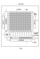
- 1 is a system configuration diagram illustrating a schematic configuration example of a light detection device according to each embodiment of the present disclosure.
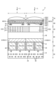
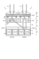
- 1 is a cross-sectional view illustrating a schematic structure of a pixel region according to a first embodiment of the present disclosure.
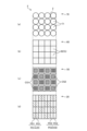
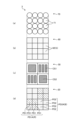
- 2A to 2C are diagrams for explaining a layered structure and a planar structure of a pixel region according to the first embodiment of the present disclosure.
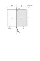
- 1A to 1C are diagrams for explaining the principle of a color splitter according to each embodiment of the present disclosure.
- 4A and 4B are diagrams illustrating an incident state of green light in a pixel region according to the first embodiment of the present disclosure.
- 4A and 4B are diagrams illustrating an incident state of red light in a pixel region according to the first embodiment of the present disclosure.
- 4A and 4B are diagrams illustrating an incident state of blue light in a pixel region according to the first embodiment of the present disclosure.
- 11A to 11C are diagrams for explaining a layered structure and a planar structure of a pixel region according to Modification 1 of the first embodiment of the present disclosure.
- 13A to 13C are diagrams for explaining a layered structure and a planar structure of a pixel region according to Modification 2 of the first embodiment of the present disclosure.
- 13A to 13C are diagrams for explaining a layered structure and a planar structure of a pixel region according to Modification 3 of the first embodiment of the present disclosure.
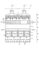
- FIG. 11 is a cross-sectional view illustrating a schematic structure of a pixel region according to a fourth modified example of the first embodiment of the present disclosure.
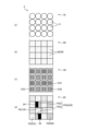
- 13A to 13C are diagrams for explaining a layered structure and a planar structure of a pixel region according to Modification 4 of the first embodiment of the present disclosure.
- 13A to 13C are diagrams for explaining a layered structure and a planar structure of a pixel region according to a fifth modified example of the first embodiment of the present disclosure.
- 13A to 13C are diagrams for explaining a layered structure and a planar structure of a pixel region according to a sixth modified example of the first embodiment of the present disclosure.
- FIGS. 13A to 13C are diagrams for explaining a layered structure and a planar structure of a pixel region according to Modification 7 of the first embodiment of the present disclosure.
- FIG. 11 is a cross-sectional view illustrating a schematic structure of a pixel region according to a second embodiment of the present disclosure.
- 13A and 13B are diagrams for explaining a layered structure and a planar structure of a pixel region according to a second embodiment of the present disclosure.
- 13A and 13B are diagrams for explaining a layered structure and a planar structure of a pixel region according to Modification 1 of the second embodiment of the present disclosure.
- FIG. 13A and 13B are diagrams for explaining a layered structure and a planar structure of a pixel region according to Modification 2 of the second embodiment of the present disclosure.
- 13A and 13B are diagrams for explaining a layered structure and a planar structure of a pixel region according to Modification 3 of the second embodiment of the present disclosure.
- FIG. 13 is a cross-sectional view illustrating a schematic structure of a pixel region according to Modification 4 of the second embodiment of the present disclosure.
- 13A and 13B are diagrams for explaining a layered structure and a planar structure of a pixel region according to Modification 4 of the second embodiment of the present disclosure.
- 13 is a cross-sectional view illustrating a schematic structure of a pixel region according to a fifth modified example of the second embodiment of the present disclosure.
- 13A and 13B are diagrams for explaining a layered structure and a planar structure of a pixel region according to a fifth modified example of the second embodiment of the present disclosure.
- 13A to 13C are diagrams for explaining a layered structure and a planar structure of a pixel region according to a sixth modified example of the second embodiment of the present disclosure.
- 13A to 13C are diagrams for explaining a layered structure and a planar structure of a pixel region according to a seventh modified example of the second embodiment of the present disclosure.
- FIG. 13A to 13C are diagrams for explaining a layered structure and a planar structure of a pixel region according to Modification 8 of the second embodiment of the present disclosure.
- FIG. 13 is a cross-sectional view illustrating a schematic structure of a pixel region according to a ninth modified example of the second embodiment of the present disclosure.
- 13A to 13C are diagrams for explaining a layered structure and a planar structure of a pixel region according to a ninth modified example of the second embodiment of the present disclosure.
- 13A to 13C are diagrams for explaining a layered structure and a planar structure of a pixel region according to a third embodiment of the present disclosure.
- FIG. 13A to 13C are diagrams for explaining a layered structure and a planar structure of a pixel region according to Modification 1 of the third embodiment of the present disclosure.
- 13A to 13C are diagrams for explaining a layered structure and a planar structure of a pixel region according to Modification 2 of the third embodiment of the present disclosure.
- FIG. 11 is a cross-sectional view illustrating a schematic structure of a pixel region according to a fourth embodiment of the present disclosure.
- 13A and 13B are diagrams for explaining a layered structure and a planar structure of a pixel region according to a fourth embodiment of the present disclosure.
- FIG. 1 is a block diagram showing an example of the configuration of an electronic device.
- FIG. 1 is a block diagram showing an example of a schematic configuration of a vehicle control system
- 4 is an explanatory diagram showing an example of the installation positions of an outside-vehicle information detection unit and an imaging unit
- FIG. 1 is a diagram illustrating an example of a schematic configuration of an endoscopic surgery system
- 2 is a block diagram showing an example of the functional configuration of a camera head and a CCU.
- stacked image sensors have been proposed in which multiple photoelectric conversion elements are stacked along the light incidence direction.
- a solid-state imaging element has been proposed in which a photoelectric conversion section that photoelectrically converts light in one wavelength range is provided on the light incidence side, and a photoelectric conversion section that photoelectrically converts light in a different wavelength range is provided on the opposite side to the light incidence side.
- FIG. 1 is a diagram showing a configuration example of a photodetection device 1 according to each embodiment of the present disclosure.
- the photodetection device 1 of this example is configured to have a pixel region 3 and a peripheral circuit unit.
- the pixel region 3 is a so-called imaging region in which pixels 2, each including a plurality of photoelectric conversion elements, are regularly and two-dimensionally arranged on a semiconductor substrate 11, for example, a silicon substrate.
- the pixel 2 includes a photoelectric conversion element, such as a photodiode, and a number of pixel transistors (so-called MOS transistors).
- the pixel transistors can be composed of three transistors, for example: a transfer transistor (a charge transfer section, described later), a reset transistor, and an amplification transistor.
- the multiple pixel transistors can also be configured with four transistors by adding a selection transistor.
- Pixel 2 can also have a shared pixel structure.
- This pixel sharing structure is configured with multiple photodiodes, multiple transfer transistors, one shared floating diffusion region, and one shared other pixel transistor each.
- the peripheral circuit section is composed of a vertical drive circuit 4, a column signal processing circuit 5, a horizontal drive circuit 6, an output circuit 7, and a control circuit 8.
- the control circuit 8 receives an input clock and data that commands the operating mode, etc., and also outputs data such as internal information of the photodetector 1.
- control circuit 8 generates clock signals and control signals that serve as the basis for the operation of the vertical drive circuit 4, column signal processing circuit 5, horizontal drive circuit 6, etc., based on the vertical synchronization signal, horizontal synchronization signal, and master clock. These signals are then input to the vertical drive circuit 4, column signal processing circuit 5, horizontal drive circuit 6, etc.
- the vertical drive circuit 4 is configured, for example, by a shift register, and selects pixel drive wiring 13, supplies a pulse to the selected pixel drive wiring to drive the pixels, and drives the pixels row by row.
- the vertical drive circuit 4 selects and scans each pixel 2 in the pixel region 3 in the vertical direction in a row-by-row sequence.
- the vertical drive circuit 4 then supplies a pixel signal based on a signal charge generated in response to the amount of light received in, for example, a photodiode that serves as a photoelectric conversion element in each pixel 2 to the column signal processing circuit 5 via a vertical signal line 9.
- the column signal processing circuit 5 is arranged, for example, for each column of pixels 2, and performs signal processing such as noise removal on the signals output from one row of pixels 2 for each pixel column.
- the column signal processing circuit 5 performs signal processing such as CDS (Correlated Double Sampling) for removing fixed pattern noise specific to the pixel 2, signal amplification, and AD conversion.
- a horizontal selection switch (not shown) is provided at the output stage of the column signal processing circuit 5 and connected between the output stage and the horizontal signal line 10.
- the horizontal drive circuit 6 is, for example, configured with a shift register, and by sequentially outputting horizontal scanning pulses, selects each of the column signal processing circuits 5 in turn, and causes each of the column signal processing circuits 5 to output a pixel signal to the horizontal signal line 10.
- the output circuit 7 processes and outputs the signals sequentially supplied from each of the column signal processing circuits 5 through the horizontal signal line 10. In this signal processing, for example, only buffering may be performed, or black level adjustment, column variation correction, various digital signal processing, etc. may be performed.
- the input/output terminal 12 exchanges signals with the outside.
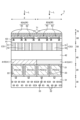
- Fig. 2 is a cross-sectional view that illustrates a schematic structure of the pixel region 3 according to the first embodiment of the present disclosure
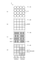
- Fig. 3 is a view for illustrating the layered structure and planar structure of the pixel region 3 according to the first embodiment of the present disclosure.
- FIG. 3 and subsequent drawings similar to FIG. 3 the photoelectric conversion units and photodiodes that receive light in the same wavelength range are hatched in the same manner to facilitate understanding.
- the photoelectric conversion units and photodiodes are arranged in order from the side where external incident light L is incident (hereinafter also referred to as the light incident side or directly above), as (a), (b), (c), and (d).
- the pixel region 3 includes a semiconductor layer 20, a wiring layer 30, an optical layer 40, a color splitter layer 50, an organic photoelectric conversion layer 60, and an OCL (on-chip lens) layer 70.
- the semiconductor layer 20 is an example of a photoelectric conversion layer
- the organic photoelectric conversion layer 60 is an example of another photoelectric conversion layer.
- an OCL layer 70, an organic photoelectric conversion layer 60, a color splitter layer 50, an optical layer 40, a semiconductor layer 20 and a wiring layer 30 are stacked in this order from the light incident side.
- the semiconductor layer 20 has a semiconductor region 21 of a first conductivity type (e.g., P type), a semiconductor region 22 of a second conductivity type (e.g., N type), and a separation portion 23. Then, within the semiconductor region 21 of the first conductivity type, the semiconductor regions 22 of the second conductivity type are formed side by side in the planar direction (arrangement direction of the pixels 2) on a pixel-by-pixel basis, so that photodiodes PD1 and PD2 formed by PN junctions are formed side by side in the planar direction.
- a first conductivity type e.g., P type
- a semiconductor region 22 of a second conductivity type e.g., N type
- Photodiode PD1 is an example of a first photoelectric conversion unit
- photodiode PD2 is an example of a second photoelectric conversion unit.
- photodiode PD1 is a photoelectric conversion unit that receives light in the red wavelength range (hereinafter also referred to as the "red region") and performs photoelectric conversion.
- the red wavelength range (red region) is an example of a first wavelength range.
- the photodiode PD2 is a photoelectric conversion unit that receives light in the blue wavelength range (hereinafter also referred to as the "blue region") and performs photoelectric conversion.
- the blue wavelength range (blue region) is an example of a second wavelength range.
- a photodiode group PD1A is formed by two adjacent photodiodes PD1
- a photodiode group PD2A is formed by two adjacent photodiodes PD2.
- the photodiode groups PD1A and PD2A are examples of photoelectric conversion unit groups.
- a plurality of photodiode groups PD1A and a plurality of photodiode groups PD2A are arranged in a checkerboard pattern.
- the photodiode groups PD1A and the photodiode groups PD2A are formed individually for each pixel 2 (see FIG. 2) in the pixel region 3.
- the separation portions 23 of the semiconductor layer 20 electrically and optically separate the adjacent photodiodes PD1 from each other, the adjacent photodiodes PD1 and PD2 from each other, and the adjacent photodiodes PD2 from each other.
- photodiodes PD1 belonging to the same photodiode group PD1A may be electrically connected to each other via a same-color path (hereinafter also referred to as an overflow path) for discharging carriers to the other pixel when one of the photodiodes is saturated.
- photodiodes PD2 belonging to the same photodiode group PD2A may be electrically connected to each other via an overflow path.
- the isolation portion 23 is made of a material such as an oxide film or a metal film, for example, a silicon oxide film, a silicon nitride film, amorphous silicon, polycrystalline silicon, a titanium oxide film, aluminum, or tungsten.
- a wiring layer 30 is disposed on the surface of the semiconductor layer 20 opposite the light incident side (hereinafter also referred to as the back side or directly below).
- the wiring layer 30 is configured by forming a plurality of wiring films 32 and a plurality of pixel transistors 33 within an interlayer insulating film 31.
- the plurality of pixel transistors 33 perform functions such as reading out the charges accumulated in the photodiodes PD1 and PD2 and the photoelectric conversion unit 62 described below.
- An optical layer 40 is disposed on the light-incident surface of the semiconductor layer 20.
- the optical layer 40 has a color filter 41 and a buffer layer 42.
- the color filter 41 and the buffer layer 42 are stacked in this order from the light-incident side.
- the color filter 41 is an optical filter that transmits light of a specific wavelength range from the incident light L.
- the color filter 41 includes, for example, a color filter 41R that transmits light in the red region and a color filter 41B that transmits light in the blue region.
- Color filter 41R is disposed on the light incident side of photodiode group PD1A (see FIG. 3).
- Color filter 41B is disposed on the light incident side of photodiode group PD2A (see FIG. 3).
- Color filter 41R or color filter 41B is formed, for example, individually for each pixel 2 in pixel region 3.
- a planarization layer (not shown) may be provided between the semiconductor layer 20 and the color filter 41 to planarize the surface on which the color filter 41 is formed and to avoid unevenness that occurs during the spin coating process when forming the color filter 41.
- the buffer layer 42 is provided to adjust the focal length of the color splitters CS1 and CS2 located in the color splitter layer 50 described below.
- the buffer layer 42 is made of, for example, silicon oxide, and has a thickness of about 1 ( ⁇ m) to 3 ( ⁇ m).
- a color splitter layer 50 is disposed on the light-incident surface of the optical layer 40.
- the color splitter layer 50 has a low refractive index portion 51 and high refractive index portions 52 and 53.
- the low refractive index portion 51 is made of a material having a lower refractive index than the high refractive index portions 52 and 53.
- the low refractive index portion 51 is made of, for example, a metal oxide such as silicon oxide or aluminum oxide, or an organic material such as an acrylic resin.
- the high refractive index portions 52 and 53 are made of a material having a higher refractive index than the low refractive index portion 51.
- the high refractive index portions 52 and 53 are made of, for example, silicon compounds such as silicon nitride and silicon carbide, metal oxides such as titanium oxide, tantalum oxide, niobium oxide, hafnium oxide, indium oxide, and tin oxide, or composite oxides of these.
- the high refractive index portions 52 and 53 may also be made of an organic material such as siloxane.
- the high refractive index section 52 has a predetermined planar shape inside the color splitter layer 50, and is disposed on the light incident side of the photodiode group PD1A.
- the low refractive index section 51 and the high refractive index section 52 form the color splitter CS1 on the light incident side of the photodiode group PD1A.
- the high refractive index section 53 has a predetermined planar shape inside the color splitter layer 50, and is disposed on the light incident side of the photodiode group PD2A.
- the low refractive index section 51 and the high refractive index section 53 form the color splitter CS2 on the light incident side of the photodiode group PD2A.
- multiple color splitters CS1 and multiple color splitters CS2 are arranged in a checkerboard pattern.
- Color splitter CS1 or color splitter CS2 is formed, for example, individually for each pixel 2 (see FIG. 2) in pixel area 3. The function of these color splitters CS1 and CS2 will be described later.
- an organic photoelectric conversion layer 60 is disposed on the light incident surface of the color splitter layer 50.
- the organic photoelectric conversion layer 60 has an interlayer insulating film 61 and a photoelectric conversion section 62.
- the photoelectric conversion section 62 is an example of another photoelectric conversion section.
- the photoelectric conversion section 62 and the interlayer insulating film 61 are stacked in this order from the light incident side.
- the interlayer insulating film 61 is composed of, for example, a single layer film made of one of silicon oxide, TEOS, silicon nitride, silicon oxynitride, etc., or a laminate film made of two or more of these.
- the photoelectric conversion section 62 has an upper electrode 62a, a photoelectric conversion layer 62b, a charge storage layer 62c, lower electrodes 62d, 62e, and an insulating layer 62f.
- the upper electrode 62a, the photoelectric conversion layer 62b, the charge storage layer 62c, the insulating layer 62f, and the lower electrodes 62d, 62e are stacked in this order from the light incident side.
- the upper electrode 62a, photoelectric conversion layer 62b, charge storage layer 62c and insulating layer 62f are formed, for example, in common to all pixels 2 in the pixel region 3, and the lower electrodes 62d and 62e are formed, for example, separately for each pixel 2 in the pixel region 3. That is, the photoelectric conversion section 62 is formed, for example, individually for each pixel 2 (see FIG. 2) in the pixel region 3, as shown in FIG. 3(b).
- the upper electrode 62a is electrically connected to the wiring film 32 of the wiring layer 30 via a wiring layer or a through electrode (neither of which are shown) at the periphery of the pixel region 3.
- the upper electrode 62a is made of a transparent conductive material such as indium tin oxide (ITO).
- the material of the upper electrode 62a and the lower electrode 62d is not limited to ITO, and various transparent conductive materials (for example, tin oxide, zinc oxide, IZO, IGO, IGZO, ATO, AZO) can be used.
- IZO is an oxide in which indium is added to zinc oxide
- IGO is an oxide in which indium is added to gallium oxide
- IGZO is an oxide in which indium and gallium are added to zinc oxide
- ATO is an oxide in which antimony is added to tin oxide
- AZO is an oxide in which antimony is added to zinc oxide.
- the photoelectric conversion layer 62b is made of an organic semiconductor material and photoelectrically converts light in a selective wavelength range (for example, the green wavelength range (hereinafter also referred to as the "green region")) of the incident light L from the outside.
- the green wavelength range (green region) is an example of a third wavelength range.
- the photoelectric conversion layer 62b preferably contains one or both of a p-type organic semiconductor and an n-type organic semiconductor.
- the photoelectric conversion layer 62b is preferably composed of, for example, quinacridone, quinacridone derivatives, subphthalocyanine, and subphthalocyanine derivatives, and preferably contains at least one of these materials.
- the photoelectric conversion layer 62b is not limited to such materials, and may be, for example, at least one of naphthalene, anthracene, phenanthrene, tetracene, pyrene, perylene, and fluoranthene (all of which include derivatives).
- the photoelectric conversion layer 62b may also contain polymers or derivatives of phenylenevinylene, fluorene, carbazole, indole, pyrene, pyrrole, picoline, thiophene, acetylene, diacetylene, and the like.
- the photoelectric conversion layer 62b may also contain metal complex dyes, cyanine dyes, merocyanine dyes, phenylxanthene dyes, triphenylmethane dyes, rhodacyanine dyes, xanthene dyes, etc.
- the photoelectric conversion layer 62b may contain other organic materials such as fullerene (C 60 ) and BCP (Bathocuproine).
- photoelectric conversion layer 62b When photoelectric conversion of green light is performed in the photoelectric conversion layer 62b, for example, rhodamine-based dyes, melacyanine-based dyes, quinacridone derivatives, subphthalocyanine-based dyes (subphthalocyanine derivatives), etc. can be used in the photoelectric conversion layer 62b.
- the charge storage layer 62c is provided between the photoelectric conversion layer 62b and the insulating layer 62f, and stores the charge generated in the photoelectric conversion layer 62b.
- the charge storage layer 62c is preferably formed using a material that has a higher charge mobility and a larger band gap than the photoelectric conversion layer 62b.
- the band gap of the material constituting the charge storage layer 62c is preferably 3.0 eV or more.
- examples of such materials include oxide semiconductor materials such as IGZO and organic semiconductor materials.
- organic semiconductor materials include transition metal dichalcogenides, monovalent silicon (SiC), diamond, graphene, carbon nanotubes, condensed polycyclic hydrocarbon compounds, and condensed heterocyclic compounds.
- the lower electrodes 62d and 62e are made of the same material as the upper electrode 62a (e.g., ITO, etc.).
- the lower electrode 62d is electrically connected to the charge storage layer 62c and is also electrically connected to metal wiring (not shown) that penetrates the interlayer insulating film 61, the color splitter layer 50, the optical layer 40, and the semiconductor layer 20.
- These metal wiring lines are made of materials such as tungsten (W), titanium (Ti), aluminum (Al), and copper (Cu). These metal wiring lines also function as light-shielding films between pixels.
- this metal wiring is electrically connected to a charge storage section (not shown) formed near the interface on the side opposite to the light incident side of the semiconductor region 21.
- a charge storage section is formed in a semiconductor region of the second conductivity type (for example, N type).
- the lower electrode 62e is electrically connected to the wiring film 32 of the wiring layer 30 via a wiring film 63 formed in the interlayer insulating film 61 and a through electrode (not shown).
- the electric charge generated by photoelectric conversion in the photoelectric conversion unit 62 is transferred to the charge storage unit via metal wiring.
- the charge storage unit temporarily stores the electric charge photoelectrically converted in the photoelectric conversion unit 62 until it is read out by the corresponding pixel transistor 33.
- a predetermined voltage is applied to the lower electrodes 62d, 62e and the upper electrode 62a from a drive circuit (not shown).
- a positive voltage is applied to the lower electrodes 62d, 62e, and a negative voltage is applied to the upper electrode 62a.
- a larger positive voltage is applied to the lower electrode 62e than to the lower electrode 62d.
- a reset operation is performed by operating a reset transistor (not shown) in the latter part of the charge storage period. This resets the potential of the charge storage section, and the potential of the charge storage section becomes the power supply voltage.
- pixel 2 After the reset operation is completed, pixel 2 performs a charge transfer operation. In this charge transfer operation, a positive voltage higher than that of lower electrode 62e is applied to lower electrode 62d from the drive circuit. As a result, the electrons stored in charge storage layer 62c are transferred to the charge storage section via lower electrode 62d and metal wiring (not shown).
- the OCL layer 70 has a plurality of OCLs 71.
- the OCLs 71 are formed in a hemispherical shape, and are provided for each pixel 2 (see FIG. 2) in the pixel region 3, as shown in FIG. 3(a), for example, and are lenses that focus the incident light L on the photoelectric conversion unit 62, photodiode PD1, and photodiode PD2 of each pixel 2.
- the OCLs 71 are made of, for example, an acrylic resin.
- FIG. 4 is a diagram for explaining the principle of the color splitters CS1 and CS2 according to each embodiment of the present disclosure.
- the color splitter CS1 (or color splitter CS2) has a first region R1 in which the low refractive index section 51 is located, and a second region R2 in which the high refractive index sections 52 and 53 are located.
- a low refractive index portion 51 having a low refractive index (e.g., a refractive index nR1 ) is arranged along the light incidence direction by a length X.
- high refractive index portions 52 and 53 having a high refractive index (e.g., a refractive index nR2 ) are arranged along the light incidence direction by a length X.
- a color splitter CS1 having such a configuration, when incident light L is incident on the first region R1 and the second region R2 simultaneously, the difference in refractive index between the low refractive index section 51 and the high refractive index sections 52 and 53 creates a difference in the distance traveled by the incident light L between the first region R1 and the second region R2.
- optical path length D1 of the first region R1 is calculated by the following formula (1).
- D1 n R1 ⁇ X...(1)
- the optical path length D2 of the second region R2 is calculated by the following formula (2).
- D2 n R2 ⁇ X...(2)
- the optical path difference ⁇ D between the first region R1 and the second region R2 is calculated by the following formula (3).
- the incident light L that passes through the color splitters CS1 and CS2 is bent and emitted toward the first region R1, where the light travels with a delay, due to the optical path length difference ⁇ D between the first region R1 and the second region R2, as shown in Figure 4.
- the bending angle ⁇ of the incident light L is calculated by the following formula (4).
- ⁇ wavelength of incident light L
- the bending angle ⁇ of the incident light L depends on the wavelength ⁇ of the incident light L. Therefore, by appropriately selecting the refractive indexes nR1 and nR2 of the low refractive index portion 51 and the high refractive index portion 52 in accordance with the respective wavelength ranges, the color splitters CS1 and CS2 can bend the light in the respective wavelength ranges in different desired directions.
- FIG. 5 is a diagram showing an incidence state of green light L 2 G in the pixel region 3 according to the first embodiment of the present disclosure. As shown in Fig. 5, green light L 2 G in the green wavelength range is absorbed by the photoelectric conversion unit 62 located closest to the light incidence side among the multiple photoelectric conversion units, and is photoelectrically converted by the photoelectric conversion unit 62.
- the OCL 71 allows the focused green light LG to be incident on the corresponding photoelectric conversion unit 62, thereby improving the sensitivity of the photoelectric conversion unit 62.
- red light L 1 R in the red wavelength range is partially absorbed by the photoelectric conversion unit 62 located closest to the light incidence side among the multiple photoelectric conversion units, and the rest is transmitted. Then, the red light L 1 R transmitted through the photoelectric conversion unit 62 reaches the color splitters CS1 and CS2 in the color splitter layer 50.
- the color splitter CS1 causes the red light L 1 R to be incident on the adjacent (i.e., directly below) photodiode group PD1A as shown in Fig. 6.
- the bending angle ⁇ is controlled so that the incident red light L 1 R is directed toward the photodiode group PD1A directly below.
- the color splitter CS2 causes the red light L 1 R to be incident on the adjacent photodiode group PD1A (i.e., adjacent to the photodiode group PD2A directly below it).
- the bending angle ⁇ is controlled so that the incident red light L 1 R is directed toward the adjacent photodiode group PD1A.
- the red light L 1 R incident on the adjacent OCL 71 can also be made to enter the photodiode group PD1A.
- focused red light L R is incident on the photodiode group PD1A from a color splitter area constituted by the color splitter CS1 directly above and a plurality of color splitters CS2 adjacent to the color splitter CS1 directly above.
- the sensitivity of the photodiode group PD1A that photoelectrically converts the red light L- R can be improved.
- FIG. 7 is a diagram showing an incidence state of blue light L 1 B in the pixel region 3 according to the first embodiment of the present disclosure.
- blue light L 1 B in the blue wavelength range is partially absorbed by the photoelectric conversion unit 62 located closest to the light incidence side among the multiple photoelectric conversion units, and the rest is transmitted. Then, the blue light L 1 B transmitted through the photoelectric conversion unit 62 reaches the color splitters CS1 and CS2 in the color splitter layer 50.
- the color splitter CS2 causes the blue light LB to be incident on the adjacent (i.e., directly below) photodiode group PD2A as shown in Fig. 7.
- the bending angle ⁇ is controlled so that the incident blue light LB is directed toward the photodiode group PD2A directly below.
- the color splitter CS1 causes the blue light LB to be incident on the adjacent photodiode group PD2A (i.e., adjacent to the photodiode group PD1A directly below it).
- the bending angle ⁇ is controlled so that the incident blue light LB is directed toward the adjacent photodiode group PD2A.
- the blue light L 1 B incident on the adjacent OCL 71 can also be made incident on the photodiode group PD2A.
- focused blue light LB is incident on the photodiode group PD2A from a color splitter area constituted by the color splitter CS2 directly above and a plurality of color splitters CS1 adjacent to the color splitter CS2 directly above.
- the sensitivity of the photodiode group PD2A that photoelectrically converts the blue light L 2 B can be improved.
- the sensitivity of the photodiode groups PD1A and PD2A can be improved by arranging the color splitters CS1 and CS2 closer to the light incident side than the photodiode groups PD1A and PD2A.
- two photodiodes PD1 belonging to the same photodiode group PD1A are configured as photoelectric conversion units capable of acquiring the phase difference on the image surface.
- two photodiodes PD1 belonging to the same photodiode group PD1A share the same range of color splitter area, which is composed of the color splitter CS1 directly above and multiple color splitters CS2 adjacent to that color splitter CS1.
- red light L and R incident on two photodiodes PD1 belonging to the same photodiode group PD1A is photoelectrically converted in each photodiode PD1 to generate electrons that become readout charges.
- the generated electrons are sequentially transferred to the floating diffusion region of the pixel circuit via the transfer transistor, and are read out as pixel signals for each photodiode PD1.
- the column signal processing circuit 5 receives the read-out pixel signals, detects the phase difference by comparing the signal amounts of each photodiode PD1, and calculates the distance to the object based on the detected phase difference.
- the red light L 1 R focused by the color splitter layer 50 is incident on the photodiode group PD1A, so that the detection sensitivity of the phase difference in the red light L 1 R can be improved.
- two photodiodes PD2 belonging to the same photodiode group PD2A are configured as photoelectric conversion units capable of acquiring the phase difference on the image surface.
- two photodiodes PD2 belonging to the same photodiode group PD2A share the same range of color splitter area, which is composed of the color splitter CS2 directly above and multiple color splitters CS1 adjacent to that color splitter CS2.
- blue light LB incident on two photodiodes PD2 belonging to the same photodiode group PD2A is photoelectrically converted in each photodiode PD2 to generate electrons that become readout charges.
- the generated electrons are sequentially transferred to the floating diffusion region of the pixel circuit via the transfer transistor, and are read out as pixel signals for each photodiode PD2.
- the column signal processing circuit 5 receives the read-out pixel signals, detects the phase difference by comparing the signal amounts of each photodiode PD2, and calculates the distance to the object based on the detected phase difference.
- the blue light L 1 B focused by the color splitter layer 50 is incident on the photodiode group PD2A, so that the detection sensitivity of the phase difference in the blue light L 1 B can be improved.
- the color splitters CS1 and CS2 have a metasurface structure.
- a metasurface structure is a structure in which the high refractive index sections 52 and 53 formed in one color splitter CS1 and CS2 are arranged at a period equal to or less than the wavelength ⁇ of the incident light L.
- the first embodiment it is possible to improve the sensitivity of the photodiode groups PD1A and PD2A that respectively photoelectrically convert the red light L R and the blue light L B. Furthermore, in the first embodiment, it is possible to improve the detection sensitivity of the phase difference in the red light L R and the blue light L B.
- a color filter 41R may be disposed between the color splitter CS1 and the photodiode group PD1A, and a color filter 41B may be disposed between the color splitter CS2 and the photodiode group PD2A.
- the photoelectric conversion unit 62 on the light incident side photoelectrically converts light in the green region
- the photodiode groups PD1A and PD2A on the opposite side to the light incident side photoelectrically convert light in the red region and blue region.
- the first embodiment it is possible to suppress the occurrence of color mixing in the photodiode groups PD1A and PD2A. Note that in the present disclosure, it is not necessarily required that the color filter 41 is provided in the optical layer 40.
- a buffer layer 42 may be provided in the optical layer 40. This allows the red light L R or the blue light L B to be efficiently incident on the desired photodiode group PD1A or PD2A even if the bending angle ⁇ of the color splitters CS1 and CS2 is made smaller.
- the buffer layer 42 is provided in the optical layer 40, so that more focused red light L R or blue light L B can be incident on the desired photodiode group PD1A or photodiode group PD2A. Therefore, according to the first embodiment, the detection sensitivity of the phase difference in the red light L R or blue light L B can be further improved.
- the organic photoelectric conversion layer 60 may be disposed on the light incident side of the color splitter layer 50. This allows the incident light L reaching the color splitters CS1 and CS2 to be split in advance by the photoelectric conversion unit 62 into light with a longer wavelength than the green region (i.e., red light L R ) and light with a shorter wavelength than the green region (i.e., blue light L B ).
- the first embodiment it is possible to suppress the occurrence of color mixing in the photodiode groups PD1A and PD2A.
- light in the red region may be photoelectrically converted in the photoelectric conversion section 62 on the light incident side
- light in the green region and light in the blue region may be photoelectrically converted in the semiconductor layer 20 on the rear side.
- light in the blue region may be photoelectrically converted in the photoelectric conversion section 62 on the light incident side
- light in the red region and light in the green region may be photoelectrically converted in the semiconductor layer 20 on the rear side.
- Fig. 8 is a diagram for explaining the layered structure and planar structure of the pixel region 3 according to Modification 1 of the first embodiment of the present disclosure, and corresponds to Fig. 3 of the first embodiment.
- the configuration of the semiconductor layer 20 differs from that of the first embodiment (see FIG. 3) described above. Specifically, in this modified example 1, the photodiode groups PD1A, PD2A are not provided in the majority of the pixels 2 (see FIG. 2), and one photodiode PD1 or one photodiode PD2 is provided in the majority of the pixels 2.
- some of the pixels 2 are provided with a photodiode PD2 whose light receiving area is halved by a light shielding film 24 located on one side (e.g., the left side).
- another portion of adjacent pixels 2 are provided with a photodiode PD2 whose light receiving area is halved by a light shielding film 24 located on the other side (e.g., the right side).
- the two photodiodes PD2 with their areas halved, form one photodiode group PD2A.
- the two photodiodes PD2 belonging to the same photodiode group PD2A are configured as a photoelectric conversion unit capable of acquiring the phase difference of the image plane.
- one photodiode group PD2A is formed by two photodiodes PD2 each having half the light receiving area, but the present disclosure is not limited to such an example.
- one photodiode group PD1A may be configured by two photodiodes PD1 with half the light receiving area, and the two photodiodes PD1 may be configured as a photoelectric conversion unit capable of acquiring the phase difference on the image plane, thereby improving the detection sensitivity of the phase difference in the red light L R (see FIG. 6).
- FIG. 9 is a diagram for explaining the layered structure and planar structure of the pixel region 3 according to the second modification of the first embodiment of the present disclosure. As shown in FIG. 9, in the second modification, the configurations of the color splitter layer 50 and the semiconductor layer 20 differ from those in the first embodiment described above (see FIG. 3).
- color splitters CS1 and CS2 each having an area equivalent to 2 x 2 OCL71, are provided in the color splitter layer 50.
- These four photodiodes PD1 form one photodiode group PD1A. Furthermore, in this modification 2, the four photodiodes PD1 belonging to the same photodiode group PD1A are configured as a photoelectric conversion unit capable of acquiring the phase difference of the image plane.
- the four photodiodes PD1 belonging to the same photodiode group PD1A share the same range of color splitter area, which is composed of the color splitter CS1 directly above and multiple color splitters CS2 adjacent to this color splitter CS1.
- the red light L R (see FIG. 6) focused by the color splitter layer 50 is incident on the photodiode group PD1A, so that the detection sensitivity of the phase difference in the red light L R can be improved.
- These four photodiodes PD2 form one photodiode group PD2A. Furthermore, in this modification 2, the four photodiodes PD2 belonging to the same photodiode group PD2A are configured as a photoelectric conversion unit capable of acquiring the phase difference of the image plane.
- the four photodiodes PD2 belonging to the same photodiode group PD2A share the same range of color splitter area, which is composed of the color splitter CS2 directly above and the multiple color splitters CS1 adjacent to that color splitter CS2.
- the blue light L B (see FIG. 7) focused by the color splitter layer 50 is incident on the photodiode group PD2A, so that the detection sensitivity of the phase difference in the blue light L B can be improved.
- the photodiode groups PD1A and PD2A each have 2 x 2 photodiodes PD1 and PD2, so the distance to the object can be measured regardless of the texture direction or the color of the object.
- FIG. 10 is a diagram for explaining the layered structure and planar structure of the pixel region 3 according to the third modification of the first embodiment of the present disclosure. As shown in FIG. 10, in the third modification, the configurations of the color splitter layer 50 and the semiconductor layer 20 differ from those in the first embodiment described above (see FIG. 3).
- color splitters CS1 and CS2 having an area of 2 x 1 OCL71 are provided in the color splitter layer 50.
- two photodiodes PD1 (2 x 1) are located behind the color splitter CS1.
- the two photodiodes PD1 form one photodiode group PD1A. Furthermore, in this modification example 3, the two photodiodes PD1 belonging to the same photodiode group PD1A are configured as a photoelectric conversion unit capable of acquiring the phase difference of the image surface.
- two photodiodes PD1 belonging to the same photodiode group PD1A share the same range of color splitter area, which is composed of the color splitter CS1 directly above and multiple color splitters CS2 adjacent to that color splitter CS1.
- the red light L R (see FIG. 6) focused by the color splitter layer 50 is incident on the photodiode group PD1A, so that the detection sensitivity of the phase difference in the red light L R can be improved.
- two photodiodes PD2 are located on the rear side of the color splitter CS2.
- the two photodiodes PD2 form one photodiode group PD2A. Furthermore, in this modification example 3, the two photodiodes PD2 belonging to the same photodiode group PD2A are configured as a photoelectric conversion unit capable of acquiring the phase difference of the image surface.
- two photodiodes PD2 belonging to the same photodiode group PD2A share the same range of color splitter area, which is composed of the color splitter CS2 directly above and multiple color splitters CS1 adjacent to that color splitter CS2.
- the blue light L B (see FIG. 7) focused by the color splitter layer 50 is incident on the photodiode group PD2A, so that the detection sensitivity of the phase difference in the blue light L B can be improved.
- FIG. 11 is a cross-sectional view that shows a schematic structure of pixel region 3 according to modification 4 of the first embodiment of the present disclosure
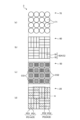
- FIG. 12 is a diagram for explaining the layered structure and planar structure of pixel region 3 according to modification 4 of the first embodiment of the present disclosure.
- the configuration of the organic photoelectric conversion layer 60 differs from that of the first embodiment described above (see Figures 2 and 3). Specifically, in this modification 4, two photoelectric conversion units 62 are located at the back side of one OCL 71, and these two photoelectric conversion units 62 form one photoelectric conversion unit group 62A.
- the photoelectric conversion unit group 62A is an example of another photoelectric conversion unit group.
- two photoelectric conversion units 62 belonging to the same photoelectric conversion unit group 62A are configured as photoelectric conversion units capable of acquiring the phase difference of the image plane.
- the two photoelectric conversion units 62 belonging to the same photoelectric conversion unit group 62A share the OCL 71 directly above.
- the green light L G (see FIG. 5) focused by the OCL 71 is incident on the photoelectric conversion unit group 62A, so that the detection sensitivity of the phase difference in the green light L G can be improved.
- the OCL 71 and the color splitter layer 50 can focus all three colors of RGB light, improving the detection sensitivity of the phase difference in all three colors of RGB light.
- the color splitter layer 50 and the semiconductor layer 20 have the same configuration as in the first embodiment (see FIG. 3) described above, but the present disclosure is not limited to such an example.
- the semiconductor layer 20 may have the same configuration as in the above-mentioned modified example 1 (see FIG. 8).
- the color splitter layer 50 and the semiconductor layer 20 may have the same configuration as in the above-mentioned modification 2 (see FIG. 9), or the color splitter layer 50 and the semiconductor layer 20 may have the same configuration as in the above-mentioned modification 3 (see FIG. 10).
- FIG. 13 is a diagram for explaining the layered structure and planar structure of the pixel region 3 according to the fifth modification of the first embodiment of the present disclosure. As shown in FIG. 13, in the fifth modification, the configuration of the organic photoelectric conversion layer 60 differs from that in the fourth modification of the first embodiment described above (see FIG. 12).
- the photoelectric conversion unit group 62A is not provided in the majority of the pixels 2, and one photoelectric conversion unit 62 is provided in the majority of the pixels 2.
- pixels 2 are provided with photoelectric conversion units 62 whose light receiving area is halved by a light shielding film 64 located on one side (e.g., the left side).
- another set of adjacent pixels 2 are provided with photoelectric conversion units 62 whose light receiving area is halved by a light shielding film 64 located on the other side (e.g., the right side).
- the two photoelectric conversion units 62 with their surface area halved, form one photoelectric conversion unit group 62A. Furthermore, in this variant example 5, the two photoelectric conversion units 62 belonging to the same photoelectric conversion unit group 62A are configured as photoelectric conversion units capable of acquiring the phase difference of the image plane.
- the green light L G (see FIG. 5) focused by the OCL 71 is incident on the photoelectric conversion unit group 62A, so that the detection sensitivity of the phase difference in the green light L G can be improved.
- the OCL 71 and the color splitter layer 50 can focus all three colors of RGB light, respectively, improving the detection sensitivity of the phase difference in all three colors of RGB light.
- the color splitter layer 50 and the semiconductor layer 20 have the same configuration as in the first embodiment (see FIG. 3) described above, but the present disclosure is not limited to such an example.
- the semiconductor layer 20 may have the same configuration as in the above-mentioned modified example 1 (see FIG. 8).
- the color splitter layer 50 and the semiconductor layer 20 may have the same configuration as in the above-mentioned modification 2 (see FIG. 9), or the color splitter layer 50 and the semiconductor layer 20 may have the same configuration as in the above-mentioned modification 3 (see FIG. 10).
- FIG. 14 is a diagram for explaining the layered structure and planar structure of the pixel region 3 according to the sixth modification of the first embodiment of the present disclosure. As shown in FIG. 14, in the sixth modification, the configuration of the OCL layer 70 and the organic photoelectric conversion layer 60 differs from that in the fourth modification of the first embodiment described above (see FIG. 12).
- a plurality of OCLs 71A each having an area equivalent to 2 x 2 pixels 2 (see FIG. 11) are arranged in a matrix on the OCL layer 70.
- 2 x 2 photoelectric conversion units 62, totaling four, are located behind each OCL 71A.
- These four photoelectric conversion units 62 form one photoelectric conversion unit group 62A. Furthermore, in this modification 6, the four photoelectric conversion units 62 belonging to the same photoelectric conversion unit group 62A are configured as photoelectric conversion units capable of acquiring the phase difference of the image plane. In this case, the four photoelectric conversion units 62 belonging to the same photoelectric conversion unit group 62A share the OCL 71A directly above them.
- the green light L G (see FIG. 5) focused by the OCL 71A is incident on the photoelectric conversion unit group 62A, so that the detection sensitivity of the phase difference in the green light L G can be improved.
- the OCL 71A and the color splitter layer 50 can focus all three colors of RGB light, improving the detection sensitivity of the phase difference in all three colors of RGB light.
- the photoelectric conversion unit group 62A has 2 x 2 photoelectric conversion units 62, so the distance to the target object can be measured regardless of the texture direction.
- the color splitter layer 50 and the semiconductor layer 20 have the same configuration as in the first embodiment (see FIG. 3) described above, but the present disclosure is not limited to such an example.
- the semiconductor layer 20 may have the same configuration as in the above-mentioned modified example 1 (see FIG. 8).
- the color splitter layer 50 and the semiconductor layer 20 may have the same configuration as in the above-mentioned modification 2 (see FIG. 9), or the color splitter layer 50 and the semiconductor layer 20 may have the same configuration as in the above-mentioned modification 3 (see FIG. 10).
- FIG. 15 is a diagram for explaining the layered structure and planar structure of the pixel region 3 according to the seventh modification of the first embodiment of the present disclosure. As shown in FIG. 15, in the seventh modification, the configuration of the OCL layer 70 differs from that of the first embodiment described above (see FIG. 3).
- a semi-elliptical spherical OCL 71B having an area equivalent to 2 ⁇ 1 pixels 2 (see FIG. 11) is provided in a part of the OCL layer 70.
- two photoelectric conversion units 62 (2 ⁇ 1) are located behind the OCL 71B.
- These two photoelectric conversion units 62 form one photoelectric conversion unit group 62A. Furthermore, in this modification example 7, the two photoelectric conversion units 62 belonging to the same photoelectric conversion unit group 62A are configured as photoelectric conversion units capable of acquiring the phase difference of the image plane. In this case, the two photoelectric conversion units 62 belonging to the same photoelectric conversion unit group 62A share the OCL 71B directly above them.
- the green light L G (see FIG. 5) focused by the OCL 71B is incident on the photoelectric conversion unit group 62A, so that the detection sensitivity of the phase difference in the green light L G can be improved.
- the OCL 71B and the color splitter layer 50 can focus all three colors of RGB light, improving the detection sensitivity of the phase difference in all three colors of RGB light.
- the color splitter layer 50 and the semiconductor layer 20 have the same configuration as in the first embodiment (see FIG. 3) described above, but the present disclosure is not limited to such an example.
- the semiconductor layer 20 may have the same configuration as in the above-mentioned modified example 1 (see FIG. 8).
- the color splitter layer 50 and the semiconductor layer 20 may have the same configuration as in the above-mentioned modification 2 (see FIG. 9), or the color splitter layer 50 and the semiconductor layer 20 may have the same configuration as in the above-mentioned modification 3 (see FIG. 10).
- Fig. 16 is a cross-sectional view that illustrates a schematic structure of the pixel region 3 according to the second embodiment of the present disclosure
- Fig. 17 is a view for illustrating a layered structure and a planar structure of the pixel region 3 according to the second embodiment of the present disclosure.
- the pixel region 3 of the second embodiment includes a semiconductor layer 20, a wiring layer 30, an optical layer 40, a color splitter layer 50, an organic photoelectric conversion layer 60, and an OCL layer 70.
- the OCL layer 70, the organic photoelectric conversion layer 60, the color splitter layer 50, the optical layer 40, the semiconductor layer 20, and the wiring layer 30 are stacked in this order from the light incident side.
- the semiconductor layer 20 has a semiconductor region 21 of a first conductivity type (e.g., P type), a semiconductor region 22 of a second conductivity type (e.g., N type), and an isolation section 23. Then, within the semiconductor region 21 of the first conductivity type, the semiconductor regions 22 of the second conductivity type are formed side by side in the planar direction (arrangement direction of the pixels 2) on a pixel-by-pixel basis, so that photodiodes PD1, PD2, and PD3 formed by PN junctions are formed side by side in the planar direction.
- the photodiode PD3 is an example of a third photoelectric conversion section.
- photodiode PD1 is a photoelectric conversion unit that receives light in the red region and performs photoelectric conversion.
- Photodiode PD2 is a photoelectric conversion unit that receives light in the blue region and performs photoelectric conversion.
- Photodiode PD3 is a photoelectric conversion unit that receives light in the green region and performs photoelectric conversion. That is, in this second embodiment, the semiconductor layer 20 photoelectrically converts each of the three colors of RGB light.
- a photodiode group PD1A is formed by two adjacent photodiodes PD1.
- a photodiode group PD2A is formed by two adjacent photodiodes PD2, and a photodiode group PD3A is formed by two adjacent photodiodes PD3.
- the photodiode group PD3A is an example of a photoelectric conversion unit group.
- a plurality of photodiode groups PD1A, a plurality of photodiode groups PD2A, and a plurality of photodiode groups PD3A are arranged in a so-called Bayer array.
- the photodiode groups PD1A, PD2A, and PD3A are formed individually for each pixel 2 (see FIG. 16) in the pixel region 3, for example.
- the separation portions 23 of the semiconductor layer 20 electrically and optically separate the adjacent photodiodes PD1 from each other, the adjacent photodiodes PD1 and PD2 from each other, and the adjacent photodiodes PD2 from each other.
- the separation unit 23 also electrically and optically separates adjacent photodiodes PD3 from each other, adjacent photodiodes PD1 and PD3 from adjacent photodiodes PD2 and PD3 from each other. Note that in the present disclosure, photodiodes PD3 belonging to the same photodiode group PD3A may be electrically connected to each other via an overflow path.
- An optical layer 40 is disposed on the light-incident surface of the semiconductor layer 20.
- the optical layer 40 has a color filter 41 and a buffer layer 42.
- the color filter 41 and the buffer layer 42 are stacked in this order from the light-incident side.
- the color filter 41 is an optical filter that transmits light of a specific wavelength range from the incident light L.
- the color filter 41 includes, for example, a color filter 41R that transmits light in the red region, a color filter 41B (see FIG. 2) that transmits light in the blue region, and a color filter 41G that transmits light in the green region.
- Color filter 41R is arranged on the light incident side of photodiode group PD1A (see FIG. 17).
- Color filter 41B is arranged on the light incident side of photodiode group PD2A (see FIG. 17).
- Color filter 41G is disposed on the light incident side of photodiode group PD3A (see FIG. 17). Color filter 41R, color filter 41B, or color filter 41G is formed individually for each pixel 2 in pixel region 3, for example.
- a color splitter layer 50 is disposed on the light-incident surface of the optical layer 40.
- the color splitter layer 50 has a low refractive index portion 51, a high refractive index portion 52, a high refractive index portion 53 (see FIG. 2), and a high refractive index portion 54.
- the high refractive index sections 52, 53, and 54 are made of a material having a higher refractive index than the low refractive index section 51.
- the high refractive index section 52 has a predetermined planar shape inside the color splitter layer 50, and is arranged on the light incident side of the photodiode group PD1A. Then, on the light incident side of the photodiode group PD1A, the low refractive index section 51 and the high refractive index section 52 form the color splitter CS1.
- the high refractive index section 53 has a predetermined planar shape inside the color splitter layer 50, and is disposed on the light incident side of the photodiode group PD2A. On the light incident side of the photodiode group PD2A, the low refractive index section 51 and the high refractive index section 53 form the color splitter CS2 (see FIG. 17).
- the high refractive index section 54 has a predetermined planar shape inside the color splitter layer 50, and is disposed on the light incident side of the photodiode group PD3A.
- the low refractive index section 51 and the high refractive index section 54 form the color splitter CS3 on the light incident side of the photodiode group PD3A.
- Color splitter CS1, color splitter CS2 or color splitter CS3 is formed, for example, individually for each pixel 2 in pixel region 3.
- An organic photoelectric conversion layer 60 is disposed on the light-incident surface of the color splitter layer 50.
- the organic photoelectric conversion layer 60 has an interlayer insulating film 61 and a photoelectric conversion section 62.
- the photoelectric conversion section 62 and the interlayer insulating film 61 are stacked in this order from the light-incident side.
- the photoelectric conversion section 62 has an upper electrode 62a, a photoelectric conversion layer 62b, a charge storage layer 62c, lower electrodes 62d, 62e, and an insulating layer 62f.
- the upper electrode 62a, the photoelectric conversion layer 62b, the charge storage layer 62c, the insulating layer 62f, and the lower electrodes 62d, 62e are stacked in this order from the light incident side.
- the photoelectric conversion layer 62b is made of an organic semiconductor material, and performs photoelectric conversion on light in a selective wavelength range (for example, the infrared wavelength range (hereinafter also referred to as the "infrared region")) of the incident light L from the outside.
- the infrared wavelength range (infrared region) is an example of a fourth wavelength range. That is, in this second embodiment, the photoelectric conversion unit 62 performs photoelectric conversion on light in the infrared region. In the second embodiment, the photoelectric conversion unit 62 is an example of a fourth photoelectric conversion unit.
- the OCL 71 allows focused infrared light to be incident on the corresponding photoelectric conversion unit 62, thereby improving the sensitivity of the photoelectric conversion unit 62.
- the color splitter CS1 of the color splitter layer 50 directs red light L R (see FIG. 6) to be incident on the adjacent (i.e., directly below) photodiode group PD1A.
- the color splitter CS2 adjacent to the color splitter CS1 makes the red light L -R incident on the adjacent photodiode group PD1A (that is, adjacent to the photodiode group PD2A directly below).
- the color splitter CS3 adjacent to the color splitter CS1 makes the red light L -R incident on the adjacent photodiode group PD1A (that is, adjacent to the photodiode group PD3A directly below).
- focused red light L R enters the photodiode group PD1A from a color splitter area formed by the color splitter CS1 directly above and a plurality of color splitters CS2 and CS3 adjacent to the color splitter CS1 directly above.
- the sensitivity of the photodiode group PD1A that photoelectrically converts the red light L- R can be improved.
- the color splitter CS2 of the color splitter layer 50 causes blue light L B (see FIG. 7) to be incident on the adjacent (i.e., directly below) photodiode group PD2A.
- the color splitter CS1 adjacent to the color splitter CS2 makes the blue light LB incident on the adjacent photodiode group PD2A (that is, adjacent to the photodiode group PD1A directly below).
- the color splitter CS3 adjacent to the color splitter CS2 makes the blue light LB incident on the adjacent photodiode group PD2A (that is, adjacent to the photodiode group PD3A directly below).
- focused blue light LB enters the photodiode group PD2A from a color splitter area formed by the color splitter CS2 directly above and the multiple color splitters CS1 and CS3 adjacent to the color splitter CS2 directly above.
- the sensitivity of the photodiode group PD2A that photoelectrically converts the blue light L 2 B can be improved.
- the color splitter CS3 of the color splitter layer 50 causes green light L G (see FIG. 5) to be incident on the adjacent (i.e., directly below) photodiode group PD3A.
- the color splitter CS1 adjacent to the color splitter CS3 makes the green light LG incident on the adjacent photodiode group PD3A (that is, adjacent to the photodiode group PD1A directly below).
- the color splitter CS2 adjacent to the color splitter CS3 makes the green light LG incident on the adjacent photodiode group PD3A (that is, adjacent to the photodiode group PD2A directly below).
- focused green light LG enters the photodiode group PD3A from a color splitter area formed by the color splitter CS3 directly above and the multiple color splitters CS1 and CS2 adjacent to the color splitter CS3 directly above.
- the sensitivity of the photodiode group PD3A that photoelectrically converts the green light LG can be improved.
- the sensitivity of the photodiode group PD1A to PD3A can be improved by arranging the color splitters CS1 to CS3 on the light incident side of the photodiode group PD1A to PD3A.
- two photodiodes PD1 belonging to the same photodiode group PD1A are configured as photoelectric conversion units capable of acquiring the phase difference on the image plane.
- two photodiodes PD1 belonging to the same photodiode group PD1A share the same color splitter area consisting of the color splitter CS1 directly above and multiple color splitters CS2 and CS3 adjacent to this color splitter CS1.
- the red light L 1 -R focused by the color splitter layer 50 is incident on the photodiode group PD1A, so that the detection sensitivity of the phase difference in the red light L 1 -R can be improved.
- two photodiodes PD2 belonging to the same photodiode group PD2A are configured as photoelectric conversion units capable of acquiring the phase difference on the image plane.
- two photodiodes PD2 belonging to the same photodiode group PD2A share the same color splitter area, which is made up of the color splitter CS2 directly above and the multiple color splitters CS1 and CS3 adjacent to this color splitter CS2.
- the blue light L 1 B focused by the color splitter layer 50 is incident on the photodiode group PD2A, so that the detection sensitivity of the phase difference in the blue light L 1 B can be improved.
- two photodiodes PD3 belonging to the same photodiode group PD3A are configured as photoelectric conversion units capable of acquiring the phase difference on the image plane.
- two photodiodes PD3 belonging to the same photodiode group PD3A share the same color splitter area consisting of the color splitter CS3 directly above and the multiple color splitters CS1 and CS2 adjacent to this color splitter CS3.
- the green light LG focused by the color splitter layer 50 is incident on the photodiode group PD3A, so that the detection sensitivity of the phase difference in the green light LG can be improved.
- the color splitter layer 50 can focus all three colors of RGB light, thereby improving the detection sensitivity of the phase difference in all three colors of RGB light.
- a photoelectric conversion unit 62 that photoelectrically converts infrared light is provided on the light incident side of the semiconductor layer 20, so that in addition to information about the three colors of RGB light reflected from the object, information about the infrared light reflected from the object can also be obtained in the pixel region 3.
- Fig. 18 is a diagram for explaining the layered structure and planar structure of the pixel region 3 according to Modification 1 of the second embodiment of the present disclosure, and corresponds to Fig. 17 of the second embodiment.
- the configuration of the semiconductor layer 20 differs from that of the second embodiment described above. Specifically, in this modification 1, the photodiode groups PD1A to PD3A are not provided in the majority of the pixels 2, and one photodiode PD1, one photodiode PD2, or one photodiode PD3 is provided in the majority of the pixels 2.
- some of the pixels 2 are provided with a photodiode PD2 whose light receiving area is halved by a light shielding film 24 located on one side (e.g., the left side).
- another portion of adjacent pixels 2 are provided with a photodiode PD2 whose light receiving area is halved by a light shielding film 24 located on the other side (e.g., the right side).
- the two photodiodes PD2 with their areas halved, form one photodiode group PD2A.
- the two photodiodes PD2 belonging to the same photodiode group PD2A are configured as a photoelectric conversion unit capable of acquiring the phase difference of the image plane.
- one photodiode group PD2A is formed by two photodiodes PD2 each having half the light receiving area, but the present disclosure is not limited to such an example.
- one photodiode group PD1A may be configured by two photodiodes PD1 with half the light receiving area, and the two photodiodes PD1 may be configured as a photoelectric conversion unit capable of acquiring the phase difference on the image plane, thereby improving the detection sensitivity of the phase difference in the red light L R (see FIG. 6).
- two photodiodes PD3 each having a half light receiving area may be used to form one photodiode group PD3A (see FIG. 17), and these two photodiodes PD3 may be used as photoelectric conversion units capable of acquiring the phase difference on the image plane, thereby improving the detection sensitivity of the phase difference in the green light L G (see FIG. 5).
- FIG. 19 is a diagram for explaining the layered structure and planar structure of the pixel region 3 according to Modification 2 of the second embodiment of the present disclosure. As shown in FIG. 19, in Modification 2, the configurations of the color splitter layer 50 and the semiconductor layer 20 differ from those of the second embodiment described above (see FIG. 17).
- color splitters CS1 to CS3 each having an area equivalent to 2 x 2 OCL71, are provided in the color splitter layer 50.
- These four photodiodes PD1 form one photodiode group PD1A. Furthermore, in this modification 2, the four photodiodes PD1 belonging to the same photodiode group PD1A are configured as a photoelectric conversion unit capable of acquiring the phase difference of the image plane.
- the four photodiodes PD1 belonging to the same photodiode group PD1A share the same color splitter area consisting of the color splitter CS1 directly above and the multiple color splitters CS2 and CS3 adjacent to this color splitter CS1.
- the red light L R (see FIG. 6) focused by the color splitter layer 50 is incident on the photodiode group PD1A, so that the detection sensitivity of the phase difference in the red light L R can be improved.
- These four photodiodes PD2 form one photodiode group PD2A. Furthermore, in this modification 2, the four photodiodes PD2 belonging to the same photodiode group PD2A are configured as a photoelectric conversion unit capable of acquiring the phase difference of the image plane.
- the four photodiodes PD2 belonging to the same photodiode group PD2A share the same color splitter area consisting of the color splitter CS2 directly above and the multiple color splitters CS1 and CS3 adjacent to this color splitter CS2.
- the blue light L B (see FIG. 7) focused by the color splitter layer 50 is incident on the photodiode group PD2A, so that the detection sensitivity of the phase difference in the blue light L B can be improved.
- These four photodiodes PD3 form one photodiode group PD3A. Furthermore, in this modification 2, the four photodiodes PD3 belonging to the same photodiode group PD3A are configured as a photoelectric conversion unit capable of acquiring the phase difference of the image plane.
- the four photodiodes PD3 belonging to the same photodiode group PD3A share the same color splitter area consisting of the color splitter CS3 directly above and the multiple color splitters CS1 and CS2 adjacent to this color splitter CS3.
- the green light L G (see FIG. 5) focused by the color splitter layer 50 is incident on the photodiode group PD3A, so that the detection sensitivity of the phase difference in the green light L G can be improved.
- the color splitter layer 50 can focus all three colors of RGB light, improving the detection sensitivity of the phase difference in all three colors of RGB light.
- the photodiode groups PD1A to PD3A each have 2 x 2 photodiodes PD1 to PD3, so the distance to the object can be measured regardless of the texture direction or the color of the object.
- FIG. 20 is a diagram for explaining the layered structure and planar structure of the pixel region 3 according to the third modification of the second embodiment of the present disclosure. As shown in FIG. 20, in the third modification, the configurations of the color splitter layer 50 and the semiconductor layer 20 differ from those in the second embodiment described above (see FIG. 17).
- color splitters CS1, CS2, and CS3, each having an area equivalent to 2 ⁇ 1 OCL71, are provided in the color splitter layer 50.
- two photodiodes PD1 (2 ⁇ 1) are located behind the color splitter CS1.
- the two photodiodes PD1 form one photodiode group PD1A. Furthermore, in this modification example 3, the two photodiodes PD1 belonging to the same photodiode group PD1A are configured as a photoelectric conversion unit capable of acquiring the phase difference of the image surface.
- two photodiodes PD1 belonging to the same photodiode group PD1A share the same color splitter area consisting of the color splitter CS1 directly above and multiple color splitters CS2 and CS3 adjacent to this color splitter CS1.
- the red light L R (see FIG. 6) focused by the color splitter layer 50 is incident on the photodiode group PD1A, so that the detection sensitivity of the phase difference in the red light L R can be improved.
- two photodiodes PD2 are located on the rear side of the color splitter CS2.
- the two photodiodes PD2 form one photodiode group PD2A. Furthermore, in this modification example 3, the two photodiodes PD2 belonging to the same photodiode group PD2A are configured as a photoelectric conversion unit capable of acquiring the phase difference of the image surface.
- two photodiodes PD2 belonging to the same photodiode group PD2A share the same color splitter area, which is made up of the color splitter CS2 directly above and the multiple color splitters CS1 and CS3 adjacent to this color splitter CS2.
- the blue light L B (see FIG. 7) focused by the color splitter layer 50 is incident on the photodiode group PD2A, so that the detection sensitivity of the phase difference in the blue light L B can be improved.
- the two photodiodes PD3 form one photodiode group PD3A. Furthermore, in this modification example 3, the two photodiodes PD3 belonging to the same photodiode group PD3A are configured as a photoelectric conversion unit capable of acquiring the phase difference of the image plane.
- two photodiodes PD3 belonging to the same photodiode group PD3A share the same color splitter area consisting of the color splitter CS3 directly above and the multiple color splitters CS1 and CS2 adjacent to this color splitter CS3.
- the green light L G (see FIG. 5) focused by the color splitter layer 50 is incident on the photodiode group PD3A, so that the detection sensitivity of the phase difference in the green light L G can be improved.
- the color splitter layer 50 can focus all three colors of RGB light, improving the detection sensitivity of the phase difference in all three colors of RGB light.
- FIG. 21 is a cross-sectional view showing a schematic structure of pixel region 3 according to modification 4 of the second embodiment of the present disclosure
- FIG. 17 is a diagram for explaining the layered structure and planar structure of pixel region 3 according to modification 4 of the second embodiment of the present disclosure.
- the stacking order of the layers is different from that of the second embodiment (see FIG. 16) described above.
- the OCL layer 70, color splitter layer 50, organic photoelectric conversion layer 60, optical layer 40, semiconductor layer 20 and wiring layer 30 are stacked in order from the light incident side. That is, in this modification 4, the color splitter layer 50 is located closer to the light incident side than the organic photoelectric conversion layer 60.
- the color splitter layer 50 can focus all three colors of RGB light, improving the detection sensitivity of the phase difference in all three colors of RGB light.
- a photoelectric conversion unit 62 that photoelectrically converts infrared light is provided on the light incident side of the semiconductor layer 20, so that in addition to information about the three colors of RGB light reflected from the object, information about the infrared light reflected from the object can also be obtained in the pixel region 3.
- the color splitter layer 50 and the semiconductor layer 20 have the same configuration as in the second embodiment (see FIG. 17) described above, but the present disclosure is not limited to such an example.
- the semiconductor layer 20 may have the same configuration as in the first modified example (see FIG. 18) described above.
- the color splitter layer 50 and the semiconductor layer 20 may have the same configuration as in the above-mentioned modification 2 (see FIG. 19), or the color splitter layer 50 and the semiconductor layer 20 may have the same configuration as in the above-mentioned modification 3 (see FIG. 20).
- the OCL layer 70 is provided at the position closest to the light incidence side in the pixel region 3, but the OCL layer 70 does not necessarily have to be provided.
- FIG. 23 is a cross-sectional view that shows a schematic structure of pixel region 3 according to modified example 5 of the second embodiment of the present disclosure
- FIG. 24 is a diagram for explaining the layered structure and planar structure of pixel region 3 according to modified example 5 of the second embodiment of the present disclosure.
- the configuration of the organic photoelectric conversion layer 60 differs from that of the second embodiment described above (see Figures 16 and 17). Specifically, in this modified example 5, two photoelectric conversion units 62 are located at the back side of one OCL 71, and these two photoelectric conversion units 62 form one photoelectric conversion unit group 62A.
- two photoelectric conversion units 62 belonging to the same photoelectric conversion unit group 62A are configured as photoelectric conversion units capable of acquiring the phase difference of the image plane.
- the two photoelectric conversion units 62 belonging to the same photoelectric conversion unit group 62A share the OCL 71 directly above.
- the infrared light focused by the OCL 71 is incident on the photoelectric conversion unit group 62A, thereby improving the detection sensitivity of the phase difference in the infrared light.
- the OCL 71 and the color splitter layer 50 can adjust the focus of the RGB light and the focus of the infrared light, respectively, thereby improving the detection sensitivity of the phase difference between the RGB light and the infrared light.
- the color splitter layer 50 and the semiconductor layer 20 have the same configuration as in the second embodiment (see FIG. 17) described above, but the present disclosure is not limited to such an example.
- the semiconductor layer 20 may have the same configuration as in the first modified example (see FIG. 18) described above.
- the color splitter layer 50 and the semiconductor layer 20 may have the same configuration as in the above-mentioned modification 2 (see FIG. 19), or the color splitter layer 50 and the semiconductor layer 20 may have the same configuration as in the above-mentioned modification 3 (see FIG. 20).
- FIG. 25 is a diagram for explaining the layered structure and planar structure of the pixel region 3 according to the sixth modification of the second embodiment of the present disclosure. As shown in FIG. 25, in the sixth modification, the configuration of the organic photoelectric conversion layer 60 differs from that in the fifth modification of the second embodiment described above (see FIG. 24).
- the photoelectric conversion unit group 62A is not provided in the majority of the pixels 2, and one photoelectric conversion unit 62 is provided in the majority of the pixels 2.
- pixels 2 are provided with photoelectric conversion units 62 whose light receiving area is halved by a light shielding film 64 located on one side (e.g., the left side).
- another set of adjacent pixels 2 are provided with photoelectric conversion units 62 whose light receiving area is halved by a light shielding film 64 located on the other side (e.g., the right side).
- photoelectric conversion units 62 with their surface area halved, form one photoelectric conversion unit group 62A. Furthermore, in this modification 6, the two photoelectric conversion units 62 belonging to the same photoelectric conversion unit group 62A are configured as photoelectric conversion units capable of acquiring the phase difference of the image plane.
- the infrared light focused by the OCL 71 is incident on the photoelectric conversion unit group 62A, improving the detection sensitivity of the phase difference in the infrared light.
- the OCL 71 and the color splitter layer 50 can adjust the focus of the RGB light and the focus of the infrared light, respectively, thereby improving the detection sensitivity of the phase difference between the RGB light and the infrared light.
- the color splitter layer 50 and the semiconductor layer 20 have the same configuration as in the second embodiment (see FIG. 17) described above, but the present disclosure is not limited to such an example.
- the semiconductor layer 20 may have the same configuration as in the above-mentioned modified example 1 (see FIG. 18).
- the color splitter layer 50 and the semiconductor layer 20 may have the same configuration as in the above-mentioned modification 2 (see FIG. 19), or the color splitter layer 50 and the semiconductor layer 20 may have the same configuration as in the above-mentioned modification 3 (see FIG. 20).
- FIG. 26 is a diagram for explaining the layered structure and planar structure of the pixel region 3 according to the seventh modification of the second embodiment of the present disclosure. As shown in FIG. 26, in the seventh modification, the configuration of the OCL layer 70 and the organic photoelectric conversion layer 60 differs from that in the fifth modification of the second embodiment described above (see FIG. 24).
- a plurality of OCLs 71A each having an area equivalent to 2 x 2 pixels 2 (see FIG. 16) are arranged in a matrix on the OCL layer 70.
- 2 x 2 photoelectric conversion units 62, totaling four, are located behind each OCL 71A.
- These four photoelectric conversion units 62 form one photoelectric conversion unit group 62A. Furthermore, in this modification example 7, the four photoelectric conversion units 62 belonging to the same photoelectric conversion unit group 62A are configured as photoelectric conversion units capable of acquiring the phase difference of the image plane. In this case, the four photoelectric conversion units 62 belonging to the same photoelectric conversion unit group 62A share the OCL 71A directly above them.
- the infrared light focused by the OCL 71A is incident on the photoelectric conversion unit group 62A, improving the detection sensitivity of the phase difference in the infrared light.
- the OCL 71A and the color splitter layer 50 can adjust the focus of the RGB light and the focus of the infrared light, respectively, improving the detection sensitivity of the phase difference between the RGB light and the infrared light.
- the color splitter layer 50 and the semiconductor layer 20 have the same configuration as in the second embodiment (see FIG. 17) described above, but the present disclosure is not limited to such an example.
- the semiconductor layer 20 may have the same configuration as in the first modified example (see FIG. 18) described above.
- the color splitter layer 50 and the semiconductor layer 20 may have the same configuration as in the above-mentioned modification 2 (see FIG. 19), or the color splitter layer 50 and the semiconductor layer 20 may have the same configuration as in the above-mentioned modification 3 (see FIG. 20).
- FIG. 27 is a diagram for explaining the layered structure and planar structure of the pixel region 3 according to Modification 8 of the second embodiment of the present disclosure. As shown in FIG. 27, in Modification 8, the configuration of the OCL layer 70 differs from that of the second embodiment described above.
- a semi-elliptical OCL 71B having an area equivalent to 2 ⁇ 1 pixels 2 (see FIG. 16) is provided in a part of the OCL layer 70.
- two photoelectric conversion units 62 (2 ⁇ 1) are located behind the OCL 71B.
- These two photoelectric conversion units 62 form one photoelectric conversion unit group 62A. Furthermore, in this modification 8, the two photoelectric conversion units 62 belonging to the same photoelectric conversion unit group 62A are configured as photoelectric conversion units capable of acquiring the phase difference of the image plane. In this case, the two photoelectric conversion units 62 belonging to the same photoelectric conversion unit group 62A share the OCL 71B directly above them.
- the infrared light focused by the OCL 71B is incident on the photoelectric conversion unit group 62A, improving the detection sensitivity of the phase difference in the infrared light.
- the OCL 71B and the color splitter layer 50 can adjust the focus of the RGB light and the focus of the infrared light, respectively, improving the detection sensitivity of the phase difference between the RGB light and the infrared light.
- the color splitter layer 50 and the semiconductor layer 20 have the same configuration as in the second embodiment (see FIG. 17) described above, but the present disclosure is not limited to such an example.
- the semiconductor layer 20 may have the same configuration as in the first modified example (see FIG. 18) described above.
- the color splitter layer 50 and the semiconductor layer 20 may have the same configuration as in the above-mentioned modification 2 (see FIG. 19), or the color splitter layer 50 and the semiconductor layer 20 may have the same configuration as in the above-mentioned modification 3 (see FIG. 20).
- FIG. 28 is a cross-sectional view showing a schematic structure of pixel region 3 according to modified example 9 of the second embodiment of the present disclosure
- FIG. 29 is a diagram for explaining the layered structure and planar structure of pixel region 3 according to modified example 9 of the second embodiment of the present disclosure.
- this modification 9 the order in which the layers are stacked is different from that of the above-mentioned modification 5 (see FIG. 23 and other figures). Specifically, in the pixel region 3 of this modification 9, the OCL layer 70, color splitter layer 50, organic photoelectric conversion layer 60, optical layer 40, semiconductor layer 20, and wiring layer 30 are stacked in this order from the light incident side. That is, in this modification 9, the color splitter layer 50 is located closer to the light incident side than the organic photoelectric conversion layer 60.
- the OCL 71 and the color splitter layer 50 allow the focus of the RGB light and the focus of the infrared light to be adjusted, respectively, improving the detection sensitivity of the phase difference between the RGB light and the infrared light.
- the color splitter layer 50 and the semiconductor layer 20 have the same configuration as in the second embodiment (see FIG. 17) described above, but the present disclosure is not limited to such an example.
- the semiconductor layer 20 may have the same configuration as in the first modified example (see FIG. 18) described above.
- the color splitter layer 50 and the semiconductor layer 20 may have the same configuration as in the above-mentioned modification 2 (see FIG. 19), or the color splitter layer 50 and the semiconductor layer 20 may have the same configuration as in the above-mentioned modification 3 (see FIG. 20).
- FIG. 30 is a diagram for explaining a layered structure and a planar structure of a pixel region 3 according to a third embodiment of the present disclosure. As shown in Fig. 30, the basic layer structure of the third embodiment is similar to that of the fourth modification of the first embodiment described above (see Fig. 12).
- the division direction between the two photodiodes PD1 in the photodiode group PD1A located in the semiconductor layer 20 intersects with the division direction between the two photoelectric conversion units 62 in the photoelectric conversion unit group 62A located in the organic photoelectric conversion layer 60.
- the division direction between the two photodiodes PD2 in the photodiode group PD2A located in the semiconductor layer 20 intersects with the division direction between the two photoelectric conversion units 62 in the photoelectric conversion unit group 62A located in the organic photoelectric conversion layer 60.
- all of the photodiode groups PD1A and all of the photodiode groups PD2A are divided vertically, and all of the photoelectric conversion unit groups 62A are divided horizontally.
- the pixel size can be made larger than when 2 x 2 pixels 2 share an optical system, so pixel performance such as sensitivity can be improved.
- FIG. 31 is a diagram for explaining the layered structure and planar structure of the pixel region 3 according to Modification 1 of the third embodiment of the present disclosure. As shown in FIG. 31, in Modification 1, the division direction of all the photodiode groups PD1A is different from the division direction of all the photodiode groups PD2A.
- all of the photodiode groups PD1A are divided horizontally, and all of the photodiode groups PD2A are divided vertically.
- the division direction of the photoelectric conversion unit group 62A located directly above the photodiode group PD1A is different from the division direction of the photodiode group PD1A.
- the division direction of the photoelectric conversion unit group 62A located directly above the photodiode group PD2A is different from the division direction of the photodiode group PD2A.
- the photoelectric conversion unit group 62A located directly above the photodiode group PD1A is divided vertically, and the photoelectric conversion unit group 62A located directly above the photodiode group PD2A is divided horizontally.
- the pixel size can be made larger than when 2 x 2 pixels 2 share an optical system, so pixel performance such as sensitivity can be improved.
- FIG. 32 is a diagram for explaining the layered structure and planar structure of the pixel region 3 according to the second modification of the third embodiment of the present disclosure.
- a region of 2 ⁇ 2 pixels 2 in which the photoelectric conversion unit group 62A is divided vertically, and a region of 2 ⁇ 2 pixels 2 in which the photoelectric conversion unit group 62A is divided horizontally are arranged side by side in a checkerboard pattern.
- the division direction of the photodiode groups PD1A and PD2A located at the rear side of the photoelectric conversion unit group 62A is different from the division direction of the photoelectric conversion unit group 62A.
- the photodiode groups PD1A and PD2A located at the back of the horizontally divided photoelectric conversion unit group 62A are divided vertically.
- the photodiode groups PD1A and PD2A located at the back of the vertically divided photoelectric conversion unit group 62A are divided horizontally.
- the pixel size can be made larger than when 2 x 2 pixels 2 share an optical system, so pixel performance such as sensitivity can be improved.
- the distance to the object can be measured for all three colors of RGB light, regardless of the texture direction or the color of the object.
- Fig. 33 is a cross-sectional view that illustrates a structure of the pixel region 3 according to the fourth embodiment of the present disclosure
- Fig. 34 is a view for illustrating a layered structure and a planar structure of the pixel region 3 according to the fourth embodiment of the present disclosure.
- the pixel region 3 of the fourth embodiment includes a semiconductor layer 120, a wiring layer 30, an optical layer 40, a color splitter layer 50, an organic photoelectric conversion layer 160, and an OCL layer 70.
- the semiconductor layer 120 is an example of another photoelectric conversion layer
- the organic photoelectric conversion layer 160 is an example of a photoelectric conversion layer.
- the OCL layer 70, the color splitter layer 50, the buffer layer 42 of the optical layer 40, the organic photoelectric conversion layer 160, the color filter 41 of the optical layer 40, the semiconductor layer 120, and the wiring layer 30 are stacked in this order from the light incident side.
- the semiconductor layer 120 has a semiconductor region 121 of a first conductivity type (e.g., P type), a semiconductor region 122 of a second conductivity type (e.g., N type), and a separation section 123. Then, within the semiconductor region 121 of the first conductivity type, the semiconductor regions 122 of the second conductivity type are formed lined up in the planar direction (arrangement direction of the pixels 2) on a pixel-by-pixel basis, whereby photodiodes PD4 made of PN junctions are formed lined up in the planar direction.
- the photodiodes PD4 are an example of another photoelectric conversion section and a fourth photoelectric conversion section.
- the photodiode PD4 is a photoelectric conversion unit that receives light in the infrared region and performs photoelectric conversion. That is, in this fourth embodiment, the semiconductor layer 120 performs photoelectric conversion on the infrared light.
- a photodiode group PD4A is formed by two adjacent photodiodes PD4.
- the photodiode group PD4A is an example of another photoelectric conversion unit group.
- the photodiode group PD4A is formed individually for each pixel 2 (see FIG. 33) in the pixel region 3, for example.
- the separation portions 123 of the semiconductor layer 120 electrically and optically separate the adjacent photodiodes PD4 from each other.
- the photodiodes PD4 belonging to the same photodiode group PD4A may be electrically connected to each other via an overflow path.
- the color filter 41 of the optical layer 40 is located on the light incident surface of the semiconductor layer 120.
- the color filter 41 is an optical filter that transmits light of a predetermined wavelength range from the incident light L.
- the color filter 41 is composed of a color filter 41IR that transmits infrared light.
- An organic photoelectric conversion layer 160 is disposed on the light-incident surface of the color filter 41.
- the organic photoelectric conversion layer 160 has an interlayer insulating film 161 and a photoelectric conversion section 162.
- the configuration of the photoelectric conversion section 162 is similar to that of the second embodiment described above, and therefore a detailed description of the film configuration is omitted.
- the photoelectric conversion unit 162 includes a photoelectric conversion unit 1621, a photoelectric conversion unit 1622 (see FIG. 34), and a photoelectric conversion unit 1623.
- the photoelectric conversion unit 1621 is an example of a first photoelectric conversion unit
- the photoelectric conversion unit 1622 is an example of a second photoelectric conversion unit
- the photoelectric conversion unit 1623 is an example of a third photoelectric conversion unit.
- photoelectric conversion unit 1621 is a photoelectric conversion unit that receives light in the red region and performs photoelectric conversion.
- Photoelectric conversion unit 1622 is a photoelectric conversion unit that receives light in the blue region and performs photoelectric conversion.
- Photoelectric conversion unit 1623 is a photoelectric conversion unit that receives light in the green region and performs photoelectric conversion. That is, in this fourth embodiment, organic photoelectric conversion layer 160 photoelectrically converts each of the three colors of RGB light.
- a photoelectric conversion unit group 1621A is formed by two adjacent photoelectric conversion units 1621.
- a photoelectric conversion unit group 1622A is formed by two adjacent photoelectric conversion units 1622, and a photoelectric conversion unit group 1623A is formed by two adjacent photoelectric conversion units 1623.
- a plurality of photoelectric conversion unit groups 1621A, a plurality of photoelectric conversion unit groups 1622A, and a plurality of photoelectric conversion unit groups 1623A are arranged in a so-called Bayer array.
- the photoelectric conversion unit groups 1621A, 1622A, and 1623A are formed individually for each pixel 2 (see FIG. 33) in the pixel region 3, for example.
- the buffer layer 42 of the optical layer 40 is disposed on the light-incident surface of the organic photoelectric conversion layer 160.
- the color splitter layer 50 is disposed on the light-incident surface of the buffer layer 42.
- the color splitter layer 50 has a low refractive index portion 51 (see Figure 2), a high refractive index portion 52 (see Figure 2), a high refractive index portion 53 (see Figure 2), and a high refractive index portion 54 (see Figure 16).
- the high refractive index sections 52, 53, and 54 are made of a material having a higher refractive index than the low refractive index section 51.
- the high refractive index section 52 has a predetermined planar shape inside the color splitter layer 50, and is arranged on the light incident side of the photoelectric conversion section group 1621A. Then, on the light incident side of the photoelectric conversion section group 1621A, the low refractive index section 51 and the high refractive index section 52 form the color splitter CS1.
- the high refractive index section 53 has a predetermined planar shape inside the color splitter layer 50, and is disposed on the light incident side of the photoelectric conversion unit group 1622A. On the light incident side of the photoelectric conversion unit group 1622A, the low refractive index section 51 and the high refractive index section 53 form a color splitter CS2 (see FIG. 34).
- the high refractive index section 54 has a predetermined planar shape inside the color splitter layer 50 and is disposed on the light incident side of the photoelectric conversion unit group 1623A.
- the low refractive index section 51 and the high refractive index section 54 form the color splitter CS3 on the light incident side of the photoelectric conversion unit group 1623A.
- Color splitter CS1, color splitter CS2, or color splitter CS3 is formed, for example, individually for each pixel 2 (see FIG. 2) in pixel region 3.
- the color splitter CS1 of the color splitter layer 50 causes red light L R (see FIG. 6) to enter the adjacent (i.e., directly below) photoelectric conversion unit group 1621A.
- the color splitter CS2 adjacent to the color splitter CS1 makes the red light L R incident on the adjacent photoelectric conversion unit group 1621A (that is, adjacent to the photoelectric conversion unit group 1622A located directly below).
- the color splitter CS3 adjacent to the color splitter CS1 makes the red light L R incident on the adjacent photoelectric conversion unit group 1621A (that is, adjacent to the photoelectric conversion unit group 1623A directly below).
- focused red light L R enters the photoelectric conversion unit group 1621A from a color splitter area constituted by the color splitter CS1 directly above and a plurality of color splitters CS2 and CS3 adjacent to the color splitter CS1 directly above.
- the sensitivity of the photoelectric conversion unit group 1621A that photoelectrically converts the red light L -R can be improved.
- the color splitter CS2 of the color splitter layer 50 causes blue light L B (see FIG. 7) to be incident on the adjacent (i.e., directly below) photoelectric conversion unit group 1622A.
- the color splitter CS1 adjacent to the color splitter CS2 makes the blue light LB incident on the adjacent photoelectric conversion unit group 1622A (that is, adjacent to the photoelectric conversion unit group 1621A directly below).
- the color splitter CS3 adjacent to the color splitter CS2 makes the blue light LB incident on the adjacent photoelectric conversion unit group 1622A (that is, adjacent to the photoelectric conversion unit group 1623A directly below).
- focused blue light LB enters the photoelectric conversion unit group 1622A from a color splitter area formed by the color splitter CS2 directly above and the multiple color splitters CS1 and CS3 adjacent to the color splitter CS2 directly above.
- the color splitter CS3 of the color splitter layer 50 causes green light L G (see FIG. 5) to be incident on the adjacent (i.e., directly below) photoelectric conversion unit group 1623A.
- the color splitter CS1 adjacent to the color splitter CS3 makes the green light LG incident on the adjacent photoelectric conversion unit group 1623A (that is, adjacent to the photoelectric conversion unit group 1621A directly below).
- the color splitter CS2 adjacent to the color splitter CS3 makes the green light LG incident on the adjacent photoelectric conversion unit group 1623A (that is, adjacent to the photoelectric conversion unit group 1622A directly below).
- focused green light LG enters the photoelectric conversion unit group 1623A from a color splitter area formed by the color splitter CS3 directly above and a plurality of color splitters CS1 and CS2 adjacent to the color splitter CS3 directly above.
- the sensitivity of the photoelectric conversion unit group 1623A that photoelectrically converts the green light LG can be improved.
- the sensitivity of the photoelectric conversion unit groups 1621A to 1623A can be improved by arranging the color splitters CS1 to CS3 on the light incident side of the photoelectric conversion unit groups 1621A to 1623A.
- two photoelectric conversion units 1621 belonging to the same photoelectric conversion unit group 1621A are configured as photoelectric conversion units capable of acquiring the phase difference of the image plane.
- two photoelectric conversion units 1621 belonging to the same photoelectric conversion unit group 1621A share the same range of color splitter area, which is composed of the color splitter CS1 directly above and multiple color splitters CS2 and CS3 adjacent to that color splitter CS1.
- the red light L 1 -R focused by the color splitter layer 50 is incident on the photoelectric conversion unit group 1621A, so that the detection sensitivity of the phase difference in the red light L 1 -R can be improved.
- two photoelectric conversion units 1622 belonging to the same photoelectric conversion unit group 1622A are configured as photoelectric conversion units capable of acquiring the phase difference of the image plane.
- two photoelectric conversion units 1622 belonging to the same photoelectric conversion unit group 1622A share the same color splitter area, which is composed of the color splitter CS2 directly above and multiple color splitters CS1 and CS3 adjacent to that color splitter CS2.
- the blue light L 1 B focused by the color splitter layer 50 is incident on the photoelectric conversion unit group 1622A, so that the detection sensitivity of the phase difference in the blue light L 1 B can be improved.
- two photoelectric conversion units 1623 belonging to the same photoelectric conversion unit group 1623A are configured as photoelectric conversion units capable of acquiring the phase difference of the image plane.
- two photoelectric conversion units 1623 belonging to the same photoelectric conversion unit group 1623A share the same color splitter area, which is composed of the color splitter CS3 directly above and multiple color splitters CS1 and CS2 adjacent to this color splitter CS3.
- the green light L G focused by the color splitter layer 50 is incident on the photoelectric conversion unit group 1623A, so that the detection sensitivity of the phase difference in the green light L G can be improved.
- the color splitter layer 50 can focus all three colors of RGB light, thereby improving the detection sensitivity of the phase difference in all three colors of RGB light.
- a photodiode PD4 that photoelectrically converts infrared light is provided behind the organic photoelectric conversion layer 160, so that in addition to information about the three colors of RGB light reflected from the object, information about the infrared light reflected from the object can also be obtained in the pixel region 3.
- the photodiode group PD4A is provided in the semiconductor layer 120, making it possible to obtain the phase difference on the image plane between the three colors of RGB light and infrared light.
- the photodetector 1 includes a photoelectric conversion layer (semiconductor layer 20, organic photoelectric conversion layer 160) and a color splitter layer 50.
- the photoelectric conversion layer (semiconductor layer 20, organic photoelectric conversion layer 160) has a photoelectric conversion unit group (photodiode group PD1A to PD3A, photoelectric conversion unit group 1621A to 1623A) composed of a plurality of photoelectric conversion units (photodiodes PD1 to PD3, photoelectric conversion units 1621 to 1623) capable of detecting the phase difference between incident light.
- the color splitter layer 50 is located closer to the light incident side than the photoelectric conversion layer (semiconductor layer 20, organic photoelectric conversion layer 160) and has a metasurface structure.
- optical detection device 1 This allows the optical detection device 1 to improve its phase difference detection sensitivity.
- the photoelectric conversion unit group (photodiode group PD1A to PD3A, photoelectric conversion unit group 1621A to 1623A) is composed of two photoelectric conversion units (photodiodes PD1 to PD3, photoelectric conversion units 1621 to 1623).
- the photoelectric conversion unit group (photodiode group PD1A to PD3A, photoelectric conversion unit group 1621A to 1623A) is composed of four photoelectric conversion units (photodiodes PD1 to PD3, photoelectric conversion units 1621 to 1623).
- the photodetector 1 further includes another photoelectric conversion layer (organic photoelectric conversion layer 60) that is located on the light incident side of the photoelectric conversion layer (semiconductor layer 20) and has a plurality of other photoelectric conversion sections (photoelectric conversion sections 62).
- organic photoelectric conversion layer 60 another photoelectric conversion layer that is located on the light incident side of the photoelectric conversion layer (semiconductor layer 20) and has a plurality of other photoelectric conversion sections (photoelectric conversion sections 62).
- the other photoelectric conversion layer (organic photoelectric conversion layer 60) has another photoelectric conversion unit group (photoelectric conversion unit group 62A) composed of a plurality of other photoelectric conversion units (photoelectric conversion units 62) capable of detecting the phase difference between the incident light.
- photoelectric conversion unit group 62A another photoelectric conversion unit group composed of a plurality of other photoelectric conversion units (photoelectric conversion units 62) capable of detecting the phase difference between the incident light.
- photoelectric conversion unit group 62A is composed of two separate photoelectric conversion units (photoelectric conversion units 62).
- another photoelectric conversion unit group (photoelectric conversion unit group 62A) is composed of four other photoelectric conversion units (photoelectric conversion units 62).
- another photoelectric conversion layer (organic photoelectric conversion layer 60) is located on the light incident side of the color splitter layer 50.
- the color splitter layer 50 is located closer to the light incidence side than another photoelectric conversion layer (organic photoelectric conversion layer 60).
- the photoelectric conversion layer (semiconductor layer 20) has a first photoelectric conversion unit (photodiode PD1) and a second photoelectric conversion unit (photodiode PD2).
- the first photoelectric conversion unit (photodiode PD1) photoelectrically converts light in a first wavelength range (red light L R ) which is the visible range.
- the second photoelectric conversion unit (photodiode PD2) photoelectrically converts light in a second wavelength range (blue light L B ) which is the visible range.
- another photoelectric conversion layer (organic photoelectric conversion layer 60) has a third photoelectric conversion unit (photoelectric conversion unit 62) which photoelectrically converts light in a third wavelength range (green light L G ) which is the visible range.
- the photoelectric conversion layer (semiconductor layer 20) has a first photoelectric conversion unit (photodiode PD1), a second photoelectric conversion unit (photodiode PD2), and a third photoelectric conversion unit (photodiode PD3).
- the first photoelectric conversion unit (photodiode PD1) photoelectrically converts light in a first wavelength range, which is the visible range (red light L R ).
- the second photoelectric conversion unit (photodiode PD2) photoelectrically converts light in a second wavelength range, which is the visible range (blue light L B ).
- the third photoelectric conversion unit (photodiode PD3) photoelectrically converts light in a third wavelength range, which is the visible range (green light L G ).
- another photoelectric conversion layer (organic photoelectric conversion layer 60) has a fourth photoelectric conversion unit (photoelectric conversion unit 62) that photoelectrically converts light in a fourth wavelength range, which is the infrared range.
- the photodetector 1 further includes another photoelectric conversion layer (semiconductor layer 120) that is located on the side opposite to the light incident side of the photoelectric conversion layer (organic photoelectric conversion layer 160) and has a plurality of other photoelectric conversion units (photodiodes PD4).
- the photoelectric conversion layer (organic photoelectric conversion layer 160) has a first photoelectric conversion section (photoelectric conversion section 1621), a second photoelectric conversion section (photoelectric conversion section 1622), and a third photoelectric conversion section (photoelectric conversion section 1623).
- the first photoelectric conversion section (photoelectric conversion section 1621) photoelectrically converts light in a first wavelength range, which is the visible range.
- the second photoelectric conversion section (photoelectric conversion section 1622) photoelectrically converts light in a second wavelength range, which is the visible range.
- the third photoelectric conversion section (photoelectric conversion section 1623) photoelectrically converts light in a third wavelength range, which is the visible range.
- Another photoelectric conversion layer (semiconductor layer 120) has a fourth photoelectric conversion section (photodiode PD4) that photoelectrically converts light in a fourth wavelength range, which is the infrared range.
- the photodetector 1 includes a photoelectric conversion layer (semiconductor layer 20), a color splitter layer 50, and another photoelectric conversion layer (organic photoelectric conversion layer 60).
- the photoelectric conversion layer (semiconductor layer 20) has a photoelectric conversion unit group (photodiode group PD1A, PD2A) composed of two photoelectric conversion units (photodiodes PD1, PD2) capable of detecting the phase difference between incident light.
- the color splitter layer 50 is located on the light incident side of the photoelectric conversion layer (semiconductor layer 20) and has a metasurface structure.
- the other photoelectric conversion layer (organic photoelectric conversion layer 60) is located on the light incident side of the photoelectric conversion layer (semiconductor layer 20) and has another photoelectric conversion unit group (photoelectric conversion unit group 62A) composed of two other photoelectric conversion units (photoelectric conversion unit 62) capable of detecting the phase difference between incident light.
- the division direction of the photoelectric conversion unit group (photodiode group PD1A, PD2A) intersects with the division direction of another photoelectric conversion unit group (photoelectric conversion unit group 62A) that corresponds to the photoelectric conversion unit group (photodiode group PD1A, PD2A).
- the light detection device 1 as described above can be applied to various electronic devices, such as imaging systems such as digital still cameras and digital video cameras, mobile phones with imaging functions, or other devices with imaging functions.
- FIG. 35 is a block diagram showing an example configuration of electronic device 101.
- electronic device 101 includes optical system 102, photodetector 103, and DSP (Digital Signal Processor) 104.
- DSP 104, display device 105, operation system 106, memory 108, recording device 109, and power supply system 110 are connected via bus 107, and electronic device 101 is capable of capturing still and moving images.
- the optical system 102 is composed of one or more lenses, and guides image light (incident light) from the subject to the light detection device 103, forming an image on the light receiving surface (sensor section) of the light detection device 103.
- the light detection device 103 As the light detection device 103, the light detection device 1 having any of the configuration examples described above is applied. In the light detection device 103, electrons are accumulated for a certain period of time according to the image formed on the light receiving surface via the optical system 102. Then, a signal according to the electrons accumulated in the light detection device 103 is supplied to the DSP 104.
- the DSP 104 performs various signal processing on the signal from the light detection device 103 to obtain an image, and temporarily stores the image data in the memory 108.
- the image data stored in the memory 108 is recorded in the recording device 109 or supplied to the display device 105 to display the image.
- the operation system 106 also accepts various operations by the user and supplies operation signals to each block of the electronic device 101, and the power supply system 110 supplies the power required to drive each block of the electronic device 101.
- the detection sensitivity of the phase difference can be improved by applying the above-described photodetection device 1 as the photodetection device 103.
- the technology according to the present disclosure can be applied to various products.
- the technology according to the present disclosure may be realized as a device mounted on any type of moving body such as an automobile, an electric vehicle, a hybrid electric vehicle, a motorcycle, a bicycle, a personal mobility device, an airplane, a drone, a ship, or a robot.
- FIG. 36 is a block diagram showing a schematic configuration example of a vehicle control system, which is an example of a mobile object control system to which the technology disclosed herein can be applied.
- the vehicle control system 12000 includes a plurality of electronic control units connected via a communication network 12001.
- the vehicle control system 12000 includes a drive system control unit 12010, a body system control unit 12020, an outside vehicle information detection unit 12030, an inside vehicle information detection unit 12040, and an integrated control unit 12050.
- Also shown as functional components of the integrated control unit 12050 are a microcomputer 12051, an audio/video output unit 12052, and an in-vehicle network I/F (Interface) 12053.
- the drive system control unit 12010 controls the operation of devices related to the drive system of the vehicle according to various programs.
- the drive system control unit 12010 functions as a control device for a drive force generating device for generating the drive force of the vehicle, such as an internal combustion engine or a drive motor, a drive force transmission mechanism for transmitting the drive force to the wheels, a steering mechanism for adjusting the steering angle of the vehicle, and a braking device for generating a braking force for the vehicle.
- the body system control unit 12020 controls the operation of various devices installed in the vehicle body according to various programs.
- the body system control unit 12020 functions as a control device for a keyless entry system, a smart key system, a power window device, or various lamps such as headlamps, tail lamps, brake lamps, turn signals, and fog lamps.
- radio waves or signals from various switches transmitted from a portable device that replaces a key can be input to the body system control unit 12020.
- the body system control unit 12020 accepts the input of these radio waves or signals and controls the vehicle's door lock device, power window device, lamps, etc.
- the outside-vehicle information detection unit 12030 detects information outside the vehicle equipped with the vehicle control system 12000.
- the image capturing unit 12031 is connected to the outside-vehicle information detection unit 12030.
- the outside-vehicle information detection unit 12030 causes the image capturing unit 12031 to capture images outside the vehicle and receives the captured images.
- the outside-vehicle information detection unit 12030 may perform object detection processing or distance detection processing for people, cars, obstacles, signs, or characters on the road surface based on the received images.
- the imaging unit 12031 is an optical sensor that receives light and outputs an electrical signal according to the amount of light received.
- the imaging unit 12031 can output the electrical signal as an image, or as distance measurement information.
- the light received by the imaging unit 12031 may be visible light, or may be invisible light such as infrared light.
- the in-vehicle information detection unit 12040 detects information inside the vehicle.
- a driver state detection unit 12041 that detects the state of the driver is connected.
- the driver state detection unit 12041 includes, for example, a camera that captures an image of the driver, and the in-vehicle information detection unit 12040 may calculate the driver's degree of fatigue or concentration based on the detection information input from the driver state detection unit 12041, or may determine whether the driver is dozing off.
- the microcomputer 12051 can calculate the control target values of the driving force generating device, steering mechanism, or braking device based on the information inside and outside the vehicle acquired by the outside vehicle information detection unit 12030 or the inside vehicle information detection unit 12040, and output a control command to the drive system control unit 12010.
- the microcomputer 12051 can perform cooperative control aimed at realizing the functions of an ADAS (Advanced Driver Assistance System), including avoiding or mitigating vehicle collisions, following based on the distance between vehicles, maintaining vehicle speed, vehicle collision warning, or vehicle lane departure warning.
- ADAS Advanced Driver Assistance System
- the microcomputer 12051 can also control the driving force generating device, steering mechanism, braking device, etc. based on information about the surroundings of the vehicle acquired by the outside vehicle information detection unit 12030 or the inside vehicle information detection unit 12040, thereby performing cooperative control aimed at automatic driving, which allows the vehicle to travel autonomously without relying on the driver's operation.
- the microcomputer 12051 can also output control commands to the body system control unit 12020 based on information outside the vehicle acquired by the outside-vehicle information detection unit 12030. For example, the microcomputer 12051 can control the headlamps according to the position of a preceding vehicle or an oncoming vehicle detected by the outside-vehicle information detection unit 12030, and perform cooperative control aimed at preventing glare, such as switching high beams to low beams.
- the audio/image output unit 12052 transmits at least one output signal of audio and image to an output device capable of visually or audibly notifying the occupants of the vehicle or the outside of the vehicle of information.
- an audio speaker 12061, a display unit 12062, and an instrument panel 12063 are exemplified as output devices.
- the display unit 12062 may include, for example, at least one of an on-board display and a head-up display.
- FIG. 37 shows an example of the installation position of the imaging unit 12031.
- the imaging unit 12031 includes imaging units 12101, 12102, 12103, 12104, and 12105.
- the imaging units 12101, 12102, 12103, 12104, and 12105 are provided, for example, at the front nose, side mirrors, rear bumper, back door, and upper part of the windshield inside the vehicle cabin of the vehicle 12100.
- the imaging unit 12101 provided at the front nose and the imaging unit 12105 provided at the upper part of the windshield inside the vehicle cabin mainly acquire images of the front of the vehicle 12100.
- the imaging units 12102 and 12103 provided at the side mirrors mainly acquire images of the sides of the vehicle 12100.
- the imaging unit 12104 provided at the rear bumper or back door mainly acquires images of the rear of the vehicle 12100.
- the imaging unit 12105 provided at the upper part of the windshield inside the vehicle cabin is mainly used to detect leading vehicles, pedestrians, obstacles, traffic lights, traffic signs, lanes, etc.
- FIG. 37 shows an example of the imaging ranges of the imaging units 12101 to 12104.
- Imaging range 12111 indicates the imaging range of the imaging unit 12101 provided on the front nose
- imaging ranges 12112 and 12113 indicate the imaging ranges of the imaging units 12102 and 12103 provided on the side mirrors, respectively
- imaging range 12114 indicates the imaging range of the imaging unit 12104 provided on the rear bumper or back door.
- an overhead image of the vehicle 12100 viewed from above is obtained by superimposing the image data captured by the imaging units 12101 to 12104.
- At least one of the imaging units 12101 to 12104 may have a function of acquiring distance information.
- at least one of the imaging units 12101 to 12104 may be a stereo camera consisting of multiple imaging elements, or an imaging element having pixels for detecting phase differences.
- the microcomputer 12051 can obtain the distance to each solid object within the imaging ranges 12111 to 12114 and the change in this distance over time (relative speed with respect to the vehicle 12100) based on the distance information obtained from the imaging units 12101 to 12104, and can extract as a preceding vehicle, in particular, the closest solid object on the path of the vehicle 12100 that is traveling in approximately the same direction as the vehicle 12100 at a predetermined speed (e.g., 0 km/h or faster). Furthermore, the microcomputer 12051 can set the inter-vehicle distance that should be maintained in advance in front of the preceding vehicle, and perform automatic braking control (including follow-up stop control) and automatic acceleration control (including follow-up start control). In this way, cooperative control can be performed for the purpose of automatic driving, which runs autonomously without relying on the driver's operation.
- automatic braking control including follow-up stop control
- automatic acceleration control including follow-up start control
- the microcomputer 12051 classifies and extracts three-dimensional object data on three-dimensional objects, such as two-wheeled vehicles, ordinary vehicles, large vehicles, pedestrians, utility poles, and other three-dimensional objects, based on the distance information obtained from the imaging units 12101 to 12104, and can use the data to automatically avoid obstacles.
- the microcomputer 12051 distinguishes obstacles around the vehicle 12100 into obstacles that are visible to the driver of the vehicle 12100 and obstacles that are difficult to see.
- the microcomputer 12051 determines the collision risk, which indicates the risk of collision with each obstacle, and when the collision risk is equal to or exceeds a set value and there is a possibility of a collision, it can provide driving assistance for collision avoidance by outputting an alarm to the driver via the audio speaker 12061 or the display unit 12062, or by forcibly decelerating or steering the vehicle to avoid a collision via the drive system control unit 12010.
- At least one of the imaging units 12101 to 12104 may be an infrared camera that detects infrared rays.
- the microcomputer 12051 can recognize a pedestrian by determining whether or not a pedestrian is present in the captured image of the imaging units 12101 to 12104. The recognition of such a pedestrian is performed, for example, by a procedure of extracting feature points in the captured image of the imaging units 12101 to 12104 as infrared cameras, and a procedure of performing pattern matching processing on a series of feature points that indicate the contour of an object to determine whether or not it is a pedestrian.
- the audio/image output unit 12052 controls the display unit 12062 to superimpose a rectangular contour line for emphasis on the recognized pedestrian.
- the audio/image output unit 12052 may also control the display unit 12062 to display an icon or the like indicating a pedestrian at a desired position.
- the technology of the present disclosure can be applied to the imaging unit 12031.
- the light detection device 1 of FIG. 1 can be applied to the imaging unit 12031.
- the technology according to the present disclosure (the present technology) can be applied to various products.
- the technology according to the present disclosure may be applied to an endoscopic surgery system.
- FIG. 38 is a diagram showing an example of the general configuration of an endoscopic surgery system to which the technology disclosed herein (the present technology) can be applied.
- an operator (doctor) 11131 is shown using an endoscopic surgery system 11000 to perform surgery on a patient 11132 on a patient bed 11133.
- the endoscopic surgery system 11000 is composed of an endoscope 11100, other surgical tools 11110 such as an insufflation tube 11111 and an energy treatment tool 11112, a support arm device 11120 that supports the endoscope 11100, and a cart 11200 on which various devices for endoscopic surgery are mounted.
- the endoscope 11100 is composed of a lens barrel 11101, the tip of which is inserted into the body cavity of the patient 11132 at a predetermined length, and a camera head 11102 connected to the base end of the lens barrel 11101.
- the endoscope 11100 is configured as a so-called rigid scope having a rigid lens barrel 11101, but the endoscope 11100 may also be configured as a so-called flexible scope having a flexible lens barrel.
- the tip of the tube 11101 has an opening into which an objective lens is fitted.
- a light source device 11203 is connected to the endoscope 11100, and light generated by the light source device 11203 is guided to the tip of the tube by a light guide extending inside the tube 11101, and is irradiated via the objective lens towards an object to be observed inside the body cavity of the patient 11132.
- the endoscope 11100 may be a direct-viewing endoscope, an oblique-viewing endoscope, or a side-viewing endoscope.
- An optical system and an image sensor are provided inside the camera head 11102, and the reflected light (observation light) from the object being observed is focused onto the image sensor by the optical system.
- the observation light is photoelectrically converted by the image sensor to generate an electrical signal corresponding to the observation light, i.e., an image signal corresponding to the observed image.
- the image signal is sent to the camera control unit (CCU: Camera Control Unit) 11201 as RAW data.
- CCU Camera Control Unit
- the CCU 11201 is composed of a CPU (Central Processing Unit), a GPU (Graphics Processing Unit), etc., and controls the overall operation of the endoscope 11100 and the display device 11202. Furthermore, the CCU 11201 receives an image signal from the camera head 11102, and performs various types of image processing on the image signal, such as development processing (demosaic processing), in order to display an image based on the image signal.
- a CPU Central Processing Unit
- GPU Graphics Processing Unit
- the display device 11202 under the control of the CCU 11201, displays an image based on the image signal that has been subjected to image processing by the CCU 11201.
- the light source device 11203 is composed of a light source such as an LED (light emitting diode) and supplies illumination light to the endoscope 11100 when photographing the surgical site, etc.
- a light source such as an LED (light emitting diode)
- the input device 11204 is an input interface for the endoscopic surgery system 11000.
- a user can input various information and instructions to the endoscopic surgery system 11000 via the input device 11204.
- the user inputs an instruction to change the imaging conditions (type of irradiation light, magnification, focal length, etc.) of the endoscope 11100.
- the treatment tool control device 11205 controls the operation of the energy treatment tool 11112 for cauterizing tissue, incising, sealing blood vessels, etc.
- the insufflation device 11206 sends gas into the body cavity of the patient 11132 via the insufflation tube 11111 to inflate the body cavity in order to ensure a clear field of view for the endoscope 11100 and to ensure a working space for the surgeon.
- the recorder 11207 is a device capable of recording various types of information related to the surgery.
- the printer 11208 is a device capable of printing various types of information related to the surgery in various formats such as text, images, or graphs.
- the light source device 11203 that supplies illumination light to the endoscope 11100 when photographing the surgical site can be composed of a white light source composed of, for example, an LED, a laser light source, or a combination of these.
- a white light source composed of, for example, an LED, a laser light source, or a combination of these.
- the white light source is composed of a combination of RGB laser light sources, the output intensity and output timing of each color (each wavelength) can be controlled with high precision, so that the white balance of the captured image can be adjusted in the light source device 11203.
- the light source device 11203 may be controlled to change the intensity of the light it outputs at predetermined time intervals.
- the image sensor of the camera head 11102 may be controlled to acquire images in a time-division manner in synchronization with the timing of the change in the light intensity, and the images may be synthesized to generate an image with a high dynamic range that is free of so-called blackout and whiteout.
- the light source device 11203 may be configured to supply light of a predetermined wavelength band corresponding to special light observation.
- special light observation for example, by utilizing the wavelength dependency of light absorption in body tissue, a narrow band of light is irradiated compared to the light irradiated during normal observation (i.e., white light), and a predetermined tissue such as blood vessels on the surface of the mucosa is photographed with high contrast, so-called narrow band imaging is performed.
- fluorescent observation may be performed in which an image is obtained by fluorescence generated by irradiating excitation light.
- excitation light is irradiated to the body tissue and the fluorescence from the body tissue is observed (autofluorescence observation), or a reagent such as indocyanine green (ICG) is locally injected into the body tissue and excitation light corresponding to the fluorescent wavelength of the reagent is irradiated to the body tissue to obtain a fluorescent image.
- the light source device 11203 may be configured to supply narrow band light and/or excitation light corresponding to such special light observation.
- FIG. 39 is a block diagram showing an example of the functional configuration of the camera head 11102 and CCU 11201 shown in FIG. 38.
- the camera head 11102 has a lens unit 11401, an imaging unit 11402, a drive unit 11403, a communication unit 11404, and a camera head control unit 11405.
- the CCU 11201 has a communication unit 11411, an image processing unit 11412, and a control unit 11413.
- the camera head 11102 and the CCU 11201 are connected to each other via a transmission cable 11400 so that they can communicate with each other.
- the lens unit 11401 is an optical system provided at the connection with the lens barrel 11101. Observation light taken in from the tip of the lens barrel 11101 is guided to the camera head 11102 and enters the lens unit 11401.
- the lens unit 11401 is composed of a combination of multiple lenses including a zoom lens and a focus lens.
- the imaging unit 11402 may have one imaging element (a so-called single-plate type) or multiple imaging elements (a so-called multi-plate type).
- each imaging element may generate an image signal corresponding to each of RGB, and a color image may be obtained by combining these.
- the imaging unit 11402 may be configured to have a pair of imaging elements for acquiring image signals for the right eye and the left eye corresponding to a 3D (dimensional) display. By performing a 3D display, the surgeon 11131 can more accurately grasp the depth of the biological tissue in the surgical site.
- multiple lens units 11401 may be provided corresponding to each imaging element.
- the imaging unit 11402 does not necessarily have to be provided in the camera head 11102.
- the imaging unit 11402 may be provided inside the lens barrel 11101, immediately after the objective lens.
- the driving unit 11403 is composed of an actuator, and moves the zoom lens and focus lens of the lens unit 11401 a predetermined distance along the optical axis under the control of the camera head control unit 11405. This allows the magnification and focus of the image captured by the imaging unit 11402 to be adjusted appropriately.
- the communication unit 11404 is configured with a communication device for transmitting and receiving various information to and from the CCU 11201.
- the communication unit 11404 transmits the image signal obtained from the imaging unit 11402 as RAW data to the CCU 11201 via the transmission cable 11400.
- the communication unit 11404 also receives control signals for controlling the operation of the camera head 11102 from the CCU 11201, and supplies them to the camera head control unit 11405.
- the control signals include information on the imaging conditions, such as information specifying the frame rate of the captured image, information specifying the exposure value during imaging, and/or information specifying the magnification and focus of the captured image.
- the above-mentioned frame rate, exposure value, magnification, focus, and other imaging conditions may be appropriately specified by the user, or may be automatically set by the control unit 11413 of the CCU 11201 based on the acquired image signal.
- the endoscope 11100 is equipped with so-called AE (Auto Exposure) function, AF (Auto Focus) function, and AWB (Auto White Balance) function.
- the camera head control unit 11405 controls the operation of the camera head 11102 based on a control signal from the CCU 11201 received via the communication unit 11404.
- the communication unit 11411 is configured with a communication device for transmitting and receiving various information to and from the camera head 11102.
- the communication unit 11411 receives an image signal transmitted from the camera head 11102 via the transmission cable 11400.
- the communication unit 11411 also transmits to the camera head 11102 a control signal for controlling the operation of the camera head 11102.
- the image signal and the control signal can be transmitted by electrical communication, optical communication, etc.
- the image processing unit 11412 performs various image processing operations on the image signal, which is the RAW data transmitted from the camera head 11102.
- the control unit 11413 performs various controls related to the imaging of the surgical site, etc. by the endoscope 11100, and the display of the captured images obtained by imaging the surgical site, etc. For example, the control unit 11413 generates a control signal for controlling the driving of the camera head 11102.
- the control unit 11413 also causes the display device 11202 to display the captured image showing the surgical site, etc., based on the image signal that has been image-processed by the image processing unit 11412. At this time, the control unit 11413 may recognize various objects in the captured image using various image recognition techniques. For example, the control unit 11413 can recognize surgical tools such as forceps, specific body parts, bleeding, mist generated when the energy treatment tool 11112 is used, etc., by detecting the shape and color of the edges of objects included in the captured image. When the control unit 11413 causes the display device 11202 to display the captured image, it may use the recognition result to superimpose various types of surgical support information on the image of the surgical site. By superimposing the surgical support information and presenting it to the surgeon 11131, the burden on the surgeon 11131 can be reduced and the surgeon 11131 can proceed with the surgery reliably.
- various image recognition techniques such as forceps, specific body parts, bleeding, mist generated when the energy treatment tool 11112 is used, etc.
- the transmission cable 11400 that connects the camera head 11102 and the CCU 11201 is an electrical signal cable that supports electrical signal communication, an optical fiber that supports optical communication, or a composite cable of these.
- communication is performed wired using a transmission cable 11400, but communication between the camera head 11102 and the CCU 11201 may also be performed wirelessly.
- the technology disclosed herein can be applied to the imaging unit 11402 of the camera head 11102.
- the light detection device 1 of FIG. 1 can be applied to the imaging unit 11402.
- the detection sensitivity of the phase difference in the imaging unit 11402 can be improved, allowing the surgeon to reliably confirm the surgical site.
- the present technology can also be configured as follows.
- a light detection device comprising: (2) The photodetector according to (1), wherein the photoelectric conversion unit group is composed of two of the photoelectric conversion units.
- the photoelectric conversion layer has a first photoelectric conversion unit that performs photoelectric conversion on light in a first wavelength range that is a visible region, and a second photoelectric conversion unit that performs photoelectric conversion on light in a second wavelength range that is a visible region,
- the photoelectric conversion layer has a first photoelectric conversion unit that performs photoelectric conversion on light in a first wavelength range that is a visible region, a second photoelectric conversion unit that performs photoelectric conversion on light in a second wavelength range that is a visible region, and a third photoelectric conversion unit that performs photoelectric conversion on light in a third wavelength range that is a visible region;
- the photoelectric conversion layer has a first photoelectric conversion unit that performs photoelectric conversion on light in a first wavelength range that is a visible region, a second photoelectric conversion unit that performs photoelectric conversion on light in a second wavelength range that is a visible region, and a third photoelectric conversion unit that performs photoelectric conversion on light in a third wavelength range that is a visible region;
- the photoelectric conversion layer has a first photoelectric conversion unit that performs photoelectric conversion on light in a first wavelength range that is a visible region, a second photoelectric conversion unit that performs photoelectric conversion on light in a second wavelength range that is a visible region, and a third photoelectric conversion unit that performs photoelectric conversion on light in a third wavelength range that is a visible region;
- Another photoelectric conversion layer is located on the light incident side of the photoelectric conversion layer and has another photoelectric conversion unit group composed of two different photoelectric conversion units capable of detecting a phase difference between incident lights; Equipped with a division direction of the photoelectric conversion unit group intersects with a division direction of the other photoelectric conversion unit group corresponding to the photoelectric conversion unit group.
- the photoelectric conversion layer has a first photoelectric conversion unit that performs photoelectric conversion on light in a first wavelength range that is a visible region, and a second photoelectric conversion unit that performs photoelectric conversion on light in a second wavelength range that is a visible region,
- the photodetector according to (16) or (17), wherein the another photoelectric conversion layer has a third photoelectric conversion part that performs photoelectric conversion on light in a third wavelength range that is a visible region.
- the photoelectric conversion layer has a first photoelectric conversion unit that performs photoelectric conversion on light in a first wavelength range that is a visible region, a second photoelectric conversion unit that performs photoelectric conversion on light in a second wavelength range that is a visible region, and a third photoelectric conversion unit that performs photoelectric conversion on light in a third wavelength range that is a visible region;
- the photoelectric conversion layer has a fourth photoelectric conversion unit that performs photoelectric conversion on light in a fourth wavelength range that is an infrared region
- the light detection device includes: a photoelectric conversion layer having a photoelectric conversion unit group composed of a plurality of photoelectric conversion units capable of detecting a phase difference between incident light beams; a color splitter layer located on a light incident side of the photoelectric conversion layer and having a metasurface structure.
- the photoelectric conversion unit group is composed of four of the photoelectric conversion units.
- the photoelectric conversion layer has a first photoelectric conversion unit that performs photoelectric conversion on light in a first wavelength range that is a visible region, and a second photoelectric conversion unit that performs photoelectric conversion on light in a second wavelength range that is a visible region
- the photoelectric conversion layer has a first photoelectric conversion unit that performs photoelectric conversion on light in a first wavelength range that is a visible region, a second photoelectric conversion unit that performs photoelectric conversion on light in a second wavelength range that is a visible region, and a third photoelectric conversion unit that performs photoelectric conversion on light in a third wavelength range that is a visible region;
- the photoelectric conversion layer has a first photoelectric conversion unit that performs photoelectric conversion on light in a first wavelength range that is a visible region, a second photoelectric conversion unit that performs photoelectric conversion on light in a second wavelength range that is a visible region, and a third photoelectric conversion unit that performs photoelectric conversion on light in a third wavelength range that is a visible region;
- the light detection device further includes another photoelectric conversion layer located on the opposite side to the light incident side of the photoelectric conversion layer and having a plurality of other photoelectric conversion units.
- the photoelectric conversion layer has a first photoelectric conversion unit that performs photoelectric conversion on light in a first wavelength range that is a visible region, a second photoelectric conversion unit that performs photoelectric conversion on light in a second wavelength range that is a visible region, and a third photoelectric conversion unit that performs photoelectric conversion on light in a third wavelength range that is a visible region;
- the another photoelectric conversion layer has a fourth photoelectric conversion unit that performs photoelectric conversion on light in a fourth wavelength range that is an infrared region.
- the light detection device includes: a photoelectric conversion layer having a photoelectric conversion unit group composed of two photoelectric conversion units capable of detecting a phase difference between incident light beams; A color splitter layer located on the light incident side of the photoelectric conversion layer and having a metasurface structure; Another photoelectric conversion layer is located on the light incident side of the photoelectric conversion layer and has another photoelectric conversion unit group composed of two different photoelectric conversion units capable of detecting a phase difference between incident lights; having a division direction of the photoelectric conversion unit group intersects with a division direction of the other photoelectric conversion unit group corresponding to the photoelectric conversion unit group.
- the photoelectric conversion layer has a first photoelectric conversion unit that performs photoelectric conversion on light in a first wavelength range that is a visible region, a second photoelectric conversion unit that performs photoelectric conversion on light in a second wavelength range that is a visible region, and a third photoelectric conversion unit that performs photoelectric conversion on light in a third wavelength range that is a visible region;
Landscapes
- Solid State Image Pick-Up Elements (AREA)
- Light Receiving Elements (AREA)
Priority Applications (3)
| Application Number | Priority Date | Filing Date | Title |
|---|---|---|---|
| CN202380091655.1A CN120548788A (zh) | 2023-01-23 | 2023-12-13 | 光检测装置及电子设备 |
| JP2024572876A JPWO2024157635A1 (https=) | 2023-01-23 | 2023-12-13 | |
| EP23918590.3A EP4657529A4 (en) | 2023-01-23 | 2023-12-13 | Light detection device and electronic equipment |
Applications Claiming Priority (2)
| Application Number | Priority Date | Filing Date | Title |
|---|---|---|---|
| JP2023008068 | 2023-01-23 | ||
| JP2023-008068 | 2023-01-23 |
Publications (1)
| Publication Number | Publication Date |
|---|---|
| WO2024157635A1 true WO2024157635A1 (ja) | 2024-08-02 |
Family
ID=91970342
Family Applications (1)
| Application Number | Title | Priority Date | Filing Date |
|---|---|---|---|
| PCT/JP2023/044598 Ceased WO2024157635A1 (ja) | 2023-01-23 | 2023-12-13 | 光検出装置および電子機器 |
Country Status (5)
| Country | Link |
|---|---|
| EP (1) | EP4657529A4 (https=) |
| JP (1) | JPWO2024157635A1 (https=) |
| CN (1) | CN120548788A (https=) |
| TW (1) | TW202439640A (https=) |
| WO (1) | WO2024157635A1 (https=) |
Citations (7)
| Publication number | Priority date | Publication date | Assignee | Title |
|---|---|---|---|---|
| WO2016098640A1 (ja) * | 2014-12-18 | 2016-06-23 | ソニー株式会社 | 固体撮像素子、および電子装置 |
| US20160254300A1 (en) * | 2015-02-26 | 2016-09-01 | Dual Aperture International Co., Ltd. | Sensor for dual-aperture camera |
| JP2017157801A (ja) | 2016-03-04 | 2017-09-07 | ソニー株式会社 | 光電変換素子および光電変換素子の製造方法ならびに固体撮像装置 |
| JP2018160779A (ja) * | 2017-03-22 | 2018-10-11 | キヤノン株式会社 | 撮像素子及びその制御方法、撮像装置、焦点検出装置及び方法 |
| JP2019184986A (ja) * | 2018-04-17 | 2019-10-24 | 日本電信電話株式会社 | カラー撮像素子および撮像装置 |
| JP2021067691A (ja) * | 2019-10-23 | 2021-04-30 | 三星電子株式会社Samsung Electronics Co.,Ltd. | 色分離レンズアレイを具備するイメージセンサ、撮像装置、及びそれを含む電子装置 |
| WO2023013554A1 (ja) * | 2021-08-06 | 2023-02-09 | ソニーセミコンダクタソリューションズ株式会社 | 光検出器及び電子機器 |
-
2023
- 2023-12-13 JP JP2024572876A patent/JPWO2024157635A1/ja active Pending
- 2023-12-13 WO PCT/JP2023/044598 patent/WO2024157635A1/ja not_active Ceased
- 2023-12-13 CN CN202380091655.1A patent/CN120548788A/zh active Pending
- 2023-12-13 EP EP23918590.3A patent/EP4657529A4/en active Pending
-
2024
- 2024-01-11 TW TW113101158A patent/TW202439640A/zh unknown
Patent Citations (7)
| Publication number | Priority date | Publication date | Assignee | Title |
|---|---|---|---|---|
| WO2016098640A1 (ja) * | 2014-12-18 | 2016-06-23 | ソニー株式会社 | 固体撮像素子、および電子装置 |
| US20160254300A1 (en) * | 2015-02-26 | 2016-09-01 | Dual Aperture International Co., Ltd. | Sensor for dual-aperture camera |
| JP2017157801A (ja) | 2016-03-04 | 2017-09-07 | ソニー株式会社 | 光電変換素子および光電変換素子の製造方法ならびに固体撮像装置 |
| JP2018160779A (ja) * | 2017-03-22 | 2018-10-11 | キヤノン株式会社 | 撮像素子及びその制御方法、撮像装置、焦点検出装置及び方法 |
| JP2019184986A (ja) * | 2018-04-17 | 2019-10-24 | 日本電信電話株式会社 | カラー撮像素子および撮像装置 |
| JP2021067691A (ja) * | 2019-10-23 | 2021-04-30 | 三星電子株式会社Samsung Electronics Co.,Ltd. | 色分離レンズアレイを具備するイメージセンサ、撮像装置、及びそれを含む電子装置 |
| WO2023013554A1 (ja) * | 2021-08-06 | 2023-02-09 | ソニーセミコンダクタソリューションズ株式会社 | 光検出器及び電子機器 |
Non-Patent Citations (1)
| Title |
|---|
| See also references of EP4657529A1 |
Also Published As
| Publication number | Publication date |
|---|---|
| EP4657529A1 (en) | 2025-12-03 |
| CN120548788A (zh) | 2025-08-26 |
| EP4657529A4 (en) | 2026-04-29 |
| JPWO2024157635A1 (https=) | 2024-08-02 |
| TW202439640A (zh) | 2024-10-01 |
Similar Documents
| Publication | Publication Date | Title |
|---|---|---|
| JP7531657B2 (ja) | 固体撮像装置 | |
| KR102651629B1 (ko) | 광전변환 소자 및 고체 촬상 장치 | |
| TWI809098B (zh) | 攝像元件及電子機器以及攝像元件之驅動方法 | |
| US12557415B2 (en) | Imaging element and imaging device | |
| US20220415958A1 (en) | Solid-state imaging element and electronic device | |
| JP7753093B2 (ja) | 固体撮像装置、固体撮像装置の製造方法および電子機器 | |
| US20260114066A1 (en) | Photodetector, electronic apparatus, and optical element | |
| JP7437957B2 (ja) | 受光素子、固体撮像装置及び電子機器 | |
| WO2024157635A1 (ja) | 光検出装置および電子機器 | |
| US12550466B2 (en) | Solid-state imaging element and electronic device | |
| US20260075976A1 (en) | Photodetection device and electronic apparatus | |
| JP7481354B2 (ja) | 撮像素子及び撮像装置 | |
| WO2025177740A1 (ja) | 光検出装置および電子機器 | |
| WO2024202671A1 (ja) | 光検出装置および電子機器 | |
| WO2025041370A1 (ja) | 光検出装置および電子機器 | |
| WO2024202672A1 (ja) | 光検出装置および電子機器 | |
| WO2026070146A1 (ja) | 光検出装置および電子機器 | |
| WO2025037544A1 (ja) | 光検出装置 | |
| WO2025028015A1 (ja) | 光検出装置及び半導体装置 | |
| KR20260042558A (ko) | 이미징 디바이스 | |
| JP2024094104A (ja) | 光学素子、光検出装置、および電子機器 | |
| JP2025036894A (ja) | 光検出装置、光学素子、および電子機器 |
Legal Events
| Date | Code | Title | Description |
|---|---|---|---|
| 121 | Ep: the epo has been informed by wipo that ep was designated in this application |
Ref document number: 23918590 Country of ref document: EP Kind code of ref document: A1 |
|
| WWE | Wipo information: entry into national phase |
Ref document number: 2024572876 Country of ref document: JP |
|
| WWE | Wipo information: entry into national phase |
Ref document number: 202380091655.1 Country of ref document: CN |
|
| NENP | Non-entry into the national phase |
Ref country code: DE |
|
| WWP | Wipo information: published in national office |
Ref document number: 202380091655.1 Country of ref document: CN |
|
| WWP | Wipo information: published in national office |
Ref document number: 2023918590 Country of ref document: EP |