WO2024154707A1 - 端子付き電線、及び、端子付き電線の製造方法 - Google Patents
端子付き電線、及び、端子付き電線の製造方法 Download PDFInfo
- Publication number
- WO2024154707A1 WO2024154707A1 PCT/JP2024/000865 JP2024000865W WO2024154707A1 WO 2024154707 A1 WO2024154707 A1 WO 2024154707A1 JP 2024000865 W JP2024000865 W JP 2024000865W WO 2024154707 A1 WO2024154707 A1 WO 2024154707A1
- Authority
- WO
- WIPO (PCT)
- Prior art keywords
- terminal
- conductor
- electric wire
- crimping
- conductor end
- Prior art date
- Legal status (The legal status is an assumption and is not a legal conclusion. Google has not performed a legal analysis and makes no representation as to the accuracy of the status listed.)
- Ceased
Links
Images



Classifications
-
- H—ELECTRICITY
- H01—ELECTRIC ELEMENTS
- H01R—ELECTRICALLY-CONDUCTIVE CONNECTIONS; STRUCTURAL ASSOCIATIONS OF A PLURALITY OF MUTUALLY-INSULATED ELECTRICAL CONNECTING ELEMENTS; COUPLING DEVICES; CURRENT COLLECTORS
- H01R4/00—Electrically-conductive connections between two or more conductive members in direct contact, i.e. touching one another; Means for effecting or maintaining such contact; Electrically-conductive connections having two or more spaced connecting locations for conductors and using contact members penetrating insulation
- H01R4/02—Soldered or welded connections
-
- H—ELECTRICITY
- H01—ELECTRIC ELEMENTS
- H01R—ELECTRICALLY-CONDUCTIVE CONNECTIONS; STRUCTURAL ASSOCIATIONS OF A PLURALITY OF MUTUALLY-INSULATED ELECTRICAL CONNECTING ELEMENTS; COUPLING DEVICES; CURRENT COLLECTORS
- H01R4/00—Electrically-conductive connections between two or more conductive members in direct contact, i.e. touching one another; Means for effecting or maintaining such contact; Electrically-conductive connections having two or more spaced connecting locations for conductors and using contact members penetrating insulation
- H01R4/10—Electrically-conductive connections between two or more conductive members in direct contact, i.e. touching one another; Means for effecting or maintaining such contact; Electrically-conductive connections having two or more spaced connecting locations for conductors and using contact members penetrating insulation effected solely by twisting, wrapping, bending, crimping, or other permanent deformation
- H01R4/18—Electrically-conductive connections between two or more conductive members in direct contact, i.e. touching one another; Means for effecting or maintaining such contact; Electrically-conductive connections having two or more spaced connecting locations for conductors and using contact members penetrating insulation effected solely by twisting, wrapping, bending, crimping, or other permanent deformation by crimping
-
- H—ELECTRICITY
- H01—ELECTRIC ELEMENTS
- H01R—ELECTRICALLY-CONDUCTIVE CONNECTIONS; STRUCTURAL ASSOCIATIONS OF A PLURALITY OF MUTUALLY-INSULATED ELECTRICAL CONNECTING ELEMENTS; COUPLING DEVICES; CURRENT COLLECTORS
- H01R43/00—Apparatus or processes specially adapted for manufacturing, assembling, maintaining, or repairing of line connectors or current collectors or for joining electric conductors
- H01R43/02—Apparatus or processes specially adapted for manufacturing, assembling, maintaining, or repairing of line connectors or current collectors or for joining electric conductors for soldered or welded connections
-
- H—ELECTRICITY
- H01—ELECTRIC ELEMENTS
- H01R—ELECTRICALLY-CONDUCTIVE CONNECTIONS; STRUCTURAL ASSOCIATIONS OF A PLURALITY OF MUTUALLY-INSULATED ELECTRICAL CONNECTING ELEMENTS; COUPLING DEVICES; CURRENT COLLECTORS
- H01R43/00—Apparatus or processes specially adapted for manufacturing, assembling, maintaining, or repairing of line connectors or current collectors or for joining electric conductors
- H01R43/04—Apparatus or processes specially adapted for manufacturing, assembling, maintaining, or repairing of line connectors or current collectors or for joining electric conductors for forming connections by deformation, e.g. crimping tool
- H01R43/048—Crimping apparatus or processes
Definitions
- This disclosure relates to an electric wire with a terminal and a manufacturing method thereof.
- This application claims priority to Japanese Application No. 2023-7052, filed on January 20, 2023, and incorporates all of the contents of said Japanese application by reference.
- Patent Document 1 discloses an electric wire with terminal, which has an electric wire and a terminal connected to the end of the electric wire.
- a force acts to peel the end of the electric wire from the terminal.
- connection force between the terminal and the electric wire is strong enough to resist such a peeling force.
- a terminal-equipped electric wire includes an electric wire having a conductor and an insulating coating covering the conductor, and a terminal connected to an end of the electric wire, the conductor having a conductor end exposed from the insulating coating, the terminal having a terminal base in contact with the conductor end and a crimping portion for crimping the conductor end to the terminal base, the terminal base having a first terminal surface in contact with the conductor end and a second terminal surface opposite the first terminal surface, the second terminal surface having an indentation, and the first terminal surface having a raised surface that is raised toward the conductor end at a position opposite the indentation in the plate thickness direction.
- a method for manufacturing an electric wire with a terminal is a method for manufacturing an electric wire with a terminal, the electric wire having a conductor and an insulating coating covering the conductor, and a terminal for connecting to an end of the electric wire, and includes a preparation step of overlapping the end of the conductor on the terminal with the end of the conductor exposed from the insulating coating, a crimping step of crimping the end of the conductor to the terminal by a crimping portion of the terminal, and a joining step of friction stir spot joining the end of the conductor and the terminal by contacting a tool with the surface of the terminal opposite the crimping portion, and the plastic flow caused by the friction stir spot joining is performed within the range of the terminal without reaching the end of the conductor.
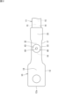
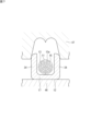
- FIG. 1 is a plan view showing a first embodiment of an electric wire with a terminal.
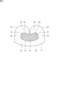
- FIG. 2 is a bottom view of the electric wire with terminal shown in FIG.
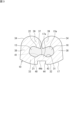
- FIG. 3 is a cross-sectional view taken along the line III-III in FIG.
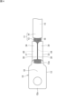
- FIG. 4 is a plan view showing a second embodiment of an electric wire with a terminal.
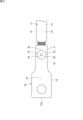
- FIG. 5 is a bottom view of the electric wire with terminal shown in FIG.
- FIG. 6 is an explanatory diagram of friction stir spot welding and its tool.
- FIG. 7 is an explanatory diagram of the method for manufacturing an electric wire with a terminal (preparation step and crimping step).
- FIG. 8 is a cross-sectional view of the electric wire with terminal after the crimping process is completed.
- FIG. 9 is an explanatory diagram of a manufacturing method (joining step) of an electric wire with a terminal.
- ⁇ Problem to be solved by the invention> For example, when electric vehicles and other vehicles use large currents, the diameter of the electric wire with terminal used increases accordingly. In general, when the diameter of the electric wire increases, the force that peels the end of the electric wire from the terminal increases when the electric wire is bent. For this reason, it is necessary to increase the connection strength between the terminal and the electric wire. Furthermore, it is necessary to reduce the electrical resistance of the electric wire with terminal. Although ultrasonic welding is used to connect the terminal and the electric wire, the peel strength may be weak if the welding is used alone.
- the terminal has a bottom wall portion on which the conductor (end of the electric wire) is placed, and a crimping portion for plastically deforming the conductor to crimp it to the terminal. Both the bottom wall portion and the crimping portion are caused to plastically flow together with the conductor, connecting the conductor and the terminal.
- the conductor is plastically flowed by friction stir welding. This can cause the conductor to become distorted, reducing the product value. In particular, if the conductor is a twisted wire, the distorts significantly.
- the present disclosure therefore aims to provide an electric wire with a terminal that can improve the connection strength between the terminal and the electric wire and reduce electrical resistance while keeping the conductor of the electric wire in a neat state, and a method for manufacturing the same.
- the electric wire with terminal of this embodiment comprises an electric wire having a conductor and an insulating coating covering the conductor, and a terminal connected to an end of the electric wire, wherein the conductor has a conductor end exposed from the insulating coating, and the terminal has a terminal base in contact with the conductor end and a crimping portion for crimping the conductor end to the terminal base, the terminal base has a first terminal surface in contact with the conductor end and a second terminal surface opposite the first terminal surface, the second terminal surface has an indentation, and the first terminal surface has a raised surface that protrudes toward the conductor end at a position opposite the indentation in the plate thickness direction.
- the conductor end and the terminal base are mechanically connected by the crimping portion, improving the connection strength. Furthermore, by generating an indentation on the second terminal surface of the terminal base, for example, by friction stir spot welding, a metal-to-metal bond is obtained at least in part between the terminal base and the conductor end. This makes it possible to reduce the electrical resistance between the terminal base and the conductor end.
- the first terminal surface has a raised surface due to friction stir spot welding, and the plastic flow caused by the friction stir spot welding does not extend beyond the first terminal surface to the conductor end, so that the conductor is in a neat state.
- the indentation has a recess that is recessed toward the conductor end portion, and the bottom of the recess is located within the plate thickness range of the terminal base. According to the above-mentioned configuration, the recess does not penetrate the terminal base, i.e., the plastic flow caused by the friction stir spot welding does not extend beyond the first terminal surface to the conductor end.
- the indentation and the crimped portion are at the same position in the longitudinal direction of the electric wire.
- At least a part of the joint between the terminal base and the conductor end portion has a solid-state joint.
- a metallurgical bond is achieved at least in part between the terminal base and the conductor end, and over time, electrical resistance between the terminal base and the conductor end is reduced.
- the electric wire is an aluminum electric wire, and the terminal is a copper terminal.
- the conductor is made of an aluminum alloy, and the terminal is made of a copper alloy. Even with such a combination of dissimilar materials, it is expected that at least a part of the conductor end portion will be joined by destroying the oxide film.
- the conductor is preferably a stranded wire in which a plurality of core wires are twisted together. The core wires do not come apart and remain bundled.
- the conductor may be a single-core wire.
- the manufacturing method of an electric wire with terminal of this embodiment is a manufacturing method of an electric wire with terminal having an electric wire having a conductor and an insulating coating covering the conductor, and a terminal to be connected to the end of the electric wire, and includes a preparation step of overlapping the end of the conductor on the terminal with the end of the conductor exposed from the insulating coating, a crimping step of crimping the end of the conductor to the terminal by a crimping portion of the terminal, and a joining step of friction stir spot joining the end of the conductor and the terminal by contacting a tool with the surface of the terminal opposite the crimping portion, and the plastic flow caused by the friction stir spot joining is performed within the range of the terminal without reaching the end of the conductor.
- the end of the conductor and the terminal are mechanically connected by the crimped portion, improving the connection strength.
- Friction stir spot welding provides a metal-to-metal bond at least partially between the terminal and the end of the conductor. This makes it possible to reduce the electrical resistance between the terminal and the conductor. The plastic flow caused by friction stir spot welding does not extend beyond the terminal to the end of the conductor. This results in a neat conductor.
- FIG. 1 is a plan view showing a first embodiment of an electric wire with terminal.
- Fig. 2 is a bottom view of the electric wire with terminal shown in Fig. 1.
- Fig. 3 is a cross-sectional view taken along the line III-III in Fig. 1.
- the electric wire with terminal 10 is used as an electric wire for supplying power in various devices such as automobiles, and in this embodiment, is used in an electric vehicle.
- the electric wire with terminal 10 is used, for example, in a path for supplying power from a battery to an in-vehicle device.
- the electric wire with terminal 10 has an electric wire 11 and a terminal 12 that is connected to an end of the electric wire 11.
- the terminal 12 is mechanically and electrically connected to a mating terminal (not shown).
- the electric wire 11 has a conductor 13 and an insulating coating 14 that covers the conductor 13.
- the conductor 13 is exposed at an end of the electric wire 11. That is, the conductor 13 has a conductor main body 15 surrounded by the insulating coating 14 and a conductor end 16 exposed from the insulating coating 14.
- the conductor 13 shown in Fig. 1 is a twisted wire in which a plurality of core wires 13a are twisted.
- the conductor 13 is connected to the terminal 12 at the conductor end 16.
- the conductor 13 may be a single-core wire composed of a single wire.
- the terminal 12 and the conductor 13 are made of a material with excellent conductivity.
- the terminal 12 is made of a copper alloy
- the conductor 13 is made of an aluminum alloy. That is, the terminal 12 is a copper terminal, and the electric wire 11 is an aluminum electric wire.
- the insulating coating 14 is made of an insulating material with excellent flame retardancy, for example, cross-linked polyethylene (PE) or polyvinyl chloride (PVC).
- PE cross-linked polyethylene
- PVC polyvinyl chloride
- the terminal 12, the conductor 13, and the insulating coating 14 may be made of other materials.
- the terminal 12 and the conductor 13 may be made of the same material, or may be made of different materials.
- the longitudinal direction of the electric wire with terminal 10 coincides with the longitudinal direction of the electric wire 11.
- the longitudinal direction of the electric wire 11 is defined as the "front-rear direction”
- the side of the tip 12a of the terminal 12 is defined as the "front.”
- the terminal 12 has a pair of first crimping portions 34.
- the direction in which the pair of first crimping portions 34 are arranged is perpendicular to the front-rear direction, and this direction is defined as the "width direction.”
- the direction perpendicular to both the front-rear direction and the width direction is defined as the "up-down direction.”
- this up-down direction is the direction when the terminal-attached electric wire 10 is arranged in a straight line along an imaginary horizontal plane in order to explain the configuration of the terminal-attached electric wire 10 of the present disclosure. Needless to say, when the terminal-attached electric wire 10 is actually used, the up-down direction may not coincide with the vertical direction.
- the terminal 12 has a terminal tip portion 18, a terminal base portion 17, and a first crimping portion 34.
- the terminal 12 has a second crimping portion 36.
- the terminal 12 is formed by processing a plate-shaped metal member (a plate material made of a copper alloy).
- the terminal tip 18 is a portion that can be electrically connected to a mating terminal (not shown) and is plate-like and has a flat shape.
- the terminal base 17 is a portion that is continuous with the terminal tip 18 in the front-to-rear direction.
- the terminal base 17 contacts the conductor end 16.
- the first crimping portion 34 and the second crimping portion 36 are portions for mechanically connecting the electric wire 11 to the terminal 12.
- the terminal base 17 (see FIG. 2) has a first bottom wall portion 33 that is continuous with the terminal tip portion 18 in the front-to-rear direction, and a second bottom wall portion 35 that is continuous with the first bottom wall portion 33 in the front-to-rear direction.
- the terminal base 17 has a first terminal surface 31 in contact with the conductor end portion 16 at the first bottom wall portion 33 (see FIG. 3), and a second terminal surface 32 on the opposite side of the first terminal surface 31 in the up-down direction.
- the second terminal surface 32 has an indentation 40.
- the second terminal surface 32 is recessed at the center in the front-rear direction and the center in the width direction within the range of the indentation 40. More specifically, the indentation 40 has a recess 44 recessed toward the conductor end 16. In other words, the second terminal surface 32 has, at its center, the indentation 40 including the recess 44 recessed toward the conductor end 16.
- the first terminal surface 31 is raised at the center in the front-rear direction and the center in the width direction. That is, the first terminal surface 31 has a raised surface 37 at its center.
- the raised surface 37 is raised toward the conductor end portion 16 at a position opposite the indentation 40.
- the "opposite position” refers to the opposite position in the plate thickness direction (i.e., the up-down direction) of the terminal base 17.
- the first crimping portion 34 extends from a part of the terminal base 17 (the first bottom wall portion 33) and is a portion that is plastically deformed to connect the electric wire 11 and the terminal 12.
- the first crimping portion 34 is crimped to the conductor end 16, thereby crimping the conductor end 16 to the terminal base 17.
- the first crimping portion 34 has side wall portions 38 that rise from both sides of the first bottom wall portion 33 in the width direction, and a tip portion 39 that extends from the side wall portions 38 toward the center in the width direction.
- the first crimping portion 34 is configured by plastic deformation, and the tip portion 39 is in a state in which the conductor end portion 16 is sandwiched between the first bottom wall portion 33.
- the first bottom wall portion 33, the left and right side wall portions 38, and the left and right tip portions 39 are each in close contact with the conductor end portion 16.
- the second bottom wall portion 35 (see FIGS. 1 and 2 ) is a portion that extends rearward from the first bottom wall portion 33 and is in contact with the insulating coating 14 .
- the second crimping portion 36 extends from the second bottom wall portion 35 and is a portion that is plastically deformed to connect the electric wire 11 and the terminal 12.
- the second crimping portion 36 extends upward from both sides of the second bottom wall portion 35 in the width direction and is crimped against the insulating coating 14 to fix the electric wire 11 to the terminal 12.
- the second crimping portion 36 is also called an insulation barrel.
- the second crimping portion 36 fixes the terminal 12 to the electric wire 11 by sandwiching a portion of the electric wire 11 having the insulating coating 14 between the second crimping portion 36 and the second bottom wall portion 35.
- the terminal tip 18 may be tin-plated.
- the tin plating may be applied to the entire terminal 12, including the terminal base 17. In this case, masking is not required when tin-plating the terminal 12, and production efficiency is high. Only the terminal tip 18 may be tin-plated.
- the conductor end 16 of the electric wire 11 will be further described.
- the conductor end 16 has a shape that conforms to the shapes of the first bottom wall portion 33 and the first crimping portion 34 (left and right side wall portions 38 and left and right tip portions 39).
- the conductor end 16 has a first conductor surface 21 that contacts the first bottom wall portion 33 of the terminal base 17, and a second conductor surface 22 that is opposite the first conductor surface 21 in the up-down direction.
- the first conductor surface 21 is recessed along a raised surface 37 at its center.
- the tip portion 39 of the first crimping portion 34 is in a state of being bitten into the second conductor surface 22.
- the first terminal surface 31 and the first conductor surface 21 are joined. At least a part of the joint between the first terminal surface 31 and the first conductor surface 21 includes a solid-state welded portion 41. That is, the conductor end portion 16 and the first bottom wall portion 33 are partially solid-state welded. In the solid-state welded range, the conductor end portion 16 and the terminal base portion 17 are metallically joined, and there is no joint interface between the conductor end portion 16 and the terminal base portion 17.
- the solid-state welding is preferably performed on the entire first bottom wall portion 33 (first terminal surface 31) and the conductor end portion 16 (first conductor surface 21), but may be performed only partially. In other words, it is sufficient that the terminal base portion 17 has the solid-state welding portion 41 on at least a part of the first terminal surface 31 side.
- the conductor end 16 and the side wall portion 38 of the first crimping portion 34 are not solid-state welded to each other.
- the conductor end 16 and the tip portion 39 of the first crimping portion 34 are not solid-state welded to each other.
- the conductor end 16 and the terminal base 17 are partially solid-state welded.
- the terminal base 17 and the conductor end 16 are integrated by the first crimping portion 34, and friction stir spot welding is performed on the terminal base 17 (see FIG. 6).
- friction stir spot welding a rotating tool 50 is brought into contact with and pressed against the second terminal surface 32. This forms an indentation 40 on the second terminal surface 32 (see FIGS. 2 and 3), and at least a portion of the area directly above the indentation 40 is solid-state welded.
- the tool 50 has a cylindrical shoulder 51 and a cylindrical pin 52 protruding from the shoulder 51.
- the pin 52 has an outer diameter smaller than that of the shoulder 51.
- the rotating tool 50 is pressed against the terminal base 17, and the pin 52 is pressed into the terminal base 17.
- the conductor end 16 and the terminal base 17 are heated by frictional heat generated between the rotating tool 50 and the terminal base 17, a portion of the space between the first conductor surface 21 and the first terminal surface 31 is metallically bonded, and a portion of the conductor end 16 and the terminal base 17 are solid-state welded.
- the jig 53 supports the pressing force applied by the tool 50 to the terminal base 17.
- the conductor end 16 and the tip 39 of the first crimping portion 34 are sandwiched between the terminal base 17 and the jig 53.
- the conductor end portion 16 is made of a twisted wire.
- the adjacent core wires 13a included in the twisted wire are also in close contact with each other (see FIG. 3). It is preferable that adjacent core wires 13a included in the twisted wire are also partially solid-state joined together by the heat and pressure applied by friction stir spot joining, but the core wires 13a do not have to be solid-state joined together.
- the indentation 40 has a recess 44 recessed toward the conductor end 16 side by the pin 52.
- the protruding length L of the pin 52 is smaller than the thickness t of the first bottom wall portion 33 of the terminal base 17. Therefore, as shown in FIG. 3, the bottom 44b of the recess 44 is formed by the first bottom wall portion 33 crushed by the pin 52. More specifically, the bottom 44b is located within the plate thickness range of the terminal base 17 (first bottom wall portion 33). In other words, the bottom 44b is formed by the terminal layer 17a, which is a part of the deformed first bottom wall portion 33.
- the first terminal surface 31 is partially raised toward the conductor end 16.
- the raised surface 37 is formed in an area that includes the position directly above the indentation 40.
- the conductor end 16 is recessed according to the raised shape of the raised surface 37.
- the indentation 40 has a deep recess 44 in its center and a pressing portion 43 around the recess 44.
- the recess 44 is formed by contact with the pin 52 of the tool 50, and is circular as shown in Fig. 2.
- the pressing portion 43 is formed by contact with the shoulder 51 of the tool 50, and is annular.
- the tool 50 does not come into contact with the entire second terminal surface 32 but only partially comes into contact with the second terminal surface 32.
- the tool 50 comes into contact with an area including the center of the second terminal surface 32 in the front-rear direction and the center of the second terminal surface 32 in the width direction.
- the indentation 40 and the first crimping portion 34 are at the same position in the longitudinal direction (front-to-back direction) of the electric wire 11 (see FIG. 1).
- the indentation 40 is located on the lower side of the terminal 12, the tip 39 of the first crimping portion 34 is located on the upper side of the terminal 12, and the indentation 40 is located on the opposite side in the up-down direction to the tip 39 of the first crimping portion 34.
- Second Embodiment Fig. 4 is a plan view showing a second embodiment of the electric wire with terminal 10.
- Fig. 5 is a bottom view of the electric wire with terminal 10 shown in Fig. 4.
- the electric wire with terminal 10 shown in Figs. 4 and 5 is different from the first embodiment shown in Figs. 1 and 2 in that it does not have the second bottom wall portion 35 and the second crimping portion 36, but is otherwise the same.
- the same components are denoted by the same reference numerals, and the description thereof will be omitted here.
- the terminal base 17 is located away from the insulating coating 14 of the electric wire 11.
- the cross-sectional shape of the terminal base 17 and the first crimped portion 34 where the indentation 40 is formed is the same as in the first embodiment (Fig. 3). That is, the second terminal surface 32 of the terminal base 17 has the indentation 40.
- the first terminal surface 31 of the terminal base 17 has a raised surface 37 that is raised toward the conductor end 16 at a position opposite the indentation 40.
- the manufacturing method includes a preparation step, a crimping step, and a joining step.
- a crimping step for example, a crimping device having a base 46 and a die 47 (see FIG. 7) is used.
- the conductor end 16 of the electric wire 11 is overlapped on the terminal base 17 of the terminal 12 in a state in which the conductor end 16 is exposed from the insulating coating 14.
- the terminal base 17 of the terminal 12 and the conductor end 16 of the electric wire 11 are overlapped on a base 46.
- a pressurizing device presses a die 47 against the terminal 12 and the electric wire 11 on the base 46.
- the die 47 plastically deforms the pair of first crimping portions 34.
- the conductor end 16 is crimped to the terminal base 17 by the first crimping portions 34 of the terminal 12 (see FIG. 8 ).
- the second crimped portion 36 is plastically deformed by the same operation as the crimping device, either simultaneously with the first crimped portion 34 or at a different timing from the first crimped portion 34.
- the tip 39 of the first crimped portion 34 is received by a jig 53.
- a tool 50 is brought into contact with the second terminal surface 32, which is the surface of the terminal 12 opposite the tip 39 of the first crimped portion 34, to friction stir spot join the conductor end 16 and the terminal base 17.
- the plastic flow caused by friction stir spot welding occurs within the range of the plate thickness of the terminal 12 (terminal base 17) without reaching the conductor end 16.
- the plastic flow caused by friction stir spot welding does not extend beyond the terminal base 17 to the conductor end 16. Therefore, the conductor 13 is in a neat state.
- the conductor 13 is a stranded wire in which a plurality of core wires (strands) 13a are stranded. Even in this case, the core wires 13a do not come apart and are maintained in a bundled state by friction stir spot joining. The conductor 13 is in a neat state.
- a gap is likely to occur between the core wires 13a of the twisted wire and the terminal base 17.
- the connection between the terminal base 17 and the conductor end 16 is based on a force accompanied by an indentation 40, the gap disappears and the two are in close contact with each other. Furthermore, the gaps between adjacent core wires 13a also disappear, and the two are in close contact with each other.
- the tip 39 of the first crimping portion 34 plastically deformed in the crimping process has an arc shape that is convex toward the side away from the conductor end 16. Therefore, as shown in Fig. 9, the jig 53 may have a concave arc shape corresponding to the shape of the tip 39 of the first crimping portion 34.
- the conductor end 16 sandwiched between the terminal base 17 and the tip 39 of the first crimping portion 34 tends to expand in the width direction.
- the side wall portions 38 on both sides in the width direction of the first crimping portion 34 can regulate the expansion of the conductor end 16 in the width direction.
- the jig 53 makes it possible to perform friction stir spot welding while maintaining the shape of the first crimped portion 34.
- the electric wire with terminal 10 of each of the above-mentioned embodiments includes the electric wire 11 and the terminal 12 connected to the end of the electric wire 11.
- the conductor 13 of the electric wire 11 has the conductor end 16 exposed from the insulating coating 14.
- the terminal 12 has a terminal base 17 in contact with the conductor end 16, and a first crimping portion 34 for crimping the conductor end 16 to the terminal base 17.
- the terminal base 17 has a first terminal surface 31 in contact with the conductor end 16, and a second terminal surface 32 opposite the first terminal surface 31.
- the second terminal surface 32 has an indentation 40.
- the first terminal surface 31 has a raised surface 37 that is raised toward the conductor end 16 at a position opposite the indentation 40 in the plate thickness direction.
- the conductor end portion 16 and the terminal base portion 17 are mechanically connected to each other by the first crimping portion 34, thereby improving the connection strength.
- the friction stir spot welding creates an indentation 40 on the second terminal surface 32 of the terminal base 17. This provides a metal-to-metal bond at least partially between the terminal base 17 and the conductor end 16. As a result, it is possible to reduce the electrical resistance between the terminal base 17 and the conductor end 16. Even without ultrasonic welding, the connection strength between the conductor end 16 and the terminal base 17 is improved, and it is possible to reduce the electrical resistance between the conductor end 16 and the terminal base 17. Due to the friction stir spot welding, the first terminal surface 31 has a raised surface 37, and the plastic flow caused by the friction stir spot welding does not extend beyond the first terminal surface 31 to the conductor end 16. Therefore, the conductor 13 is in a neat state.
- the plastic flow caused by friction stir spot welding does not extend beyond the first terminal surface 31 to the conductor end. For this reason, as shown in FIG. 3, the recess 44 does not penetrate the terminal base 17.
- the impression 40 has a recess 44 that is recessed toward the conductor end 16, and the bottom 44b of the recess 44 is located within the plate thickness range of the terminal base 17.
- At least a portion of the joint between the terminal base 17 and the conductor end 16 has a solid-state weld 41.
- a durability test performed by applying a thermal shock showed that without the solid-state weld 41, a poor connection would eventually occur and electrical resistance would increase.
- a metal-to-metal bond is obtained at least partially between the terminal base 17 and the conductor end 16, which reduces the electrical resistance between the terminal base 17 and the conductor end 16 over the long term.
- the electric wire 11 is an aluminum electric wire
- the terminal 12 is a copper terminal.
- the strength of the mechanical connection between the electric wire 11 and the terminal 12 is ensured by the crimping by the first crimping portion 34.
- the oxide film of the electric wire 11 at the conductor end 16 is not removed by this crimping alone. Therefore, in the case of each of the above-mentioned embodiments, friction stir spot welding is performed from the second terminal surface 32 side of the terminal base 17, so that the second terminal surface 32 has an indentation 40. This destroys the oxide film on a part of the first conductor surface 21 of the conductor end 16. As a result, the contact resistance between the conductor end 16 and the terminal base 17 is reduced, and the contact resistance can be stabilized for a long period of time.
- the friction stir spot welding may be of the double action type.
- the impression 40 may not have the recess 44 as shown in FIG. 3, or may be a recess smaller than the recess 44 as shown in FIG. 3.
- the terminal 12 has a second crimped portion 36 that is crimped to the insulating coating 14.
- the force that tends to peel the conductor end 16 from the terminal base 17, which occurs when the electric wire 11 is bent in a portion close to the terminal 12 is reduced.
- the connection strength between the terminal 12 and the electric wire 11 is further increased.
- the terminal-attached electric wire 10 of each of the above-mentioned configurations provides high mechanical and electrical reliability for the connection between the electric wire 11 and the terminal 12.
- the electric wire 11 is an aluminum electric wire
- the terminal 12 is a copper terminal.
- the electric wire 11 may be a copper electric wire.
- a tin-plated wire can be used to stabilize the contact resistance.
- the terminal-attached electric wire 10 is formed by crimping with the first crimping portion 34 and friction stir spot joining, which may make it possible to eliminate the need for tin plating of the wire. In particular, it is possible to stabilize the contact resistance even in the case of a thick copper electric wire having a large diameter.
- only one indentation 40 is formed on the second terminal surface 32.
- a plurality of indentations 40 may be provided.
- the plurality of indentations 40 are provided side by side in the front-rear direction.
- the recess 44 of the indentation 40 is a circular hole in a plan view. This "circle" may be a perfect circle or an ellipse.
- the rotating tool 50 may be moved in the front-rear direction, and in this case, the shape of the recess 44 formed is an ellipse.
Landscapes
- Engineering & Computer Science (AREA)
- Manufacturing & Machinery (AREA)
- Connections Effected By Soldering, Adhesion, Or Permanent Deformation (AREA)
- Manufacturing Of Electrical Connectors (AREA)
Abstract
端子付き電線は、導体及び前記導体を覆う絶縁被膜を有する電線と、前記電線の端部と接続する端子と、を有する。前記導体は、前記絶縁被膜から露出する導体端部を有する。前記端子は、前記導体端部と接する端子基部と、前記端子基部に前記導体端部を圧着するためのカシメ部と、を有する。前記端子基部は、前記導体端部と接する第一端子面と、前記第一端子面と反対側の第二端子面と、を有する。前記第二端子面は、圧痕を有する。前記第一端子面は、前記圧痕の板厚方向反対側の位置に前記導体端部側に隆起している隆起面を有する。
Description
本開示は、端子付き電線、及び、その製造方法に関する。本出願は、2023年1月20日出願の日本出願第2023-7052号に基づく優先権を主張し、前記日本出願に記載された全ての記載内容を援用するものである。
特許文献1に、電線と、その電線の端部に接続される端子とを有する端子付き電線が開示されている。端子が相手端子に固定されている状態で、電線を湾曲させると、端子から電線の端部を引き剥がす力が作用する。端子付き電線において、端子と電線との接続力が前記のような引き剥がす力に抗することが必要とされる。
本開示の実施形態に係る端子付き電線は、導体及び前記導体を覆う絶縁被膜を有する電線と、前記電線の端部と接続する端子と、を有し、前記導体は、前記絶縁被膜から露出する導体端部を有し、前記端子は、前記導体端部と接する端子基部と、前記端子基部に前記導体端部を圧着するためのカシメ部と、を有し、前記端子基部は、前記導体端部と接する第一端子面と、前記第一端子面と反対側の第二端子面と、を有し、前記第二端子面は、圧痕を有し、前記第一端子面は、前記圧痕の板厚方向反対側の位置に前記導体端部側に隆起している隆起面を有する。
本開示の実施形態に係る端子付き電線の製造方法は、導体及び前記導体を覆う絶縁被膜を有する電線と、前記電線の端部と接続する端子と、を有する端子付き電線の製造方法であって、前記絶縁被膜から前記導体の端部を露出させた状態で前記導体の端部を前記端子に重ねる準備工程と、前記端子が有するカシメ部により、前記導体の端部を前記端子に圧着する圧着工程と、前記端子のうち、前記カシメ部と反対側の面に対してツールを接触させて前記導体の端部と前記端子とを摩擦攪拌スポット接合する接合工程と、を含み、前記摩擦撹拌スポット接合による塑性流動は、前記導体の端部に及ばないで前記端子の範囲で行われる。
<発明が解決しようとする課題>
例えば電気自動車などの車両において大電流化が進むと、これに対応すべく、用いられる端子付き電線は大径化する。一般的に、電線が大径化すると、例えばその電線を湾曲させた際に、端子から電線の端部を引き剥がす力が大きくなる。このため、端子と電線との接続強度を高めることが必要とされる。さらに、端子付き電線における電気抵抗を低減することが必要とされる。なお、端子と電線との接続のために超音波溶接が用いられるが、その溶接のみであると、引き剥がし強度が弱い場合がある。
例えば電気自動車などの車両において大電流化が進むと、これに対応すべく、用いられる端子付き電線は大径化する。一般的に、電線が大径化すると、例えばその電線を湾曲させた際に、端子から電線の端部を引き剥がす力が大きくなる。このため、端子と電線との接続強度を高めることが必要とされる。さらに、端子付き電線における電気抵抗を低減することが必要とされる。なお、端子と電線との接続のために超音波溶接が用いられるが、その溶接のみであると、引き剥がし強度が弱い場合がある。
前記特許文献1の場合、端子は、導体(電線の端部)が配置される底壁部と、塑性変形させて導体を端子に圧着するためのカシメ部とを有する。底壁部及びカシメ部の双方を、導体と共に塑性流動させ、導体と端子とを接続する。前記特許文献1の場合、摩擦撹拌接合により、導体が塑性流動する。このため、導体は乱れ、製品価値が低下する可能性がある。特に、導体が撚り線である場合、大きく乱れる。
そこで、本開示は、端子と電線との接続強度の向上及び電気抵抗の低減が可能であると共に、電線の導体を整った状態とする端子付き電線、及び、その製造方法を提供することを目的とする。
<発明の効果>
本開示によれば、端子と電線との接続強度の向上及び電気抵抗の低減が可能であると共に、電線の導体が整った状態となる。
本開示によれば、端子と電線との接続強度の向上及び電気抵抗の低減が可能であると共に、電線の導体が整った状態となる。
<本開示の実施形態の概要>
以下、本開示の実施形態の概要を列記して説明する。
(1)本実施形態の端子付き電線は、導体及び前記導体を覆う絶縁被膜を有する電線と、前記電線の端部と接続する端子と、を有し、前記導体は、前記絶縁被膜から露出する導体端部を有し、前記端子は、前記導体端部と接する端子基部と、前記端子基部に前記導体端部を圧着するためのカシメ部と、を有し、前記端子基部は、前記導体端部と接する第一端子面と、前記第一端子面と反対側の第二端子面と、を有し、前記第二端子面は、圧痕を有し、前記第一端子面は、前記圧痕の板厚方向反対側の位置に前記導体端部側に隆起している隆起面を有する。
以下、本開示の実施形態の概要を列記して説明する。
(1)本実施形態の端子付き電線は、導体及び前記導体を覆う絶縁被膜を有する電線と、前記電線の端部と接続する端子と、を有し、前記導体は、前記絶縁被膜から露出する導体端部を有し、前記端子は、前記導体端部と接する端子基部と、前記端子基部に前記導体端部を圧着するためのカシメ部と、を有し、前記端子基部は、前記導体端部と接する第一端子面と、前記第一端子面と反対側の第二端子面と、を有し、前記第二端子面は、圧痕を有し、前記第一端子面は、前記圧痕の板厚方向反対側の位置に前記導体端部側に隆起している隆起面を有する。
前記端子付き電線によれば、導体端部と端子基部とはカシメ部により機械的に接続され、接続強度が向上する。更に、例えば摩擦撹拌スポット接合により、端子基部の第二端子面に圧痕を生じさせることで、端子基部と導体端部との間の少なくとも一部で金属間接合が得られる。このため、端子基部と導体端部との間の電気抵抗を低減することが可能となる。
例えば摩擦撹拌スポット接合により、第一端子面は隆起面を有しており、その摩擦撹拌スポット接合による塑性流動は、第一端子面を越えて導体端部に及ばない。このため、導体は整った状態となる。
例えば摩擦撹拌スポット接合により、第一端子面は隆起面を有しており、その摩擦撹拌スポット接合による塑性流動は、第一端子面を越えて導体端部に及ばない。このため、導体は整った状態となる。
(2)好ましくは、前記圧痕は、前記導体端部側に凹む凹部を有し、前記凹部の底は、前記端子基部の板厚範囲内に位置している。
前記構成によれば、凹部は端子基部を貫通しない。つまり、摩擦撹拌スポット接合による塑性流動は、第一端子面を越えて導体端部に及ばない。
前記構成によれば、凹部は端子基部を貫通しない。つまり、摩擦撹拌スポット接合による塑性流動は、第一端子面を越えて導体端部に及ばない。
(3)前記(1)又は(2)の端子付き電線において、端子と電線との接続強度を高めるために、好ましくは、前記圧痕と前記カシメ部とは、前記電線の長手方向について同じ位置にある。
(4)前記(1)から(3)のいずれか一つの端子付き電線において、好ましくは、前記端子基部と前記導体端部との間の接合部の少なくとも一部は、固相接合部を有する。
端子基部と導体端部との間の少なくとも一部で金属間接合が得られる。長期にわたって、端子基部と導体端部との間の電気抵抗が低減する。
端子基部と導体端部との間の少なくとも一部で金属間接合が得られる。長期にわたって、端子基部と導体端部との間の電気抵抗が低減する。
(5)前記(1)から(4)のいずれか一つの端子付き電線において、好ましくは、前記電線は、アルミ電線であり、前記端子は、銅端子である。
前記導体は、アルミニウム合金からなり、前記端子は、銅合金からなる。このような異種材料の組み合わせであっても、導体端部の少なくとも一部は、酸化皮膜が破壊されて接合されることが期待される。
前記導体は、アルミニウム合金からなり、前記端子は、銅合金からなる。このような異種材料の組み合わせであっても、導体端部の少なくとも一部は、酸化皮膜が破壊されて接合されることが期待される。
(6)前記(1)から(5)のいずれか一つの端子付き電線において、好ましくは、前記導体は、複数の芯線が撚られた撚り線である。
芯線はばらつかず、纏まった状態に維持される。
(7)前記(1)から(5)のいずれか一つの端子付き電線において、前記導体は、単芯線であってもよい。
芯線はばらつかず、纏まった状態に維持される。
(7)前記(1)から(5)のいずれか一つの端子付き電線において、前記導体は、単芯線であってもよい。
(8)本実施形態の端子付き電線の製造方法は、導体及び前記導体を覆う絶縁被膜を有する電線と、前記電線の端部と接続する端子と、を有する端子付き電線の製造方法であって、前記絶縁被膜から前記導体の端部を露出させた状態で前記導体の端部を前記端子に重ねる準備工程と、前記端子が有するカシメ部により、前記導体の端部を前記端子に圧着する圧着工程と、前記端子のうち、前記カシメ部と反対側の面に対してツールを接触させて前記導体の端部と前記端子とを摩擦攪拌スポット接合する接合工程と、を含み、前記摩擦撹拌スポット接合による塑性流動は、前記導体の端部に及ばないで前記端子の範囲で行われる。
前記製造方法によれば、導体の端部と端子とはカシメ部により機械的に接続され、接続強度が向上する。摩擦撹拌スポット接合により、端子と導体の端部との間の少なくとも一部で金属間接合が得られる。このため、端子と導体との間の電気抵抗を低減することが可能となる。摩擦撹拌スポット接合による塑性流動は、端子を越えて導体の端部に及ばない。このため、導体は整った状態となる。
<本開示の実施形態の詳細>
以下、図面を参照して、本開示の実施形態の詳細を説明する。なお、以下に記載する実施形態の少なくとも一部を任意に組み合わせてもよい。
以下、図面を参照して、本開示の実施形態の詳細を説明する。なお、以下に記載する実施形態の少なくとも一部を任意に組み合わせてもよい。
〔端子付き電線の全体構成について〕
図1は、端子付き電線の第一実施形態を示す平面図である。図2は、図1に示す端子付き電線の底面図である。図3は、図1のIII-III矢視の断面図である。端子付き電線10は、電力供給用の電線として自動車等の様々な装置に用いられ、本実施形態では電気自動車に用いられる。端子付き電線10は、例えばバッテリから車載機器に電力を供給する経路に用いられる。
図1は、端子付き電線の第一実施形態を示す平面図である。図2は、図1に示す端子付き電線の底面図である。図3は、図1のIII-III矢視の断面図である。端子付き電線10は、電力供給用の電線として自動車等の様々な装置に用いられ、本実施形態では電気自動車に用いられる。端子付き電線10は、例えばバッテリから車載機器に電力を供給する経路に用いられる。
端子付き電線10は、電線11と、電線11の端部と接続する端子12とを有する。端子12は、相手端子(図示せず)と機械的及び電気的に接続される。
電線11は、導体13と、導体13を覆う絶縁被膜14とを有する。導体13は、電線11の端部で露出している。つまり、導体13は、絶縁被膜14に囲われている導体本体部15と、絶縁被膜14から露出する導体端部16とを有する。図1に示す導体13は、複数の芯線13aが撚られた撚り線である。導体13は、導体端部16において端子12と接続されている。なお、導体13は、1本の線で構成される単芯線であってもよい。
電線11は、導体13と、導体13を覆う絶縁被膜14とを有する。導体13は、電線11の端部で露出している。つまり、導体13は、絶縁被膜14に囲われている導体本体部15と、絶縁被膜14から露出する導体端部16とを有する。図1に示す導体13は、複数の芯線13aが撚られた撚り線である。導体13は、導体端部16において端子12と接続されている。なお、導体13は、1本の線で構成される単芯線であってもよい。
端子12及び導体13は、導電性の優れる材料により構成されている。本実施形態の場合、端子12は銅合金からなり、導体13はアルミニウム合金からなる。つまり、端子12は銅端子であり、電線11はアルミ電線である。絶縁被膜14は、難燃性に優れる絶縁性材料により構成されていて、例えば、架橋ポリエチレン(PE)又はポリ塩化ビニル(PVC)が用いられる。なお、端子12、導体13、及び絶縁被膜14の材質は他であってもよい。端子12及び導体13は、異種材料である他に、同じ材料であってもよい。
本開示の端子付き電線10の各方向について定義する。端子付き電線10の長手方向は、電線11の長手方向と一致する。電線11を直線状として配置した場合に、その電線11の長手方向を「前後方向」と定義し、端子12の先端12a側を「前」と定義する。
端子12は、後に説明するが、一対の第一カシメ部34を有する。一対の第一カシメ部34が並ぶ方向は、前後方向に直交する方向であり、この方向を「幅方向」と定義する。
端子12は、後に説明するが、一対の第一カシメ部34を有する。一対の第一カシメ部34が並ぶ方向は、前後方向に直交する方向であり、この方向を「幅方向」と定義する。
前後方向及び幅方向の双方に直交する方向を「上下方向」と定義する。なお、この上下方向は、本開示の端子付き電線10の構成を説明するために、仮想の水平面に沿って端子付き電線10を直線状として配置した場合の方向である。言うまでもないが、端子付き電線10が実際に使用される際、前記上下方向は鉛直方向と一致しない場合がある。
〔端子12について〕
端子12は、端子先部18と、端子基部17と、第一カシメ部34とを有する。本実施形態の場合、端子12は、第二カシメ部36を有する。端子12は、板状の金属部材(銅合金による板材)を加工して構成される。
端子12は、端子先部18と、端子基部17と、第一カシメ部34とを有する。本実施形態の場合、端子12は、第二カシメ部36を有する。端子12は、板状の金属部材(銅合金による板材)を加工して構成される。
端子先部18は、相手端子(図示せず)と電気的に接続可能となる部分であり、板状であって、平坦形状を有する。端子基部17は、端子先部18と前後方向に連続する部分である。端子基部17は、導体端部16と接する。第一カシメ部34及び第二カシメ部36は、電線11を端子12に機械的に接続するための部分である。
端子基部17は(図2参照)、端子先部18と前後方向に連続する第一底壁部33と、第一底壁部33と前後方向に連続する第二底壁部35とを有する。端子基部17は、第一底壁部33において(図3参照)、導体端部16と接する第一端子面31と、第一端子面31と上下方向について反対側の第二端子面32とを有する。
第二端子面32は、圧痕40を有する。本実施形態の場合、第二端子面32は、圧痕40の範囲内で、前後方向の中央及び幅方向の中央で凹んでいる。具体的に説明すると、圧痕40は、導体端部16側に凹む凹部44を有する。つまり、第二端子面32は、その中央に、導体端部16側に凹んでいる凹部44を含む圧痕40を有する。
第一端子面31は、その前後方向の中央及び幅方向の中央で隆起している。つまり、第一端子面31は、その中央に、隆起面37を有する。隆起面37は、圧痕40の反対側の位置において、導体端部16側に隆起している。「反対側の位置」とは、端子基部17の板厚方向(つまり、上下方向)について反対側の位置である。
第一端子面31は、その前後方向の中央及び幅方向の中央で隆起している。つまり、第一端子面31は、その中央に、隆起面37を有する。隆起面37は、圧痕40の反対側の位置において、導体端部16側に隆起している。「反対側の位置」とは、端子基部17の板厚方向(つまり、上下方向)について反対側の位置である。
第一カシメ部34は、端子基部17の一部(第一底壁部33)から延びて設けられており、電線11と端子12との接続のために塑性変形させる部分である。第一カシメ部34は、導体端部16に対してカシメられることで、端子基部17に導体端部16を圧着する部分である。
第一カシメ部34は、第一底壁部33の幅方向両側それぞれから立ち上がるようにして設けられている側壁部38と、側壁部38から幅方向の中央に向かって延びる先部39とを有する。導体端部16を端子基部17に圧着させるために、第一カシメ部34は、塑性変形して構成され、先部39は、第一底壁部33との間で導体端部16を挟んだ状態にある。第一底壁部33、左右の側壁部38、及び、左右の先部39それぞれは、導体端部16に密に接触した状態にある。
第二底壁部35は(図1及び図2参照)、第一底壁部33から後方に延びて設けられている部分であり、絶縁被膜14と接する。
第二カシメ部36は、第二底壁部35から延びて設けられており、電線11と端子12との接続のために塑性変形させる部分である。第二カシメ部36は、第二底壁部35の幅方向両側から上に延びて設けられ、絶縁被膜14に対してカシメられることで、端子12に電線11を固定する。第二カシメ部36は、インシュレーションバレルとも呼ばれる。第二カシメ部36は、電線11のうち絶縁被膜14を有する部分を、第二底壁部35との間で挟むことで、端子12を電線11に固定する。
第二カシメ部36は、第二底壁部35から延びて設けられており、電線11と端子12との接続のために塑性変形させる部分である。第二カシメ部36は、第二底壁部35の幅方向両側から上に延びて設けられ、絶縁被膜14に対してカシメられることで、端子12に電線11を固定する。第二カシメ部36は、インシュレーションバレルとも呼ばれる。第二カシメ部36は、電線11のうち絶縁被膜14を有する部分を、第二底壁部35との間で挟むことで、端子12を電線11に固定する。
端子先部18に錫メッキが付されていてもよい。錫メッキは、端子基部17を含む端子12の全体に付されていてもよい。この場合、端子12に錫メッキを付する作業において、マスキングが不要となり生産効率が高い。端子先部18にのみ錫メッキが付されていてもよい。
〔電線11について〕
電線11が有する導体端部16についてさらに説明する。前後方向に直交する横断面において(図3参照)、導体端部16は、第一底壁部33並びに第一カシメ部34(左右の側壁部38及び左右の先部39)の形状に沿った形状を有する。導体端部16は、端子基部17の第一底壁部33と接する第一導体面21と、第一導体面21と上下方向について反対側の第二導体面22とを有する。第一導体面21は、その中央で隆起面37に沿って窪んでいる。第二導体面22に、第一カシメ部34の先部39が食い込んだ状態にある。
電線11が有する導体端部16についてさらに説明する。前後方向に直交する横断面において(図3参照)、導体端部16は、第一底壁部33並びに第一カシメ部34(左右の側壁部38及び左右の先部39)の形状に沿った形状を有する。導体端部16は、端子基部17の第一底壁部33と接する第一導体面21と、第一導体面21と上下方向について反対側の第二導体面22とを有する。第一導体面21は、その中央で隆起面37に沿って窪んでいる。第二導体面22に、第一カシメ部34の先部39が食い込んだ状態にある。
〔電線11と端子12との接続構造について〕
第一端子面31と第一導体面21とは接合されている。第一端子面31と第一導体面21との接合部の少なくとも一部に、固相接合部41が含まれる。つまり、導体端部16と第一底壁部33とは部分的に固相接合されている。固相接合されている範囲では、導体端部16と端子基部17とが金属接合されており、導体端部16と端子基部17との接合界面が無くなっている。
第一端子面31と第一導体面21とは接合されている。第一端子面31と第一導体面21との接合部の少なくとも一部に、固相接合部41が含まれる。つまり、導体端部16と第一底壁部33とは部分的に固相接合されている。固相接合されている範囲では、導体端部16と端子基部17とが金属接合されており、導体端部16と端子基部17との接合界面が無くなっている。
固相接合は、第一底壁部33(第一端子面31)と導体端部16(第一導体面21)との全体で成されているのが好ましいが、部分的に成されていればよい。つまり、端子基部17は、第一端子面31側の少なくとも一部に固相接合部41を有していればよい。
導体端部16と、第一カシメ部34の側壁部38とは固相接合されていない。導体端部16と、第一カシメ部34の先部39とは固相接合されていない。
導体端部16と、第一カシメ部34の側壁部38とは固相接合されていない。導体端部16と、第一カシメ部34の先部39とは固相接合されていない。
前記のとおり、導体端部16と端子基部17とは部分的に固相接合されている。これらの間で固相接合を得るために、本実施形態では、第一カシメ部34によって端子基部17と導体端部16とが一体となる状態で、端子基部17に対して摩擦撹拌スポット接合が行われる(図6参照)。摩擦撹拌スポット接合では、回転するツール50を、第二端子面32に接触させ押し付ける。これにより、第二端子面32に圧痕40が形成され(図2及び図3参照)、その圧痕40の直上位置の少なくとも一部が固相接合される。
ツール50は、円柱状のショルダ51と、ショルダ51から突出する円柱状のピン52とを有する。ピン52はショルダ51よりも外径が小さい。回転するツール50を端子基部17に押し付け、ピン52を端子基部17に圧入する。回転するツール50と端子基部17との間で生じる摩擦熱によって、導体端部16及び端子基部17は加熱され、第一導体面21と第一端子面31との間の一部が金属結合され、導体端部16と端子基部17とは一部において固相接合される。
治具53は、ツール50による端子基部17への押し付け力を支える。導体端部16及び第一カシメ部34の先部39は、端子基部17と治具53とによって挟まれた状態となる。
前記のとおり、導体端部16は撚り線からなる。その撚り線に含まれ隣り合う芯線13a同士においても密着する(図3参照)。
摩擦撹拌スポット接合による加熱と圧力とによって、撚り線に含まれ隣り合う芯線13a同士も部分的に固相接合されるのが好ましいが、芯線13a同士は固相接合されていなくてもよい。
摩擦撹拌スポット接合による加熱と圧力とによって、撚り線に含まれ隣り合う芯線13a同士も部分的に固相接合されるのが好ましいが、芯線13a同士は固相接合されていなくてもよい。
回転するツール50を端子基部17に押し付けることで、ツール50の回転接触面の形状が第二端子面32に転写され、圧痕40が形成される。図3に示すように、ピン52によって、圧痕40は、導体端部16側に凹む凹部44を有する。本実施形態では(図6参照)、ピン52の突出長さLは、端子基部17が有する第一底壁部33の厚さtよりも小さい。このため、図3に示すように、凹部44の底44bは、ピン52により押し潰された第一底壁部33により構成されている。より具体的に説明すると、底44bは、端子基部17(第一底壁部33)の板厚範囲内に位置している。つまり、底44bは、変形した第一底壁部33の一部である端子層17aにより構成されている。
第一端子面31は導体端部16側に部分的に隆起している。隆起面37は、圧痕40の直上位置を含む範囲で形成されている。隆起面37の隆起形状に応じて、導体端部16は窪んでいる。
圧痕40は、その中央に深い凹部44を有し、その凹部44の周囲に押圧部43を有する。凹部44は、ツール50のピン52が接触することで形成され、図2に示すように、円形となる。押圧部43は、ツール50のショルダ51が接触することで形成され、円環状である。
本実施形態の場合、ツール50は、第二端子面32の全体にわたって接触するのではなく、部分的に接触する。ツール50は、第二端子面32の前後方向の中央及び幅方向の中央を含む領域に対して接触する。
本実施形態の場合、ツール50は、第二端子面32の全体にわたって接触するのではなく、部分的に接触する。ツール50は、第二端子面32の前後方向の中央及び幅方向の中央を含む領域に対して接触する。
圧痕40と第一カシメ部34とは、電線11の長手方向(前後方向)について同じ位置にある(図1参照)。圧痕40は、端子12の下側に位置し、第一カシメ部34の先部39は、端子12の上側に位置しており、圧痕40は、第一カシメ部34の先部39の上下方向の反対側に位置する。
〔第二実施形態〕
図4は、端子付き電線10の第二実施形態を示す平面図である。図5は、図4に示す端子付き電線10の底面図である。図4及び図5に示す端子付き電線10は、図1及び図2に示す第一実施形態と比較すると、第二底壁部35及び第二カシメ部36を有していない点で異なるが、その他については同じである。第一実施形態と第二実施形態とで、同じ構成については、同じ符号を付しており、ここでは、その説明を省略する。第二実施形態の場合、端子基部17は、電線11の絶縁被膜14と離れて位置する。
図4は、端子付き電線10の第二実施形態を示す平面図である。図5は、図4に示す端子付き電線10の底面図である。図4及び図5に示す端子付き電線10は、図1及び図2に示す第一実施形態と比較すると、第二底壁部35及び第二カシメ部36を有していない点で異なるが、その他については同じである。第一実施形態と第二実施形態とで、同じ構成については、同じ符号を付しており、ここでは、その説明を省略する。第二実施形態の場合、端子基部17は、電線11の絶縁被膜14と離れて位置する。
第二実施形態の場合においても、圧痕40が形成されている端子基部17及び第一カシメ部34における断面形状は、第一実施形態(図3)と同じである。つまり、端子基部17の第二端子面32は、圧痕40を有する。端子基部17の第一端子面31は、圧痕40の反対側の位置に、導体端部16側に隆起している隆起面37を有する。
〔端子付き電線10の製造方法について〕
端子付き電線10の製造方法について説明する。その製造方法は、準備工程と、圧着工程と、接合工程とを含む。
圧着工程のために、例えば、台座46及び金型47を有する圧着装置(図7参照)が用いられる。
端子付き電線10の製造方法について説明する。その製造方法は、準備工程と、圧着工程と、接合工程とを含む。
圧着工程のために、例えば、台座46及び金型47を有する圧着装置(図7参照)が用いられる。
準備工程では、絶縁被膜14から導体端部16を露出させた状態で、電線11の導体端部16が端子12の端子基部17に重ねられる。図7に示す形態の場合、台座46の上に、端子12の端子基部17と電線11の導体端部16とが重ねられる。
圧着工程では、台座46上の端子12及び電線11に対して、金型47を加圧装置により押圧する。金型47は、一対の第一カシメ部34を塑性変形させる。以上より、圧着工程では、端子12が有する第一カシメ部34により、導体端部16を端子基部17に圧着する(図8参照)。
圧着工程では、台座46上の端子12及び電線11に対して、金型47を加圧装置により押圧する。金型47は、一対の第一カシメ部34を塑性変形させる。以上より、圧着工程では、端子12が有する第一カシメ部34により、導体端部16を端子基部17に圧着する(図8参照)。
端子12が第二カシメ部36を有する場合(図1参照)、前記圧着工程において、第一カシメ部34と同時に、又は、第一カシメ部34とは別のタイミングで、前記圧着装置と同様の動作によって、第二カシメ部36を塑性変形させる。
圧着工程の後、接合工程では、図6及び図9に示すように、第一カシメ部34の先部39を治具53によって受ける。接合工程では、端子12のうち、第一カシメ部34の先部39と反対側の面である第二端子面32に対して、ツール50を接触させて導体端部16と端子基部17とを摩擦攪拌スポット接合する。
この際、摩擦撹拌スポット接合による塑性流動は、導体端部16に及ばないで端子12(端子基部17)の板厚の範囲で行われる。摩擦撹拌スポット接合による塑性流動は、端子基部17を越えて導体端部16に及ばない。このため、導体13は整った状態にある。
前記各形態の場合、導体13は、複数の芯線(素線)13aが撚られた撚り線である。この場合であっても、摩擦撹拌スポット接合によって、芯線13aは、ばらつかず、これら芯線13aは纏まった状態に維持される。導体13は整った状態にある。
導体13が撚り線である場合、撚り線の芯線13aと端子基部17との間に隙間が生じやすくなる。しかし、端子基部17と導体端部16との接続は圧痕40を伴う力に基づくため、前記隙間が無くなり、密に接した状態となる。更に、隣り合う芯線13a同士の間の隙間も無くなり、密に接した状態となる。
導体13が撚り線である場合、撚り線の芯線13aと端子基部17との間に隙間が生じやすくなる。しかし、端子基部17と導体端部16との接続は圧痕40を伴う力に基づくため、前記隙間が無くなり、密に接した状態となる。更に、隣り合う芯線13a同士の間の隙間も無くなり、密に接した状態となる。
圧着工程において塑性変形させた第一カシメ部34の先部39は、導体端部16と離れる側に向かって凸となる円弧形状を有する。そこで、図9に示すように、治具53は、第一カシメ部34の先部39の形状に対応する凹円弧形状を有していてもよい。
第二端子面32をツール50が押圧することで、端子基部17と第一カシメ部34の先部39に挟まれる導体端部16は幅方向に広がろうとする。第一カシメ部34が有する幅方向両側の側壁部38は、導体端部16の幅方向の広がりを規制することができる。
前記治具53により、第一カシメ部34の形状を保った状態で、摩擦撹拌スポット接合を行うことが可能となる。
第二端子面32をツール50が押圧することで、端子基部17と第一カシメ部34の先部39に挟まれる導体端部16は幅方向に広がろうとする。第一カシメ部34が有する幅方向両側の側壁部38は、導体端部16の幅方向の広がりを規制することができる。
前記治具53により、第一カシメ部34の形状を保った状態で、摩擦撹拌スポット接合を行うことが可能となる。
〔前記各形態の端子付き電線10について〕
以上のように、前記各形態の端子付き電線10は、電線11と、電線11の端部と接続する端子12とを有する。電線11の導体13は、絶縁被膜14から露出する導体端部16を有する。端子12は、導体端部16と接する端子基部17と、端子基部17に導体端部16を圧着するための第一カシメ部34とを有する。端子基部17は、導体端部16と接する第一端子面31と、第一端子面31と反対側の第二端子面32とを有する。第二端子面32は、圧痕40を有する。第一端子面31は、圧痕40の板厚方向反対側の位置に導体端部16側に隆起している隆起面37を有する。
以上のように、前記各形態の端子付き電線10は、電線11と、電線11の端部と接続する端子12とを有する。電線11の導体13は、絶縁被膜14から露出する導体端部16を有する。端子12は、導体端部16と接する端子基部17と、端子基部17に導体端部16を圧着するための第一カシメ部34とを有する。端子基部17は、導体端部16と接する第一端子面31と、第一端子面31と反対側の第二端子面32とを有する。第二端子面32は、圧痕40を有する。第一端子面31は、圧痕40の板厚方向反対側の位置に導体端部16側に隆起している隆起面37を有する。
前記各形態の端子付き電線10によれば、導体端部16と端子基部17とは第一カシメ部34により機械的に接続され、接続強度が向上する。
摩擦撹拌スポット接合により、端子基部17の第二端子面32に圧痕40を生じさせる。これにより、端子基部17と導体端部16との間の少なくとも一部で金属間接合が得られる。その結果、端子基部17と導体端部16との間の電気抵抗を低減することが可能となる。超音波溶接しなくても、導体端部16と端子基部17との接続強度が向上し、導体端部16と端子基部17との間の電気抵抗を低減することが可能となる。
摩擦撹拌スポット接合により、第一端子面31は隆起面37を有しており、その摩擦撹拌スポット接合による塑性流動は、第一端子面31を越えて導体端部16に及ばない。このため、導体13は整った状態となる。
摩擦撹拌スポット接合により、端子基部17の第二端子面32に圧痕40を生じさせる。これにより、端子基部17と導体端部16との間の少なくとも一部で金属間接合が得られる。その結果、端子基部17と導体端部16との間の電気抵抗を低減することが可能となる。超音波溶接しなくても、導体端部16と端子基部17との接続強度が向上し、導体端部16と端子基部17との間の電気抵抗を低減することが可能となる。
摩擦撹拌スポット接合により、第一端子面31は隆起面37を有しており、その摩擦撹拌スポット接合による塑性流動は、第一端子面31を越えて導体端部16に及ばない。このため、導体13は整った状態となる。
前記のとおり、摩擦撹拌スポット接合による塑性流動は、第一端子面31を越えて導体端部に及ばない。このために、図3に示すように、凹部44は端子基部17を貫通しない。つまり、圧痕40は、導体端部16側に凹む凹部44を有し、その凹部44の底44bは、端子基部17の板厚範囲内に位置している。
端子基部17と導体端部16との間の接合部の少なくとも一部は、固相接合部41を有する。例えば、サーマルショックを付与して行う耐久試験によれば、固相接合部41を有しない場合、やがて接続不良が生じ、電気抵抗値が増加する場合がある。前記各形態のように、端子基部17と導体端部16との間の少なくとも一部で金属間接合が得られることで、長期にわたって、端子基部17と導体端部16との間の電気抵抗が低減する。
前記各形態の場合、電線11はアルミ電線であり、端子12は銅端子である。
前記各形態の端子付き電線10の場合、第一カシメ部34による圧着によって、電線11と端子12との機械的な接続の強度は確保される。この圧着のみでは、導体端部16における電線11の酸化皮膜は除去されない。そこで、前記各形態の場合、端子基部17の第二端子面32側から摩擦撹拌スポット接合が行われることで、第二端子面32は圧痕40を有する。これにより、導体端部16が有する第一導体面21の一部において酸化皮膜が破壊される。その結果、導体端部16と端子基部17との接触抵抗は低減され、しかも、長期にわたって接触抵抗を安定化させることが可能となる。
前記各形態の端子付き電線10の場合、第一カシメ部34による圧着によって、電線11と端子12との機械的な接続の強度は確保される。この圧着のみでは、導体端部16における電線11の酸化皮膜は除去されない。そこで、前記各形態の場合、端子基部17の第二端子面32側から摩擦撹拌スポット接合が行われることで、第二端子面32は圧痕40を有する。これにより、導体端部16が有する第一導体面21の一部において酸化皮膜が破壊される。その結果、導体端部16と端子基部17との接触抵抗は低減され、しかも、長期にわたって接触抵抗を安定化させることが可能となる。
摩擦撹拌スポット接合は、複動式であってもよい。この場合、図6を参考に説明すると、ピン52を導体端部16に圧入したあと、ピン52によって形成された凹部が、回転するショルダ51によって埋め戻される。このため、圧痕40は、図3に示すような凹部44を有さない場合、又は、図3に示すような凹部44よりも小さい凹部となる場合がある。
図1に示す第一実施形態の場合、端子12は、絶縁被膜14に圧着する第二カシメ部36を有する。この場合、電線11を端子12に近い部分で曲げた際に生じる、導体端部16を端子基部17から引き剥がそうとする力が低減される。端子12と電線11との接続強度がより一層高まる。
以上のように、前記各形態の端子付き電線10によれば、電線11と端子12との接続について、機械的及び電気的に高い信頼性が得られる。
〔その他について〕
前記各形態では、電線11はアルミ電線であり、端子12は銅端子である。電線11は銅電線であってもよい。銅電線の場合、錫メッキ素線を使用して接触抵抗を安定化させることができる。銅電線を銅端子に接続する場合、前記各形態のように、第一カシメ部34による圧着と、摩擦撹拌スポット接合とによる端子付き電線10が採用されることで、素線の錫メッキを不要とすることが可能となる場合がある。
特に、径寸法の大きい太物銅電線であっても、接触抵抗を安定化させることが可能となる。
前記各形態では、電線11はアルミ電線であり、端子12は銅端子である。電線11は銅電線であってもよい。銅電線の場合、錫メッキ素線を使用して接触抵抗を安定化させることができる。銅電線を銅端子に接続する場合、前記各形態のように、第一カシメ部34による圧着と、摩擦撹拌スポット接合とによる端子付き電線10が採用されることで、素線の錫メッキを不要とすることが可能となる場合がある。
特に、径寸法の大きい太物銅電線であっても、接触抵抗を安定化させることが可能となる。
前記各形態では、第二端子面32に圧痕40が一つのみ形成されている。圧痕40の数は制限がなく、例えば大径化した端子付き電線10の場合、圧痕40は複数設けられていてもよい。例えば、複数の圧痕40は前後方向に並んで設けられる。
前記各形態では、圧痕40が有する凹部44は、平面視において円形の穴である。この「円形」は、真円であってもよいが、長円であってもよい。例えば、摩擦撹拌スポット接合の際、回転するツール50を前後方向に沿って移動させてもよく、この場合、形成される凹部44の形状は長円となる。
前記各形態では、圧痕40が有する凹部44は、平面視において円形の穴である。この「円形」は、真円であってもよいが、長円であってもよい。例えば、摩擦撹拌スポット接合の際、回転するツール50を前後方向に沿って移動させてもよく、この場合、形成される凹部44の形状は長円となる。
前記実施形態は、すべての点で例示であって制限的なものではない。本発明の権利範囲は、前記実施形態ではなく請求の範囲によって示され、請求の範囲に記載された構成と均等の範囲内でのすべての変更を含む。
10 端子付き電線
11 電線
12 端子
13 導体
13a 芯線
14 絶縁被膜
15 導体本体部
16 導体端部
17 端子基部
17a 端子層
18 端子先部
21 第一導体面
22 第二導体面
31 第一端子面
32 第二端子面
33 第一底壁部
34 第一カシメ部
35 第二底壁部
36 第二カシメ部
37 隆起面
38 側壁部
39 先部
40 圧痕
41 固相接合部
43 押圧部
44 凹部
44b 底
46 台座
47 金型
50 ツール
51 ショルダ
52 ピン
53 治具
11 電線
12 端子
13 導体
13a 芯線
14 絶縁被膜
15 導体本体部
16 導体端部
17 端子基部
17a 端子層
18 端子先部
21 第一導体面
22 第二導体面
31 第一端子面
32 第二端子面
33 第一底壁部
34 第一カシメ部
35 第二底壁部
36 第二カシメ部
37 隆起面
38 側壁部
39 先部
40 圧痕
41 固相接合部
43 押圧部
44 凹部
44b 底
46 台座
47 金型
50 ツール
51 ショルダ
52 ピン
53 治具
Claims (8)
- 導体及び前記導体を覆う絶縁被膜を有する電線と、前記電線の端部と接続する端子と、を有し、
前記導体は、前記絶縁被膜から露出する導体端部を有し、
前記端子は、前記導体端部と接する端子基部と、前記端子基部に前記導体端部を圧着するためのカシメ部と、を有し、
前記端子基部は、前記導体端部と接する第一端子面と、前記第一端子面と反対側の第二端子面と、を有し、
前記第二端子面は、圧痕を有し、
前記第一端子面は、前記圧痕の板厚方向反対側の位置に前記導体端部側に隆起している隆起面を有する、
端子付き電線。 - 前記圧痕は、前記導体端部側に凹む凹部を有し、
前記凹部の底は、前記端子基部の板厚範囲内に位置している、
請求項1に記載の端子付き電線。 - 前記圧痕と前記カシメ部とは、前記電線の長手方向について同じ位置にある、
請求項1又は請求項2に記載の端子付き電線。 - 前記端子基部と前記導体端部との間の接合部の少なくとも一部は、固相接合部を有する、請求項1から請求項3のいずれか1項に記載の端子付き電線。
- 前記電線は、アルミ電線であり、
前記端子は、銅端子である、
請求項1から請求項4のいずれか1項に記載の端子付き電線。 - 前記導体は、複数の芯線が撚られた撚り線である、
請求項1から請求項5のいずれか1項に記載の端子付き電線。 - 前記導体は、単芯線である、
請求項1から請求項5のいずれか1項に記載の端子付き電線。 - 導体及び前記導体を覆う絶縁被膜を有する電線と、前記電線の端部と接続する端子と、を有する端子付き電線の製造方法であって、
前記絶縁被膜から前記導体の端部を露出させた状態で前記導体の端部を前記端子に重ねる準備工程と、
前記端子が有するカシメ部により、前記導体の端部を前記端子に圧着する圧着工程と、
前記端子のうち、前記カシメ部と反対側の面に対してツールを接触させて前記導体の端部と前記端子とを摩擦攪拌スポット接合する接合工程と、
を含み、
前記摩擦撹拌スポット接合による塑性流動は、前記導体の端部に及ばないで前記端子の範囲で行われる、
端子付き電線の製造方法。
Applications Claiming Priority (2)
| Application Number | Priority Date | Filing Date | Title |
|---|---|---|---|
| JP2023007052A JP2024102954A (ja) | 2023-01-20 | 2023-01-20 | 端子付き電線、及び、端子付き電線の製造方法 |
| JP2023-007052 | 2023-01-20 |
Publications (1)
| Publication Number | Publication Date |
|---|---|
| WO2024154707A1 true WO2024154707A1 (ja) | 2024-07-25 |
Family
ID=91956206
Family Applications (1)
| Application Number | Title | Priority Date | Filing Date |
|---|---|---|---|
| PCT/JP2024/000865 Ceased WO2024154707A1 (ja) | 2023-01-20 | 2024-01-15 | 端子付き電線、及び、端子付き電線の製造方法 |
Country Status (2)
| Country | Link |
|---|---|
| JP (1) | JP2024102954A (ja) |
| WO (1) | WO2024154707A1 (ja) |
Citations (7)
| Publication number | Priority date | Publication date | Assignee | Title |
|---|---|---|---|---|
| JP2003338330A (ja) * | 2002-05-20 | 2003-11-28 | Mitsubishi Cable Ind Ltd | 端子接続方法及び端子接続構造 |
| JP2009224120A (ja) * | 2008-03-14 | 2009-10-01 | Yazaki Corp | 圧着端子および電線に対する端子の圧着構造 |
| JP2012028112A (ja) * | 2010-07-22 | 2012-02-09 | Yazaki Corp | 端子接続構造及びその製造方法 |
| US20190115673A1 (en) * | 2017-10-16 | 2019-04-18 | Te Connectivity Germany Gmbh | Method and Connection Device For Producing A Crimped Connection |
| JP2019102232A (ja) * | 2017-11-30 | 2019-06-24 | 矢崎総業株式会社 | 端子接続方法及び端子 |
| US20200076093A1 (en) * | 2018-08-29 | 2020-03-05 | Te Connectivity Corporation | Solderless connection to litz wire |
| JP2021128902A (ja) * | 2020-02-17 | 2021-09-02 | 住友電装株式会社 | 端子付電線、コネクタ及びワイヤハーネス |
-
2023
- 2023-01-20 JP JP2023007052A patent/JP2024102954A/ja active Pending
-
2024
- 2024-01-15 WO PCT/JP2024/000865 patent/WO2024154707A1/ja not_active Ceased
Patent Citations (7)
| Publication number | Priority date | Publication date | Assignee | Title |
|---|---|---|---|---|
| JP2003338330A (ja) * | 2002-05-20 | 2003-11-28 | Mitsubishi Cable Ind Ltd | 端子接続方法及び端子接続構造 |
| JP2009224120A (ja) * | 2008-03-14 | 2009-10-01 | Yazaki Corp | 圧着端子および電線に対する端子の圧着構造 |
| JP2012028112A (ja) * | 2010-07-22 | 2012-02-09 | Yazaki Corp | 端子接続構造及びその製造方法 |
| US20190115673A1 (en) * | 2017-10-16 | 2019-04-18 | Te Connectivity Germany Gmbh | Method and Connection Device For Producing A Crimped Connection |
| JP2019102232A (ja) * | 2017-11-30 | 2019-06-24 | 矢崎総業株式会社 | 端子接続方法及び端子 |
| US20200076093A1 (en) * | 2018-08-29 | 2020-03-05 | Te Connectivity Corporation | Solderless connection to litz wire |
| JP2021128902A (ja) * | 2020-02-17 | 2021-09-02 | 住友電装株式会社 | 端子付電線、コネクタ及びワイヤハーネス |
Also Published As
| Publication number | Publication date |
|---|---|
| JP2024102954A (ja) | 2024-08-01 |
Similar Documents
| Publication | Publication Date | Title |
|---|---|---|
| EP2871718B1 (en) | Pressure-fixing terminal, connecting structure and connector | |
| US9325083B2 (en) | Electric wire with terminal and manufacturing method thereof | |
| EP3304649B1 (en) | Method for connecting a conductor comprising a base metal to a terminal element comprising copper by means of welding | |
| KR20150017696A (ko) | 압착 단자, 와이어하네스 및 압착 단자의 제조 방법 | |
| KR101824343B1 (ko) | 단자, 와이어 하니스, 단자와 피복 도선의 접속 방법 및 와이어 하니스 구조체 | |
| JP4720168B2 (ja) | シールド電線 | |
| JP2022170233A (ja) | 接合体の製造方法及び接合体 | |
| WO2019039379A1 (ja) | 端子付電線の製造方法、端子付電線及び超音波接合装置 | |
| JP2010123449A (ja) | 端子金具付き電線及びその製造方法 | |
| WO2016017013A1 (ja) | 端子と電線の接合方法および電線接続用の端子 | |
| JP2013016430A (ja) | 端子金具付き電線及び端子金具付き電線の製造方法 | |
| JP2003338350A (ja) | 端子接続方法及び端子接続構造 | |
| JP2019096516A (ja) | 端子接続方法 | |
| JP6090142B2 (ja) | 端子および該端子の電線接続方法 | |
| JP2023027842A (ja) | 端子付き電線、および端子付き電線の製造方法 | |
| JP2011090804A (ja) | 端子金具付き電線および端子金具付き電線の製造方法 | |
| JP2024102954A (ja) | 端子付き電線、及び、端子付き電線の製造方法 | |
| JP4720169B2 (ja) | シールド電線、それと接続される筐体の接続方法、並びにシールド電線ユニット | |
| JP2023027877A (ja) | 端子付き電線、および端子付き電線の製造方法 | |
| JP6597212B2 (ja) | 導電部材 | |
| JP2023027839A (ja) | 端子付き電線、および端子付き電線の製造方法 | |
| JP2014164870A (ja) | 圧着端子、接続構造体、コネクタおよび圧着端子の製造方法 | |
| JP4710315B2 (ja) | シールド電線、それと接続される筐体、それらの接続方法、並びにシールド電線ユニット | |
| JP6324267B2 (ja) | 圧着接続構造体の製造方法 | |
| JP2023027876A (ja) | 端子付き電線、および端子付き電線の製造方法 |
Legal Events
| Date | Code | Title | Description |
|---|---|---|---|
| 121 | Ep: the epo has been informed by wipo that ep was designated in this application |
Ref document number: 24743251 Country of ref document: EP Kind code of ref document: A1 |
|
| NENP | Non-entry into the national phase |
Ref country code: DE |
|
| 122 | Ep: pct application non-entry in european phase |
Ref document number: 24743251 Country of ref document: EP Kind code of ref document: A1 |