WO2024154388A1 - コイル部品、およびフィルタ回路 - Google Patents
コイル部品、およびフィルタ回路 Download PDFInfo
- Publication number
- WO2024154388A1 WO2024154388A1 PCT/JP2023/034862 JP2023034862W WO2024154388A1 WO 2024154388 A1 WO2024154388 A1 WO 2024154388A1 JP 2023034862 W JP2023034862 W JP 2023034862W WO 2024154388 A1 WO2024154388 A1 WO 2024154388A1
- Authority
- WO
- WIPO (PCT)
- Prior art keywords
- coil
- lead wire
- lead
- coil component
- main surface
- Prior art date
- Legal status (The legal status is an assumption and is not a legal conclusion. Google has not performed a legal analysis and makes no representation as to the accuracy of the status listed.)
- Ceased
Links
Images


Classifications
-
- H—ELECTRICITY
- H01—ELECTRIC ELEMENTS
- H01F—MAGNETS; INDUCTANCES; TRANSFORMERS; SELECTION OF MATERIALS FOR THEIR MAGNETIC PROPERTIES
- H01F27/00—Details of transformers or inductances, in general
-
- H—ELECTRICITY
- H01—ELECTRIC ELEMENTS
- H01F—MAGNETS; INDUCTANCES; TRANSFORMERS; SELECTION OF MATERIALS FOR THEIR MAGNETIC PROPERTIES
- H01F27/00—Details of transformers or inductances, in general
- H01F27/28—Coils; Windings; Conductive connections
- H01F27/29—Terminals; Tapping arrangements for signal inductances
-
- H—ELECTRICITY
- H03—ELECTRONIC CIRCUITRY
- H03H—IMPEDANCE NETWORKS, e.g. RESONANT CIRCUITS; RESONATORS
- H03H7/00—Multiple-port networks comprising only passive electrical elements as network components
- H03H7/01—Frequency selective two-port networks
-
- H—ELECTRICITY
- H03—ELECTRONIC CIRCUITRY
- H03H—IMPEDANCE NETWORKS, e.g. RESONANT CIRCUITS; RESONATORS
- H03H7/00—Multiple-port networks comprising only passive electrical elements as network components
- H03H7/01—Frequency selective two-port networks
- H03H7/075—Ladder networks, e.g. electric wave filters
Definitions
- This disclosure relates to a coil component and a filter circuit that implements the coil component.
- Filter circuits used for noise suppression include, for example, EMI (Electro-Magnetic Interference) removal filters, which allow necessary components of the current flowing through a conductor to pass through, while removing unnecessary components.
- EMI Electro-Magnetic Interference
- filter circuits use capacitors, which are capacitance elements, it is known that the noise suppression effect is reduced by the equivalent series inductance (ESL), which is the parasitic inductance of the capacitor.
- ESL equivalent series inductance
- Patent Document 2 discloses a coil component with four terminals as an example of a coil component.
- the objective of this disclosure is to provide a coil component with high heat dissipation performance and a filter circuit that implements the coil component.
- the coil component includes a housing having a pair of first and second main surfaces facing each other and four side surfaces connecting the first and second main surfaces, a first coil disposed inside the housing and disposed substantially parallel to the first main surfaces, and a second coil disposed inside the housing such that an opening of the first coil overlaps with an opening when viewed from the direction of the first main surfaces.
- the coil component includes a first lead wire and a second lead wire respectively connected to ends of the first coil, and a third lead wire and a fourth lead wire respectively connected to ends of the second coil.
- the second lead wire and the fourth lead wire are electrically connected.
- the area of at least one of the second lead wire and the fourth lead wire is larger than the area of the first lead wire and the third lead wire.
- the coil component includes a housing having a pair of first and second main surfaces facing each other and four side surfaces connecting the first and second main surfaces, a first coil disposed inside the housing and disposed substantially parallel to the first main surfaces, and a second coil disposed inside the housing such that an opening of the first coil overlaps with an opening when viewed from the direction of the first main surfaces.
- the coil component includes a first lead wire and a second lead wire respectively connected to ends of the first coil, and a third lead wire and a fourth lead wire respectively connected to ends of the second coil.
- the second lead wire and the fourth lead wire are electrically connected.
- the distance between the first lead wire and the third lead wire is closer than the distance between the second lead wire and the fourth lead wire.
- a filter circuit includes the coil component described above and a capacitor connected to the coil component.
- the second and fourth drawers are electrically connected, and the area of at least one of the second and fourth drawers is larger than the area of the first and third drawers, thereby improving heat dissipation performance.
- FIG. 2 is a perspective view of a coil component according to the first embodiment.
- FIG. 2 is a diagram showing the coil component according to the first embodiment turned upside down.
- 1 is a circuit diagram of a filter circuit including a coil component according to a first embodiment
- FIG. 11 is a perspective view of a coil component according to a second embodiment.
- FIG. 11 is an exploded view of a coil according to a second embodiment.
- FIG. 11 is a perspective view of a coil component according to a third embodiment.
- FIG. 13 is a perspective view of a coil component according to a fourth embodiment.
- FIG. 13 is an exploded view of a coil according to a fourth embodiment.
- FIG. 13 is a perspective view of a coil component according to a fifth embodiment.
- FIG. 13 is an exploded view of a coil according to a fifth embodiment.
- FIG. 13 is a perspective view of a coil component according to a sixth embodiment.
- Fig. 1A is a perspective view of the coil component 1 according to the first embodiment.
- Fig. 1B is a view of the coil component according to the first embodiment turned upside down.
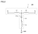
- Fig. 2 is a circuit diagram of a filter circuit 100 including the coil component 1 according to the first embodiment.
- the X-axis direction is the left-right direction of the coil component 1
- the Y-axis direction is the front-rear direction of the coil component 1
- the Z-axis direction is the up-down direction of the coil component 1.
- Coil component 1 is, for example, a transformer coil mounted in a filter circuit 100 used to reduce noise in power lines. As described below, coil component 1 magnetically couples two coils in order to cancel the parasitic inductance of a capacitor mounted in the filter circuit. Furthermore, coil component 1 employs a structure in which the terminals of the two coils are used to form a third coil.
- the coil component 1 includes a coil portion 2a (first coil) and a coil portion 3a (second coil) in a housing 4.
- the coil portion 2a is also referred to as coil L1
- the coil portion 3a is also referred to as coil L2.
- the coils L1 and L2 are formed from a metal plate, for example, copper or an alloy of copper and other metals.
- the coils L1 and L2 formed from the metal plate are covered with an insulating material (not shown).
- the insulating material covering the coils L1 and L2 is a resin such as polyimide imide or epoxy. Note that the insulating material does not need to cover all surfaces of the coils L1 and L2.
- the coil may be formed from multiple layers.
- the coil portion 2a has one end connected to a lead wire 2b (first lead wire) and the other end connected to a lead wire 2d (second lead wire). Furthermore, the lead wire 2b includes an electrode 2c that functions as an electrode, and the lead wire 2d includes an electrode 2e that functions as an electrode.
- the coil portion 2a and the lead wires 2b and 2d are formed as a single first conductor 2. Note that the lead wires 2b and 2d are also terminals extending from one end of the coil portion 2a, and are therefore also referred to as terminals 2b and 2d.
- the coil portion 3a has one end connected to a lead wire 3b (third lead wire) and the other end connected to a lead wire 3d (fourth lead wire). Furthermore, the lead wire 3b includes an electrode 3c that functions as an electrode, and the lead wire 3d includes an electrode 3e that functions as an electrode.
- the coil portion 3a and the lead wires 3b and 3d are formed as a single second conductor 3.
- the lead wires 3b and 3d are also terminals extending from one end of the coil portion 3a, and are therefore also referred to as terminals 3b and 3d.
- the first conductor 2 including the coil L1 and the second conductor 3 including the coil L2 are formed by bending a pattern punched out from a single metal plate.
- the bent portion between the coil L1 (coil portion 2a) and the lead wires 2b, 2d, and the bent portion between the electrodes 2c, 2e and the other areas of the lead wires 2b, 2d are formed by bending, and therefore have a substantially right-angle structure with a radius of curvature.
- the bent portion between the coil L2 (coil portion 3a) and the lead wires 3b, 3d, and the bent portion between the electrodes 3c, 3e and the other areas of the lead wires 3b, 3d are formed by bending, and therefore have a substantially right-angle structure with a radius of curvature. In this way, an arc with a certain radius is formed at the bent portion.
- the first conductor 2 and the second conductor 3 may be formed of one or more wires, and the wires may be bent in the same manner to form an arc with a certain radius at the bent portion.
- Coils L1 and L2 are arranged so that their openings overlap.
- Figure 1A shows an example in which the openings almost overlap, but as long as the openings are within the range of magnetic field coupling, they may be offset from each other, and it is sufficient that at least 50% of one opening overlaps.
- Coils L1 and L2 generate a magnetic field in coil L1 when a current flows from electrode 2c of first conductor 2 in the direction indicated by the arrow (clockwise), and a magnetic field in the same direction as the magnetic field of coil L1 is generated in coil L2 when a current flows from electrode 2e to coil L2 from electrode 3e of second conductor 3.
- Coils L1 and L2 are electrically connected by connecting the small gap between electrodes 2e and 3e with a connecting member (not shown), but electrodes 2e and 3e may also be connected by a mounting board without using a connecting member.
- Coil component 1 becomes a third coil L3 by flowing a current in the direction indicated by the arrow (counterclockwise) through the opening formed by coil portion 2a (coil L1), coil portion 3a (coil L2), lead wire 2d, electrode 2e, connection member 5, electrode 3e, and lead wire 3d, generating a magnetic field.
- the housing 4 is made of a molded resin for fixing the coils L1 and L2.
- the molded resin is made of one of epoxy resins with added silica filler, silicone resin, liquid crystal polymer, or various resins mixed with metal magnetic material.
- a rectangular parallelepiped shape is shown in FIG. 1A, as long as the second main surface, which is the mounting surface, and the coil surface are approximately parallel, the side surfaces may be inclined, and for example, the shape may be a trapezoid in which the area of the second main surface is larger than that of the first main surface.
- the filter circuit 100 is, for example, an EMI removal filter, and is a third-order T-type LC filter circuit.
- the electrode 2c is connected to a power source (not shown), and the electrode 3c is connected to a circuit (not shown) such as a DC/DC converter or a power supply module.
- the filter circuit 100 passes necessary components of the current flowing from the power source to the circuit and removes unnecessary components. Specifically, a direct current is passed through the filter circuit 100, and high-frequency noise contained in the direct current is dropped to GND through the capacitor C1.
- the capacitor C1 which is a capacitance element, has an equivalent series inductance ESL (La), which prevents high-frequency noise from passing through, and the noise removal performance is deteriorated.
- This filter circuit 100 uses a negative inductance generated in series in the capacitor C1 due to the mutual inductance generated by the magnetic coupling of the two coils to cancel the ESL (La) of the capacitor, thereby maintaining high noise removal performance.
- the filter circuit 100 will be described using a third-order T-type LC filter circuit, but coil components of a similar configuration can also be applied to a fifth-order T-type LC filter circuit or a higher-order T-type LC filter circuit.
- the filter circuit 100 includes a coil component 1 and a capacitor C1.
- the coil component 1 includes electrodes 2c, 3c, an intermediate terminal T (electrodes 2e, 3e, connecting member), a coil L1, and a coil L2.
- the capacitor C1 has one end connected to the intermediate terminal T and the other end connected to the GND wiring.
- the capacitor C1 may be a multilayer ceramic capacitor mainly made of BaTiO 3 (barium titanate), a multilayer ceramic capacitor mainly made of other materials, or another type of capacitor such as an aluminum electrolytic capacitor.
- the capacitor C1 has an inductor La as a parasitic inductance (equivalent series inductance (ESL)), and is equivalent to a circuit configuration in which the inductor La is connected in series to the capacitor C1a.
- the capacitor C1 may also be equivalent to a circuit configuration in which a parasitic resistance (equivalent series resistance (ESR)) is connected in series to the inductor La and the capacitor C1a.
- coils L1 and L2 are connected to the intermediate terminal T. Coils L1 and L2 are magnetically coupled and have mutual inductance. A negative inductance component of the same magnitude as the mutual inductance is generated between the intermediate terminal T and the capacitor C1. This negative inductance component can be used to cancel out the parasitic inductance (inductor La) of the capacitor C1, making the parasitic inductance component of the capacitor C1 appear smaller.
- the filter circuit 100 which is composed of the capacitor C1, coil L1, and coil L2, can cancel out the parasitic inductance of the capacitor C1 with the negative inductance component due to the mutual inductance between coils L1 and L2, thereby suppressing the decrease in the noise suppression effect in the high frequency band caused by the parasitic inductance of the capacitor C1 and improving the noise suppression effect of the filter circuit 100.
- coil component 1 instead of simply drawing out wiring from intermediate terminal T connecting coils L1 and L2 and connecting it to capacitor C1, as shown in FIG. 1A, a coil (coil L3) is formed using terminals 2d, 3d, and connecting members and connected to capacitor C1. Specifically, of terminals 2d and 3d, electrodes 2e and 3e on the second main surface are electrically connected to wiring on the board, and connected to capacitor C1 which is electrically connected to the same wiring.
- coil L3 itself, which is connected to capacitor C1 is also coupled as part of coils L1 and L2, and therefore contributes to the negative inductance component due to the mutual inductance between coils L1 and L2, and does not reduce the negative inductance component.
- the intermediate terminal T that connects coils L1 and L2 is a coil (coil L3) that is composed of terminals 2d, 3d, and connecting member 5, so the three coils L1 to L3 have a positive coupling coefficient.
- coil component 1 electrodes 2c and 3c are connected to the power line. Heat generated from the coil near electrodes 2c and 3c connected to the power line is dissipated through the power line. In contrast, when coil component 1 is used as a filter circuit, heat generated from the coil near electrodes 2e and 3e connected to the capacitor is not properly dissipated like the power line because it is connected to wiring that does not have sufficient heat dissipation measures, unlike the power line which has heat dissipation measures.
- the connecting member between electrode 2e and electrode 3e may be on the board to be mounted, not on coil component 1.
- the shortest distance of the drawers is defined as the shortest distance in the direction in which each drawer extends (Y-axis direction in the figure) on the second main surface.
- the drawers are spaced apart and opposed to each other in the Y-axis direction, but they may also be opposed to each other in the X-axis direction. In this case, the shortest distance in the extension direction of the drawers is also compared.
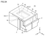
- Fig. 3A is a perspective view of a coil component 1A according to the second embodiment.
- Fig. 3B is an exploded view of the coil according to the second embodiment. Note that in the coil component 1A shown in the second embodiment, the same reference numerals are used for the same components as those in the coil component 1 according to the first embodiment, and detailed description thereof will not be repeated.
- the first conductor 2 has wires 2b and 2d drawn from the coil L1 out the rear surface of the housing 4, with wire 2b being arranged on the rear surface of the housing 4 and wire 2d being arranged from the rear surface to the right side of the housing 4.
- the second conductor 3 has wires 3b and 3d drawn from the coil L2 out the front surface of the housing 4, with wire 3b being arranged on the front surface of the housing 4 and wire 3d being arranged from the front surface to the right side of the housing 4.
- the area of the lead wires 2d and 3d is larger than that of the lead wires 2b and 3b.
- the area of the lead wires extending from the bent portion connected to the coil portion 2a or 3a to the second main surface when viewed in the thickness direction of the coil is the area of the lead wire. This allows the area for dissipating heat generated by the lead wires 2d and 3d to be large, thereby improving the heat dissipation performance of the coil component 1A.
- the cross-sectional area of the end portion of the lead wires 2d and 3d facing the second main surface is larger than the cross-sectional area of the end portion of the lead wires 2d and 3d facing the second main surface. This increases the area of connection between the lead wires 2d and 3d and the mounting board, improving the heat dissipation performance.
- the length in the extension direction may be changed, or the area may be changed by changing the width of the coil.
- the first conductor 2 is configured such that the lead wires 2b and 2d expand after the coil is closed at the lead wires 2b and 2d.
- the second conductor 3 is configured such that the lead wires 3b and 3d expand after the coil is closed at the lead wires 3b and 3d. This allows the coil component 1A to reduce the effects of parasitic inductance and parasitic capacitance of the electrode portion caused by the lead wires 2b and 2d, and the lead wires 3b and 3d being too close to each other.
- the positions of lead wires 2b, 2d, 3b, and 3d can be arranged as shown in FIG. 3A, which allows for improved freedom of wiring on the substrate on which it is mounted, and also allows for a larger area of the electrodes formed on the side of the housing, improving heat dissipation.
- the electrodes extending from lead wires 2b, 2d, 3b, and 3d may be arranged on the underside. Any of the multiple electrodes may be arranged on the underside and any may be arranged on the side. Note that, although the diagram shows them at right angles as a schematic diagram, the bent portion has an arc shape because it is formed by bending.
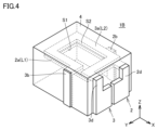
- Fig. 4 is a perspective view of a coil component 1B according to the third embodiment. Note that in the coil component 1B shown in the third embodiment, the same reference numerals are used for the same components as those in the coil component 1 according to the first embodiment, and detailed description thereof will not be repeated.
- the first conductor 2 has lead wire 2b from coil L1 drawn out from the rear surface of the housing 4, with the end of lead wire 2b located on the rear surface, lead wire 2d drawn out from the right side surface of the housing 4, with the end of lead wire 2d located on the right side surface of the housing 4.
- the second conductor 3 has lead wire 3b from coil L2 drawn out from the front surface of the housing 4, with the end of lead wire 3b located on the front surface of the housing 4, lead wire 3d drawn out from the right side surface of the housing 4, with the end of lead wire 3d located on the right side surface of the housing 4.
- the area of the lead wires 2d, 3d is larger than the area of the lead wires 2b, 3b. This allows a larger area for heat generated in the lead wires 2d and 3d to dissipate, improving the heat dissipation performance of the coil component 1B. Furthermore, the cross-sectional area of the ends of the lead wires 2d, 3d facing the second main surface is larger than the cross-sectional area of the ends of the lead wires 2d, 3d facing the second main surface. This increases the area of connection between the lead wires 2d and 3d and the mounting board, improving heat dissipation.
- the first conductor 2 is configured such that the lead wires 2b and 2d expand after the coil is closed at the lead wires 2b and 2d.
- the second conductor 3 is configured such that the lead wires 3b and 3d expand after the coil is closed at the lead wires 3b and 3d. This allows the coil component 1A to reduce the effects of parasitic inductance and parasitic capacitance of the electrode portion caused by the lead wires 2b and 2d, and the lead wires 3b and 3d being too close to each other.
- the positions of lead wires 2b, 2d, 3b, and 3d can be arranged as shown in FIG. 4, improving the degree of freedom of wiring on the substrate on which it is mounted.
- the electrodes extending from lead wires 2b, 2d, 3b, and 3d may be arranged on the underside. Any of the multiple electrodes may be arranged on the underside and any of the electrodes may be arranged on the side. Note that, although the diagram shows them at right angles as a schematic diagram, the bent portion has an arc shape because it is formed by bending.
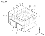
- Fig. 5A is a perspective view of a coil component 1C according to the fourth embodiment.
- Fig. 5B is an exploded view of the coil according to the fourth embodiment. Note that in the coil component 1C shown in the fourth embodiment, the same reference numerals are used for the same components as those in the coil component 1 according to the first embodiment, and detailed description thereof will not be repeated.
- the first conductor 2 has wires 2b and 2d drawn from the coil L1 out the left side of the housing 4, wire 2b arranged from the left side to the rear of the housing 4, and wire 2d arranged from the left side to the front of the housing 4.
- the second conductor 3 has wires 3b and 3d drawn from the coil L2 out the right side of the housing 4, wire 3b arranged from the right side to the rear of the housing 4, and wire 3d arranged from the right side to the front of the housing 4.
- most of the wires 2b, 2d, 3b, and 3d are embedded inside the housing 4, and only the portions of the wires near the ends that reach the second main surface are exposed from the housing 4.
- the area of the lead wires 2d, 3d is larger than the area of the lead wires 2b, 3b. This allows a larger area for heat generated in the lead wires 2d and 3d to dissipate, improving the heat dissipation performance of the coil component 1C.
- the cross-sectional area of the ends of the lead wires 2d, 3d is larger than the cross-sectional area of the ends of the lead wires 2b, 3b. This increases the area of connection between the lead wires 2d and 3d and the mounting board, improving heat dissipation.
- the first conductor 2 is configured such that the lead wires 2b and 2d expand after the coil is closed at the lead wires 2b and 2d.
- the second conductor 3 is configured such that the lead wires 3b and 3d expand after the coil is closed at the lead wires 3b and 3d. This allows the coil component 1A to reduce the effects of parasitic inductance and parasitic capacitance of the electrode portion caused by the lead wires 2b and 2d, and the lead wires 3b and 3d being too close to each other.
- the positions of lead wires 2b, 2d, 3b, and 3d can be arranged as shown in FIG. 5A, improving the degree of freedom of wiring on the substrate on which it is mounted.
- the electrodes extending from lead wires 2b, 2d, 3b, and 3d may be arranged on the underside. Any one of the multiple electrodes may be arranged on the underside and any one on the side. Note that, although the diagram shows them at right angles as a schematic diagram, the bent portion has an arc shape because it is formed by bending.
- Fig. 6A is a perspective view of a coil component 1D according to the fifth embodiment.
- Fig. 6B is an exploded view of the coil according to the second embodiment. Note that in the coil component 1D shown in the fifth embodiment, the same reference numerals are used for the same components as those in the coil component 1 according to the first embodiment, and detailed description thereof will not be repeated.
- the first conductor 2 has lead wire 2b from coil L1 drawn out from the rear surface of the housing 4 and lead wire 2b is arranged on the rear surface of the housing 4, lead wire 2d drawn out from the left side surface of the housing 4 and lead wire 2d is arranged on the left side surface of the housing 4.
- the second conductor 3 has lead wire 3b drawn out from coil L2 from the right side surface of the housing 4 and lead wire 3b is arranged on the right side surface of the housing 4, lead wire 3d drawn out from the front surface of the housing 4 and lead wire 3d is arranged on the front surface of the housing 4.
- the area of the lead wires 2d, 3d is larger than the area of the lead wires 2b, 3b. This allows a larger area for heat generated in the lead wires 2d and 3d to dissipate, improving the heat dissipation performance of the coil component 1D.
- the cross-sectional area of the ends of the lead wires 2d, 3d is larger than the cross-sectional area of the ends of the lead wires 2b, 3b. This increases the area of connection between the lead wires 2d and 3d and the mounting board, improving heat dissipation.
- by forming one terminal on each side as shown in Figure 6A it is possible to accommodate miniaturization and the width of the terminals can also be made wider.
- the first conductor 2 is configured such that the lead wires 2b and 2d expand after the coil is closed at the lead wires 2b and 2d.
- the second conductor 3 is configured such that the lead wires 3b and 3d expand after the coil is closed at the lead wires 3b and 3d. This allows the coil component 1A to reduce the effects of parasitic inductance and parasitic capacitance of the electrode portion caused by the lead wires 2b and 2d, and the lead wires 3b and 3d being too close to each other.
- the positions of lead wires 2b, 2d, 3b, and 3d can be arranged as shown in FIG. 6A, improving the degree of freedom of wiring on the substrate on which it is mounted.
- the electrodes extending from lead wires 2b, 2d, 3b, and 3d may be arranged on the underside. Any one of the multiple electrodes may be arranged on the underside and any one on the side. Note that, although the diagram shows a schematic diagram with a right angle, the bent portion has an arc shape because it is formed by bending.
- Fig. 7 is a perspective view of a coil component 1E according to the sixth embodiment. Note that in the coil component 1E shown in the sixth embodiment, the same reference numerals are used for the same components as those in the coil component 1 according to the first embodiment, and detailed description thereof will not be repeated.
- connection member 5 is disposed, which electrically connects electrodes 2e and 3e.
- Connection member 5 is T-shaped with its tip extending from electrodes 2e and 3e toward the left side surface of housing 4.
- the area of electrodes 2e and 3e is the same as that of electrodes 2c and 3c, but the connecting member 5 provides a larger area for dissipating heat generated by electrodes 2e and 3e. This improves the heat dissipation performance of coil component 1E.
- the area of at least one of the electrodes 2e, 3e, and the connecting member 5 may be larger than the area of the electrodes 2c and 3c.
- Coils L1 and L2 may not be a single metal plate, but may have a multi-layer structure in which multiple layers are stacked to form a coil component.
- the housing 4 has been described as having a rectangular parallelepiped shape.
- the housing 4 may have any shape, for example, a cylindrical shape.
- the coil component of the present disclosure includes a housing having a pair of first and second main surfaces facing each other and four side surfaces connecting the first and second main surfaces, a first coil disposed inside the housing and disposed substantially parallel to the first main surface, and a second coil disposed inside the housing such that an opening of the first coil overlaps an opening of the second coil when viewed from the direction of the first main surface.
- the coil component includes a first lead wire and a second lead wire connected to ends of the first coil, respectively, and a third lead wire and a fourth lead wire connected to ends of the second coil, respectively.
- the second lead wire and the fourth lead wire are electrically connected. At least one of the second lead wire and the fourth lead wire has an area larger than the areas of the first lead wire and the third lead wire.
- the second and fourth drawers are electrically connected, and the area of at least one of the second and fourth drawers is larger than the area of the first and third drawers, thereby improving heat dissipation performance.
- the coil component of the present disclosure includes a housing having a pair of first and second main surfaces facing each other and four side surfaces connecting the first and second main surfaces, a first coil disposed inside the housing and disposed substantially parallel to the first main surfaces, and a second coil disposed inside the housing such that an opening of the first coil overlaps with an opening when viewed from the direction of the first main surfaces.
- the coil component includes a first lead wire and a second lead wire respectively connected to ends of the first coil, and a third lead wire and a fourth lead wire respectively connected to ends of the second coil. The shortest distance between the first lead wire and the third lead wire is farther than the shortest distance between the second lead wire and the fourth lead wire.
- the coil component disclosed herein can improve the heat dissipation performance of the coil component by shortening the heat generating area between the second and fourth drawers while ensuring a sufficient distance between the first and third drawers to prevent a short circuit when mounted on a board.
- the shortest distance between the first and third drawers is at a position on the second main surface or on the side closest to the second main surface
- the shortest distance between the second and fourth drawers is at a position on the second main surface or on the side closest to the second main surface. This improves the heat dissipation performance at a position close to the second main surface.
- connection member disposed on the second main surface and electrically connecting the second lead wire and the fourth lead wire. This allows heat to be dissipated in the connection member, thereby improving the heat dissipation performance of the coil component.
- the filter circuit of the present disclosure includes a coil component according to any one of (1) to (12) and a capacitor electrically connected to the second and fourth lead wires. This makes it possible to provide a filter circuit that incorporates a coil component with high heat dissipation performance.
Landscapes
- Engineering & Computer Science (AREA)
- Power Engineering (AREA)
- Coils Or Transformers For Communication (AREA)
Priority Applications (1)
| Application Number | Priority Date | Filing Date | Title |
|---|---|---|---|
| JP2024571614A JPWO2024154388A1 (https=) | 2023-01-19 | 2023-09-26 |
Applications Claiming Priority (2)
| Application Number | Priority Date | Filing Date | Title |
|---|---|---|---|
| JP2023-006741 | 2023-01-19 | ||
| JP2023006741 | 2023-01-19 |
Publications (1)
| Publication Number | Publication Date |
|---|---|
| WO2024154388A1 true WO2024154388A1 (ja) | 2024-07-25 |
Family
ID=91955544
Family Applications (1)
| Application Number | Title | Priority Date | Filing Date |
|---|---|---|---|
| PCT/JP2023/034862 Ceased WO2024154388A1 (ja) | 2023-01-19 | 2023-09-26 | コイル部品、およびフィルタ回路 |
Country Status (2)
| Country | Link |
|---|---|
| JP (1) | JPWO2024154388A1 (https=) |
| WO (1) | WO2024154388A1 (https=) |
Citations (2)
| Publication number | Priority date | Publication date | Assignee | Title |
|---|---|---|---|---|
| JP2012526386A (ja) * | 2009-05-04 | 2012-10-25 | クーパー テクノロジーズ カンパニー | 磁気部品とその製造方法 |
| WO2022070888A1 (ja) * | 2020-10-01 | 2022-04-07 | 株式会社村田製作所 | コイル部品、これを含むフィルタ回路、および電子機器 |
-
2023
- 2023-09-26 JP JP2024571614A patent/JPWO2024154388A1/ja active Pending
- 2023-09-26 WO PCT/JP2023/034862 patent/WO2024154388A1/ja not_active Ceased
Patent Citations (2)
| Publication number | Priority date | Publication date | Assignee | Title |
|---|---|---|---|---|
| JP2012526386A (ja) * | 2009-05-04 | 2012-10-25 | クーパー テクノロジーズ カンパニー | 磁気部品とその製造方法 |
| WO2022070888A1 (ja) * | 2020-10-01 | 2022-04-07 | 株式会社村田製作所 | コイル部品、これを含むフィルタ回路、および電子機器 |
Also Published As
| Publication number | Publication date |
|---|---|
| JPWO2024154388A1 (https=) | 2024-07-25 |
Similar Documents
| Publication | Publication Date | Title |
|---|---|---|
| US7280342B1 (en) | Low inductance high ESR capacitor | |
| US12355416B2 (en) | Coil component, filter circuit including the coil component, and electronic device | |
| CN219164535U (zh) | 滤波器电路以及包含该滤波器电路的电源装置 | |
| US20240428985A1 (en) | Circuit device and filter circuit | |
| US11870412B2 (en) | Multilayer substrate, circuit device, and filter circuit substrate | |
| JP2018019512A (ja) | 出力ノイズ低減装置 | |
| US10284164B2 (en) | Circuit substrate, filter circuit, and capacitance element | |
| WO2020066192A1 (ja) | 電子制御装置 | |
| WO2024154388A1 (ja) | コイル部品、およびフィルタ回路 | |
| WO2024247619A1 (ja) | コイル部品、およびフィルタ回路 | |
| US20240297631A1 (en) | Circuit device | |
| JP7750436B2 (ja) | コイル部品、これを含むフィルタ回路 | |
| WO2024154391A1 (ja) | コイル部品、およびフィルタ回路 | |
| WO2024166971A1 (ja) | 回路装置、および回路基板 | |
| JP2024030719A (ja) | 電気的ノイズ抑制回路及びそれを備えたブラシ付きdcモータ | |
| WO2025047045A1 (ja) | コイル部品、これを含む回路装置 | |
| WO2025083974A1 (ja) | コイル部品、およびフィルタ回路 | |
| JP4379107B2 (ja) | 電子部品 | |
| WO2026048259A1 (ja) | コイル部品、これを含む電子機器 | |
| WO2025062805A1 (ja) | コイル部品、およびフィルタ回路 | |
| JP7130174B2 (ja) | フィルタ回路 | |
| US20250192746A1 (en) | Filter circuit | |
| JP7764950B2 (ja) | ノイズ低減機能部品を備えたスイッチング電源装置 | |
| JP7677863B2 (ja) | コンデンサ装置 | |
| JP4985852B2 (ja) | 実装型電子回路モジュール |
Legal Events
| Date | Code | Title | Description |
|---|---|---|---|
| 121 | Ep: the epo has been informed by wipo that ep was designated in this application |
Ref document number: 23917600 Country of ref document: EP Kind code of ref document: A1 |
|
| WWE | Wipo information: entry into national phase |
Ref document number: 2024571614 Country of ref document: JP |
|
| NENP | Non-entry into the national phase |
Ref country code: DE |
|
| 122 | Ep: pct application non-entry in european phase |
Ref document number: 23917600 Country of ref document: EP Kind code of ref document: A1 |