WO2024154372A1 - 圧電振動素子、圧電振動子及び圧電発振器 - Google Patents
圧電振動素子、圧電振動子及び圧電発振器 Download PDFInfo
- Publication number
- WO2024154372A1 WO2024154372A1 PCT/JP2023/028449 JP2023028449W WO2024154372A1 WO 2024154372 A1 WO2024154372 A1 WO 2024154372A1 JP 2023028449 W JP2023028449 W JP 2023028449W WO 2024154372 A1 WO2024154372 A1 WO 2024154372A1
- Authority
- WO
- WIPO (PCT)
- Prior art keywords
- excitation electrode
- vibration element
- hole
- har
- element according
- Prior art date
Links
- 230000010355 oscillation Effects 0.000 title description 4
- 230000005284 excitation Effects 0.000 claims abstract description 296
- 230000000149 penetrating effect Effects 0.000 claims abstract description 5
- 239000013078 crystal Substances 0.000 claims description 119
- VYPSYNLAJGMNEJ-UHFFFAOYSA-N silicon dioxide Inorganic materials O=[Si]=O VYPSYNLAJGMNEJ-UHFFFAOYSA-N 0.000 claims description 118
- 239000010453 quartz Substances 0.000 claims description 114
- 239000000758 substrate Substances 0.000 claims description 31
- 239000000463 material Substances 0.000 claims description 13
- 229910052782 aluminium Inorganic materials 0.000 claims description 9
- XAGFODPZIPBFFR-UHFFFAOYSA-N aluminium Chemical group [Al] XAGFODPZIPBFFR-UHFFFAOYSA-N 0.000 claims description 9
- 230000008878 coupling Effects 0.000 description 123
- 238000010168 coupling process Methods 0.000 description 123
- 238000005859 coupling reaction Methods 0.000 description 123
- 235000012239 silicon dioxide Nutrition 0.000 description 110
- 230000000052 comparative effect Effects 0.000 description 22
- 238000004088 simulation Methods 0.000 description 22
- 239000010410 layer Substances 0.000 description 21
- 230000000694 effects Effects 0.000 description 14
- 238000000605 extraction Methods 0.000 description 14
- 239000000919 ceramic Substances 0.000 description 9
- 239000011521 glass Substances 0.000 description 7
- PXHVJJICTQNCMI-UHFFFAOYSA-N Nickel Chemical compound [Ni] PXHVJJICTQNCMI-UHFFFAOYSA-N 0.000 description 6
- 229910016570 AlCu Inorganic materials 0.000 description 5
- 229910000881 Cu alloy Inorganic materials 0.000 description 5
- WPPDFTBPZNZZRP-UHFFFAOYSA-N aluminum copper Chemical compound [Al].[Cu] WPPDFTBPZNZZRP-UHFFFAOYSA-N 0.000 description 5
- 239000000853 adhesive Substances 0.000 description 4
- 230000001070 adhesive effect Effects 0.000 description 4
- 229910045601 alloy Inorganic materials 0.000 description 4
- 239000000956 alloy Substances 0.000 description 4
- 238000010586 diagram Methods 0.000 description 4
- 239000010931 gold Substances 0.000 description 4
- 239000004593 Epoxy Substances 0.000 description 3
- XUIMIQQOPSSXEZ-UHFFFAOYSA-N Silicon Chemical compound [Si] XUIMIQQOPSSXEZ-UHFFFAOYSA-N 0.000 description 3
- 230000007423 decrease Effects 0.000 description 3
- 239000007772 electrode material Substances 0.000 description 3
- 238000012986 modification Methods 0.000 description 3
- 230000004048 modification Effects 0.000 description 3
- 229910052710 silicon Inorganic materials 0.000 description 3
- 239000010703 silicon Substances 0.000 description 3
- 230000035882 stress Effects 0.000 description 3
- XEEYBQQBJWHFJM-UHFFFAOYSA-N Iron Chemical compound [Fe] XEEYBQQBJWHFJM-UHFFFAOYSA-N 0.000 description 2
- 229910017709 Ni Co Inorganic materials 0.000 description 2
- 229910003267 Ni-Co Inorganic materials 0.000 description 2
- 229910003262 Ni‐Co Inorganic materials 0.000 description 2
- 238000006243 chemical reaction Methods 0.000 description 2
- 239000011651 chromium Substances 0.000 description 2
- 239000010949 copper Substances 0.000 description 2
- PCHJSUWPFVWCPO-UHFFFAOYSA-N gold Chemical compound [Au] PCHJSUWPFVWCPO-UHFFFAOYSA-N 0.000 description 2
- 229910052737 gold Inorganic materials 0.000 description 2
- 229910052451 lead zirconate titanate Inorganic materials 0.000 description 2
- 229910052751 metal Inorganic materials 0.000 description 2
- 239000002184 metal Substances 0.000 description 2
- 229910052759 nickel Inorganic materials 0.000 description 2
- 230000003071 parasitic effect Effects 0.000 description 2
- 229910052814 silicon oxide Inorganic materials 0.000 description 2
- 229910000679 solder Inorganic materials 0.000 description 2
- 230000008646 thermal stress Effects 0.000 description 2
- 239000010936 titanium Substances 0.000 description 2
- QNRATNLHPGXHMA-XZHTYLCXSA-N (r)-(6-ethoxyquinolin-4-yl)-[(2s,4s,5r)-5-ethyl-1-azabicyclo[2.2.2]octan-2-yl]methanol;hydrochloride Chemical group Cl.C([C@H]([C@H](C1)CC)C2)CN1[C@@H]2[C@H](O)C1=CC=NC2=CC=C(OCC)C=C21 QNRATNLHPGXHMA-XZHTYLCXSA-N 0.000 description 1
- WSMQKESQZFQMFW-UHFFFAOYSA-N 5-methyl-pyrazole-3-carboxylic acid Chemical compound CC1=CC(C(O)=O)=NN1 WSMQKESQZFQMFW-UHFFFAOYSA-N 0.000 description 1
- 229920000178 Acrylic resin Polymers 0.000 description 1
- OYPRJOBELJOOCE-UHFFFAOYSA-N Calcium Chemical compound [Ca] OYPRJOBELJOOCE-UHFFFAOYSA-N 0.000 description 1
- VYZAMTAEIAYCRO-UHFFFAOYSA-N Chromium Chemical compound [Cr] VYZAMTAEIAYCRO-UHFFFAOYSA-N 0.000 description 1
- RYGMFSIKBFXOCR-UHFFFAOYSA-N Copper Chemical compound [Cu] RYGMFSIKBFXOCR-UHFFFAOYSA-N 0.000 description 1
- JOYRKODLDBILNP-UHFFFAOYSA-N Ethyl urethane Chemical compound CCOC(N)=O JOYRKODLDBILNP-UHFFFAOYSA-N 0.000 description 1
- ZOKXTWBITQBERF-UHFFFAOYSA-N Molybdenum Chemical compound [Mo] ZOKXTWBITQBERF-UHFFFAOYSA-N 0.000 description 1
- 229910052581 Si3N4 Inorganic materials 0.000 description 1
- 229910004298 SiO 2 Inorganic materials 0.000 description 1
- RTAQQCXQSZGOHL-UHFFFAOYSA-N Titanium Chemical compound [Ti] RTAQQCXQSZGOHL-UHFFFAOYSA-N 0.000 description 1
- NIXOWILDQLNWCW-UHFFFAOYSA-N acrylic acid group Chemical group C(C=C)(=O)O NIXOWILDQLNWCW-UHFFFAOYSA-N 0.000 description 1
- 230000032683 aging Effects 0.000 description 1
- 229910052791 calcium Inorganic materials 0.000 description 1
- 239000011575 calcium Substances 0.000 description 1
- 239000003990 capacitor Substances 0.000 description 1
- 239000004568 cement Substances 0.000 description 1
- 229910052804 chromium Inorganic materials 0.000 description 1
- 239000010941 cobalt Substances 0.000 description 1
- 229910017052 cobalt Inorganic materials 0.000 description 1
- GUTLYIVDDKVIGB-UHFFFAOYSA-N cobalt atom Chemical compound [Co] GUTLYIVDDKVIGB-UHFFFAOYSA-N 0.000 description 1
- 238000004891 communication Methods 0.000 description 1
- 239000004020 conductor Substances 0.000 description 1
- 229910052802 copper Inorganic materials 0.000 description 1
- PMHQVHHXPFUNSP-UHFFFAOYSA-M copper(1+);methylsulfanylmethane;bromide Chemical compound Br[Cu].CSC PMHQVHHXPFUNSP-UHFFFAOYSA-M 0.000 description 1
- 239000006023 eutectic alloy Substances 0.000 description 1
- 239000007789 gas Substances 0.000 description 1
- JVPLOXQKFGYFMN-UHFFFAOYSA-N gold tin Chemical compound [Sn].[Au] JVPLOXQKFGYFMN-UHFFFAOYSA-N 0.000 description 1
- 239000011261 inert gas Substances 0.000 description 1
- 230000001678 irradiating effect Effects 0.000 description 1
- 229910000833 kovar Inorganic materials 0.000 description 1
- HFGPZNIAWCZYJU-UHFFFAOYSA-N lead zirconate titanate Chemical compound [O-2].[O-2].[O-2].[O-2].[O-2].[Ti+4].[Zr+4].[Pb+2] HFGPZNIAWCZYJU-UHFFFAOYSA-N 0.000 description 1
- ZPPSOOVFTBGHBI-UHFFFAOYSA-N lead(2+);oxido(oxo)borane Chemical compound [Pb+2].[O-]B=O.[O-]B=O ZPPSOOVFTBGHBI-UHFFFAOYSA-N 0.000 description 1
- GQYHUHYESMUTHG-UHFFFAOYSA-N lithium niobate Chemical compound [Li+].[O-][Nb](=O)=O GQYHUHYESMUTHG-UHFFFAOYSA-N 0.000 description 1
- 230000008018 melting Effects 0.000 description 1
- 238000002844 melting Methods 0.000 description 1
- 239000007769 metal material Substances 0.000 description 1
- 238000010295 mobile communication Methods 0.000 description 1
- 229910052750 molybdenum Inorganic materials 0.000 description 1
- 239000011733 molybdenum Substances 0.000 description 1
- 230000003287 optical effect Effects 0.000 description 1
- 235000019353 potassium silicate Nutrition 0.000 description 1
- 238000007789 sealing Methods 0.000 description 1
- 239000000377 silicon dioxide Substances 0.000 description 1
- HQVNEWCFYHHQES-UHFFFAOYSA-N silicon nitride Chemical compound N12[Si]34N5[Si]62N3[Si]51N64 HQVNEWCFYHHQES-UHFFFAOYSA-N 0.000 description 1
- 229920002050 silicone resin Polymers 0.000 description 1
- 239000002356 single layer Substances 0.000 description 1
- NTHWMYGWWRZVTN-UHFFFAOYSA-N sodium silicate Chemical compound [Na+].[Na+].[O-][Si]([O-])=O NTHWMYGWWRZVTN-UHFFFAOYSA-N 0.000 description 1
- 239000000126 substance Substances 0.000 description 1
- 239000002344 surface layer Substances 0.000 description 1
- 229920002803 thermoplastic polyurethane Polymers 0.000 description 1
- QUBMWJKTLKIJNN-UHFFFAOYSA-B tin(4+);tetraphosphate Chemical compound [Sn+4].[Sn+4].[Sn+4].[O-]P([O-])([O-])=O.[O-]P([O-])([O-])=O.[O-]P([O-])([O-])=O.[O-]P([O-])([O-])=O QUBMWJKTLKIJNN-UHFFFAOYSA-B 0.000 description 1
- 229910052719 titanium Inorganic materials 0.000 description 1
- 125000000391 vinyl group Chemical group [H]C([*])=C([H])[H] 0.000 description 1
- 229920002554 vinyl polymer Polymers 0.000 description 1
- 238000003466 welding Methods 0.000 description 1
Images


Classifications
-
- H—ELECTRICITY
- H03—ELECTRONIC CIRCUITRY
- H03B—GENERATION OF OSCILLATIONS, DIRECTLY OR BY FREQUENCY-CHANGING, BY CIRCUITS EMPLOYING ACTIVE ELEMENTS WHICH OPERATE IN A NON-SWITCHING MANNER; GENERATION OF NOISE BY SUCH CIRCUITS
- H03B5/00—Generation of oscillations using amplifier with regenerative feedback from output to input
- H03B5/30—Generation of oscillations using amplifier with regenerative feedback from output to input with frequency-determining element being electromechanical resonator
- H03B5/32—Generation of oscillations using amplifier with regenerative feedback from output to input with frequency-determining element being electromechanical resonator being a piezoelectric resonator
-
- H—ELECTRICITY
- H03—ELECTRONIC CIRCUITRY
- H03H—IMPEDANCE NETWORKS, e.g. RESONANT CIRCUITS; RESONATORS
- H03H9/00—Networks comprising electromechanical or electro-acoustic elements; Electromechanical resonators
- H03H9/15—Constructional features of resonators consisting of piezoelectric or electrostrictive material
- H03H9/17—Constructional features of resonators consisting of piezoelectric or electrostrictive material having a single resonator
- H03H9/19—Constructional features of resonators consisting of piezoelectric or electrostrictive material having a single resonator consisting of quartz
Definitions
- the present invention relates to a piezoelectric vibration element, a piezoelectric vibrator, and a piezoelectric oscillator.
- a piezoelectric vibration element comprises a piezoelectric piece having a main surface extending in a first direction and a second direction intersecting the first direction and having a thickness in a third direction intersecting the first direction and the second direction, and an excitation electrode provided on the main surface, where the dimension of the excitation electrode along the first direction is Le1 and the dimension of the piezoelectric piece along the third direction is Tq, the relationship 45 ⁇ Le1/Tq ⁇ 120 holds, and a first hole portion penetrating the excitation electrode along the third direction is formed in the center of the excitation electrode in the first direction.
- the present invention provides a piezoelectric vibration element, a piezoelectric vibrator, and a piezoelectric oscillator that can improve the electromechanical coupling coefficient.
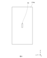
- FIG. 1 is a cross-sectional view of a crystal oscillator according to a first embodiment.
- 1 is a cross-sectional view of a quartz crystal resonator according to a first embodiment.
- FIG. 1 is a plan view of a quartz crystal vibration element according to a first embodiment.
- FIG. 2 is a plan view of a first excitation electrode according to the first embodiment.
- FIG. 2 is a cross-sectional view of a vibration section according to the first embodiment.
- FIG. 11 is a plan view of a first excitation electrode according to a second embodiment.
- FIG. 11 is a plan view of a first excitation electrode according to a third embodiment.
- FIG. 13 is a plan view of a first excitation electrode according to a fourth embodiment.
- FIG. 13 is a plan view of a first excitation electrode according to a fifth embodiment.
- FIG. 13 is a plan view of a first excitation electrode according to a sixth embodiment.
- FIG. 23 is a plan view of a first excitation electrode according to the seventh embodiment.
- FIG. 23 is a plan view of a first excitation electrode according to the eighth embodiment.
- FIG. 13 is a plan view of a first excitation electrode according to the 9th embodiment.
- FIG. 11 is a diagram showing a simulation result in the first embodiment. 11 is a graph showing the influence of the shape and size of a first hole in a rectangular first excitation electrode. 11 is a graph showing the influence of the shape and size of a first hole in a rectangular first excitation electrode.
- an orthogonal coordinate system consisting of the X-axis, Y'-axis, and Z'-axis may be conveniently attached to each drawing.
- the X-axis, Y'-axis, and Z'-axis correspond to each other in each drawing.
- the X-axis, Y'-axis, and Z'-axis each correspond to the crystallographic axes of the quartz piece 11, which will be described later.
- the X-axis corresponds to the electrical axis (polarity axis) of the quartz
- the Y-axis corresponds to the mechanical axis of the quartz
- the Z-axis corresponds to the optical axis of the quartz.
- the direction parallel to the X-axis is referred to as the "X-axis direction”
- the direction parallel to the Y'-axis is referred to as the "Y'-axis direction”
- the direction parallel to the Z'-axis is referred to as the "Z'-axis direction”.
- the directions of the tips of the arrows on the X-axis, Y'-axis, and Z'-axis are referred to as "positive” or "+ (plus)”, and the directions opposite the arrows are referred to as "negative” or "- (minus)".
- the +Y'-axis direction is described as the upward direction
- the -Y'-axis direction is described as the downward direction
- the up-down orientation of the quartz resonator element 10, the quartz resonator 1, and the quartz oscillator 100 is not limited to this.
- the plane specified by the X-axis and Z'-axis is referred to as the Z'X plane, and the same applies to the planes specified by the other axes.
- FIG. 1 is a cross-sectional view of the crystal oscillator according to the first embodiment.
- a crystal oscillator (XO: Crystal Oscillator) equipped with a crystal resonator (Quartz Crystal Resonator Unit) is used as an example of a piezoelectric oscillator.
- a crystal resonator (Quartz Crystal Resonator Unit) equipped with a crystal vibration element (Quartz Crystal Resonator) is used as an example of a piezoelectric vibrator.
- a crystal vibration element equipped with a crystal piece (Quartz Crystal Element) is used as an example of a piezoelectric vibration element.
- a crystal piece is a type of piezoelectric material (piezoelectric piece) that vibrates in response to an applied voltage.
- the quartz crystal unit 1 and electronic components 156 are housed in a space formed between the mounting substrate 130 and the lid 140.
- the space formed by the mounting substrate 130 and the lid 140 is, for example, hermetically sealed. This space may be hermetically sealed in a vacuum state, or may be hermetically sealed when filled with a gas such as an inert gas.
- the mounting board 130 is a flat circuit board.
- the mounting board 130 is configured to include, for example, a glass epoxy board and a wiring layer patterned on the glass epoxy board.
- the quartz crystal oscillator 1 is provided on one surface of the mounting substrate 130 (the upper surface in FIG. 1). More specifically, the quartz crystal oscillator 1 is electrically connected to the wiring layer of the mounting substrate 130 by a bonding wire 166. The quartz crystal oscillator 1 and the wiring layer of the mounting substrate 130 are also joined by solder 153. As a result, the quartz crystal oscillator 1 is sealed in the space formed between the mounting substrate 130 and the lid 140.
- the lid 140 includes a bottomed opening that is open on one side (the lower side in FIG. 1).
- the lid 140 includes a flat top wall portion, a side wall portion that extends from the outer edge of the top wall portion toward the mounting substrate 130, and a flange portion that extends outward from the tip of the side wall portion.
- the flange portion is bonded to one surface of the mounting substrate 130 (the upper surface in FIG. 1). This allows the crystal unit 1 bonded to the mounting substrate 130 to be housed inside the lid 140.
- the lid 140 is made of a metal material and is formed, for example, by drawing a metal plate.
- the electronic component 156 is provided on one surface (the upper surface in FIG. 1 ) of the mounting board 130. More specifically, the wiring layer of the mounting board 130 and the electronic component 156 are joined by solder 153. In this way, the electronic component 156 is mounted on the mounting board 130.
- the electronic component 156 is electrically connected to the crystal unit 1 through the wiring layer of the mounting board 130.
- the electronic component 156 includes, for example, a capacitor and an IC chip.
- the electronic component 156 is, for example, a part of an oscillation circuit that oscillates the crystal unit 1, or a part of a temperature compensation circuit that compensates for the temperature characteristics of the crystal unit 1.
- the crystal oscillator 100 is sometimes called a temperature compensated crystal oscillator (TCXO).
- Fig. 2 is a cross-sectional view of a quartz crystal resonator according to the first embodiment.
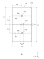
- Fig. 3 is a plan view of a quartz crystal resonator element according to the first embodiment.
- Fig. 4 is a plan view of a first excitation electrode according to the first embodiment.
- Fig. 5 is a cross-sectional view of a vibration part according to the first embodiment. Note that Fig. 2 shows a cross section parallel to the Y'Z' plane along line II-II shown in Fig. 3. Fig. 5 shows a cross section parallel to the Y'Z' plane along line V-V shown in Fig. 3.
- the quartz crystal oscillator 1 comprises a quartz crystal oscillator element 10, a top cover 20, a joint 30, an insulating layer 40, and a support substrate 50.
- the insulating layer 40 and the support substrate 50 are an example of a "first cover member,” and the top cover 20 is an example of a "second cover member.”
- the quartz crystal element 10 is an electromechanical energy conversion element that converts electrical energy into mechanical energy and vice versa by the piezoelectric effect.
- the main mode frequency of the quartz crystal element 10 is, for example, in the GHz band, for example, about 1.0 GHz to 2.0 GHz, for example, about 1.45 GHz.
- the inharmonic mode frequency of the quartz crystal element 10 exists, for example, within a range of about 1% of the main mode frequency.
- the quartz crystal piece 11 has an upper surface 12a and a lower surface 12b that face each other.
- the upper surface 12a is located on the side that faces the upper cover 20.
- the lower surface 12b is located on the side that faces the support substrate 50.
- the upper surface 12a and the lower surface 12b correspond to a pair of main surfaces of the quartz crystal piece 11.
- the quartz piece 11 is, for example, an AT-cut quartz crystal.
- An AT-cut quartz crystal is formed so that the XZ' plane is the main surface and the thickness is in the direction parallel to the Y' axis.
- the shape of the quartz piece 11 (hereinafter simply referred to as "plan view") is rectangular with long sides extending in the Z'-axis direction and short sides extending in the X-axis direction.
- the quartz piece 11 also has a thickness in the Y'-axis direction.
- the quartz piece 11 is in the shape of a flat plate with a uniform thickness.
- the planar shape of the quartz piece is not limited to the above, and may be a rectangle with a short side extending in the Z'-axis direction and a long side extending in the X-axis direction.
- the planar shape of the quartz piece may be a polygon, a circle, an ellipse, or a combination of these.
- the quartz piece is not limited to a flat plate, and may have a so-called mesa structure in which the thickness of the portion overlapping the first excitation electrode 14a and the second excitation electrode 14b is greater than the surrounding thickness.
- the quartz piece may have a so-called inverted mesa structure in which the thickness of the portion overlapping the first excitation electrode 14a and the second excitation electrode 14b is smaller than the surrounding thickness.
- the thickness of the quartz piece When the thickness of the quartz piece is changed partially, it may be a convex structure in which the amount of change in thickness changes continuously, or a bevel structure in which the amount of change in thickness changes discontinuously.
- the quartz crystal vibration element 10 using the AT-cut quartz crystal piece 11 has high frequency stability over a wide temperature range.
- the AT-cut quartz crystal vibration element has excellent aging characteristics and can be manufactured at low cost.
- the AT-cut quartz crystal vibration element uses the thickness shear vibration mode as its main vibration.
- the cut angle of the quartz piece is not limited to the above.
- the rotation angle of the Y'-axis and Z'-axis in the AT-cut quartz piece 11 may be tilted in the range of -5 degrees or more and +15 degrees or less from 35 degrees 15 minutes.
- the cut angle of the quartz piece may also be a different cut other than the AT cut, such as a BT cut, a GT cut, or an SC cut.
- the quartz crystal piece 11 includes a vibrating portion 11A, an opening 11B, and a holding portion 11C.
- the vibrating portion 11A of the quartz blank 11 vibrates at a predetermined resonant frequency with the thickness-shear vibration mode as the main vibration.
- the opening 11B of the quartz blank 11 is an opening formed to surround the vibrating portion 11A when the top surface 12a is viewed in plan.
- the opening 11B penetrates the thickness direction of the quartz blank 11 parallel to the Z' axis direction and communicates with a hollow portion 41 described later.
- the opening 11B is formed so that the vibrating portion 11A and the holding portion 11C are separated by, for example, about 10 ⁇ m.
- the holding portion 11C of the quartz blank 11 holds the end of the vibrating portion 11A (the lower end in FIG. 2).
- the holding portion 11C is connected, for example, to the side of the vibrating portion 11A on the negative side of the X-axis.
- the first excitation electrode 14a and the second excitation electrode 14b apply an alternating voltage to the vibration part 11A to excite the vibration part 11A.
- the first excitation electrode 14a and the second excitation electrode 14b are provided in the center of the vibration part 11A.
- the first excitation electrode 14a is provided on the upper surface 12a, and the second excitation electrode 14b is provided on the lower surface 12b.
- the first excitation electrode 14a and the second excitation electrode 14b face each other in the Y'-axis direction with the vibration part 11A in between.
- the planar shape of the first excitation electrode 14a is a rectangle with long sides extending in the Z'-axis direction and short sides extending in the X-axis direction.
- the first excitation electrode 14a also has a thickness in the Y'-axis direction.
- the second excitation electrode 14b has a similar shape.
- the planar shape of the first excitation electrode and the second excitation electrode is not limited to the above.
- the planar shape of the first excitation electrode and the second excitation electrode may be a rectangle having a long side extending in the X-axis direction.
- the planar shape of the first excitation electrode and the second excitation electrode may be a square, polygonal, circular, elliptical, or a combination of these.
- a hole H1 is formed in the center of the first excitation electrode 14a in a plan view, penetrating the first excitation electrode 14a along the Y'-axis direction.
- the hole H1 corresponds to an example of a "first hole".
- the center of the hole H1 is located in the center of the first excitation electrode 14a in the Z'-axis direction, and is located in the center of the first excitation electrode 14a in the X-axis direction.
- the hole H1 is formed so that its geometric center coincides with the geometric center of the first excitation electrode 14a.
- the hole H1 is spaced apart from the ends along the long and short sides of the first excitation electrode 14a.
- the planar shape of the hole H1 is a rectangle having short sides extending in the Z'-axis direction and long sides extending in the X-axis direction.
- the longitudinal direction of the hole H1 is perpendicular to the longitudinal direction of the first excitation electrode 14a.
- the hole may be spaced apart from the center of the first excitation electrode 14a in the X-axis direction, as long as it is located at the center of the first excitation electrode 14a in the Z'-axis direction.
- the planar shape of the hole is not limited to the above.
- the planar shape of the hole may be polygonal, circular, elliptical, or a combination of these.
- the hole H1 may include multiple small holes, and the shape of the multiple small holes is not particularly limited.
- No hole is formed in the second excitation electrode 14b, and the hole H1 faces the second excitation electrode 14b in the Y'-axis direction.
- the quartz crystal blank 11 is excited in the vibration region Rv where the first excitation electrode 14a and the second excitation electrode 14b overlap in the Y'-axis direction, and the quartz crystal blank 11 is not excited in the non-vibration region Rnv where the hole H1 overlaps in the Y'-axis direction.
- a hole may be formed in the center of the second excitation electrode, similar to the first excitation electrode.
- the planar shape and area of the hole formed in the second excitation electrode are substantially the same as the planar shape and area of the hole formed in the first excitation electrode.
- the end of the hole formed in the second excitation electrode and the end of the hole formed in the first excitation electrode overlap in the Y'-axis direction. This is to suppress the occurrence of spurious vibrations caused by disturbances in the direction and magnitude of the voltage applied to the crystal blank 11.
- the dimension of the crystal blank 11 along the Y'-axis direction is the crystal thickness Tq.
- the dimension of the first excitation electrode 14a along the Z'-axis direction is the first electrode length Le1
- the dimension of the first excitation electrode 14a along the X-axis direction is the second electrode length Le2
- the dimension of the first excitation electrode 14a along the Y'-axis direction is the electrode thickness Te.
- the dimension of the hole H1 along the Z'-axis direction is the first hole length Lh11
- the dimension of the hole H1 along the X-axis direction is the second hole length Lh12.
- the distance of the geometric center of the hole H1 along the Z'-axis direction from the short side of the first excitation electrode 14a is the first hole distance Ph1.
- the distance of the geometric center of the hole H1 along the X-axis direction from the long side of the first excitation electrode 14a is the second hole distance Ph2.
- the quartz crystal thickness Tq is, for example, in the range of 0.5 ⁇ m to 3 ⁇ m, for example, about 1 ⁇ m.
- the first electrode length Le1 is, for example, about 120 ⁇ m
- the second electrode length Le2 is, for example, about 50 ⁇ m
- the electrode thickness is, for example, about 0.05 ⁇ m.
- the relationship 45 ⁇ Le1/Tq ⁇ 120 holds between the quartz crystal thickness Tq and the first electrode length Le1.
- the relationship 45 ⁇ Le1/Tq holds, the equivalent series resistance is small, making it easier to satisfy the oscillation conditions, and the equivalent series capacitance is large, making it less susceptible to the effects of parasitic capacitance. It is even more desirable that the relationship 60 ⁇ Le1/Tq ⁇ 120 holds.
- Le1/Tq ⁇ 120 holds, it is possible to prevent the frequency of the inharmonic mode (hereinafter referred to as the "first direction inharmonic mode") in which the antinodes of vibration are aligned in the Z'-axis direction from becoming excessively close to the frequency of the main mode.
- the first hole length Lh11 is, for example, about 5 ⁇ m
- the second hole length Lh12 is, for example, about 15 ⁇ m.
- the first hole distance Ph1 is, for example, about half the first electrode length Le1 ⁇ 10%. That is, the relationship 0.9 ⁇ ⁇ (1/2) ⁇ Le1 ⁇ ⁇ Ph1 ⁇ 1.1 ⁇ ⁇ (1/2) ⁇ Le1 ⁇ holds.
- the second hole distance Ph2 is, for example, about half the second electrode length Le2 ⁇ 10%. That is, the relationship 0.9 ⁇ ⁇ (1/2) ⁇ Le2 ⁇ ⁇ Ph2 ⁇ 1.1 ⁇ ⁇ (1/2) ⁇ Le2 ⁇ holds.
- the materials of the first excitation electrode 14a, the second excitation electrode 14b, the first extraction electrode 15a, the second extraction electrode 15b, the first connection electrode 16a, and the second connection electrode 16b are, for example, aluminum (Al), molybdenum (Mo), gold (Au), or an aluminum-copper alloy (AlCu) mainly composed of aluminum.
- These electrodes may be single-layer films or multi-layer films. If they are multi-layer films, the first excitation electrode 14a and the second excitation electrode 14b may include, for example, an underlayer that has good adhesion to quartz and a surface that has good chemical stability.
- the underlayer is, for example, a chromium (Cr) layer or a titanium (Ti) layer, and the surface layer is, for example, a gold (Au) layer.
- the via electrode 17 electrically connects the second extraction electrode 15b and the second connection electrode 16b.
- the via electrode 17 penetrates from the upper surface 12a to the lower surface 12b of the crystal piece 11.
- the material of the via electrode 17 is, for example, aluminum (Al), and the thickness of the via electrode 17 is, for example, 1.0 ⁇ m.
- the material of the via electrode 17 may be, for example, copper (Cu) or an aluminum-copper alloy (AlCu) whose main component is aluminum.
- the thickness of the via electrode 17 is, for example, in the range of 0.5 ⁇ m to 3.0 ⁇ m.
- the top cover 20 is a flat, plate-like member.
- the dimensions of the top cover 20 in a plan view are the same or approximately the same as the dimensions of the quartz vibrating element 10 (quartz piece 11).
- the thickness of the top cover 20 is, for example, in the range of 100 ⁇ m to 200 ⁇ m.
- the material of the top cover 20 is, for example, quartz. This makes it possible to reduce stress caused by the difference in thermal expansion coefficient between the joint 30 and the quartz crystal vibrating element 10.
- the top cover 20 is not limited to a quartz plate, and may be, for example, a ceramic plate or a glass plate.
- the top cover is made of a heat-resistant ceramic plate, it is possible to suppress the occurrence of deformation and thermal stress of the quartz vibration element 10 due to thermal history.
- the top cover is made of a transparent glass plate, after sealing the quartz vibration element 10, the resonance frequency can be adjusted by irradiating the first excitation electrode 14a with a laser from the outside.
- the top cover 20 may also be conductive. By making the top cover 20 out of a conductive material, the top cover 20 is endowed with an electromagnetic shielding function that reduces the passage of electromagnetic waves into and out of the internal space.
- the top cover 20 is desirably made of 42 alloy, an alloy containing iron (Fe) and nickel (Ni), or Kovar, an Fe-Ni-Co alloy containing iron (Fe), nickel (Ni), and cobalt (Co).
- the Fe-Ni-Co alloy has a thermal expansion coefficient near room temperature that matches that of glass and ceramics over a wide temperature range, so it can suppress the occurrence of thermal stress.
- the joint 30 is provided by, for example, a low melting point glass such as lead borate or tin phosphate.
- the joint 30 may be provided by, for example, an organic adhesive containing an epoxy, vinyl, acrylic, urethane or silicone resin, a silicon adhesive containing water glass or the like, a calcium adhesive containing cement or the like, or a metal joint such as a gold-tin (Au-Sn) eutectic alloy.
- the quartz crystal vibration element 10 and the top cover 20 may be joined by seam welding.
- the insulating layer 40 bonds the quartz crystal vibration element 10 to the support substrate 50. More specifically, the insulating layer 40 is formed on the lower surface of the quartz crystal vibration element 10 and bonds the upper surface of the support substrate 50 to the lower surface 12b of the quartz crystal piece 11.
- the material of the insulating layer 40 is, for example, a silicon oxide film containing silicon dioxide (SiO 2 ), etc. This makes it possible to reduce the stress caused by the difference in thermal expansion coefficient between the crystal vibration element 10 and the supporting substrate 50.
- the thickness of the insulating layer 40 is preferably 0.5 ⁇ m or more, for example, in the range of 1 ⁇ m to 1.5 ⁇ m.
- the depth of the cavity 41 in the Y'-axis direction is, for example, in the range of 0.2 ⁇ m to 0.5 ⁇ m.
- the support substrate 50 is configured to support the quartz crystal vibrating element 10 and the insulating layer 40. Specifically, it supports the holding portion 11C of the quartz crystal piece 11 via the insulating layer 40.
- the support substrate 50 is, for example, a flat, plate-like substrate.
- the dimensions of the support substrate 50 in a plan view are the same or approximately the same as the dimensions of the quartz vibration element 10 (quartz piece 11).
- the thickness of the support substrate 50 along the Y'-axis direction is, for example, in the range of 50 ⁇ m to 500 ⁇ m.
- Figs. 6 to 13 are plan views of the first excitation electrodes 214a to 914a according to the second to ninth embodiments. Note that in the following embodiments, descriptions of matters common to the first embodiment above will be omitted, and only the differences will be described. In particular, similar effects resulting from similar configurations will not be mentioned one by one.
- Second Embodiment 6 is a rectangular shape having a long side extending in the Z′-axis direction and a short side extending in the X-axis direction. That is, the longitudinal direction of the hole H2 is parallel to the longitudinal direction of the first excitation electrode 214a.
- planar shape of the hole H3 formed in the first excitation electrode 314a shown in FIG. 7 is circular.
- the planar shape of the hole H4 formed in the first excitation electrode 414a shown in FIG. 8 is a square having a side extending in the Z'-axis direction and a side extending in the X-axis direction.
- the hole portion H5 formed in the first excitation electrode 514a shown in Fig. 9 includes a plurality of small holes H51.
- the planar shape of the plurality of small holes H51 is, for example, a circular shape with a radius of about 1 ⁇ m.
- the plurality of small holes H51 are arranged in a lattice pattern in the Z'-axis direction and the X-axis direction.
- the distance between the centers of adjacent small holes H51 is, for example, about 3 ⁇ m.
- the number of the plurality of small holes H51 is, for example, 21.
- the planar shape, area and arrangement of the multiple small holes are not limited to those described above.
- the planar shape of the multiple small holes may be, for example, rectangular, square, other polygonal, circular, elliptical, or a combination of these.
- the multiple small holes may include different types of small holes having different planar shapes.
- the multiple small holes may include different types of small holes having different areas.
- the arrangement of the multiple small holes may be, for example, staggered or concentric.
- Sixth Embodiment 10 is a notched opening that opens in the X-axis direction at an end along the long side of the first excitation electrode 614a.
- the hole H6 includes a notched portion H61 formed at an end of the first excitation electrode 614a on the negative side in the X-axis direction and a notched portion H62 formed at an end of the first excitation electrode 614a on the positive side in the X-axis direction.
- the dimension of the cutout portion H61 along the Z'-axis direction is the hole length Wh11
- the dimension of the cutout portion H61 along the X-axis direction is the hole length Wh12
- the dimension of the cutout portion H62 along the Z'-axis direction is the hole length Wh21
- the dimension of the cutout portion H62 along the X-axis direction is the hole length Wh22. Because the cutouts H61 and H62 are rectangular with the X-axis direction as the longitudinal direction, the hole length Wh11 is smaller than the hole length Wh12 (Wh11 ⁇ Wh12), and the hole length Wh21 is smaller than the hole length Wh22 (Wh21 ⁇ Wh22).
- the sum of the hole length Wh12 and the hole length Wh22 is smaller than the second electrode length Le2 (Wh12+Wh22 ⁇ Le2).
- the position, planar shape, and area of the two cutouts are not limited to the above.
- the geometric centers of the two cutouts may be spaced apart from the center line extending in the X-axis direction of the first excitation electrode.
- the two cutouts may be arranged at an interval in the Z'-axis direction.
- the sum of the hole length Wh12 and the hole length Wh22 is equal to or greater than the second electrode length Le2 (Le2 ⁇ Wh12+Wh22).
- the planar shape of the two cutouts may be, for example, a rectangular shape, a square shape, another polygonal shape, a circular shape, an elliptical shape, or a combination of these.
- the planar shapes of the two cutouts may be different from each other.
- the areas of the two cutouts may be different from each other. For example, a relationship of Wh11 ⁇ Wh21 or Wh11>Wh21 may be established, and a relationship of Wh12 ⁇ Wh22 or Wh12>Wh22 may be established.
- an additional hole may be formed in the first excitation electrode.
- the additional hole is formed, for example, between the two cutouts and spaced apart from the two cutouts.
- the planar shape of the additional hole is not particularly limited, and may be, for example, a rectangle, a square, another polygon, a circle, an ellipse, or a combination of these.
- the area of the additional hole is not particularly limited, and may be smaller or larger than the area of the two cutouts, or may be equal to them.
- the first excitation electrode 714a shown in Fig. 11 has holes H71, H72, and H73.
- the hole H71 is similar to the hole H1 of the first embodiment.
- the hole H72 corresponds to an example of a "second hole”.
- the hole H73 corresponds to an example of a "third hole”.
- Hole H72 is formed in the center in the Z'-axis direction of the portion of the first excitation electrode 714a on the negative Z'-axis direction side relative to hole H71. Hole H72 is also formed in the center in the X-axis direction of the first excitation electrode 714a. Hole H72 is spaced apart from hole H71, the short side of the first excitation electrode 714a on the negative Z'-axis direction side, the long side of the first excitation electrode 714a on the negative X-axis direction side, and the long side of the first excitation electrode 714a on the positive X-axis direction side. Hole H72 is provided between hole H71 and the short side of the first excitation electrode 714a on the negative Z'-axis direction side.
- Hole H73 is formed in the center in the Z'-axis direction of the portion of the first excitation electrode 714a on the positive side of the Z'-axis direction relative to hole H71. Hole H73 is also formed in the center in the X-axis direction of the first excitation electrode 714a. Hole H73 is spaced apart from hole H71, the short side of the first excitation electrode 714a on the positive side of the Z'-axis direction, the long side of the first excitation electrode 714a on the negative side of the X-axis direction, and the long side of the first excitation electrode 714a on the positive side of the X-axis direction. Hole H73 is provided between hole H71 and the short side of the first excitation electrode 714a on the positive side of the Z'-axis direction.
- the geometric centers of holes H71, H72, and H73 are located on a center line that passes through the geometric center of the first excitation electrode 714a and extends in the Z'-axis direction, and are aligned in the Z'-axis direction. That is, the distance along the X-axis direction from the long side of the first excitation electrode 714a to the geometric centers of holes H71, H72, and H73 is the second hole distance Ph2.
- the electrode area of the first excitation electrode 714a is Se
- the area of the portion of the hole H72 in the first excitation electrode 714a on the negative Z'-axis direction side is Se1
- the area of the portion of the hole H72 in the first excitation electrode 714a on the positive Z'-axis direction side of the hole H72 and on the negative Z'-axis direction side of the hole H71 is Se2
- the area of the portion of the hole H71 in the first excitation electrode 714a on the positive Z'-axis direction side of the hole H71 and on the negative Z'-axis direction side of the hole H73 is Se3
- the area of the portion of the hole H73 in the first excitation electrode 714a on the positive Z'-axis direction side is Se4.
- the areas Se1 to Se4 are approximately equal to each other (Se1 ⁇ Se2 ⁇ Se3 ⁇ Se4).
- the hole H71 is formed at a position that bisects the area of the first excitation electrode 714a in the Z'-axis direction.
- the hole H72 is formed at a position that divides the area of the portion of the first excitation electrode 714a on the negative side of the hole H71 in the Z'-axis direction in half in the Z'-axis direction.
- the hole H73 is formed at a position that divides the area of the portion of the first excitation electrode 714a on the positive side of the hole H71 in the Z'-axis direction in half in the Z'-axis direction.
- the holes H71, H72, and H73 are formed at positions that divide the electrode area Se of the first excitation electrode 714a into four equal parts in the Z'-axis direction.
- the position, planar shape and size of the second hole portion are not limited to those described above, provided that the second hole portion is formed in the center in the Z'-axis direction of a portion of the first excitation electrode that is on the negative side of the Z'-axis direction relative to the first hole portion.
- the position, planar shape and size of the third hole portion are not limited to those described above, provided that the third hole portion is formed in the center in the Z'-axis direction of a portion of the first excitation electrode that is on the positive side of the Z'-axis direction relative to the first hole portion.
- the geometric centers of the second hole portion and the third hole portion may be spaced apart from the center line extending in the Z'-axis direction of the first excitation electrode.
- the planar shape of the second hole portion and the third hole portion may be a rectangle having a long side extending in the X-axis direction, a rectangle having a long side extending in the Z'-axis direction, another polygonal shape, a circle, an ellipse, or a combination of these.
- the second hole portion and the third hole portion may include a plurality of small holes, or may include a notched opening that opens to the positive or negative side of the X-axis direction of the first excitation electrode.
- the area of each of the second hole portion and the third hole portion may be approximately equal to the area of the first hole portion, or may be larger than the area of the first hole portion.
- the area of the second hole portion and the area of the third hole portion may be different from each other.
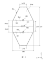
- Eighth Embodiment 12 is octagonal, and has holes H81, H82, and H83 formed therein.
- the shapes and sizes of the holes H81, H82, and H83 are similar to those of the holes H71 to H73 according to the seventh embodiment.
- the planar shape of the first excitation electrode 814a is an octagon obtained by removing a square from the first excitation electrode 714a according to the seventh embodiment into a triangular shape. That is, the first excitation electrode 814a has a side extending in the Z'-axis direction, a side extending in the X-axis direction, and a side connecting these sides.
- the dimension of the side of the first excitation electrode 814a extending in the X-axis direction is the short side length Le12
- the dimension of the side extending in the Z'-axis direction is the long side length Le11.
- the short side length Le12 is smaller than the second electrode length Le2, and the long side length Le11 is smaller than the first electrode length Le1.
- the short side length Le12 is smaller than the long side length Le11.
- the geometric centers of holes H81, H82, and H83 are aligned in the Z'-axis direction.
- the distance between the geometric center of hole H81 and the geometric center of hole H82 in the Z'-axis direction (hereinafter referred to as "hole spacing Ph12'") is smaller than the hole spacing Ph12 in the seventh embodiment (Ph12' ⁇ Ph12).
- hole spacing Ph13' The distance between the geometric center of hole H81 and the geometric center of hole H83 in the Z'-axis direction (hereinafter referred to as "hole spacing Ph13'”) is smaller than the hole spacing Ph13 in the seventh embodiment (Ph13' ⁇ Ph13).
- the sum of the hole spacing Ph12' and the hole spacing Ph13' is greater than the long side length Le11 (Le11 ⁇ Ph12' + Ph13').
- the hole spacing Ph12' and the hole spacing Ph13' are different from each other (Ph12' ⁇ Ph13').
- the magnitude relationship between the hole spacing Ph12', the hole spacing Ph13', and the long side length Le11 is not limited to Le11 ⁇ Ph12' + Ph13'.
- the relationship between the crystal thickness Tq and the first electrode length Le1 is 45 ⁇ Le1/Tq ⁇ 120.
- the relationship between the crystal thickness Tq and the second electrode length Le2 is 45 ⁇ Le2/Tq ⁇ 120.
- planar shape of the first excitation electrode is square as in this embodiment
- the planar shape of the first hole is not particularly limited, as in the case where the planar shape of the first excitation electrode is rectangular.
- the planar shape of the first hole formed in the square-shaped first excitation electrode may be a rectangle with long sides extending in the X-axis direction, a rectangle with long sides extending in the Z'-axis direction, a square, another polygonal shape, a circle, an ellipse, or a combination of these.
- the first hole formed in the square-shaped first excitation electrode may include a plurality of small holes.
- the square-shaped first excitation electrode may have a second hole formed in the center in the Z'-axis direction of the portion on the negative side of the Z'-axis direction with respect to the first hole, and a third hole formed in the center in the Z'-axis direction of the portion on the positive side of the Z'-axis direction with respect to the first hole. Also, the square-shaped first excitation electrode may have a fourth hole formed in the center in the X-axis direction of the portion on the negative side of the X-axis direction with respect to the first hole, and a fifth hole formed in the center in the X-axis direction of the portion on the positive side of the X-axis direction with respect to the first hole.
- Fig. 14 is a diagram showing a simulation result in the first example.
- the first example is a vibration simulation of a quartz crystal vibrating element including a first excitation electrode according to the first embodiment
- the comparative example is a vibration simulation of a quartz crystal vibrating element that is the same as the first example except that the first hole is not formed.
- the electromechanical coupling coefficient K of the main mode S0 is 6.87% in the comparative example, but is improved to 7.08 in the first example.
- the electromechanical coupling coefficient K of the inharmonic mode S1Z which has a frequency closest to the main mode S0, is 2.27% in the comparative example, but is reduced to 0.08 in the first example. Looking at the distribution of vibrations of the inharmonic mode S1Z, the vibration range in the center is wider in the first example, which causes the vibrations of opposite phases to cancel each other out, which is thought to have reduced the K of the inharmonic mode S1Z.
- the reduced K of the inharmonic mode S1Z reduces the influence of the inharmonic mode S1Z on the main mode S0, which is thought to have improved the K of the main mode S0.
- the electromechanical coupling coefficients K of the main mode S0 and the inharmonic mode S1Z are improved compared to the comparative example.
- Figures 15 and 16 plot the simulation results based on an example in which the shape of the first hole portion from the first example was changed to a rectangular shape based on the second embodiment, an example in which the shape of the first hole portion from the first example was changed to a circular shape based on the third embodiment, and an example in which the shape of the first hole portion from the first example was changed to a square shape based on the fourth embodiment.
- FIG. 17 is a graph showing the effect of the area ratio of the first hole portion in a square-shaped first excitation electrode.
- Figure 18 is a graph showing the effect of the area ratio of the first hole portion in a square-shaped first excitation electrode.
- Figure 19 is a graph showing the optimal condition for the area ratio of the first hole portion in a square-shaped first excitation electrode.
- the vertical axis of Fig. 17 indicates the electromechanical coupling coefficient K (%) of the main mode S0
- the vertical axis of Fig. 18 indicates the electromechanical coupling coefficient K (%) of the inharmonic mode S1Z.
- Figure 20 is a graph showing the conditions under which the K of the S0 mode is improved in a rectangular first excitation electrode.
- Figure 21 is a graph showing the conditions under which the K of the S0 mode is maximized in a rectangular first excitation electrode.
- Figure 22 is a graph showing the conditions under which the K of the S1Z mode is minimized in a rectangular first excitation electrode.
- the horizontal axis of Figures 20 to 22 is the ratio Le2/Le1 of the second electrode length Le2 to the first electrode length Le1 of the first excitation electrode.
- the conditional expression (3) for Har(SQ) is expressed by the following approximation, which has been described with reference to FIG. 19.
- the above condition range is also calculated by multiplying the conditional expression (1) related to Har(SQ) and the conditional expression (5) related to Har(N) in the same manner as the conditional range when 0.5 ⁇ Le2/Le1 ⁇ 1.3 and Le2/Le1 ⁇ 1.0.
- the above conditional expression is also calculated by multiplying the conditional expression (3) related to Har(SQ) and the conditional expression (6) related to Har(N) in the same manner as the conditional expression when 0.5 ⁇ Le2/Le1 ⁇ 1.3 and Le2/Le1 ⁇ 1.0.
- the conditional expression for minimizing the electromechanical coupling coefficient K of the inharmonic mode S1Z in the rectangular first excitation electrode was calculated by multiplying the conditional expression (7) for Har(SQ) and the conditional expression (8) for Har(N).
- the conditional expression (7) for Har(SQ) is expressed by the following approximation, which has been described with reference to FIG. 19.
- Har(SQ) 1.05 ⁇ (Le2/Tq) -0.92 ⁇ 0.01...(7)
- Fig. 23 is a diagram showing a simulation result in the second example.
- the second example is a vibration simulation of a quartz crystal vibrating element having a first excitation electrode according to the seventh embodiment
- the comparative example is a vibration simulation of a quartz crystal vibrating element that is the same as the second example except that the first hole, the second hole, and the third hole are not formed.
- the second example has the same conditions as the first example except for the second hole and the third hole.
- Second Example Quartz crystal piece Cut angle AT cut Planar shape: Square Top surface dimensions: 140 ⁇ m x 140 ⁇ m Thickness Tq: 1 ⁇ m Main mode S0: 1.45GHz
- First excitation electrode Material Aluminum (Al) or aluminum copper alloy (AlCu)
- Electrode thickness Te 0.05 ⁇ m First hole (hole H71)
- First hole length Lh11 5 ⁇ m 2nd hole length
- Lh12 15 ⁇ m
- Planar shape square Planar dimensions: 5 ⁇ m x 5 ⁇ m Hole spacing Ph12: 30 ⁇ m Hole spacing Ph13: 30 ⁇ m
- the electromechanical coupling coefficient K of the main mode S0 is 6.87(%) in the comparative example, but is improved to 7.38 in the second embodiment.
- the electromechanical coupling coefficient K of the inharmonic mode S1Z which has a frequency closest to the main mode S0, is 2.27(%) in the comparative example, but is reduced to 0.45 in the second embodiment.
- the electromechanical coupling coefficient K of the inharmonic mode S2Z which has a frequency next closest to the main mode S0 after the inharmonic mode S1Z, is 1.38(%) in the comparative example, but is reduced to 0.92 in the second embodiment.
- the electromechanical coupling coefficient K of the inharmonic mode S3Z which has the next closest frequency to the main mode S0 after the inharmonic mode S2Z, is 0.98(%) in the comparative example, but is reduced to 0.41 in the second example.
- the electromechanical coupling coefficient K of the main mode S0, the inharmonic mode S1Z, the inharmonic mode S2Z, and the inharmonic mode S1Z is improved compared to the comparative example.
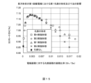
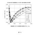
- FIG. 24 is a graph showing the influence of the dimensions of the first hole and the positions of the second and third holes.
- the horizontal axis of FIG. 24 represents the hole spacing Ph12, Ph13 ( ⁇ m), and the vertical axis of FIG. 24 represents the electromechanical coupling coefficient K (%) of the main mode S0.
- Figure 24 is a graph plotting the simulation results of the electromechanical coupling coefficient K of the main mode S0 corresponding to the hole spacing Ph12 and the hole spacing Ph13 when the first hole length Lh11 and the second hole length Lh12 of the hole H71 in the second embodiment are changed.
- the electromechanical coupling coefficient K of the main mode S0 changes in the same manner with respect to the changes in the hole interval Ph12 and the hole interval Ph13, even when the first hole length Lh11 and the second hole length Lh12 of the hole H71 are changed.
- the electromechanical coupling coefficient K of the main mode S0 decreases monotonically.
- the electromechanical coupling coefficient K of the main mode S0 increases monotonically.
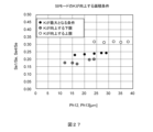
- Fig. 25 is a graph showing the influence of the shape of the first excitation electrode and the positions of the second and third holes.
- Fig. 26 is a graph showing the relationship between the short side length and the hole spacing.
- the horizontal axis of Fig. 25 shows the hole spacing Ph12, Ph13 ( ⁇ m), and the vertical axis of Fig. 25 shows the electromechanical coupling coefficient K (%) of the main mode S0.
- the horizontal axis of Fig. 26 shows the short side length Le12 ( ⁇ m), and the vertical axis of Fig. 26 shows the hole spacing Ph12, Ph13 ( ⁇ m).
- Conditions other than the planar shape of the first excitation electrode and the hole intervals Ph12, Ph13 are the same as those in the second embodiment.
- the shape of the graph of the electromechanical coupling coefficient K of the main mode S0 is similar to the graph shown in FIG. 24.
- the graph of the electromechanical coupling coefficient K of the main mode S0 slides in the horizontal direction according to the magnitude of the short side length Le12.
- the graph in FIG. 26 plots these results.
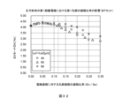
- Fig. 27 is a graph showing the area conditions under which K of the S0 mode is improved.
- Fig. 28 is a graph showing the area conditions under which K of the S0 mode is improved.
- the horizontal axis of Figs. 27 and 28 indicates the hole intervals Ph12, Ph13 ( ⁇ m).
- the vertical axis of Fig. 27 indicates the area ratio Se1/Se of the area Se1 of the portion on the negative side of the Z'-axis direction of the second hole portion in the first excitation electrode to the electrode area Se of the first excitation electrode.
- the vertical axis of Fig. 27 is also the area ratio Se4/Se of the area Se4 of the portion of the third hole portion in the first excitation electrode on the positive side of the Z'-axis direction to the electrode area Se of the first excitation electrode.
- hole intervals Ph12 and Ph13 at which the electromechanical coupling coefficient K of the main mode S0 is maximized are read from FIG. 25, and the area ratios Se1/Se and Se4/Se at these hole intervals Ph12 and Ph13 are calculated and plotted on the graph in FIG. 27.
- the upper and lower limits of the area ratios Se1/Se and Se4/Se at which the electromechanical coupling coefficient K of the main mode S0 is improved compared to the comparative example are substantially constant, regardless of the short side length Le12.
- the area ratios Se1/Se and Se4/Se at which the electromechanical coupling coefficient K of the main mode S0 is maximized are substantially constant, regardless of the short side length Le12.
- the electromechanical coupling coefficient K of the main mode S0 is improved compared to the comparative example.
- the electromechanical coupling coefficient K of the main mode S0 is maximized.
- the upper and lower limits of the area ratios Se1/Se2 and Se4/Se3 at which the electromechanical coupling coefficient K of the main mode S0 is improved compared to the comparative example are substantially constant, regardless of the short side length Le12.
- the area ratios Se1/Se2 and Se4/Se3 at which the electromechanical coupling coefficient K of the main mode S0 is maximized are substantially constant, regardless of the short side length Le12.
- the electromechanical coupling coefficient K of the main mode S0 is improved compared to the comparative example.
- the electromechanical coupling coefficient K of the main mode S0 is maximized.
- Fig. 29 is a graph showing the influence of the dimensions of the notched first hole in the rectangular first excitation electrode.
- Fig. 30 is a graph showing the influence of the dimensions of the notched first hole in the rectangular first excitation electrode.
- Fig. 31 is a graph showing the condition under which K in the S0 mode is maximized in the rectangular first excitation electrode.
- the horizontal axis of Figs. 29 and 30 shows the area ratio Sh/Se of the hole area Sh of the first hole to the electrode area Se of the first excitation electrode, the vertical axis of Fig.
- FIG. 29 shows the electromechanical coupling coefficient K (%) of the main mode S0
- the vertical axis of Fig. 30 shows the electromechanical coupling coefficient K (%) of the inharmonic mode S1Z.
- the horizontal axis of FIG. 31 indicates the ratio Wh11/Tq of the hole length Wh11 to the quartz crystal thickness Tq
- Quartz crystal piece Cut angle AT cut Planar shape: Square Top surface dimensions: 140 ⁇ m x 140 ⁇ m Thickness Tq: 1 ⁇ m
- First excitation electrode Material Aluminum (Al) or aluminum copper alloy (AlCu)
- the electromechanical coupling coefficient K of the main mode S0 shows an upwardly convex graph within the range of 0 ⁇ Har ⁇ 0.08.
- the electromechanical coupling coefficient K of the inharmonic mode S1Z shows a downward convex graph within the range of 0 ⁇ Har ⁇ 0.08.
- Figs. 32 and 33 are graphs showing the effect of the area ratio of the hole in the square-shaped first excitation electrode.
- the electromechanical coupling coefficient K of the main mode S0 shows an upwardly convex graph in the range of 0 ⁇ Har ⁇ 0.30.
- the electromechanical coupling coefficient K of the inharmonic mode S1Z is a downwardly convex graph in the range of 0 ⁇ Har ⁇ 0.20.
- the electromechanical coupling coefficient K of the inharmonic mode S1Z is further lower in the range of 0.025 ⁇ Har ⁇ 0.075.
- An excitation electrode provided on a main surface, When the dimension of the excitation electrode in the first direction is Le1 and the dimension of the piezoelectric piece in the third direction is Tq, 45 ⁇ Le1/Tq ⁇ 120 The relationship is established, A first hole portion is formed in a center portion of the excitation electrode in the first direction, the first hole portion penetrating the excitation electrode along the third direction. Piezoelectric vibration element.
- ⁇ 2> 60 ⁇ Le1/Tq The relationship between The piezoelectric vibration element according to ⁇ 1>.
- the first hole portion is formed in a central portion of the excitation electrode in the second direction and is spaced apart from an end portion of the excitation electrode extending in the first direction.
- the first hole portion opens in the second direction at an end portion of the excitation electrode extending in the first direction.
- the first hole portion has a plurality of small holes.
- the piezoelectric vibration element according to any one of ⁇ 1> to ⁇ 4>.
- ⁇ 6> When the dimension of the excitation electrode in the second direction is Le2, 10 ⁇ Le2/Tq ⁇ 45 The relationship is established as follows: ⁇ 5> A piezoelectric vibration element according to any one of ⁇ 1> to ⁇ 5>.
- ⁇ 7> When the dimension of the excitation electrode in the second direction is Le2, 45 ⁇ Le2/Tq ⁇ 120 The relationship is established, The first hole is formed in a center portion of the excitation electrode in the second direction.
- ⁇ 5> A piezoelectric vibration element according to any one of ⁇ 1> to ⁇ 5>.
- the piezoelectric strip is a quartz crystal strip.
- ⁇ 7> A piezoelectric vibration element according to any one of ⁇ 1> to ⁇ 7>.
- the crystal piece is AT cut.
- the second direction is a direction parallel to the X-axis of the crystal axis of the quartz crystal piece.
- the crystal piece is BT cut.
- the second direction is a direction parallel to the X-axis of the crystal axis of the quartz crystal piece.
- the first hole portion has a longitudinal direction along a direction perpendicular to a longitudinal direction of the excitation electrode.
- the piezoelectric vibration element according to any one of ⁇ 1> to ⁇ 9> and ⁇ 14> to ⁇ 21>.
- the first hole portion has a longitudinal direction parallel to a longitudinal direction of the excitation electrode.
- the piezoelectric vibration element according to any one of ⁇ 1> to ⁇ 9> and ⁇ 14> to ⁇ 21>.
- a second hole is further formed in a center portion in the first direction of a portion of the excitation electrode on a negative side in the first direction with respect to the first hole;
- a third hole portion is further formed in a center portion in the first direction of a portion of the excitation electrode on a positive side in the first direction with respect to the first hole portion;
- the second hole portion is formed at a position that divides an area of a portion of the excitation electrode on a negative side in the first direction with respect to the first hole portion in half in the first direction
- the third hole portion is formed at a position that divides an area of a portion of the excitation electrode on a positive side in the first direction with respect to the first hole portion in half in the first direction.
- the area of the second hole portion is smaller than the area of the first hole portion.
- the piezoelectric vibration element according to any one of ⁇ 26> to ⁇ 31>.
- the thickness-shear vibration mode is the dominant vibration mode.
- the piezoelectric vibration element according to any one of ⁇ 1> to ⁇ 32>.
- the main component of the excitation electrode is aluminum.
- ⁇ 35> The piezoelectric vibration element according to any one of ⁇ 1> to ⁇ 34>, A first cover member; a second cover member that is joined to the piezoelectric vibration element or the first cover member and forms a space between the second cover member and the first cover member to accommodate a vibration portion of the piezoelectric vibration element; Equipped with Piezoelectric vibrator.
- ⁇ 36> The piezoelectric vibrator according to ⁇ 35>, a mounting substrate on which the piezoelectric vibrator is mounted; a lid that is joined to the mounting substrate and forms a space between the mounting substrate and the lid to accommodate the piezoelectric vibrator; Piezoelectric oscillator.
- the embodiment of the present invention is not limited to quartz crystal resonators, but can also be applied to other piezoelectric resonators (Piezoelectric Resonator Units).
- piezoelectric pieces suitable for use in the piezoelectric resonator of this embodiment include piezoelectric ceramics such as lead zirconate titanate (PZT) and aluminum nitride, and piezoelectric single crystals such as lithium niobate and lithium tantalate, but the present invention is not limited to these and can be selected as appropriate.
- Embodiments of the present invention can be applied as appropriate to any device that performs electromechanical energy conversion using the piezoelectric effect, such as a timing device, sound generator, oscillator, or load sensor, without any particular limitations.
- a piezoelectric vibration element As described above, according to one aspect of the present invention, it is possible to provide a piezoelectric vibration element, a piezoelectric vibrator, and a piezoelectric oscillator that can improve the electromechanical coupling coefficient.
Landscapes
- Physics & Mathematics (AREA)
- Acoustics & Sound (AREA)
- Piezo-Electric Or Mechanical Vibrators, Or Delay Or Filter Circuits (AREA)
Abstract
圧電振動素子(10)は、第1方向及び第1方向と交差する第2方向に延在する主面を有し、第1方向及び第2方向と交差する第3方向に厚さを有する圧電片(11)と、主面(12a)に設けられた励振電極(14a)とを備え、励振電極(14a)の第1方向に沿った寸法を(Le1)、圧電片(11)の第3方向に沿った寸法を(Tq)としたとき、45≦Le1/Tq≦120の関係が成り立ち、励振電極(14a)の第1方向における中央部に、第3方向に沿って励振電極(14a)を貫通する第1孔部(H1)が形成されている。
Description
本発明は、圧電振動素子、圧電振動子及び圧電発振器に関する。
移動通信端末、通信基地局、家電などの各種電子機器において、タイミングデバイス、センサ又は発振器等の用途に圧電振動素子が用いられている。圧電振動素子は、一対の主面を有する圧電片と、圧電片の一対の主面に設けられた一対の励振電極を備える。
例えば、特許文献1には、水晶片の両主面に対向した励振電極を有する水晶振動子において、励振電極の中央領域に穴を設けて質量を減じ、基本波振動に対するオーバトーン振動の振動周波数を遠ざけたことを特徴とする水晶振動子が開示されている。
しかしながら、高周波化のために水晶片を薄肉化した場合、特許文献1に記載の水晶振動子では、メインモードの基本波振動に対してインハーモニックモードの振動周波数を充分に遠ざけることが難しく、例えばメインモードの周波数から±1%程度の範囲にインハーモニックモードの周波数が存在する場合がある。このため、オーバートーンモードの周波数をメインモードの周波数から遠ざけるだけでは、メインモードにおけるインハーモニックモードの影響を充分に抑制することができないという問題が生じていた。
本発明はこのような事情に鑑みてなされたものであり、本発明の目的は、電気機械結合係数の改善を図ることができる圧電振動素子、圧電振動子及び圧電発振器を提供することである。
本発明の一態様に係る圧電振動素子は、第1方向及び第1方向と交差する第2方向に延在する主面を有し、1方向及び第2方向と交差する第3方向に厚さを有する圧電片と、主面に設けられた励振電極とを備え、励振電極の第1方向に沿った寸法をLe1、圧電片の第3方向に沿った寸法をTqとしたとき、45≦Le1/Tq≦120の関係が成り立ち、励振電極の第1方向における中央部に、第3方向に沿って励振電極を貫通する第1孔部が形成されている。
本発明によれば、電気機械結合係数の改善を図ることができる圧電振動素子、圧電振動子及び圧電発振器を提供することができる。
以下に本発明の実施形態を説明する。以下の図面の記載において、同一又は類似の構成要素は同一又は類似の符号で表している。図面は例示であり、各部の寸法や形状は模式的なものであり、本発明の技術的範囲を当該実施形態に限定して解するべきではない。
各図面には、各図面の相互の関係を明確にし、各部材の位置関係を理解する助けとするために、便宜的にX軸、Y’軸及びZ’軸からなる直交座標系を付すことがある。X軸、Y’軸及びZ’軸は各図面において互いに対応している。X軸、Y’軸及びZ’軸は、それぞれ、後述する水晶片11の結晶軸(Crystallographic Axes)に対応している。X軸は水晶の電気軸(極性軸)、Y軸は水晶の機械軸、Z軸は水晶の光学軸に、それぞれ相当する。Y’軸及びZ’軸は、それぞれ、Y軸及びZ軸をX軸の周りにY軸からZ軸の方向に35度15分±1分30秒回転させた軸である。
以下の説明において、X軸に平行な方向を「X軸方向」、Y’軸に平行な方向を「Y’軸方向」、Z’軸に平行な方向を「Z’軸方向」という。また、X軸、Y’軸及びZ’軸の矢印の先端方向を「正」又は「+(プラス)」、矢印とは反対の方向を「負」又は「-(マイナス)」という。なお、便宜的に、+Y’軸方向を上方向、-Y’軸方向を下方向として説明するが、水晶振動素子10、水晶振動子1、及び水晶発振器100の上下の向きは限定されるものではない。また、X軸及びZ’軸によって特定される面をZ’X面とし、他の軸によって特定される面についても同様とする。
<第1実施形態>
まず、図1を参照しつつ、一実施形態に従う水晶発振器の概略構成について説明する。図1は、第1実施形態に係る水晶発振器の断面図である。
以下の説明において、圧電発振器として、水晶振動子(Quartz Crystal Resonator Unit)を備えた水晶発振器(XO:Crystal Oscillator)を例に挙げて説明する。また、圧電振動子(Piezoelectric Resonator Unit)として、水晶振動素子(Quartz Crystal Resonator)を備えた水晶振動子(Quartz Crystal Resonator Unit)を例に挙げて説明する。また、圧電振動素子として、水晶片(Quartz Crystal Element)を備えた水晶振動素子を例に挙げて説明する。水晶片は、印加電圧に応じて振動する圧電体(圧電片)の一種である。なお、圧電発振器は、水晶振動子に限定されるものではなく、セラミック等の他の圧電体を利用するものであってもよい。同様に、圧電振動子は、水晶振動子に限定されるものではなく、セラミック等の他の圧電体を利用するものであってもよい。また同様に、圧電振動素子は、水晶振動素子に限定されるものではなく、セラミック等の他の圧電体を利用するものであってもよい。
図1に示すように、水晶発振器100は、水晶振動子1と、実装基板130と、蓋体140と、電子部品156とを備える。
水晶振動子1及び電子部品156は、実装基板130と蓋体140との間に形成される空間に収容される。実装基板130及び蓋体140によって形成される空間は、例えば気密に封止される。なお、この空間は、真空状態で気密に封止されてもよく、不活性ガス等の気体が充填された状態で気密に封止されてもよい。
実装基板130は、平板状の回路基板である。実装基板130は、例えば、ガラスエポキシ板と、ガラスエポキシ板にパターニングされた配線層とを含んで構成される。
水晶振動子1は、実装基板130の一方の面(図1における上面)の上に設けられる。より詳細には、水晶振動子1は、ボンディングワイヤ166によって実装基板130の配線層に電気的に接続されている。また、半田153によって、水晶振動子1と実装基板130の配線層とが接合されている。これにより、水晶振動子1は、実装基板130と蓋体140との間に形成される空間に封止される。
蓋体140は、一方の側(図1における下側)が開口した、有底の開口部を含む。言い換えると、蓋体140は、平板状の天壁部と、天壁部の外縁から実装基板130に向かって延在する側壁部と、側壁部の先端から外側に延在するフランジ部とを含む。フランジ部は、実装基板130の一方の面(図1における上面)に接合される。これにより、蓋体140の内部に、実装基板130に接合された水晶振動子1が収容される。蓋体140は、金属材料によって構成されており、例えば金属板の絞り加工によって形成される。
電子部品156は、実装基板130の一方の面(図1における上面)の上に設けられる。より詳細には、半田153によって実装基板130の配線層と電子部品156とが接合されている。これにより、電子部品156は、実装基板130に実装される。
電子部品156は、実装基板130の配線層を通して、水晶振動子1に電気的に接続される。電子部品156は、例えばコンデンサやICチップ等を含んで構成される。電子部品156は、例えば、水晶振動子1を発振させる発振回路の一部、又は、水晶振動子1の温度特性を補償する温度補償回路の一部等である。電子部品156が温度補償回路を含む場合、水晶発振器100は、温度補償水晶発振器(TCXO:Temperature Compensated Crystal Oscillator)と呼ばれることがある。
次に、図2から図5を参照しつつ、一実施形態に従う水晶振動子の概略構成について説明する。図2は、第1実施形態に係る水晶振動子の断面図である。図3は、第1実施形態に係る水晶振動素子の平面図である。図4は、第1実施形態に係る第1励振電極の平面図である。図5は、第1実施形態に係る振動部の断面図である。なお、図2は、図3に示したII-II線に沿ったY’Z’面に平行な断面を示している。図5は、図3に示したV-V線に沿ったY’Z’面に平行な断面を示している。
Z’軸方向は「第1方向」の一例に相当し、X軸方向は「第2方向」の一例に相当し、Y’軸方向は「第3方向」の一例に相当する。但し、第1方向、第2方向及び第3方向は上記に限定されるものではない。例えば、X軸方向が第1方向であり、Z’軸方向が第2方向であってもよい。
水晶振動子1は、水晶振動素子10と、上蓋20と、接合部30と、絶縁層40と、支持基板50と、を備える。絶縁層40及び支持基板50は「第1蓋部材」の一例に相当し、上蓋20は、「第2蓋部材」の一例に相当する。
水晶振動素子10は、圧電効果により電気エネルギーと機械エネルギーとを相互に変換する電気機械エネルギー変換素子である。水晶振動素子10のメインモードの周波数は、例えばGHz帯であり、例えば1.0GHz~2.0GHz程度であり、例えば1.45GHz程度である。水晶振動素子10のインハーモニックモードの周波数は、例えば、メインモードの周波数の1%程度の範囲内に存在する。水晶振動素子10は、薄片状の水晶片(Quartz Crystal Element)11と、一対の励振電極を構成する第1励振電極14a及び第2励振電極14bと、一対の引出電極を構成する第1引出電極15a及び第2引出電極15bと、一対の接続電極を構成する第1接続電極16a及び第2接続電極16bと、ビア電極17とを備えている。
水晶片11は、互いに対向する上面12a及び下面12bを有している。上面12aは、上蓋20に対向する側に位置している。下面12bは、支持基板50に対向する側に位置している。上面12a及び下面12bは、水晶片11の一対の主面に相当する。
水晶片11は、例えば、ATカット型の水晶結晶である。ATカット型の水晶結晶は、XZ’面が主面となり、Y’軸と平行な方向が厚みとなるように形成される。一例として、上面12aを平面視したとき(以下、単に「平面視」とする。)、水晶片11の形状(以下、「平面形状」とする。)は、Z’軸方向に延在する長辺と、X軸方向に延在する短辺とを有する長方形状である。また、水晶片11は、Y’軸方向に厚さを有する。一例として、水晶片11は、厚さが一様な平板状をなしている。
なお、水晶片の平面形状は上記に限定されるものではなく、短辺がZ’軸方向に延在し、長辺がX軸方向に延在する長方形状であってもよい。水晶片の平面形状は、多角形状、円形状、楕円形状、又はこれらの組合せであってもよい。また、水晶片は平板状に限定されるものではなく、水晶片は、第1励振電極14a及び第2励振電極14bに重なる部分の厚さが周囲の厚さよりも大きい、いわゆるメサ型構造であってもよい。水晶片は、第1励振電極14a及び第2励振電極14bに重なる部分の厚さが周囲の厚さよりも小さい、いわゆる逆メサ型構造であってもよい。水晶片の厚さを部分的に変化させる場合、厚さの変化量が連続的に変化するコンベックス構造であってもよく、厚さの変化量が不連続に変化するベベル構造であってもよい。
ATカット型の水晶片11は、人工水晶(Synthetic Quartz Crystal)の結晶軸であるX軸、Y軸、Z軸のうち、Y軸及びZ軸をX軸の周りにY軸からZ軸の方向に35度15分±1分30秒回転させた軸をそれぞれY’軸及びZ’軸とし、XZ’面を主面として切り出されたものである。
ATカット型の水晶片11を用いた水晶振動素子10は、広い温度範囲で高い周波数安定性を有する。また、ATカット水晶振動素子は、経時変化特性にも優れている上、低コストで製造することが可能である。さらに、ATカット水晶振動素子は、厚みすべり振動モード(Thickness Shear Vibration Mode)を主要振動として用いる。
なお、水晶片のカット角は上記に限定されるものではない。ATカット型の水晶片11におけるY’軸及びZ’軸の回転角は、35度15分から-5度以上+15度以下の範囲で傾いてもよい。また、水晶片のカット角は、ATカット以外の異なるカット、例えばBTカット、GTカット、SCカット等を適用してもよい。
水晶片11は、振動部11Aと、開口部11Bと、保持部11Cと、を含む。
水晶片11の振動部11Aは、前述したように、厚みすべり振動モードを主要振動として所定の共振周波数で振動する。水晶片11の開口部11Bは、上面12aを平面視したときに、振動部11Aの周りを囲むように形成された開口である。開口部11Bは、Z’軸方向に平行な水晶片11の厚さ方向に貫通し、後述する空洞部41に通じている。開口部11Bは、振動部11Aと保持部11Cとの間が、例えば10μm程度離間するように、形成される。水晶片11の保持部11Cは、振動部11Aの端部(図2において下端部)を保持する。保持部11Cは、例えば、振動部11AにおけるX軸負方向側の辺に接続している。
第1励振電極14a及び第2励振電極14bは、振動部11Aに交番電圧を印加して、振動部11Aを励振する。第1励振電極14a及び第2励振電極14bは、振動部11Aの中央部に設けられている。第1励振電極14aは、上面12aに設けられ、第2励振電極14bは、下面12bに設けられている。第1励振電極14aと第2励振電極14bとは、振動部11Aを挟んでY’軸方向において互いに対向している。
第1励振電極14aの平面形状は、Z’軸方向に延在する長辺と、X軸方向に延在する短辺とを有する長方形状である。また、第1励振電極14aはY’軸方向に厚さを有する。第2励振電極14bも同様の形状である。
なお、第1励振電極及び第2励振電極の平面形状は上記に限定されるものではない。第1励振電極及び第2励振電極の平面形状は、X軸方に延在する長辺を有する長方形状であってもよい。また、第1励振電極及び第2励振電極の平面形状は、正方形状、多角形状、円形状、楕円形状又はこれらの組み合わせであってもよい。
図4及び図5に示すように、平面視における第1励振電極14aの中央部には、Y’軸方向に沿って第1励振電極14aを貫通する孔部H1が形成されている。孔部H1は、「第1孔部」の一例に相当する。平面視において、孔部H1の中央部は、Z’軸方向における第1励振電極14aの中央部に位置し、X軸方向における第1励振電極14aの中央部に位置している。言い換えると、孔部H1は、その幾何中心が第1励振電極14aの幾何中心に一致するよう形成されている。孔部H1は、第1励振電極14aの長辺及び短辺に沿った端部から離間している。孔部H1の平面形状は、Z’軸方向に延在する短辺と、X軸方向に延在する長辺とを有する長方形状である。すなわち、孔部H1の長手方向は、第1励振電極14aの長手方向と直交する方向である。
なお、孔部は、Z’軸方向における第1励振電極14aの中央部に位置していれば、X軸方向における第1励振電極14aの中央部から離間してもよい。
なお、孔部の平面形状は上記に限定されるものではない。孔部の平面形状は、多角形状、円形状、楕円形状又はこれらの組み合わせであってもよい。また、孔部H1は、複数の小孔を含んでもよく、複数の小孔の形状は特に限定されるものではない。
第2励振電極14bには孔部は形成されておらず、孔部H1は、Y’軸方向において第2励振電極14bと対向している。第1励振電極14aと第2励振電極14bとがY’軸方向において重なる振動領域Rvでは水晶片11が励振され、孔部H1とY’軸方向において重なる非振動領域Rnvにおいては水晶片11が励振されない。
なお、第2励振電極の中央部にも、第1励振電極と同様に孔部が形成されてもよい。この場合、第2励振電極に形成された孔部の平面形状及び面積は、第1励振電極に形成された孔部の平面形状及び面積と略同一であることが望ましい。また、第2励振電極に形成された孔部の端部と、第1励振電極に形成された孔部の端部とは、Y’軸方向において重なることが望ましい。水晶片11に印加される電圧の向きや大きさの乱れに起因したスプリアス振動の発生を抑制するためである。
図4及び図5に示すように、水晶片11のY’軸方向に沿った寸法を水晶厚Tqとする。第1励振電極14aのZ’軸方向に沿った寸法を第1電極長Le1とし、第1励振電極14aのX軸方向に沿った寸法を第2電極長Le2とし、第1励振電極14aのY’軸方向に沿った寸法を電極厚Teとする。孔部H1のZ’軸方向に沿った寸法を第1孔部長Lh11とし、孔部H1のX軸方向に沿った寸法を第2孔部長Lh12とする。孔部H1の幾何学的な中心の、第1励振電極14aの短辺からのZ’軸方向に沿った距離を第1孔部距離Ph1とする。孔部H1の幾何学的な中心の、第1励振電極14aの長辺からのX軸方向に沿った距離を第2孔部距離Ph2とする。
水晶厚Tqは、例えば0.5μm以上3μm以下の範囲内、例えば1μm程度である。第1電極長Le1は例えば120μm程度であり、第2電極長Le2は例えば50μm程度、電極厚は例えば0.05μm程度である。
水晶厚Tqと第1電極長Le1との間には、45≦Le1/Tq≦120の関係が成り立つ。45≦Le1/Tqの関係が成り立つことで、等価直列抵抗が小さくなるので発振条件を満たし易く、等価直列容量が大きくなるので寄生容量の影響を受け難い。60≦Le1/Tq≦120の関係が成り立つことが、さらに望ましい。Le1/Tq≦120の関係が成り立つことで、Z’軸方向に振動の腹が並ぶインハーモニックモード(以下、「第1方向インハーモニックモード」とする。)の周波数がメインモードの周波数に対して過度に接近することを抑制できる。
水晶厚Tqと第2電極長Le2との間には、10≦Le2/Tq≦45の関係が成り立つ。10≦Le2/Tqが成り立つことで、等価直列抵抗が小さくなるので発振条件を満たし易く、等価直列容量が大きくなるので寄生容量の影響を受け難い。Le2/Tq≦45が成り立つことで、X軸方向に振動の腹が並ぶインハーモニックモード(以下、「第2方向インハーモニックモード」とする。)の周波数がメインモードの周波数から充分に離れるため、第2方向インハーモニックモードを抑制しなくても、第2方向インハーモニックモードのメインモードに対する影響を低減することができる。
第1孔部長Lh11は、例えば5μm程度であり、第2孔部長Lh12は、例えば15μm程度である。第1孔部距離Ph1は、例えば第1電極長Le1の半分±10%程度である。すなわち、0.9×{(1/2)×Le1}≦Ph1≦1.1×{(1/2)×Le1}の関係が成り立つ。第2孔部距離Ph2は、例えば第2電極長Le2の半分±10%程度である。すなわち、0.9×{(1/2)×Le2}≦Ph2≦1.1×{(1/2)×Le2}の関係が成り立つ。
但し、第1電極長Le1、第2電極長Le2、第1孔部距離Ph1及び第2孔部距離Ph2の関係は上記に限定されるものではない。例えば、45≦Le1/Tq≦120、且つ、10≦Le2/Tq≦45の関係が成り立つ場合、0.9×{(1/2)×Le1}≦Ph1≦1.1×{(1/2)×Le1}の関係が成り立つのであれば、0.9×{(1/2)×Le2}≦Ph2≦1.1×{(1/2)×Le2}の関係が必ずしも成り立たなくてもよい。つまり、このような場合には、Ph2<0.9×{(1/2)×Le2}、又は、1.1×{(1/2)×Le2}<Ph2の関係が成り立ってもよい。
一方で、10≦Le1/Tq≦45、且つ、45≦Le2/Tq≦120の関係が成り立つ場合、0.9×{(1/2)×Le2}≦Ph2≦1.1×{(1/2)×Le2}の関係が成り立つのであれば、Ph1<0.9×{(1/2)×Le1}、又は、1.1×{(1/2)×Le1}<Ph1の関係が成り立ってもよい。
45≦Le1/Tq≦120、且つ、45≦Le2/Tq≦120の関係が成り立つ場合、0.9×{(1/2)×Le1}≦Ph1≦1.1×{(1/2)×Le1}の関係、及び、0.9×{(1/2)×Le2}≦Ph2≦1.1×{(1/2)×Le2}の関係、のうち少なくとも一方の関係が成り立てばよく、望ましくはその両方の関係が成り立つ。
第1引出電極15aは第1励振電極14aと第1接続電極16aとを電気的に接続し、第2引出電極15bは第2励振電極14bと第2接続電極16bとを電気的に接続する。第1引出電極15a及び第2引出電極15bは、振動部11Aから保持部11Cに亘って設けられている。第1引出電極15aは水晶片11の上面12aに設けられ、第2引出電極15bは水晶片11の下面12bに設けられている。第1引出電極15aは、振動部11Aにおいて第1励振電極14aに電気的に接続され、保持部11Cにおいて第1接続電極16aに電気的に接続されている。第2引出電極15bは、振動部11Aにおいて第2励振電極14bに電気的に接続され、保持部11Cにおいて第2接続電極16bに電気的に接続されている。
第1接続電極16a及び第2接続電極16bは、上蓋20に設けられた外部電極に電気的に接続するための端子である。第1接続電極16a及び第2接続電極16bは、保持部11Cに設けられている。また、第1接続電極16a及び第2接続電極16bは、水晶片11の上面12aに設けられている。
第1励振電極14a、第2励振電極14b、第1引出電極15a、第2引出電極15b、第1接続電極16a及び第2接続電極16bの材料は、例えば、アルミニウム(Al)、モリブデン(Mo)、金(Au)又は、アルミニウムを主成分とするアルミ銅合金(AlCu)である。これらの電極は、単層膜であってもよく、多層膜であってもよい。多層膜である場合、第1励振電極14a及び第2励振電極14bは、例えば、水晶との密着性が良好な下地層と、化学的安定性が良好な表面性とを含んでもよい。下地層は例えばクロム(Cr)層又はチタン(Ti)層であり、表面層は例えば金(Au)層である。
ビア電極17は、第2引出電極15bと第2接続電極16bとを電気的に接続する。ビア電極17は、水晶片11の上面12aから下面12bまで貫通して設けられている。ビア電極17の材料は、例えばアルミニウム(Al)であり、ビア電極17の厚さは、例えば1.0μmである。なお、ビア電極17の材料は、例えば銅(Cu)又はアルミニウムを主成分とするアルミ銅合金(AlCu)であってもよい。ビア電極17の厚さは、例えば0.5μm以上3.0μm以下の範囲内である。
上蓋20は、平坦な板状の部材である。平面視における上蓋20の寸法は、水晶振動素子10(水晶片11)の寸法と同一又は略同一である。上蓋20の厚さは、例えば100μm以上200μm以下の範囲内である。
上蓋20の材料は、例えば水晶である。これにより、接合部30及び水晶振動素子10との間の熱膨張係数差に起因する応力を低減することが可能となる。
なお、上蓋20は、水晶板である場合に限定されず、例えばセラミック板やガラス板などであってもよい。耐熱性のセラミック板によって上蓋を設ける場合、熱履歴に起因した水晶振動素子10の変形や熱応力の発生を抑制することができる。また、透明なガラス板によって上蓋を設ける場合、水晶振動素子10を封止した後で、外部から第1励振電極14aにレーザを照射して、共振周波数を調整することができる。
また、上蓋20は、導電性を有していてもよい。上蓋20が導電材料で構成されることによって、内部空間への電磁波の出入りを低減する電磁シールド機能が上蓋20に付与される。この場合、上蓋20は、鉄(Fe)及びニッケル(Ni)を含む合金である42アロイ、又は、鉄(Fe)、ニッケル(Ni)、コバルト(Co)を含むFe-Ni-Co系合金であるコバール等によって設けられるのが望ましい。Fe-Ni-Co系合金は常温付近での熱膨張率がガラスやセラミックと広い温度範囲で一致するため、熱応力の発生を抑制することができる。
接合部30は、水晶振動素子10と上蓋20とを接合する。接合された上蓋20と水晶振動素子10とによって、空間が形成される。空間は、振動部11Aの振動空間の一部を形成する。接合部30は、上蓋20及び水晶振動素子10のそれぞれの全周に亘って設けられている。具体的には、接合部30は、上蓋20の下面と水晶片11の上面12aとの間に設けられている。平面視において、接合部30は、枠形状に設けられている。接合部30の幅、つまり、外周と内周との差は、例えば約20μmである。
接合部30は、例えば、鉛ホウ酸系、錫リン酸系等の低融点ガラスによって設けられている。接合部30は、例えば、エポキシ系、ビニル系、アクリル系、ウレタン系又はシリコーン系の樹脂を含む有機系接着剤、水ガラスなどを含むケイ素系接着剤、セメントなどを含むカルシウム系接着剤、又は金錫(Au-Sn)系の共晶合金などの金属接合によって設けられてもよい。水晶振動素子10と上蓋20とは、シーム溶接によって接合されてもよい。
絶縁層40は、水晶振動素子10の振動部11Aに対応する部分に形成された空洞部41を含む。空洞部41は、凹形状を有しており、水晶片11の下面12bに設けられた第2励振電極14bとの間に空間を形成する。
絶縁層40は、水晶振動素子10と支持基板50とを接合する。より詳細には、絶縁層40は、水晶振動素子10の下面に形成され、支持基板50の上面と水晶片11の下面12bとを接合する。
絶縁層40の材料は、例えば二酸化ケイ素(SiO2)などを含むシリコン酸化膜である。これにより、水晶振動素子10との間の熱膨張係数差に起因する応力、及び、支持基板50との間の熱膨張係数差に起因する応力を低減することが可能となる。
絶縁層40の厚さは、0.5μm以上であることが望ましく、例えば1μm以上1.5μm以下の範囲内である。この場合、空洞部41のY’軸方向の深さは、例えば0.2μm以上0.5μm以下の範囲内である。
なお、絶縁層40の材料は、シリコン酸化膜に限定されるものではなく、シリコン窒化膜又はシリコン酸窒化膜、若しくは各種の接着剤であってもよい。
支持基板50は、水晶振動素子10及び絶縁層40を支持するように構成されている。具体的には、絶縁層40を介して、水晶片11の保持部11Cを支持している。
支持基板50は、例えば平坦な板状の基板である。平面視における支持基板50の寸法は、水晶振動素子10(水晶片11)の寸法と同一又は略同一である。支持基板50のY’軸方向に沿った厚さは、例えば50μm以上500μm以下の範囲内である。
支持基板50の材料は、例えば水晶である。これにより、水晶振動素子10及び絶縁層40との間の熱膨張係数差に起因する応力を低減することが可能となる。
なお、支持基板50は、水晶板である場合に限定されず、例えばセラミック板、シリコン基板又はガラス板などであってもよい。耐熱性のセラミック板によって支持基板50を設ける場合、熱履歴に起因した水晶振動素子10の変形を抑制することができる。
以上のように、第1励振電極14aの第1方向に沿った寸法をLe1、水晶片11の厚さをTqとし、45≦Le1/Tq≦120の関係が成り立つときに、第1励振電極14aの第1方向における中央部に貫通孔が形成される。これによれば、後述するように、第1方向に振動の腹が並ぶインハーモニックモードの電気機械結合係数を低下させることができ、メインモードの電気機械結合係数が上昇する。
次に、図6~図13を参照しつつ、第2~第9実施形態に係る第1励振電極214a~914aの構成について説明する。図6~図13は、第2~第9実施形態に係る第1励振電極214a~914aの平面図である。なお、下記の実施形態では、上記の第1実施形態と共通の事柄については記述を省略し、異なる点についてのみ説明する。特に、同様の構成による同様の作用効果については逐次言及しない。
<第2実施形態>
図6に示した第1励振電極214aに形成された孔部H2の平面形状は、Z’軸方向に延在する長辺と、X軸方向に延在する短辺とを有する長方形状である。すなわち、孔部H2の長手方向は、第1励振電極214aの長手方向と平行な方向である。
図6に示した第1励振電極214aに形成された孔部H2の平面形状は、Z’軸方向に延在する長辺と、X軸方向に延在する短辺とを有する長方形状である。すなわち、孔部H2の長手方向は、第1励振電極214aの長手方向と平行な方向である。
<第3実施形態>
図7に示した第1励振電極314aに形成された孔部H3の平面形状は、円形状である。
図7に示した第1励振電極314aに形成された孔部H3の平面形状は、円形状である。
<第4実施形態>
図8に示した第1励振電極414aに形成された孔部H4の平面形状は、Z’軸方向に延在する辺と、X軸方向に延在する辺とを有する正方形状である。
図8に示した第1励振電極414aに形成された孔部H4の平面形状は、Z’軸方向に延在する辺と、X軸方向に延在する辺とを有する正方形状である。
<第5実施形態>
図9に示した第1励振電極514aに形成された孔部H5は、複数の小孔H51を含んでいる。複数の小孔H51の平面形状は、例えば半径1μm程度の円形状である。複数の小孔H51は、Z’軸方向及びX軸方向に格子状に並んでいる。隣接する小孔H51の中心間の距離は、例えば3μm程度である。複数の小孔H51の数は、例えば21個である。
図9に示した第1励振電極514aに形成された孔部H5は、複数の小孔H51を含んでいる。複数の小孔H51の平面形状は、例えば半径1μm程度の円形状である。複数の小孔H51は、Z’軸方向及びX軸方向に格子状に並んでいる。隣接する小孔H51の中心間の距離は、例えば3μm程度である。複数の小孔H51の数は、例えば21個である。
なお、複数の小孔の平面形状、面積及び配置は、上記に限定されるものではない。複数の小孔の平面形状は、例えば、長方形状、正方形状、その他の多角形状、円形状、楕円形状又はこれらの組み合わせであってもよい。複数の小孔は、平面形状が互いに異なる異種の小孔を含んでもよい。複数の小孔は、面積が互いに異なる異種の小孔を含んでもよい。複数の小孔の配置は、例えば千鳥状又は同心円状であってもよい。
<第6実施形態>
図10に示した第1励振電極614aに形成された孔部H6は、第1励振電極614aの長辺に沿った端部においてX軸方向に開口する、切り欠き状の開口部である。孔部H6は、第1励振電極614aのX軸方向負方向側の端部に形成された切り欠き部H61と、第1励振電極614aのX軸方向正方向側の端部に形成された切り欠き部H62とを含んでいる。
図10に示した第1励振電極614aに形成された孔部H6は、第1励振電極614aの長辺に沿った端部においてX軸方向に開口する、切り欠き状の開口部である。孔部H6は、第1励振電極614aのX軸方向負方向側の端部に形成された切り欠き部H61と、第1励振電極614aのX軸方向正方向側の端部に形成された切り欠き部H62とを含んでいる。
切り欠き部H61と切り欠き部H62とは、互いに離間し、X軸方向において並んでいる。切り欠き部H61,H62の幾何中心は、第1励振電極614aの幾何中心を通りX軸方向に延在する中心線上に位置する。切り欠き部H61、H62の平面形状は、Z’軸方向に延在する短辺と、X軸方向に延在する長辺とを有する長方形状である。切り欠き部H61のZ’軸方向に沿った寸法を孔部長Wh11、切り欠き部H61のX軸方向に沿った寸法を孔部長Wh12、切り欠き部H62のZ’軸方向に沿った寸法を孔部長Wh21、切り欠き部H62のX軸方向に沿った寸法を孔部長Wh22とする。切り欠き部H61,H62はX軸方向を長手方向とする長方形状であるため、孔部長Wh11は孔部長Wh12よりも小さく(Wh11<Wh12)、孔部長Wh21は孔部長Wh22よりも小さい(Wh21<Wh22)。また、切り欠き部H61,H62は互いに離間しているため、孔部長Wh12と孔部長Wh22の和は、第2電極長Le2よりも小さい(Wh12+Wh22<Le2)。一例として、孔部長Wh11は孔部長Wh21と略等しく(Wh11=Wh21)、孔部長Wh12は孔部長Wh22と略等しい(Wh12=Wh22)。すなわち、切り欠き部H61の面積は、切り欠き部H62の面積と略等しい。
なお、2つの切り欠き部の位置、平面形状及び面積は、上記に限定されるものではない。2つの切り欠き部の幾何中心は、第1励振電極のX軸方向に延在する中心線から離間していてもよい。例えば、2つの切り欠き部は、Z’軸方向において間隔を空けて並んでもよい。このとき、孔部長Wh12と孔部長Wh22との和は、第2電極長Le2と同等以上となる(Le2≦Wh12+Wh22)。2つの切り欠き部の平面形状は、例えば、長方形状、正方形状、その他の多角形状、円形状、楕円形状又はこれらの組み合わせであってもよい。2つの切り欠き部の平面形状は、互いに異なってもよい。また、2つの切り欠き部の面積は、互いに異なってもよい。例えば、Wh11<Wh21又はWh11>Wh21の関係が成り立ってもよく、Wh12<Wh22又はWh12>Wh22の関係が成り立ってもよい。
なお、第1励振電極には、2つの切り欠き部の他に、追加の孔部がさらに形成されてもよい。追加の孔部は、例えば、2つの切り欠き部の間に、2つの切り欠き部から離間して形成される。追加の孔部の平面形状は特に限定されるものではなく、例えば、長方形状、正方形状、その他の多角形状、円形状、楕円形状又はこれらの組み合わせであってもよい。また、追加の孔部の面積は特に限定されるものではなく、2つの切り欠き部の面積よりも小さくても大きくてもよく、同等であってもよい。
<第7実施形態>
図11に示した第1励振電極714aには、孔部H71,H72,H73が形成されている。孔部H71,H72,H73のうち、孔部H71は第1実施形態の孔部H1と同様である。孔部H72は、「第2孔部」の一例に相当する。孔部H73は、「第3孔部」の一例に相当する。
図11に示した第1励振電極714aには、孔部H71,H72,H73が形成されている。孔部H71,H72,H73のうち、孔部H71は第1実施形態の孔部H1と同様である。孔部H72は、「第2孔部」の一例に相当する。孔部H73は、「第3孔部」の一例に相当する。
孔部H72は、第1励振電極714aのうち孔部H71に対してZ’軸方向負方向側の部分の、Z’軸方向における中央部に形成されている。また、孔部H72は、第1励振電極714aのX軸方向における中央部に形成されている。孔部H72は、孔部H71、第1励振電極714aのZ’軸方向負方向側の短辺、第1励振電極714aのX軸方向負方向側の長辺、及び第1励振電極714aのX軸方向正方向側の長辺から離間している。孔部H72は、孔部H71と、第1励振電極714aのZ’軸方向負方向側の短辺と、の間に設けられている。
孔部H73は、第1励振電極714aのうち孔部H71に対してZ’軸方向正方向側の部分の、Z’軸方向における中央部に形成されている。また、孔部H73は、第1励振電極714aのX軸方向における中央部に形成されている。孔部H73は、孔部H71、第1励振電極714aのZ’軸方向正方向側の短辺、第1励振電極714aのX軸方向負方向側の長辺、及び第1励振電極714aのX軸方向正方向側の長辺から離間している。孔部H73は、孔部H71と、第1励振電極714aのZ’軸方向正方向側の短辺と、の間に設けられている。
孔部H72,H73の平面形状は、Z’軸方向に延在する辺と、X軸方向に延在する辺とを有する正方形状である。孔部H72,73の各辺は、孔部H71の短辺と略同じ大きさである。したがって、孔部H72,H73のそれぞれの面積は、孔部H71の面積よりも小さい。
平面視したとき、孔部H71,H72,H73の幾何中心は、第1励振電極714aの幾何中心を通りZ’軸方向に延在する中心線上に位置し、Z’軸方向に並んでいる。すなわち、孔部H71,H72,H73の幾何学的な中心の、第1励振電極714aの長辺からのX軸方向に沿った距離は、いずれも第2孔部距離Ph2である。Z’軸方向における、孔部H71の幾何中心と孔部H72の幾何中心との間の距離(以下、「孔部間隔Ph12」とする。)は、第1電極長Le1の略4分の1であり、第1孔部距離Ph1の略2分の1である(Ph12=(1/4)×Le1,Ph12=(1/2)×Ph1)。Z’軸方向における、孔部H71の幾何中心と孔部H73の幾何中心との間の距離(以下、「孔部間隔Ph13」とする。)も同様である(Ph13=(1/4)×Le1,Ph13=(1/2)×Ph1)。したがって、孔部間隔Ph12と孔部間隔Ph13とは略等しい(Ph12=Ph13)。
第1励振電極714aの電極面積をSe、第1励振電極714aにおける孔部H72のZ’軸方向負方向側の部分の面積をSe1、第1励振電極714aにおける孔部H72のZ’軸方向正方向側であって孔部H71のZ’軸方向負方向側の部分の面積をSe2、第1励振電極714aにおける孔部H71のZ’軸方向正方向側であって孔部H73のZ’軸方向負方向側の部分の面積をSe3、第1励振電極714aにおける孔部H73のZ’軸方向正方向側の部分の面積をSe4とする。例えば、面積Se1~Se4は互いに略等しい(Se1≒Se2≒Se3≒Se4)。つまり、孔部H71が第1励振電極714aの面積をZ’軸方向において二等分する位置に形成されている。また、孔部H72は、第1励振電極714aのうち孔部H71のZ’軸方向負方向側の部分の面積を、Z’軸方向において二等分する位置に形成されている。また、孔部H73は、第1励振電極714aのうち孔部H71のZ’軸方向正方向側の部分の面積を、Z’軸方向において二等分する位置に形成されている。まとめると、孔部H71,H72,H73は、第1励振電極714aの電極面積SeをZ’軸方向において4等分する位置に形成されている。
なお、第2孔部は、第1励振電極のうち第1孔部に対してZ’軸方向負方向側の部分の、Z’軸方向における中央部に形成されるのであれば、その位置、平面形状及び大きさは、上記に限定されるものではない。同様に、第3孔部は、第1励振電極のうち第1孔部に対してZ’軸方向正方向側の部分の、Z’軸方向における中央部に形成されるのであれば、その位置、平面形状及び大きさは、上記に限定されるものではない。例えば、第2孔部及び第3孔部の幾何中心は、第1励振電極のZ’軸方向に延在する中心線から離間していてもよい。また、第2孔部及び第3孔部の幾何中心は、第1孔部の幾何中心とZ’軸方向において並んでいなくてもよい。第2孔部は、Ph12>(1/2)×Ph1又はPh12<(1/2)×Ph1の関係が成り立つ位置に形成されてもよく、第3孔部は、Ph13>(1/2)×Ph1又はPh13<(1/2)×Ph1の関係が成り立つ位置に形成されてもよい。また、第2孔部は、Se1>Se2又はSe1<Se2の関係が成り立つ位置に形成されてもよく、第3孔部は、Se3>Se4又はSe3<Se4の関係が成り立つ位置に形成されてもよい。
第2孔部及び第3孔部の平面形状は、X軸方向に延在する長辺を有する長方形状、Z’軸方向に延在する長辺を有する長方形状、その他の多角形状、円形状、楕円形状又はこれらの組み合わせであってもよい。また、第2孔部及び第3孔部は、複数の小孔を含んでもよく、第1励振電極のX軸方向正方向側又は負方向側に開口する切り欠き状の開口部を含んでもよい。第2孔部及び第3孔部のそれぞれの面積は、第1孔部の面積と略等しくてもよく、第1孔部の面積よりも大きくてもよい。第2孔部の面積と第3孔部の面積とは互いに異なってもよい。
<第8実施形態>
図12に示した第1励振電極814aは八角形状であり、第1励振電極814aには孔部H81,H82,H83が形成されている。孔部H81,H82,H83の形状及び大きさは、第7実施形態に係る孔部H71~73と同様である。
図12に示した第1励振電極814aは八角形状であり、第1励振電極814aには孔部H81,H82,H83が形成されている。孔部H81,H82,H83の形状及び大きさは、第7実施形態に係る孔部H71~73と同様である。
第1励振電極814aの平面形状は、第7実施形態に係る第1励振電極714aから四角を三角形状に削った八角形状である。すなわち、第1励振電極814aは、Z’軸方向に延在する辺と、X軸方向に延在する辺と、これらの辺を繋ぐ辺とを有している。第1励振電極814aのX軸方向に延在する辺の寸法を短辺長Le12とし、Z’軸方向に延在する辺の寸法を長辺長Le11とする。短辺長Le12は第2電極長Le2よりも小さく、長辺長Le11は第1電極長Le1よりも小さい。例えば、短辺長Le12は、長辺長Le11よりも小さい。
孔部H81は、その幾何中心が第1励振電極814aの幾何中心に一致するように形成されており、孔部H82,H83は、Se1=Se2=Se3=Se4=(1/4)×Seとなる位置に形成されている。孔部H81,H82,H83の幾何中心はZ’軸方向に並んでいる。Z’軸方向における、孔部H81の幾何中心と孔部H82の幾何中心との間の距離(以下、「孔部間隔Ph12’」とする。)は、第7実施形態に係る孔部間隔Ph12よりも小さい(Ph12’<Ph12)。Z’軸方向における、孔部H81の幾何中心と孔部H83の幾何中心との間の距離(以下、「孔部間隔Ph13’」とする。)は、第7実施形態に係る孔部間隔Ph13よりも小さい(Ph13’<Ph13)。孔部間隔Ph12’と孔部間隔Ph13’とは略等しい(Ph12’=Ph13’)。例えば、孔部間隔Ph12’と孔部間隔Ph13’との和は、長辺長Le11よりも大きい(Le11<Ph12’+Ph13’)。
なお、第1励振電極のZ’軸方向正方向側の短辺長とZ’軸方向負方向側の短辺長とが互いに異なる場合、孔部間隔Ph12’と孔部間隔Ph13’とは互いに異なる(Ph12’≠Ph13’)。また、孔部間隔Ph12’、孔部間隔Ph13’及び長辺長Le11の大小関係はLe11<Ph12’+Ph13’に限定されるものではない。孔部間隔Ph12’と孔部間隔Ph13’との和は、長辺長Le11と略等しくてもよく(Le11=Ph12’+Ph13’)、長辺長Le11よりも小さくてもよい(Ph12’+Ph13’<Le11)。
<第9実施形態>
図13に示した第1励振電極914aの平面形状は正方形状であり、第1励振電極914aに形成された孔部H9の平面形状は円形状である。
図13に示した第1励振電極914aの平面形状は正方形状であり、第1励振電極914aに形成された孔部H9の平面形状は円形状である。
第1電極長Le1と第2電極長Le2とは略等しい(Le1=Le2)。水晶厚Tqと第1電極長Le1との間には、45≦Le1/Tq≦120の関係が成り立つ。また、水晶厚Tqと第2電極長Le2との間には、45≦Le2/Tq≦120の関係が成り立つ。孔部H9は、第1励振電極914aのZ’軸方向における中央部、且つ、第1励振電極914aのX軸方向における中央部、に位置している。すなわち、第1孔部距離Ph1は第2孔部距離Ph2と略等しい(Ph1=Ph2)。
本実施形態のように第1励振電極の平面形状が正方形状である場合においても、第1励振電極の平面形状が長方形状である場合と同様、第1孔部の平面形状は特に限定されるものではない。正方形状の第1励振電極に形成される第1孔部の平面形状は、X軸方向に延在する長辺を有する長方形状、Z’軸方向に延在する長辺を有する長方形状、正方形状、その他の多角形状、円形状、楕円形状又はこれらの組み合わせであってもよい。正方形状の第1励振電極に形成される第1孔部は、複数の小孔を含んでもよい。また、正方形状の第1励振電極に形成される第1孔部は、第1励振電極のX軸方向正方向側又は負方向側に開口する切り欠き状の開口部、若しくは、第1励振電極のZ’軸方向正方向側又は負方向側に開口する切り欠き状の開口部を含んでもよい。
正方形状の第1励振電極には、第1孔部に対してZ’軸方向負方向側の部分のZ’軸方向における中央部に第2孔部が形成され、第1孔部に対してZ’軸方向正方向側の部分のZ’軸方向における中央部に第3孔部が形成されていてもよい。また、正方形状の第1励振電極には、第1孔部に対してX軸方向負方向側の部分のX軸方向における中央部に第4孔部が形成され、第1孔部に対してX軸方向正方向側の部分のX軸方向における中央部に第5孔部が形成されていてもよい。例えば、第4孔部及び第5孔部の位置及び平面形状は、第2孔部及び第3孔部の位置及び平面形状についてY’軸を中心に90度回転させたものと同様である。また、例えば、第4孔部及び第5孔部の面積は、第2孔部及び第3孔部の面積と同様である。正方形状の第1励振電極には、第2孔部、第3孔部、第4孔部及び第5孔部の全てが形成されていてもよい。
<実施例>
次に、図14を参照しつつ、第1実施例について説明する。図14は、第1実施例におけるシミュレーション結果を示す図である。第1実施例は第1実施形態に係る第1励振電極を備えた水晶振動素子の振動シミュレーションであり、比較例は、第1孔部が形成されていないこと以外は第1実施例と同じ水晶振動素子の振動シミュレーションである。
(第1実施例)
水晶片
カット角:ATカット
平面形状:正方形状
上面寸法:140μm×140μm
厚さTq:1μm
メインモードS0:1.45GHz
第1励振電極
材料:アルミニウム(Al)又はアルミ銅合金(AlCu)
第1電極長Le1:120μm(Le1/Tq=120)
第2電極長Le2:50μm(Le2/Tq=50)
電極厚Te:0.05μm
第1孔部
第1孔部長Lh11:5μm
第2孔部長Lh12:15μm
メインモードS0の電気機械結合係数Kは、比較例において6.87(%)であるが、第1実施例において7.08に向上している。Z’軸方向に複数の振動の腹が並ぶインハーモニックモードのうち、周波数がもっともメインモードS0に近いインハーモニックモードS1Zの電気機械結合係数Kは、比較例において2.27(%)であるが、第1実施例において0.08に低下している。インハーモニックモードS1Zの振動の分布を見ると、第1実施例においては中央部の振動範囲が広がっており、これにより逆位相の振動が互いに相殺したため、インハーモニックモードS1ZのKは低下したものと思われる。インハーモニックモードS1ZのKは低下したことで、メインモードS0へのインハーモニックモードS1Zの影響が低減し、メインモードS0のKが向上したものと思われる。このように、第1実施形態に基づく第1実施例においては、比較例に比べて、メインモードS0及びインハーモニックモードS1Zの電気機械結合係数Kが改善している。
次に、図15及び図16を参照しつつ、第1実施例の第1孔部の形状及び寸法を変えた場合の電気機械結合係数Kについて説明する。図15は、長方形状の第1励振電極における第1孔部の形状及び寸法の影響を示すグラフである。図16は、長方形状の第1励振電極における第1孔部の形状及び寸法の影響を示すグラフである。図15及び図16の横軸は、第1励振電極の電極面積Seに対する第1孔部の孔部面積Shの比率Sh/Seを示し、図15の縦軸は、メインモードS0の電気機械結合係数K(%)を示し、図16の縦軸は、インハーモニックモードS1Zの電気機械結合係数K(%)を示す。
図15及び図16には、第1実施例から第1孔部の形状を第2実施形態に基づく長方形状に変更した実施例、第1実施例から第1孔部の形状を第3実施形態に基づく円形状に変更した実施例、第1実施例から第1孔部の形状を第4実施形態に基づく正方形状に変更した実施例、に基づくシミュレーション結果をプロットしている。
図15及び図16に示すように、メインモードS0及びインハーモニックモードS1Zの電気機械結合係数Kに対する、第1孔部の平面形状の寄与は小さい。そして、メインモードS0及びインハーモニックモードS1Zの電気機械結合係数Kにおいて、第1励振電極の電極面積Seに対する第1孔部の孔部面積Shの面積比率Har=Sh/Seの影響が大きい。具体的には、メインモードS0の電気機械結合係数Kは、第1孔部の平面形状に依らず、Har=Sh/Seが0から0.003程度まではHar=Sh/Seの増大に伴い増大し、Har=Sh/Seが0.003程度よりも大きくなるとHar=Sh/Seの増大に伴い減少する。インハーモニックモードS1Zの電気機械結合係数Kは、第1孔部の平面形状に依らず、Har=Sh/Seが0から0.008程度まではHar=Sh/Seの増大に伴い減少し、Har=Sh/Seが0.008程度よりも大きくなるとHar=Sh/Seの増大に伴い増大する。
次に、図17~図19を参照しつつ、第9実施形態に基づく実施例において、第1励振電極の電極面積Seに対する第1孔部の面積比率Har=Sh/Seを変化させたときの電気機械結合係数に関するシミュレーション結果について説明する。当該シミュレーションに用いた実施例は、第1励振電極及び第1孔部の形状及び寸法以外は、第1実施例と同様である。図17は、正方形状の第1励振電極における第1孔部の面積比率の影響を示すグラフである。図18は、正方形状の第1励振電極における第1孔部の面積比率の影響を示すグラフである。図19は、正方形状の第1励振電極における第1孔部の面積比率の最適条件を示すグラフである。図17及び図18の横軸は、第1励振電極の電極面積Seに対する第1孔部の孔部面積Shの面積比率Har=Sh/Seを示し、図17の縦軸は、メインモードS0の電気機械結合係数K(%)を示し、図18の縦軸は、インハーモニックモードS1Zの電気機械結合係数K(%)を示す。図19の横軸は、水晶厚Tqに対する電極長Le1,Le2(Le1=Le2)の比率Le1/Tq=Le2/Tqを示し、図19の縦軸は、第1励振電極の電極面積Seに対する第1孔部の孔部面積Shの面積比率Har=Sh/Seを示している。
図17には、電極長Le1,Le2(Le1=Le2)を40μm、60μm、80μm、100μm、120μmとした場合に、面積比率Har=Sh/Seを変化させたときの、メインモードS0の電気機械結合係数Kのシミュレーション結果をプロットしている。図18には、電極長Le1,Le2(Le1=Le2)を40μm、60μm、80μm、50μm、100μm、120μmとした場合に、面積比率Har=Sh/Seを変化させたときの、インハーモニックモードS1Zの電気機械結合係数Kのシミュレーション結果をプロットしている。面積比率Har=Sh/Seの変化は、第1孔部の半径Rを変化させることによって実現している。図15及び図16を参照しつつ説明したように、電気機械結合係数Kに対する第1孔部の平面形状の寄与は小さいので、第1孔部の平面形状を固定して面積比率Har=Sh/Seを変化させることで、電気機械結合係数Kの変化の傾向を知ることができる。
図17に示すように、メインモードS0の電気機械結合係数Kは、0<Har<0.30の範囲内において、上に凸のグラフを示す。メインモードS0の電気機械結合係数Kが最大となる面積比率Harは、電極長Le1,Le2によって異なっている。電極長Le1,Le2が小さくなるほど、メインモードS0の電気機械結合係数Kが最大となる面積比率Harは、大きくなっている。また、電極長Le1,Le2が小さくなるほど、メインモードS0の電気機械結合係数Kの最大値は大きくなっている。メインモードS0の電気機械結合係数Kは、0<Har≦0.23の範囲で、孔部なしの構成(Har=0)よりも向上している。図18に示すように、インハーモニックモードS1Zの電気機械結合係数Kは、0<Har<0.20の範囲内において、下に凸のグラフを示す。インハーモニックモードS1Zの電気機械結合係数Kが最小となる面積比率Harは、電極長Le1,Le2によって異なっている。電極長Le1,Le2が大きくなるほど、インハーモニックモードS1Zの電気機械結合係数Kが最小となる面積比率Harは、小さくなっている。また、電極長Le1,Le2が大きくなるほど、インハーモニックモードS1Zの電気機械結合係数Kの最小値は小さくなっている。インハーモニックモードS1Zの電気機械結合係数Kは、0<Har≦0.1の範囲で、孔部なしの構成(Har=0)よりも低下している。インハーモニックモードS1Zの電気機械結合係数Kは、0.01≦Har≦0.05の範囲でさらに低下している。
図19中の近似式に示されるように、メインモードS0の電気機械結合係数Kが最大となるのは、0<Har≦0.23の範囲内においてさらに、
Har=1.52×(Le2/Tq)-0.82±0.01
の関係が成り立つときである。
Har=1.52×(Le2/Tq)-0.82±0.01
の関係が成り立つときである。
図19中の近似式に示されるように、インハーモニックモードS1Zの電気機械結合係数Kが最小となるのは、0.01≦Har≦0.05の範囲内においてさらに、
Har=1.05×(Le2/Tq)-0.92±0.01
の関係が成り立つときである。
Har=1.05×(Le2/Tq)-0.92±0.01
の関係が成り立つときである。
次に、図20~図22を参照しつつ、第3実施形態に基づく実施例において、第1励振電極の電極面積Seに対する第1孔部の孔部面積の面積比率Har=Sh/Seを変化させたときの、シミュレーション結果について説明する。当該シミュレーションに用いた実施例は、第1孔部の形状・寸法以外は、第1実施例と同じである。図20は、長方形状の第1励振電極においてS0モードのKが向上する条件を示すグラフである。図21は、長方形状の第1励振電極においてS0モードのKが最大となる条件を示すグラフである。図22は、長方形状の第1励振電極においてS1ZモードのKが最小となる条件を示すグラフである。図20~図22の横軸は、第1励振電極の第1電極長Le1に対する第2電極長Le2の比率Le2/Le1である。図20~図22の縦軸は、第1励振電極の電極面積Seに対する第1孔部の孔部面積Shの面積比率Har=Sh/Seを、Le2/Le1=1のHarで規格化した値である。
図20に示すように、メインモードS0の電気機械結合係数Kが第1孔部の無い比較例に比べて向上する条件の傾向は、Le2/Le1=1.3を境に異なっている。図21に示すように、メインモードS0の電気機械結合係数Kが最大となる条件の傾向も同様に、Le2/Le1=1.3を境に異なっている。図22に示すように、インハーモニックモードS1Zの電気機械結合係数Kが最小となる条件の傾向も同様に、Le2/Le1=1.3を境に異なっている。
図20中の近似式に示されるように、0.5≦Le2/Le1≦1.3且つLe2/Le1≠1.0のとき、メインモードS0の電気機械結合係数Kが第1孔部の無い比較例に比べて向上する条件は、
0<Har≦0.23×0.066×exp(2.53×Le2/Le1)=0.015×exp(2.53×Le2/Le1)
が成り立つことである。長方形状の第1励振電極におけるメインモードS0の電気機械結合係数Kが向上するHarの条件範囲は、Har(SQ)に関する条件式(1)と、Har(N)に関する条件式(2)との積によって算出した(Har=Har(SQ)×Har(N))。Har(SQ)に関する条件式(1)は、規格化の条件である正方形状の第1励振電極(Le2/Le1=1.0)において、メインモードS0の電気機械結合係数Kが向上する条件である。Har(N)に関する条件式(2)は、0.5≦Le2/Le1≦1.3の関係を満たす長方形状の第1励振電極において、Le2/Le1=1.0で規格化された、メインモードS0の電気機械結合係数Kが向上する条件である。Har(SQ)に関する条件式(1)は、図17を参照しつつ説明した、次の不等式で表される。0<Har(SQ)≦0.23 …(1)
Har(N)に関する条件式(2)は、図20中に示した次の近似式で表される。
Har(N)=0.066×exp(2.53×Le2/Le1) …(2)
図21中の近似式に示されるように、0.5≦Le2/Le1≦1.3且つLe2/Le1≠1.0のとき、メインモードS0の電気機械結合係数Kが最大となる条件は、上記範囲内において、
Har=0.04×exp(3.25×Le2/Le1)×1.52×(Le2/Tq)-0.82±0.01
=0.061×exp(3.25×Le2/Le1)×(Le2/Tq)-0.82±0.01
がさらに成り立つことである。長方形状の第1励振電極におけるメインモードS0の電気機械結合係数Kが最大となる条件式は、Har(SQ)に関する条件式(3)と、Har(N)に関する条件式(4)との積によって算出した。Har(SQ)に関する条件式(3)は、規格化の条件である正方形状の第1励振電極(Le2/Le1=1.0)において、メインモードS0の電気機械結合係数Kが最大となる条件である。Har(N)に関する条件式(4)は、0.5≦Le2/Le1≦1.3の関係を満たす長方形状の第1励振電極において、Le2/Le1=1.0で規格化された、メインモードS0の電気機械結合係数Kが最大となる条件である。Har(SQ)に関する条件式(3)は、図19を参照しつつ説明した、次の近似式で表される。
Har(SQ)=1.52×(Le2/Tq)-0.82±0.01 …(3)
Har(N)に関する条件式(4)は、図21中に示した近似式で表される。
Har(N)=0.04×exp(3.25×Le2/Le1) …(4)
図20中の近似式に示されるように、1.3<Le2/Le1≦2.0のとき、メインモードS0の電気機械結合係数Kが第1孔部の無い比較例に比べて向上する条件は、
0<Har≦0.23×3.06×exp(-1.07×Le2/Le1)=0.704×exp(-1.07×Le2/Le1)
が成り立つことである。上記条件範囲も、0.5≦Le2/Le1≦1.3且つLe2/Le1≠1.0のときの条件範囲と同様に、Har(SQ)に関する条件式(1)と、Har(N)に関する条件式(5)との積によって算出した。Har(N)に関する条件式(5)は、1.3<Le2/Le1≦2.0の関係を満たす長方形状の第1励振電極において、Le2/Le1=1.0で規格化された、メインモードS0の電気機械結合係数Kが向上する条件である。Har(N)に関する条件式(5)は、図20中に示した次の近似式で表される。
Har(N)=3.06×exp(-1.07×Le2/Le1) …(5)
図21中の近似式に示されるように、1.3<Le2/Le1≦2.0のとき、メインモードS0の電気機械結合係数Kが最大となる条件は、上記範囲内においてさらに、
Har=3.17×exp(-0.96×Le2/Le1)×1.52×(Le2/Tq)-0.82±0.01
=4.82×exp(-0.96×Le2/Le1)×(Le2/Tq)-0.82±0.01
がさらに成り立つことである。上記条件式も、0.5≦Le2/Le1≦1.3且つLe2/Le1≠1.0のときの条件式と同様に、Har(SQ)に関する条件式(3)と、Har(N)に関する条件式(6)との積によって算出した。Har(N)に関する条件式(6)は、1.3<Le2/Le1≦2.0の関係を満たす長方形状の第1励振電極において、Le2/Le1=1.0で規格化された、メインモードS0の電気機械結合係数Kが最大となる条件である。Har(N)に関する条件式(6)は、図21中に示した次の近似式で表される。
Har(N)=3.17×exp(-0.96×Le2/Le1) …(6)
図16に示すように、Le2/Le1≠1.0のとき、インハーモニックモードS1Zの電気機械結合係数Kは、0<Har≦0.02の範囲で、第1孔部なしの構成(Har=0)よりも低下している。
図22中の近似式に示されるように、0.5≦Le2/Le1≦1.3且つLe2/Le1≠1.0のとき、インハーモニックモードS1Zの電気機械結合係数Kが最小となる条件は、
Har=0.65×exp(0.48×Le2/Le1)×1.05×(Le2/Tq)-0.92±0.01
=0.68×exp(0.48×Le2/Le1)×(Le2/Tq)-0.92±0.01
が成り立つことである。長方形状の第1励振電極におけるインハーモニックモードS1Zの電気機械結合係数Kが最小となる条件式は、Har(SQ)に関する条件式(7)と、Har(N)に関する条件式(8)との積によって算出した。Har(SQ)に関する条件式(7)は、規格化の条件である正方形状の第1励振電極(Le2/Le1=1.0)において、インハーモニックモードS1Zの電気機械結合係数Kが最小となる条件である。Har(N)に関する条件式(8)は、0.5≦Le2/Le1≦1.3の関係を満たす長方形状の第1励振電極において、Le2/Le1=1.0で規格化された、インハーモニックモードS1Zの電気機械結合係数Kが最小となる条件である。Har(SQ)に関する条件式(7)は、図19を参照しつつ説明した、次の近似式で表される。
Har(SQ)=1.05×(Le2/Tq)-0.92±0.01 …(7)
Har(N)に関する条件式(8)は、図22中に示した次の近似式で表される。
Har(N)=0.65×exp(0.48×Le2/Le1) …(8)
図22中の近似式に示されるように、1.3<Le2/Le1≦2.0のとき、インハーモニックモードS1Zの電気機械結合係数Kが最小となる条件は、
Har=0.42×exp(0.61×Le2/Le1)×1.05×(Le2/Tq)-0.92±0.01
=0.44×exp(0.61×Le2/Le1)×(Le2/Tq)-0.92±0.01
が成り立つことである。上記条件式も、0.5≦Le2/Le1≦1.3且つLe2/Le1≠1.0のときの条件式と同様に、Har(SQ)に関する条件式(7)と、Har(N)に関する条件式(9)との積によって算出した。Har(N)に関する条件式(9)は、1.3<Le2/Le1≦2.0の関係を満たす長方形状の第1励振電極において、Le2/Le1=1.0で規格化された、インハーモニックモードS1Zの電気機械結合係数Kが最小となる条件である。Har(N)に関する条件式(9)は、図22中に示した次の近似式で表される。
Har=0.42×exp(0.61×Le2/Le1) …(9)
次に、図23を参照しつつ、第2実施例について説明する。図23は、第2実施例におけるシミュレーション結果を示す図である。第2実施例は第7実施形態に係る第1励振電極を備えた水晶振動素子の振動シミュレーションであり、比較例は、第1孔部、第2孔部及び第3孔部が形成されていないこと以外は第2実施例と同じ水晶振動素子の振動シミュレーションである。第2実施例は、第2孔部及び第3孔部以外は第1実施例と同じ条件である。
(第2実施例)
水晶片
カット角:ATカット
平面形状:正方形状
上面寸法:140μm×140μm
厚さTq:1μm
メインモードS0:1.45GHz
第1励振電極
材料:アルミニウム(Al)又はアルミ銅合金(AlCu)
第1電極長Le1:120μm(Le1/Tq=120)
第2電極長Le2:50μm(Le2/Tq=50)
電極厚Te:0.05μm
第1孔部(孔部H71)
第1孔部長Lh11:5μm
第2孔部長Lh12:15μm
第2孔部(孔部H72)及び第3孔部(孔部H73)
平面形状:正方形状
平面寸法:5μm×5μm
孔部間隔Ph12:30μm
孔部間隔Ph13:30μm
(第2実施例)
水晶片
カット角:ATカット
平面形状:正方形状
上面寸法:140μm×140μm
厚さTq:1μm
メインモードS0:1.45GHz
第1励振電極
材料:アルミニウム(Al)又はアルミ銅合金(AlCu)
第1電極長Le1:120μm(Le1/Tq=120)
第2電極長Le2:50μm(Le2/Tq=50)
電極厚Te:0.05μm
第1孔部(孔部H71)
第1孔部長Lh11:5μm
第2孔部長Lh12:15μm
第2孔部(孔部H72)及び第3孔部(孔部H73)
平面形状:正方形状
平面寸法:5μm×5μm
孔部間隔Ph12:30μm
孔部間隔Ph13:30μm
メインモードS0の電気機械結合係数Kは、比較例において6.87(%)であるが、第2実施例においては7.38に向上している。Z’軸方向に複数の振動の腹が並ぶインハーモニックモードのうち、周波数がもっともメインモードS0に近いインハーモニックモードS1Zの電気機械結合係数Kは、比較例において2.27(%)であるが、第2実施例において0.45に低下している。Z’軸方向に複数の振動の腹が並ぶインハーモニックモードのうち、インハーモニックモードS1Zの次に周波数がメインモードS0に近いインハーモニックモードS2Zの電気機械結合係数Kは、比較例において1.38(%)であるが、第2実施例において0.92に低下している。Z’軸方向に複数の振動の腹が並ぶインハーモニックモードのうち、インハーモニックモードS2Zの次に周波数がメインモードS0に近いインハーモニックモードS3Zの電気機械結合係数Kは、比較例において0.98(%)であるが、第2実施例において0.41に低下している。このように、第7実施形態に基づく第2実施例においては、比較例に比べて、メインモードS0、インハーモニックモードS1Z、インハーモニックモードS2Z、及びインハーモニックモードS1Zの電気機械結合係数Kが改善している。
次に、図24を参照しつつ、第2実施例における孔部H72,H73の位置の影響について説明する。図24は、第1孔部の寸法並びに第2孔部及び第3孔部の位置の影響を示すグラフである。図24の横軸は孔部間隔Ph12,Ph13(μm)を示し、図24の縦軸はメインモードS0の電気機械結合係数K(%)を示す。
図24は、第2実施例において孔部H71の第1孔部長Lh11及び第2孔部長Lh12を変化させた場合における、孔部間隔Ph12及び孔部間隔Ph13に対応するメインモードS0の電気機械結合係数Kのシミュレーション結果をプロットしたグラフである。
メインモードS0の電気機械結合係数Kは、孔部H71の第1孔部長Lh11及び第2孔部長Lh12を変化させても、孔部間隔Ph12及び孔部間隔Ph13の変化に対して同様の変化を示している。メインモードS0の電気機械結合係数Kは、孔部H71の寸法に依らず、Ph12=Ph13=30μmのとき最大となる。16μm≦Ph12=Ph13<30μmの範囲において、メインモードS0の電気機械結合係数Kは単調増加となる。24μm≦Ph12=Ph13において、メインモードS0の電気機械結合係数Kは、比較例におけるメインモードS0の電気機械結合係数K=6.87(%)よりも大きい。30μm≦Ph12=Ph13≦43μmの範囲において、メインモードS0の電気機械結合係数Kは単調減少となる。Ph12=Ph13≦38において、メインモードS0の電気機械結合係数Kは、比較例のメインモードS0の電気機械結合係数K=6.87(%)よりも大きい。34μm<Ph12=Ph13≦50μmの範囲において、メインモードS0の電気機械結合係数Kは単調増加となる。しかし、34μm<Ph12=Ph13≦50μmの範囲におけるメインモードS0の電気機械結合係数Kの変化は、30μm≦Ph12=Ph13≦43μmの範囲におけるメインモードS0の電気機械結合係数Kの変化よりも小さく、Ph12=Ph13=50μmにおいてもメインモードS0の電気機械結合係数Kは、比較例におけるメインモードS0の電気機械結合係数K=6.87(%)よりも小さい。
まとめると、メインモードS0の電気機械結合係数Kが孔部H71,H72,H73なしの構成よりも向上する条件は、孔部H71の寸法・形状に依らず、24μm≦Ph12=Ph13≦38μmが成り立つことである。また、メインモードS0の電気機械結合係数Kが最大となる条件は、Ph12=Ph13=30±1μmが成り立つことである。Le1=120μmなので、これは、第1励振電極の第1電極長Le1をZ’軸方向において四等分する位置に孔部H71,H72,H73が形成されるとき、メインモードS0の電気機械結合係数Kが最大となることを意味している。
次に、図25及び図26を参照しつつ、第8実施形態に基づく実施例における孔部H82,H83の最適な位置について説明する。図25は、第1励振電極の形状並びに第2孔部及び第3孔部の位置の影響を示すグラフである。図26は、短辺長と孔部間隔との関係を示すグラフである。図25の横軸は孔部間隔Ph12,Ph13(μm)を示し、図25の縦軸はメインモードS0の電気機械結合係数K(%)を示す。図26の横軸は、短辺長Le12(μm)を示し、図26の縦軸は孔部間隔Ph12,Ph13(μm)を示す。
図25は、短辺長Le12を50μm、40μm、30μm、20μm、10μm、0μmとした場合に、孔部間隔Ph12,Ph13(Ph12=Ph13)を変化させたときの、メインモードS0の電気機械結合係数Kのシミュレーション結果をプロットしたグラフである。第1励振電極の平面形状及び孔部間隔Ph12,Ph13以外の条件は、第2実施例と同様である。なお、Le12=50μmのとき、第1励振電極の平面形状は長方形状である。Le12=0μmのとき、第1励振電極の平面形状は菱形状である。Le12=40~10μmのとき、第1励振電極のZ’軸方に対して傾いている辺は、Z’軸方向に対する角度が一定である。
短辺長Le12を50μm、40μm、30μm、20μm、10μm、0μmとした場合において、メインモードS0の電気機械結合係数Kのグラフの形状は、図24に示したグラフと同様である。しかし、メインモードS0の電気機械結合係数Kのグラフは、短辺長Le12の大きさに応じて、横軸方向にスライドしている。短辺長Le12が小さくなるほど、メインモードS0の電気機械結合係数Kが最大となる孔部間隔Ph12,Ph13(Ph12=Ph13)は小さくなっている。この結果をプロットしたのが、図26のグラフである。メインモードS0の電気機械結合係数Kが最大となる条件は、Se1=Se2=Se3=Se4となる条件と略一致する。これは、第1励振電極の電極面積SeをZ’軸方向において四等分する位置に孔部H81,H82,H83が形成されるとき、メインモードS0の電気機械結合係数Kが最大となることを意味している。
次に、図27及び図28を参照しつつ、第8実施形態に基づく実施例において、メインモードS0の電気機械結合係数Kが向上する条件及び最大となる条件について説明する。図27は、S0モードのKが向上する面積条件を示すグラフである。図28は、S0モードのKが向上する面積条件を示すグラフである。図27及び図28の横軸は、孔部間隔Ph12,Ph13(μm)を示す。図27の縦軸は、第1励振電極の電極面積Seに対する、第1励振電極における第2孔部のZ’軸方向負方向側の部分の面積Se1の面積比率Se1/Seを示す。図28の縦軸は、第1励振電極における第2孔部のZ’軸方向正方向側であって第1孔部のZ’軸方向負方向側の部分の面積Se2に対する、第1励振電極における第2孔部のZ’軸方向負方向側の部分の面積Se1の面積比率Se1/Se2を示す。なお、図27の縦軸は、第1励振電極の電極面積Seに対する、第1励振電極における第3孔部のZ’軸方向正方向側の部分の面積Se4の面積比率Se4/Seでもある。また、図28の縦軸は、第1励振電極における第1孔部のZ’軸方向正方向側であって第3孔部のZ’軸方向負方向側の部分の面積Se3に対する、第1励振電極における第3孔部のZ’軸方向正方向側の部分の面積Se4の面積比率Se4/Se3でもある。
図27及び図28に示すグラフ中のプロットは、図25に示すグラフに基づき算出したものである。具体的には、短辺長Le12を50μm、40μm、30μm、20μm、10μm、0μmとした場合において、メインモードS0の電気機械結合係数Kが第1孔部、第2孔部及び第3孔部の無い比較例よりも向上する孔部間隔Ph12,Ph13の上限及び下限を図25から読み取った。これらの孔部間隔Ph12,Ph13における面積比率Se1/Se、Se4/Se(Se1/Se=Se4/Se)を算出して、図27のグラフにプロットしている。また、メインモードS0の電気機械結合係数Kが最大となる孔部間隔Ph12,Ph13を図25から読み取り、これらの孔部間隔Ph12,Ph13における面積比率Se1/Se、Se4/Seを算出して、図27のグラフにプロットしている。
同様に、メインモードS0の電気機械結合係数Kが比較例よりも向上する孔部間隔Ph12,Ph13の上限及び下限を図25から読み取り、これらの孔部間隔Ph12,Ph13における面積比率Se1/Se2、Se4/Se3(Se1/Se2=Se4/Se3)を算出して、図28のグラフにプロットしている。また、メインモードS0の電気機械結合係数Kが最大となる孔部間隔Ph12,Ph13を図25から読み取り、これらの孔部間隔Ph12,Ph13における面積比率Se1/Se2、Se4/Se3を算出して、図28のグラフにプロットしている。
図27に示すように、メインモードS0の電気機械結合係数Kが比較例よりも向上する面積比率Se1/Se,Se4/Seの上限及び下限は、短辺長Le12の大きさに依らず、略一定である。また、メインモードS0の電気機械結合係数Kが最大となる面積比率Se1/Se,Se4/Seは、短辺長Le12の大きさに依らず、略一定である。0.18≦Se1/Se≦0.32且つ0.18≦Se4/Se≦0.32の関係が成り立つとき、メインモードS0の電気機械結合係数Kが比較例よりも向上する。また、Se1/Se=0.24±0.02且つSe4/Se=0.24±0.02の関係が成り立つとき、メインモードS0の電気機械結合係数Kが最大となる。
図28に示すように、メインモードS0の電気機械結合係数Kが比較例よりも向上する面積比率Se1/Se2、Se4/Se3の上限及び下限は、短辺長Le12の大きさに依らず、略一定である。また、メインモードS0の電気機械結合係数Kが最大となる面積比率Se1/Se2、Se4/Se3は、短辺長Le12の大きさに依らず、略一定である。0.58≦Se1/Se2≦1.72且つ0.58≦Se4/Se3≦1.72の関係が成り立つとき、メインモードS0の電気機械結合係数Kが比較例よりも向上する。また、Se1/Se2=0.90±0.05且つSe4/Se3=0.90±0.05の関係が成り立つとき、メインモードS0の電気機械結合係数Kが最大となる。
次に図29~図31を参照しつつ、第6実施形態に基づく第3実施例における、電気機械結合係数Kについて説明する。図29は、長方形状の第1励振電極における切り欠き状の第1孔部の寸法の影響を示すグラフである。図30は、長方形状の第1励振電極における切り欠き状の第1孔部の寸法の影響を示すグラフである。図31は、長方形状の第1励振電極においてS0モードのKが最大となる条件を示すグラフである。図29及び図30の横軸は第1励振電極の電極面積Seに対する第1孔部の孔部面積Shの面積比率Sh/Seを示し、図29の縦軸はメインモードS0の電気機械結合係数K(%)を示し、図30の縦軸はインハーモニックモードS1Zの電気機械結合係数K(%)を示している。図31の横軸は水晶厚Tqに対する孔部長Wh11の比率Wh11/Tqを示し、図31の縦軸は第1励振電極の電極面積Seに対する第1孔部の孔部面積Shの面積比率Har=Sh/Seを示している。
(第3実施例)
水晶片
カット角:ATカット
平面形状:正方形状
上面寸法:140μm×140μm
厚さTq:1μm
メインモードS0:1.45GHz
第1励振電極
材料:アルミニウム(Al)又はアルミ銅合金(AlCu)
第1電極長Le1:120μm(Le1/Tq=120)
第2電極長Le2:50μm(Le2/Tq=50)
電極厚Te:0.05μm
第1孔部
孔部長Wh12,Wh22:パラメータ(Wh12=Wh22)
孔部長Wh11,Wh21:パラメータ(Wh11=Wh21)
(第3実施例)
水晶片
カット角:ATカット
平面形状:正方形状
上面寸法:140μm×140μm
厚さTq:1μm
メインモードS0:1.45GHz
第1励振電極
材料:アルミニウム(Al)又はアルミ銅合金(AlCu)
第1電極長Le1:120μm(Le1/Tq=120)
第2電極長Le2:50μm(Le2/Tq=50)
電極厚Te:0.05μm
第1孔部
孔部長Wh12,Wh22:パラメータ(Wh12=Wh22)
孔部長Wh11,Wh21:パラメータ(Wh11=Wh21)
図29には、孔部長Wh11,Wh21(Wh11=Wh21)を5μm、10μm、15μm、20μmとした場合に、面積比率Har=Sh/Seを変化させたときの、メインモードS0の電気機械結合係数Kのシミュレーション結果をプロットしている。面積比率Har=Sh/Seの変化は、孔部長Wh21,Wh22を変化させることで実現している。
メインモードS0の電気機械結合係数Kは、0<Har<0.08の範囲内において、上に凸のグラフを示す。メインモードS0の電気機械結合係数Kは、Har=0のとき6.87であるのに対して、Wh11=Wh21=5μm、10μm、15μm、20μmいずれの場合も最大で7.1程度となる。孔部長Wh11,Wh21(Wh11=Wh21)が小さくなるほど、メインモードS0の電気機械結合係数Kが最大となる面積比率Har=Sh/Seは小さくなる。この結果をプロットしたのが、図31のグラフである。図31中の近似式に示されるように、メインモードS0の電気機械結合係数Kが最大となる条件は、
Har=-0.0024×(Wh11/Tq)+0.0695±0.01
が成り立つことである。
Har=-0.0024×(Wh11/Tq)+0.0695±0.01
が成り立つことである。
図30には、孔部長Wh11,Wh21(Wh11=Wh21)を5μm、10μm、15μm、20μmとした場合に、面積比率Har=Sh/Seを変化させたときの、インハーモニックモードS1Zの電気機械結合係数Kのシミュレーション結果をプロットしている。面積比率Har=Sh/Seの変化は、孔部長Wh21,Wh22を変化させることで実現している。
インハーモニックモードS1Zの電気機械結合係数Kは、0<Har<0.08の範囲内において、下に凸のグラフを示す。インハーモニックモードS1Zの電気機械結合係数Kは、Har=0のとき2.27であるのに対して、Wh11=Wh21=5μm、10μm、15μm、20μmいずれの場合も最小で0.2以下となり、Wh11=Wh21=5μm、10μm、15μmの場合には最小で0.1以下となる。孔部長Wh11,Wh21(Wh11=Wh21)が小さくなるほど、インハーモニックモードS1Zの電気機械結合係数Kが最小となる面積比率Har=Sh/Seは小さくなる。
次に、図32及び図33を参照しつつ、第9実施形態に基づく実施例において水晶片をBTカットとした場合の、電気機械結合係数Kのシミュレーション結果について説明する。当該シミュレーションに用いた実施例は、水晶片のカット角、第1励振電極の電極長、及び第1孔部の形状・寸法以外は、第1実施例と同じである。図32及び図33は、正方形状の第1励振電極における孔部の面積比率の影響を示すグラフである。図32及び図33の横軸は第1励振電極の電極面積Seに対する第1孔部の孔部面積Shの面積比率Har=Sh/Seを示し、図32の縦軸はメインモードS0の電気機械結合係数Kを示し、図33の縦軸はインハーモニックモードS1Zの電気機械結合係数Kを示している。
図32及び図33には、第1励振電極の電極長Le1,Le2(Le1=Le2)を40μm、60μm、80μmとした場合に、面積比率Har=Sh/Seを変化させたときの、電気機械結合係数Kのシミュレーション結果をプロットしている。面積比率Har=Sh/Seは、第1孔部の半径Rを変化させることによって実現している。
図32に示すように、メインモードS0モードの電気機械結合係数Kは、0<Har<0.30の範囲において、上に凸のグラフを示す。メインモードS0の電気機械結合係数Kは、Har=0のとき4.10程度であるのに対して、最大で4.40程度となる。メインモードS0の電気機械結合係数Kは、0<Har≦0.125の範囲で、第1孔部なしの構成(Har=0)よりも向上している。
図33に示すように、インハーモニックモードS1Zの電気機械結合係数Kは、0<Har<0.20の範囲において、下に凸のグラフを示す。インハーモニックモードS1Zの電気機械結合係数Kは、Har=0のとき1.40程度であるのに対して、Le1=Le2=40μmの場合には最小で0.01程度、Le1=Le2=60μmの場合には最小で0.10程度、Le1=Le2=80μmの場合には最小で0.12程度となる。インハーモニックモードS1Zの電気機械結合係数Kは、0<Har≦0.15の範囲で、孔部なしの構成(Har=0)よりも低下している。インハーモニックモードS1Zの電気機械結合係数Kは、0.025≦Har≦0.075の範囲でさらに低下している。
以下に、本発明の実施形態の一部又は全部を付記する。なお、本発明は以下の付記に限定されるものではない。
<1>
第1方向及び第1方向と交差する第2方向に延在する主面を有し、第1方向及び第2方向と交差する第3方向に厚さを有する圧電片と、
主面に設けられた励振電極と
を備え、
励振電極の第1方向に沿った寸法をLe1、圧電片の第3方向に沿った寸法をTqとしたとき、
45≦Le1/Tq≦120
の関係が成り立ち、
励振電極の第1方向における中央部に、第3方向に沿って励振電極を貫通する第1孔部が形成されている、
圧電振動素子。
第1方向及び第1方向と交差する第2方向に延在する主面を有し、第1方向及び第2方向と交差する第3方向に厚さを有する圧電片と、
主面に設けられた励振電極と
を備え、
励振電極の第1方向に沿った寸法をLe1、圧電片の第3方向に沿った寸法をTqとしたとき、
45≦Le1/Tq≦120
の関係が成り立ち、
励振電極の第1方向における中央部に、第3方向に沿って励振電極を貫通する第1孔部が形成されている、
圧電振動素子。
<2>
60≦Le1/Tq
の関係がさらに成り立つ、
<1>に記載の圧電振動素子。
60≦Le1/Tq
の関係がさらに成り立つ、
<1>に記載の圧電振動素子。
<3>
第1孔部は、励振電極の第2方向における中央部に形成され、励振電極の第1方向に延在する端部から離間している、
<1>又は<2>に記載の圧電振動素子。
第1孔部は、励振電極の第2方向における中央部に形成され、励振電極の第1方向に延在する端部から離間している、
<1>又は<2>に記載の圧電振動素子。
<4>
第1孔部は、励振電極の第1方向に延在する端部において第2方向に開口する、
<1>又は<2>に記載の圧電振動素子。
第1孔部は、励振電極の第1方向に延在する端部において第2方向に開口する、
<1>又は<2>に記載の圧電振動素子。
<5>
第1孔部は、複数の小孔を有する、
<1>から<4>のいずれか1つに記載の圧電振動素子。
第1孔部は、複数の小孔を有する、
<1>から<4>のいずれか1つに記載の圧電振動素子。
<6>
励振電極の第2方向に沿った寸法をLe2としたとき、
10≦Le2/Tq≦45
の関係が成り立つ、
<1>から<5>のいずれか1つに記載の圧電振動素子。
励振電極の第2方向に沿った寸法をLe2としたとき、
10≦Le2/Tq≦45
の関係が成り立つ、
<1>から<5>のいずれか1つに記載の圧電振動素子。
<7>
励振電極の第2方向に沿った寸法をLe2としたとき、
45≦Le2/Tq≦120
の関係が成り立ち、
第1孔部は、励振電極の第2方向における中央部に形成されている、
<1>から<5>のいずれか1つに記載の圧電振動素子。
励振電極の第2方向に沿った寸法をLe2としたとき、
45≦Le2/Tq≦120
の関係が成り立ち、
第1孔部は、励振電極の第2方向における中央部に形成されている、
<1>から<5>のいずれか1つに記載の圧電振動素子。
<8>
圧電片は水晶片である、
<1>から<7>のいずれか1つに記載の圧電振動素子。
圧電片は水晶片である、
<1>から<7>のいずれか1つに記載の圧電振動素子。
<9>
水晶片はATカットであり、
第2方向は、水晶片の結晶軸のX軸と平行な方向である、
<8>に記載の圧電振動素子。
水晶片はATカットであり、
第2方向は、水晶片の結晶軸のX軸と平行な方向である、
<8>に記載の圧電振動素子。
<10>
励振電極の第2方向に沿った寸法をLe2とし、励振電極の面積に対する第1孔部の面積の比率をHarとしたとき、
Le1=Le2
且つ
0<Har≦0.23
の関係が成り立つ、
<9>に記載の圧電振動素子。
励振電極の第2方向に沿った寸法をLe2とし、励振電極の面積に対する第1孔部の面積の比率をHarとしたとき、
Le1=Le2
且つ
0<Har≦0.23
の関係が成り立つ、
<9>に記載の圧電振動素子。
<11>
Har=1.52×(Le2/Tq)-0.82±0.01
の関係が成り立つ、
<10>に記載の圧電振動素子。
Har=1.52×(Le2/Tq)-0.82±0.01
の関係が成り立つ、
<10>に記載の圧電振動素子。
<12>
励振電極の第2方向に沿った寸法をLe2とし、励振電極の面積に対する第1孔部の面積の比率をHarとしたとき、
Le1=Le2
且つ
0<Har≦0.05
の関係が成り立つ、
<9>から<11>のいずれか1つに記載の圧電振動素子。
励振電極の第2方向に沿った寸法をLe2とし、励振電極の面積に対する第1孔部の面積の比率をHarとしたとき、
Le1=Le2
且つ
0<Har≦0.05
の関係が成り立つ、
<9>から<11>のいずれか1つに記載の圧電振動素子。
<13>
Har=1.05×(Le2/Tq)-0.92±0.01
の関係が成り立つ、
<12>に記載の圧電振動素子。
Har=1.05×(Le2/Tq)-0.92±0.01
の関係が成り立つ、
<12>に記載の圧電振動素子。
<14>
励振電極の第2方向に沿った寸法をLe2とし、励振電極の面積に対する第1孔部の面積の比率をHarとしたとき、
0.5≦Le2/Le1≦1.3
且つ
Le2/Le1≠1.0
且つ
0<Har≦0.015×exp(2.53×Le2/Le1)
の関係が成り立つ、
<9>に記載の圧電振動素子。
励振電極の第2方向に沿った寸法をLe2とし、励振電極の面積に対する第1孔部の面積の比率をHarとしたとき、
0.5≦Le2/Le1≦1.3
且つ
Le2/Le1≠1.0
且つ
0<Har≦0.015×exp(2.53×Le2/Le1)
の関係が成り立つ、
<9>に記載の圧電振動素子。
<15>
Har=0.061×exp(3.25×Le2/Le1)×(Le2/Tq)-0.82±0.01
の関係が成り立つ、
<14>に記載の圧電振動素子。
Har=0.061×exp(3.25×Le2/Le1)×(Le2/Tq)-0.82±0.01
の関係が成り立つ、
<14>に記載の圧電振動素子。
<16>
励振電極の第2方向に沿った寸法をLe2とし、励振電極の面積に対する第1孔部の面積の比率をHarとしたとき、
1.3<Le2/Le1≦2.0
且つ
Le2/Le1≠1.0
且つ
0<Har≦0.704×exp(-1.07×Le2/Le1)
の関係が成り立つ、
<9>に記載の圧電振動素子。
励振電極の第2方向に沿った寸法をLe2とし、励振電極の面積に対する第1孔部の面積の比率をHarとしたとき、
1.3<Le2/Le1≦2.0
且つ
Le2/Le1≠1.0
且つ
0<Har≦0.704×exp(-1.07×Le2/Le1)
の関係が成り立つ、
<9>に記載の圧電振動素子。
<17>
Har=4.82×exp(-0.96×Le2/Le1)×(Le2/Tq)-0.82±0.01
の関係が成り立つ
<16>に記載の圧電振動素子。
Har=4.82×exp(-0.96×Le2/Le1)×(Le2/Tq)-0.82±0.01
の関係が成り立つ
<16>に記載の圧電振動素子。
<18>
励振電極の第2方向に沿った寸法をLe2とし、励振電極の面積に対する第1孔部の面積の比率をHarとしたとき、
Le2/Le1≠1.0
且つ
0<Har≦0.02
の関係が成り立つ、
<9>に記載の圧電振動素子。
励振電極の第2方向に沿った寸法をLe2とし、励振電極の面積に対する第1孔部の面積の比率をHarとしたとき、
Le2/Le1≠1.0
且つ
0<Har≦0.02
の関係が成り立つ、
<9>に記載の圧電振動素子。
<19>
0.5≦Le2/Le1≦1.3
且つ
Le2/Le1≠1.0
且つ
Har=0.68×exp(0.48×Le2/Le1)×(Le2/Tq)-0.92±0.01
の関係が成り立つ、
<9>に記載の圧電振動素子。
0.5≦Le2/Le1≦1.3
且つ
Le2/Le1≠1.0
且つ
Har=0.68×exp(0.48×Le2/Le1)×(Le2/Tq)-0.92±0.01
の関係が成り立つ、
<9>に記載の圧電振動素子。
<20>
1.3<Le2/Le1≦2.0
且つ
Har=0.44×exp(0.61×Le2/Le1)×(Le2/Tq)-0.92±0.01
の関係が成り立つ、
<9>に記載の圧電振動素子。
1.3<Le2/Le1≦2.0
且つ
Har=0.44×exp(0.61×Le2/Le1)×(Le2/Tq)-0.92±0.01
の関係が成り立つ、
<9>に記載の圧電振動素子。
<21>
水晶片はBTカットであり、
第2方向は、水晶片の結晶軸のX軸と平行な方向である、
<8>に記載の圧電振動素子。
水晶片はBTカットであり、
第2方向は、水晶片の結晶軸のX軸と平行な方向である、
<8>に記載の圧電振動素子。
<22>
励振電極の第2方向に沿った寸法をLe2とし、励振電極の面積に対する第1孔部の面積の比率をHarとしたとき、
Le2=Le1
且つ
0<Har≦0.125
の関係が成り立つ、
<21>に記載の圧電振動素子。
励振電極の第2方向に沿った寸法をLe2とし、励振電極の面積に対する第1孔部の面積の比率をHarとしたとき、
Le2=Le1
且つ
0<Har≦0.125
の関係が成り立つ、
<21>に記載の圧電振動素子。
<23>
励振電極の第2方向に沿った寸法をLe2とし、励振電極の面積に対する第1孔部の面積の比率をHarとしたとき、
Le2=Le1
且つ
0.025≦Har≦0.075
の関係が成り立つ、
<21>又は<22>に記載の圧電振動素子。
励振電極の第2方向に沿った寸法をLe2とし、励振電極の面積に対する第1孔部の面積の比率をHarとしたとき、
Le2=Le1
且つ
0.025≦Har≦0.075
の関係が成り立つ、
<21>又は<22>に記載の圧電振動素子。
<24>
励振電極の第2方向に沿った寸法をLe2としたとき、
Le2/Le1≠1.0
の関係が成り立ち、
第1孔部は、励振電極の長手方向と直交する方向に沿った長手方向を有する、
<1>から<9>及び<14>から<21>のいずれか1つに記載の圧電振動素子。
励振電極の第2方向に沿った寸法をLe2としたとき、
Le2/Le1≠1.0
の関係が成り立ち、
第1孔部は、励振電極の長手方向と直交する方向に沿った長手方向を有する、
<1>から<9>及び<14>から<21>のいずれか1つに記載の圧電振動素子。
<25>
励振電極の第2方向に沿った寸法をLe2としたとき、
Le2/Le1≠1.0
の関係が成り立ち、
第1孔部は、励振電極の長手方向と平行な方向に沿った長手方向を有する、
<1>から<9>及び<14>から<21>のいずれか1つに記載の圧電振動素子。
励振電極の第2方向に沿った寸法をLe2としたとき、
Le2/Le1≠1.0
の関係が成り立ち、
第1孔部は、励振電極の長手方向と平行な方向に沿った長手方向を有する、
<1>から<9>及び<14>から<21>のいずれか1つに記載の圧電振動素子。
<26>
励振電極のうち第1孔部に対して第1方向の負方向側の部分の、第1方向における中央部に第2孔部がさらに形成され、
励振電極のうち第1孔部に対して第1方向の正方向側の部分の、第1方向における中央部に第3孔部がさらに形成されている、
<1>から<25>のいずれか1つに記載の圧電振動素子。
励振電極のうち第1孔部に対して第1方向の負方向側の部分の、第1方向における中央部に第2孔部がさらに形成され、
励振電極のうち第1孔部に対して第1方向の正方向側の部分の、第1方向における中央部に第3孔部がさらに形成されている、
<1>から<25>のいずれか1つに記載の圧電振動素子。
<27>
励振電極の面積をSe、励振電極における第2孔部の第1方向の負方向側の部分の面積をSe1、励振電極における第3孔部の第1方向の正方向側の部分の面積をSe4としたとき、
0.18≦Se1/Se≦0.32
且つ
0.18≦Se4/Se≦0.32
の関係が成り立つ、
<26>に記載の圧電振動素子。
励振電極の面積をSe、励振電極における第2孔部の第1方向の負方向側の部分の面積をSe1、励振電極における第3孔部の第1方向の正方向側の部分の面積をSe4としたとき、
0.18≦Se1/Se≦0.32
且つ
0.18≦Se4/Se≦0.32
の関係が成り立つ、
<26>に記載の圧電振動素子。
<28>
Se1/Se=0.24±0.02
且つ
Se4/Se=0.24±0.02
の関係が成り立つ、
<27>に記載の圧電振動素子。
Se1/Se=0.24±0.02
且つ
Se4/Se=0.24±0.02
の関係が成り立つ、
<27>に記載の圧電振動素子。
<29>
励振電極における第2孔部の第1方向の負方向側の部分の面積をSe1、励振電極における第2孔部の第1方向の正方向側であって第1孔部の第1方向の負方向側の部分の面積をSe2、励振電極における第1孔部の第1方向の正方向側であって第3孔部の第1方向の負方向側の部分の面積をSe3、励振電極における第3孔部の第1方向の正方向側の部分の面積をSe4としたとき、
0.58≦Se1/Se2≦1.72
且つ
0.58≦Se4/Se3≦1.72
の関係が成り立つ、
<26>に記載の圧電振動素子。
励振電極における第2孔部の第1方向の負方向側の部分の面積をSe1、励振電極における第2孔部の第1方向の正方向側であって第1孔部の第1方向の負方向側の部分の面積をSe2、励振電極における第1孔部の第1方向の正方向側であって第3孔部の第1方向の負方向側の部分の面積をSe3、励振電極における第3孔部の第1方向の正方向側の部分の面積をSe4としたとき、
0.58≦Se1/Se2≦1.72
且つ
0.58≦Se4/Se3≦1.72
の関係が成り立つ、
<26>に記載の圧電振動素子。
<30>
Se1/Se2=0.90±0.05
且つ
Se4/Se3=0.90±0.05
の関係が成り立つ、
<29>に記載の圧電振動素子。
Se1/Se2=0.90±0.05
且つ
Se4/Se3=0.90±0.05
の関係が成り立つ、
<29>に記載の圧電振動素子。
<31>
第2孔部は、励振電極のうち第1孔部に対して第1方向の負方向側の部分の面積を、第1方向に二等分する位置に形成され、
第3孔部は、励振電極のうち第1孔部に対して第1方向の正方向側の部分の面積を、第1方向に二等分する位置に形成される、
<26>に記載の圧電振動素子。
第2孔部は、励振電極のうち第1孔部に対して第1方向の負方向側の部分の面積を、第1方向に二等分する位置に形成され、
第3孔部は、励振電極のうち第1孔部に対して第1方向の正方向側の部分の面積を、第1方向に二等分する位置に形成される、
<26>に記載の圧電振動素子。
<32>
第2孔部の面積は、第1孔部の面積よりも小さい、
<26>から<31>のいずれか1つに記載の圧電振動素子。
第2孔部の面積は、第1孔部の面積よりも小さい、
<26>から<31>のいずれか1つに記載の圧電振動素子。
<33>
厚みすべり振動モードが主要振動である、
<1>から<32>のいずれか1つに記載の圧電振動素子。
厚みすべり振動モードが主要振動である、
<1>から<32>のいずれか1つに記載の圧電振動素子。
<34>
励振電極の主成分はアルミニウムである、
<1>から<33>のいずれか1つに記載の圧電振動素子。
励振電極の主成分はアルミニウムである、
<1>から<33>のいずれか1つに記載の圧電振動素子。
<35>
<1>から<34>のいずれか1項に記載の圧電振動素子と、
第1蓋部材と、
圧電振動素子又は第1蓋部材に接合され、第1蓋部材との間に圧電振動素子の振動部を収容する空間を形成する第2蓋部材と、
を備える、
圧電振動子。
<1>から<34>のいずれか1項に記載の圧電振動素子と、
第1蓋部材と、
圧電振動素子又は第1蓋部材に接合され、第1蓋部材との間に圧電振動素子の振動部を収容する空間を形成する第2蓋部材と、
を備える、
圧電振動子。
<36>
<35>に記載の圧電振動子と、
圧電振動子が実装される実装基板と、
実装基板に接合され、実装基板との間に圧電振動子を収容する空間を形成する蓋体と
を備える、
圧電発振器。
<35>に記載の圧電振動子と、
圧電振動子が実装される実装基板と、
実装基板に接合され、実装基板との間に圧電振動子を収容する空間を形成する蓋体と
を備える、
圧電発振器。
なお、本発明に係る実施形態は、水晶振動子に限定されるものではなく、他の圧電振動子(Piezoelectric Resonator Unit)にも適用可能である。本実施形態に係る圧電振動子に好適に用いられる圧電片としては、例えば、チタン酸ジルコン酸鉛(PZT)や窒化アルミニウムなどの圧電セラミック、ニオブ酸リチウムやタンタル酸リチウムなどの圧電単結晶、を挙げることができるが、これらに限定されるものではなく適宜選択可能である。
本発明に係る実施形態は、タイミングデバイス、発音器、発振器、荷重センサなど、圧電効果により電気機械エネルギー変換を行うデバイスであれば、特に限定されることなく適宜適用可能である。
以上説明したように、本発明の一態様によれば、電気機械結合係数の改善を図ることができる圧電振動素子、圧電振動子及び圧電発振器を提供することができる。
なお、以上説明した実施形態は、本発明の理解を容易にするためのものであり、本発明を限定して解釈するためのものではない。本発明は、その趣旨を逸脱することなく、変更/改良され得るとともに、本発明にはその等価物も含まれる。すなわち、実施形態及び/又は変形例に当業者が適宜設計変更を加えたものも、本発明の特徴を備えている限り、本発明の範囲に包含される。例えば、実施形態及び/又は変形例が備える各要素及びその配置、材料、条件、形状、サイズなどは、例示したものに限定されるわけではなく適宜変更することができる。また、実施形態及び変形例は例示であり、異なる実施形態及び/又は変形例で示した構成の部分的な置換又は組み合わせが可能であることは言うまでもなく、これらも本発明の特徴を含む限り本発明の範囲に包含される。
100…水晶発振器
1…水晶振動子
10…水晶振動素子
11…水晶片
11A…振動部
11B…開口部
11C…保持部
12a…上面
12b…下面
14a…第1励振電極
14b…第2励振電極
H1…孔部
Le1…第1電極長
Le2…第2電極長
Lh11…第1孔部長
Lh12…第2孔部長
Te…電極厚
Lq…水晶厚
214a~914a…第1励振電極
H2~H6,H71,H81,H9…孔部
H61,H62…切り欠き部
H72,H73,H82,H83…孔部
1…水晶振動子
10…水晶振動素子
11…水晶片
11A…振動部
11B…開口部
11C…保持部
12a…上面
12b…下面
14a…第1励振電極
14b…第2励振電極
H1…孔部
Le1…第1電極長
Le2…第2電極長
Lh11…第1孔部長
Lh12…第2孔部長
Te…電極厚
Lq…水晶厚
214a~914a…第1励振電極
H2~H6,H71,H81,H9…孔部
H61,H62…切り欠き部
H72,H73,H82,H83…孔部
Claims (36)
- 第1方向及び前記第1方向と交差する第2方向に延在する主面を有し、前記第1方向及び前記第2方向と交差する第3方向に厚さを有する圧電片と、
前記主面に設けられた励振電極と
を備え、
前記励振電極の前記第1方向に沿った寸法をLe1、前記圧電片の前記第3方向に沿った寸法をTqとしたとき、
45≦Le1/Tq≦120
の関係が成り立ち、
前記励振電極の前記第1方向における中央部に、前記第3方向に沿って前記励振電極を貫通する第1孔部が形成されている、
圧電振動素子。 - 60≦Le1/Tq
の関係がさらに成り立つ、
請求項1に記載の圧電振動素子。 - 前記第1孔部は、前記励振電極の前記第2方向における中央部に形成され、前記励振電極の前記第1方向に延在する端部から離間している、
請求項1又は2に記載の圧電振動素子。 - 前記第1孔部は、前記励振電極の前記第1方向に延在する端部において前記第2方向に開口する、
請求項1又は2に記載の圧電振動素子。 - 前記第1孔部は、複数の小孔を有する、
請求項1から4のいずれか一項に記載の圧電振動素子。 - 前記励振電極の前記第2方向に沿った寸法をLe2としたとき、
10≦Le2/Tq≦45
の関係が成り立つ、
請求項1から5のいずれか一項に記載の圧電振動素子。 - 前記励振電極の前記第2方向に沿った寸法をLe2としたとき、
45≦Le2/Tq≦120
の関係が成り立ち、
前記第1孔部は、前記励振電極の前記第2方向における中央部に形成されている、
請求項1から5のいずれか一項に記載の圧電振動素子。 - 前記圧電片は水晶片である、
請求項1から7のいずれか1項に記載の圧電振動素子。 - 前記水晶片はATカットであり、
前記第2方向は、前記水晶片の結晶軸のX軸と平行な方向である、
請求項8に記載の圧電振動素子。 - 前記励振電極の前記第2方向に沿った寸法をLe2とし、前記励振電極の面積に対する前記第1孔部の面積の比率をHarとしたとき、
Le1=Le2
且つ
0<Har≦0.23
の関係が成り立つ、
請求項9に記載の圧電振動素子。 - Har=1.52×(Le2/Tq)-0.82±0.01
の関係が成り立つ、
請求項10に記載の圧電振動素子。 - 前記励振電極の前記第2方向に沿った寸法をLe2とし、前記励振電極の面積に対する前記第1孔部の面積の比率をHarとしたとき、
Le1=Le2
且つ
0<Har≦0.05
の関係が成り立つ、
請求項9から11のいずれか一項に記載の圧電振動素子。 - Har=1.05×(Le2/Tq)-0.92±0.01
の関係が成り立つ、
請求項12に記載の圧電振動素子。 - 前記励振電極の前記第2方向に沿った寸法をLe2とし、前記励振電極の面積に対する前記第1孔部の面積の比率をHarとしたとき、
0.5≦Le2/Le1≦1.3
且つ
Le2/Le1≠1.0
且つ
0<Har≦0.015×exp(2.53×Le2/Le1)
の関係が成り立つ、
請求項9に記載の圧電振動素子。 - Har=0.061×exp(3.25×Le2/Le1)×(Le2/Tq)-0.82
±0.01
の関係が成り立つ、
請求項14に記載の圧電振動素子。 - 前記励振電極の前記第2方向に沿った寸法をLe2とし、前記励振電極の面積に対する前記第1孔部の面積の比率をHarとしたとき、
1.3<Le2/Le1≦2.0
且つ
Le2/Le1≠1.0
且つ
0<Har≦0.704×exp(-1.07×Le2/Le1)
の関係が成り立つ、
請求項9に記載の圧電振動素子。 - Har=4.82×exp(-0.96×Le2/Le1)×(Le2/Tq)-0.82
±0.01
の関係が成り立つ
請求項16に記載の圧電振動素子。 - 前記励振電極の前記第2方向に沿った寸法をLe2とし、前記励振電極の面積に対する前記第1孔部の面積の比率をHarとしたとき、
Le2/Le1≠1.0
且つ
0<Har≦0.02
の関係が成り立つ、
請求項9に記載の圧電振動素子。 - 0.5≦Le2/Le1≦1.3
且つ
Le2/Le1≠1.0
且つ
Har=0.68×exp(0.48×Le2/Le1)×(Le2/Tq)-0.92±
0.01
の関係が成り立つ、
請求項9に記載の圧電振動素子。 - 1.3<Le2/Le1≦2.0
且つ
Har=0.44×exp(0.61×Le2/Le1)×(Le2/Tq)-0.92±
0.01
の関係が成り立つ、
請求項9に記載の圧電振動素子。 - 前記水晶片はBTカットであり、
前記第2方向は、前記水晶片の結晶軸のX軸と平行な方向である、
請求項8に記載の圧電振動素子。 - 前記励振電極の前記第2方向に沿った寸法をLe2とし、前記励振電極の面積に対する前記第1孔部の面積の比率をHarとしたとき、
Le2=Le1
且つ
0<Har≦0.125
の関係が成り立つ、
請求項21に記載の圧電振動素子。 - 前記励振電極の前記第2方向に沿った寸法をLe2とし、前記励振電極の面積に対する前記第1孔部の面積の比率をHarとしたとき、
Le2=Le1
且つ
0.025≦Har≦0.075
の関係が成り立つ、
請求項21又は22に記載の圧電振動素子。 - 前記励振電極の前記第2方向に沿った寸法をLe2としたとき、
Le2/Le1≠1.0
の関係が成り立ち、
前記第1孔部は、前記励振電極の長手方向と直交する方向に沿った長手方向を有する、 請求項1から9及び14から21のいずれか一項に記載の圧電振動素子。 - 前記励振電極の前記第2方向に沿った寸法をLe2としたとき、
Le2/Le1≠1.0
の関係が成り立ち、
前記第1孔部は、前記励振電極の長手方向と平行な方向に沿った長手方向を有する、
請求項1から9及び14から21のいずれか一項に記載の圧電振動素子。 - 前記励振電極のうち前記第1孔部に対して前記第1方向の負方向側の部分の、前記第1方向における中央部に第2孔部がさらに形成され、
前記励振電極のうち前記第1孔部に対して前記第1方向の正方向側の部分の、前記第1方向における中央部に第3孔部がさらに形成されている、
請求項1から25のいずれか一項に記載の圧電振動素子。 - 前記励振電極の面積をSe、前記励振電極における前記第2孔部の前記第1方向の負方向側の部分の面積をSe1、前記励振電極における前記第3孔部の前記第1方向の正方向側の部分の面積をSe4としたとき、
0.18≦Se1/Se≦0.32
且つ
0.18≦Se4/Se≦0.32
の関係が成り立つ、
請求項26に記載の圧電振動素子。 - Se1/Se=0.24±0.02
且つ
Se4/Se=0.24±0.02
の関係が成り立つ、
請求項27に記載の圧電振動素子。 - 前記励振電極における前記第2孔部の前記第1方向の負方向側の部分の面積をSe1、前記励振電極における前記第2孔部の前記第1方向の正方向側であって前記第1孔部の前記第1方向の負方向側の部分の面積をSe2、前記励振電極における前記第1孔部の前記第1方向の正方向側であって前記第3孔部の前記第1方向の負方向側の部分の面積をSe3、前記励振電極における前記第3孔部の前記第1方向の正方向側の部分の面積をSe4としたとき、
0.58≦Se1/Se2≦1.72
且つ
0.58≦Se4/Se3≦1.72
の関係が成り立つ、
請求項26に記載の圧電振動素子。 - Se1/Se2=0.90±0.05
且つ
Se4/Se3=0.90±0.05
の関係が成り立つ、
請求項29に記載の圧電振動素子。 - 前記第2孔部は、前記励振電極のうち前記第1孔部に対して前記第1方向の負方向側の部分の面積を、前記第1方向に二等分する位置に形成され、
前記第3孔部は、前記励振電極のうち前記第1孔部に対して前記第1方向の正方向側の部分の面積を、前記第1方向に二等分する位置に形成される、
請求項26に記載の圧電振動素子。 - 前記第2孔部の面積は、前記第1孔部の面積よりも小さい、
請求項26から31のいずれか一項に記載の圧電振動素子。 - 厚みすべり振動モードが主要振動である、
請求項1から32のいずれか一項に記載の圧電振動素子。 - 前記励振電極の主成分はアルミニウムである、
請求項1から33のいずれか一項に記載の圧電振動素子。 - 請求項1から34のいずれか一項に記載の圧電振動素子と、
第1蓋部材と、
前記圧電振動素子又は前記第1蓋部材に接合され、前記第1蓋部材との間に前記圧電振動素子の振動部を収容する空間を形成する第2蓋部材と、
を備える、
圧電振動子。 - 請求項35に記載の圧電振動子と、
前記圧電振動子が実装される実装基板と、
前記実装基板に接合され、前記実装基板との間に前記圧電振動子を収容する空間を形成する蓋体と
を備える、
圧電発振器。
Priority Applications (1)
| Application Number | Priority Date | Filing Date | Title |
|---|---|---|---|
| JP2024511988A JP7606679B2 (ja) | 2023-01-17 | 2023-08-03 | 圧電振動素子、圧電振動子及び圧電発振器 |
Applications Claiming Priority (2)
| Application Number | Priority Date | Filing Date | Title |
|---|---|---|---|
| JP2023004855 | 2023-01-17 | ||
| JP2023-004855 | 2023-01-17 |
Publications (1)
| Publication Number | Publication Date |
|---|---|
| WO2024154372A1 true WO2024154372A1 (ja) | 2024-07-25 |
Family
ID=91955808
Family Applications (1)
| Application Number | Title | Priority Date | Filing Date |
|---|---|---|---|
| PCT/JP2023/028449 WO2024154372A1 (ja) | 2023-01-17 | 2023-08-03 | 圧電振動素子、圧電振動子及び圧電発振器 |
Country Status (2)
| Country | Link |
|---|---|
| JP (1) | JP7606679B2 (ja) |
| WO (1) | WO2024154372A1 (ja) |
Citations (8)
| Publication number | Priority date | Publication date | Assignee | Title |
|---|---|---|---|---|
| JPS5537051A (en) * | 1978-09-06 | 1980-03-14 | Seikosha Co Ltd | Piezoelectric oscillator |
| JPH1098351A (ja) * | 1996-07-31 | 1998-04-14 | Daishinku Co | 圧電振動デバイス |
| JP2001257560A (ja) * | 2000-03-10 | 2001-09-21 | Toyo Commun Equip Co Ltd | 超薄板圧電振動素子の電極構造 |
| WO2007032444A1 (ja) * | 2005-09-15 | 2007-03-22 | Daishinku Corporation | 水晶振動子 |
| JP2012165367A (ja) * | 2011-01-18 | 2012-08-30 | Nippon Dempa Kogyo Co Ltd | 圧電振動子及び弾性波デバイス |
| JP2014175428A (ja) * | 2013-03-07 | 2014-09-22 | Seiko Epson Corp | 接合方法、電子素子、発振器、電子機器および移動体 |
| WO2022080426A1 (ja) * | 2020-10-13 | 2022-04-21 | 株式会社村田製作所 | 水晶振動素子および水晶振動子 |
| WO2022123816A1 (ja) * | 2020-12-11 | 2022-06-16 | 株式会社村田製作所 | 圧電振動子、圧電発振器、及び圧電振動子製造方法 |
Family Cites Families (1)
| Publication number | Priority date | Publication date | Assignee | Title |
|---|---|---|---|---|
| US8013194B2 (en) | 2008-03-14 | 2011-09-06 | Honeywell International Inc. | Process for the manufacture of fluorinated olefins |
-
2023
- 2023-08-03 JP JP2024511988A patent/JP7606679B2/ja active Active
- 2023-08-03 WO PCT/JP2023/028449 patent/WO2024154372A1/ja active Application Filing
Patent Citations (8)
| Publication number | Priority date | Publication date | Assignee | Title |
|---|---|---|---|---|
| JPS5537051A (en) * | 1978-09-06 | 1980-03-14 | Seikosha Co Ltd | Piezoelectric oscillator |
| JPH1098351A (ja) * | 1996-07-31 | 1998-04-14 | Daishinku Co | 圧電振動デバイス |
| JP2001257560A (ja) * | 2000-03-10 | 2001-09-21 | Toyo Commun Equip Co Ltd | 超薄板圧電振動素子の電極構造 |
| WO2007032444A1 (ja) * | 2005-09-15 | 2007-03-22 | Daishinku Corporation | 水晶振動子 |
| JP2012165367A (ja) * | 2011-01-18 | 2012-08-30 | Nippon Dempa Kogyo Co Ltd | 圧電振動子及び弾性波デバイス |
| JP2014175428A (ja) * | 2013-03-07 | 2014-09-22 | Seiko Epson Corp | 接合方法、電子素子、発振器、電子機器および移動体 |
| WO2022080426A1 (ja) * | 2020-10-13 | 2022-04-21 | 株式会社村田製作所 | 水晶振動素子および水晶振動子 |
| WO2022123816A1 (ja) * | 2020-12-11 | 2022-06-16 | 株式会社村田製作所 | 圧電振動子、圧電発振器、及び圧電振動子製造方法 |
Also Published As
| Publication number | Publication date |
|---|---|
| JPWO2024154372A1 (ja) | 2024-07-25 |
| JP7606679B2 (ja) | 2024-12-26 |
Similar Documents
| Publication | Publication Date | Title |
|---|---|---|
| US8760041B2 (en) | Resonator element with mass formed on vibrating arm | |
| JP2009065270A (ja) | メサ型振動片およびメサ型振動デバイス | |
| JP6482169B2 (ja) | 振動片、振動子、発振器、電子機器及び移動体 | |
| CN102377400A (zh) | 台面型at切割水晶振动片及水晶装置 | |
| JP5699809B2 (ja) | 圧電振動片 | |
| US20230246625A1 (en) | Piezoelectric vibrator, piezoelectric oscillator, and piezoelectric vibrator manufacturing method | |
| JP2000278079A (ja) | 圧電デバイス | |
| JP2013062643A (ja) | 振動片、振動子、発振器及び電子機器 | |
| CN113765494B (zh) | 振子以及振荡器 | |
| JP5668392B2 (ja) | 圧電振動素子、圧電振動子及び圧電発振器 | |
| JP7369363B2 (ja) | 水晶振動素子、水晶振動子及び水晶発振器 | |
| JP7606679B2 (ja) | 圧電振動素子、圧電振動子及び圧電発振器 | |
| JP7465454B2 (ja) | 圧電振動素子、圧電振動子及び電子装置 | |
| TWI824438B (zh) | 晶體振動子及其製造方法 | |
| WO2024214774A1 (ja) | 圧電振動素子 | |
| JP2012165467A (ja) | 振動片、振動デバイス、発振器、及び電子機器 | |
| JP2005033294A (ja) | 水晶振動素子 | |
| WO2025017976A1 (ja) | 圧電振動素子 | |
| JP2018082400A (ja) | 圧電振動片及び圧電振動子 | |
| JP7606165B2 (ja) | 圧電振動素子、圧電振動子、及び圧電発振器 | |
| WO2022130668A1 (ja) | 圧電振動子 | |
| WO2021220544A1 (ja) | 圧電振動子及びそれを備える圧電発振器 | |
| US20240195359A1 (en) | Piezoelectric oscillator | |
| WO2024142439A1 (ja) | 圧電振動子 | |
| WO2024176856A1 (ja) | 2回回転水晶振動板 |
Legal Events
| Date | Code | Title | Description |
|---|---|---|---|
| WWE | Wipo information: entry into national phase |
Ref document number: 2024511988 Country of ref document: JP |
|
| 121 | Ep: the epo has been informed by wipo that ep was designated in this application |
Ref document number: 23917585 Country of ref document: EP Kind code of ref document: A1 |