WO2024147261A1 - 透明導電性フィルム由来立体成形体 - Google Patents
透明導電性フィルム由来立体成形体 Download PDFInfo
- Publication number
- WO2024147261A1 WO2024147261A1 PCT/JP2023/044346 JP2023044346W WO2024147261A1 WO 2024147261 A1 WO2024147261 A1 WO 2024147261A1 JP 2023044346 W JP2023044346 W JP 2023044346W WO 2024147261 A1 WO2024147261 A1 WO 2024147261A1
- Authority
- WO
- WIPO (PCT)
- Prior art keywords
- transparent conductive
- conductive film
- dimensional molded
- derived
- silver
- Prior art date
- Legal status (The legal status is an assumption and is not a legal conclusion. Google has not performed a legal analysis and makes no representation as to the accuracy of the status listed.)
- Ceased
Links
Images

Classifications
-
- C—CHEMISTRY; METALLURGY
- C08—ORGANIC MACROMOLECULAR COMPOUNDS; THEIR PREPARATION OR CHEMICAL WORKING-UP; COMPOSITIONS BASED THEREON
- C08J—WORKING-UP; GENERAL PROCESSES OF COMPOUNDING; AFTER-TREATMENT NOT COVERED BY SUBCLASSES C08B, C08C, C08F, C08G or C08H
- C08J7/00—Chemical treatment or coating of shaped articles made of macromolecular substances
- C08J7/04—Coating
- C08J7/044—Forming conductive coatings; Forming coatings having anti-static properties
-
- B—PERFORMING OPERATIONS; TRANSPORTING
- B32—LAYERED PRODUCTS
- B32B—LAYERED PRODUCTS, i.e. PRODUCTS BUILT-UP OF STRATA OF FLAT OR NON-FLAT, e.g. CELLULAR OR HONEYCOMB, FORM
- B32B1/00—Layered products having a non-planar shape
-
- B—PERFORMING OPERATIONS; TRANSPORTING
- B32—LAYERED PRODUCTS
- B32B—LAYERED PRODUCTS, i.e. PRODUCTS BUILT-UP OF STRATA OF FLAT OR NON-FLAT, e.g. CELLULAR OR HONEYCOMB, FORM
- B32B5/00—Layered products characterised by the non- homogeneity or physical structure, i.e. comprising a fibrous, filamentary, particulate or foam layer; Layered products characterised by having a layer differing constitutionally or physically in different parts
- B32B5/02—Layered products characterised by the non- homogeneity or physical structure, i.e. comprising a fibrous, filamentary, particulate or foam layer; Layered products characterised by having a layer differing constitutionally or physically in different parts characterised by structural features of a fibrous or filamentary layer
-
- B—PERFORMING OPERATIONS; TRANSPORTING
- B32—LAYERED PRODUCTS
- B32B—LAYERED PRODUCTS, i.e. PRODUCTS BUILT-UP OF STRATA OF FLAT OR NON-FLAT, e.g. CELLULAR OR HONEYCOMB, FORM
- B32B7/00—Layered products characterised by the relation between layers; Layered products characterised by the relative orientation of features between layers, or by the relative values of a measurable parameter between layers, i.e. products comprising layers having different physical, chemical or physicochemical properties; Layered products characterised by the interconnection of layers
- B32B7/02—Physical, chemical or physicochemical properties
- B32B7/023—Optical properties
-
- B—PERFORMING OPERATIONS; TRANSPORTING
- B32—LAYERED PRODUCTS
- B32B—LAYERED PRODUCTS, i.e. PRODUCTS BUILT-UP OF STRATA OF FLAT OR NON-FLAT, e.g. CELLULAR OR HONEYCOMB, FORM
- B32B7/00—Layered products characterised by the relation between layers; Layered products characterised by the relative orientation of features between layers, or by the relative values of a measurable parameter between layers, i.e. products comprising layers having different physical, chemical or physicochemical properties; Layered products characterised by the interconnection of layers
- B32B7/02—Physical, chemical or physicochemical properties
- B32B7/025—Electric or magnetic properties
-
- C—CHEMISTRY; METALLURGY
- C09—DYES; PAINTS; POLISHES; NATURAL RESINS; ADHESIVES; COMPOSITIONS NOT OTHERWISE PROVIDED FOR; APPLICATIONS OF MATERIALS NOT OTHERWISE PROVIDED FOR
- C09D—COATING COMPOSITIONS, e.g. PAINTS, VARNISHES OR LACQUERS; FILLING PASTES; CHEMICAL PAINT OR INK REMOVERS; INKS; CORRECTING FLUIDS; WOODSTAINS; PASTES OR SOLIDS FOR COLOURING OR PRINTING; USE OF MATERIALS THEREFOR
- C09D5/00—Coating compositions, e.g. paints, varnishes or lacquers, characterised by their physical nature or the effects produced; Filling pastes
- C09D5/24—Electrically-conducting paints
-
- C—CHEMISTRY; METALLURGY
- C09—DYES; PAINTS; POLISHES; NATURAL RESINS; ADHESIVES; COMPOSITIONS NOT OTHERWISE PROVIDED FOR; APPLICATIONS OF MATERIALS NOT OTHERWISE PROVIDED FOR
- C09D—COATING COMPOSITIONS, e.g. PAINTS, VARNISHES OR LACQUERS; FILLING PASTES; CHEMICAL PAINT OR INK REMOVERS; INKS; CORRECTING FLUIDS; WOODSTAINS; PASTES OR SOLIDS FOR COLOURING OR PRINTING; USE OF MATERIALS THEREFOR
- C09D7/00—Features of coating compositions, not provided for in group C09D5/00; Processes for incorporating ingredients in coating compositions
- C09D7/40—Additives
- C09D7/60—Additives non-macromolecular
- C09D7/61—Additives non-macromolecular inorganic
-
- C—CHEMISTRY; METALLURGY
- C09—DYES; PAINTS; POLISHES; NATURAL RESINS; ADHESIVES; COMPOSITIONS NOT OTHERWISE PROVIDED FOR; APPLICATIONS OF MATERIALS NOT OTHERWISE PROVIDED FOR
- C09D—COATING COMPOSITIONS, e.g. PAINTS, VARNISHES OR LACQUERS; FILLING PASTES; CHEMICAL PAINT OR INK REMOVERS; INKS; CORRECTING FLUIDS; WOODSTAINS; PASTES OR SOLIDS FOR COLOURING OR PRINTING; USE OF MATERIALS THEREFOR
- C09D7/00—Features of coating compositions, not provided for in group C09D5/00; Processes for incorporating ingredients in coating compositions
- C09D7/40—Additives
- C09D7/70—Additives characterised by shape, e.g. fibres, flakes or microspheres
-
- G—PHYSICS
- G06—COMPUTING OR CALCULATING; COUNTING
- G06F—ELECTRIC DIGITAL DATA PROCESSING
- G06F3/00—Input arrangements for transferring data to be processed into a form capable of being handled by the computer; Output arrangements for transferring data from processing unit to output unit, e.g. interface arrangements
- G06F3/01—Input arrangements or combined input and output arrangements for interaction between user and computer
- G06F3/03—Arrangements for converting the position or the displacement of a member into a coded form
- G06F3/041—Digitisers, e.g. for touch screens or touch pads, characterised by the transducing means
-
- H—ELECTRICITY
- H01—ELECTRIC ELEMENTS
- H01B—CABLES; CONDUCTORS; INSULATORS; SELECTION OF MATERIALS FOR THEIR CONDUCTIVE, INSULATING OR DIELECTRIC PROPERTIES
- H01B1/00—Conductors or conductive bodies characterised by the conductive materials; Selection of materials as conductors
- H01B1/20—Conductive material dispersed in non-conductive organic material
- H01B1/22—Conductive material dispersed in non-conductive organic material the conductive material comprising metals or alloys
-
- H—ELECTRICITY
- H01—ELECTRIC ELEMENTS
- H01B—CABLES; CONDUCTORS; INSULATORS; SELECTION OF MATERIALS FOR THEIR CONDUCTIVE, INSULATING OR DIELECTRIC PROPERTIES
- H01B5/00—Non-insulated conductors or conductive bodies characterised by their form
- H01B5/14—Non-insulated conductors or conductive bodies characterised by their form comprising conductive layers or films on insulating-supports
Definitions
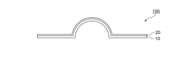
- FIG. 1 is a schematic cross-sectional view of a three-dimensional object derived from a transparent conductive film according to one embodiment of the present invention.
- the three-dimensional object derived from a transparent conductive film 100 includes a substrate 10 and a transparent conductive layer 20 disposed on at least one side of the substrate 10.
- the substrate 10 includes a resin A having a softening point of 200° C. or less.
- the transparent conductive layer 20 also includes metal nanowires (not shown). Although not shown, the transparent conductive film may further include any other appropriate layers.
- the thickness of the transparent conductive film is preferably 10 ⁇ m to 500 ⁇ m, more preferably 15 ⁇ m to 300 ⁇ m, and even more preferably 20 ⁇ m to 200 ⁇ m.
- the sheet resistance of the transparent conductive layer is preferably 3000 ⁇ / ⁇ or less, more preferably 1000 ⁇ / ⁇ or less, and even more preferably 500 ⁇ / ⁇ or less.
- the ratio of the thickness d to the length L of the metal nanowire is preferably 10 to 100,000, more preferably 50 to 100,000, and particularly preferably 100 to 10,000.
- the metal nanowires can be well crossed, and high conductivity can be achieved with a small amount of metal nanowires.
- a three-dimensional molded product derived from a transparent conductive film with high light transmittance can be obtained.
- the "thickness of the metal nanowire” means the diameter when the cross section of the metal nanowire is circular, the short axis when the cross section is elliptical, and the longest diagonal when the cross section is polygonal. The thickness and length of the metal nanowire can be confirmed by a scanning electron microscope or a transmission electron microscope.
- metal constituting the metal nanowires any suitable metal can be used as the metal constituting the metal nanowires, so long as it is a conductive metal.
- metals constituting the metal nanowires include silver, gold, copper, nickel, etc. Materials obtained by plating these metals (e.g., gold plating) may also be used. Among these, silver, copper, or gold are preferred from the viewpoint of conductivity, and silver is more preferred.
- the density of the transparent conductive layer is preferably 1.3 g/cm 3 to 10.5 g/cm 3 , and more preferably 1.5 g/cm 3 to 3.0 g/cm 3. Within such a range, a three-dimensional molded article derived from the transparent conductive film having excellent electrical conductivity and light transmittance can be obtained.
- the metal nanowires in the transparent conductive layer have a fused network structure.
- the metal nanowires having a fused network structure are in a state where the metal nanowires are fused to each other at their contact points.
- the transparent conductive layer containing the metal nanowires having the fused network structure can be formed by applying a metal nanowire dispersion containing the additive, followed by heating and/or pressurization.
- the temperature of the heat treatment is, for example, 50°C to 200°C.
- the transparent conductive layer containing the metal nanowires having the above-mentioned fused network structure may be formed by exposing a coating layer of the metal nanowire dispersion to an acid halide vapor.
- the acid halide vapor include vapors of HCl, HBr, HI, or mixtures thereof.
- any suitable molding method can be used to obtain the transparent substrate, and an appropriate method can be selected from, for example, compression molding, transfer molding, injection molding, extrusion molding, blow molding, powder molding, FRP molding, and solvent casting.
- extrusion molding or solvent casting is preferably used, because it can increase the smoothness of the obtained transparent substrate and obtain good optical uniformity.
- the molding conditions can be set appropriately depending on the composition and type of the resin used.
- the transmittance of the transparent conductive film (that is, the film before three-dimensional molding) and the transparent conductive film after three-dimensional molding (three-dimensional molded article derived from the transparent conductive film) was measured using a spectrophotometer U-4100 manufactured by Hitachi Ltd.
- the three-dimensional object derived from the transparent conductive film was cut into samples in each grid, and the transmittance was measured.
- the mixture was heated to 160° C. for 1 hour or more to react until AgNO 3 was completely reduced, producing silver nanowires.
- acetone was added to the reaction mixture containing the silver nanowires obtained as described above until the volume of the reaction mixture was 5 times that of the reaction mixture, and the reaction mixture was centrifuged (2000 rpm, 20 minutes) to obtain silver nanowires.
- the obtained silver nanowires had a short diameter of 30 nm to 40 nm, a long diameter of 30 nm to 50 nm, and a length of 5 ⁇ m to 50 ⁇ m.
- the silver nanowires (concentration: 0.2% by weight) and pentaethylene glycol dodecyl ether (concentration: 0.1% by weight) were dispersed in pure water to prepare silver nanowire dispersion liquid I.
- Example 1 A polycarbonate-based resin film (manufactured by Teijin Chemicals, product name "PC1151", thickness 100 ⁇ m, softening point: 130° C.) was used as the substrate. The silver nanowire dispersion liquid I was applied to this substrate and dried. Next, as a material for forming the overcoat layer, 80 parts by weight of "Unidic ELS-888" manufactured by DIC Corporation and 20 parts by weight of "Unidic RS28-605" manufactured by DIC Corporation were blended to prepare a resin composition A. This resin composition A was applied to the conductive layer, and ultraviolet light was irradiated at an exposure dose of 230 mJ/cm 2 to form a polymer matrix, thereby obtaining a transparent conductive film. The surface resistance of the transparent conductive film was 30 ⁇ , and the thickness of the transparent conductive layer was 1.0 ⁇ m. The obtained transparent conductive film was subjected to the above-mentioned evaluations, and the results are shown in Table 1.
- the present invention can provide a three-dimensional molded article derived from a transparent conductive film that is excellent in conductivity and appearance, even though it is a three-dimensional molded article derived from a film.
- a substrate with a high softening point when used, it is not possible to mold it into a product with a good appearance (Comparative Examples 1 and 2).
- a conductive layer that is not composed of metal nanowires when provided, the initial resistance is high, and a significant decrease in resistivity is confirmed due to molding (Comparative Examples 3 and 4). In Comparative Example 4, cracks occurred in the conductive layer due to molding.
Landscapes
- Engineering & Computer Science (AREA)
- Chemical & Material Sciences (AREA)
- Organic Chemistry (AREA)
- Theoretical Computer Science (AREA)
- Physics & Mathematics (AREA)
- General Engineering & Computer Science (AREA)
- Wood Science & Technology (AREA)
- Life Sciences & Earth Sciences (AREA)
- Materials Engineering (AREA)
- Dispersion Chemistry (AREA)
- Human Computer Interaction (AREA)
- General Physics & Mathematics (AREA)
- Spectroscopy & Molecular Physics (AREA)
- Inorganic Chemistry (AREA)
- Health & Medical Sciences (AREA)
- Chemical Kinetics & Catalysis (AREA)
- Medicinal Chemistry (AREA)
- Polymers & Plastics (AREA)
- Mechanical Engineering (AREA)
- Non-Insulated Conductors (AREA)
- Laminated Bodies (AREA)
Abstract
Description
1つの実施形態においては、上記金属ナノワイヤが、融着網目構造を有する。
1つの実施形態においては、上記透明導電性フィルム由来立体成形体は、全光線透過率が、80%以上である。
1つの実施形態においては、上記透明導電性フィルム由来立体成形体は、シート抵抗率が、3000Ω/□以下である。
本発明の別の局面においては、透明導電性フィルムが提供される。この透明導電性フィルムは、透明導電性フィルム由来立体成形体を成形する用であり得る。
図1は、本発明の1つの実施形態による透明導電性フィルム由来立体成形体の概略断面図である。透明導電性フィルム由来立体成形体100は、基材10と、基材10の少なくとも片側に配置された透明導電層20とを備える。基材10は、軟化点200℃以下の樹脂Aを含む。また、透明導電層20は、金属ナノワイヤを含む(図示せず)。図示していないが、透明導電性フィルムは、任意の適切なその他の層をさらに含んでいてもよい。
1つの実施形態においては、透明導電層は、金属ナノワイヤおよびポリマーマトリックスを含む。金属ナノワイヤを含む透明導電層を形成すれば、屈曲性に優れ、かつ、光透過率に優れる透明導電性フィルム由来立体成形体を得ることができる。金属ナノワイヤは、ポリマーマトリックスにより保護される。その結果、金属ナノワイヤの腐食が防止され、耐久性により優れる透明導電性フィルム由来立体成形体を得ることができる。
金属ナノワイヤとは、材質が金属であり、形状が針状または糸状であり、径がナノメートルサイズの導電性物質をいう。金属ナノワイヤは直線状であってもよく、曲線状であってもよい。金属ナノワイヤで構成された透明導電層を用いれば、金属ナノワイヤが網の目状となることにより、少量の金属ナノワイヤであっても良好な電気伝導経路を形成することができ、電気抵抗の小さい透明導電性フィルム由来立体成形体を得ることができる。さらに、金属ナノワイヤが網の目状となることにより、網の目の隙間に開口部を形成して、光透過率の高い透明導電性フィルム由来立体成形体を得ることができる。
上記ポリマーマトリックスを構成するポリマーとしては、任意の適切なポリマーが用いられ得る。該ポリマーとしては、例えば、アクリル系ポリマー;ポリエチレンテレフタレート等のポリエステル系ポリマー;ポリスチレン、ポリビニルトルエン、ポリビニルキシレン、ポリイミド、ポリアミド、ポリアミドイミド等の芳香族系ポリマー;ポリウレタン系ポリマー;エポキシ系ポリマー;ポリオレフィン系ポリマー;アクリロニトリル-ブタジエン-スチレン共重合体(ABS);セルロース;シリコン系ポリマー;ポリ塩化ビニル;ポリアセテート;ポリノルボルネン;合成ゴム;フッ素系ポリマー等が挙げられる。好ましくは、ペンタエリスリトールトリアクリレート(PETA)、ネオペンチルグリコールジアクリレート(NPGDA)、ジペンタエリスリトールヘキサアクリレート(DPHA)、ジペンタエリスリトールペンタアクリレート(DPPA)、トリメチロールプロパントリアクリレート(TMPTA)等の多官能アクリレートから構成される硬化型樹脂(好ましくは紫外線硬化型樹脂)が用いられる。
上記透明基材の厚みは、好ましくは8μm~500μmであり、より好ましくは10μm~250μmであり、さらに好ましくは10μm~150μmであり、特に好ましくは15μm~100μmである。
(1)初期抵抗
透明導電性フィルム(すなわち、立体成型前のフィルム)のシート抵抗値を、NAPSON製 商品名「EC-80」を用いて測定した。測定温度は23℃とした。
(2)成型性
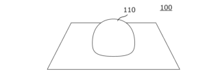
半球状(半径:5cm)窪みを中央に有するブロック状金属製モールドを導電体側の反対の面と向かい合うように合わせ、TOM成型機(布施真空社製)を用いて設定温度160℃で成型を行うことで、半球形状に成型された透明導電性フィルム由来立体成形体を得た。
得られた透明導電性フィルム由来立体成形体の外観により、成型性の良否を評価した。
(3)成型後の抵抗値(シート抵抗値)
透明導電性フィルム(すなわち、立体成型前のフィルム)全面に1cm□の碁盤目を入れた後、上記(2)の方法により立体成型した。
成型後の碁盤目に番号を記載し、それぞれ切り出した。切り出した各部(各番号ごと)において長さが最長となる辺に直行していた辺Aおよび当該辺Aに対向する辺に、銀ペーストを幅3mmで塗布した。銀ペーストを乾燥させた後、テスターで抵抗測定し、シート抵抗値を算出した。
(4)透過率
透明導電性フィルム(すなわち、立体成型前のフィルム)全面に1cm□の碁盤目を入れた後、上記(2)の方法により立体成型した。
透明導電性フィルム(すなわち、立体成型前のフィルム)と立体成型後の透明導電性フィルム(透明導電性フィルム由来立体成形体)の透過率を日立社製の分光光度計U-4100により測定した。
透明導電性フィルム由来立体成形体は、碁盤目ごとに切り出したサンプルについて、透過率を測定した。
攪拌装置を備えた反応容器中、160℃下で、無水エチレングリコール5ml、PtCl2の無水エチレングリコール溶液(濃度:1.5×10⁻⁴mol/L)0.5mlを加えた。4分経過後、得られた溶液に、AgNO3の無水エチレングリコール溶液(濃度:0.12mol/l)2.5mlと、ポリビニルピロリドン(MW:55000)の無水エチレングリコール溶液(濃度:0.36mol/l)5mlとを同時に、6分かけて滴下した。この滴下後、160℃に加熱し1時間以上かけて、AgNO3が完全に還元されるまで反応を行い、銀ナノワイヤを生成した。次いで、上記のようにして得られた銀ナノワイヤを含む反応混合物に、該反応混合物の体積が5倍になるまでアセトンを加えた後、該反応混合物を遠心分離して(2000rpm、20分)、銀ナノワイヤを得た。
得られた銀ナノワイヤは、短径が30nm~40nmであり、長径が30nm~50nmであり、長さは5μm~50μmであった。
純水中に、該銀ナノワイヤ(濃度:0.2重量%)、およびペンタエチレングリコールドデシルエーテル(濃度:0.1重量%)を分散させ、銀ナノワイヤ分散液Iを調製した。
ポリカーボネート系樹脂フィルム(帝人化成社製、製品名「PC1151」、厚み100μm、軟化点:130℃)を基材として用いた。この基材に銀ナノワイヤ分散液Iを塗布・乾燥した。次に、オーバーコート層の形成材料として、DIC(株)製、商品名「ユニディックELS-888」80重量部と、DIC(株)製、商品名「ユニディックRS28-605」20重量とを配合して樹脂組成物Aを調整した。この樹脂組成物Aを導電層に塗布し、紫外線を露光量230mJ/cm2で照射し、ポリマーマトリックスを形成し、透明導電性フィルムを得た。透明導電性フィルムの表面抵抗は、30Ωであり、透明導電層の厚みは1.0μmであった。
得られた透明導電性フィルムを上記評価に供した。結果を表1に示す。
ポリカーボネート系樹脂フィルムに代えて、ナイロンフィルム(三菱化学社製、製品名「スーパーニール」、厚み40μm、軟化点:100℃)を用いたこと以外は、実施例1と同様にして、透明導電性フィルムを得た。得られた透明導電性フィルムを上記評価に供した。結果を表1に示す。
ポリカーボネート系樹脂フィルムに代えて、アクリル系樹脂フィルム(三菱化学社製、製品名「アクリプレン」、厚み40μm、軟化点:100℃)を用いたこと以外は、実施例1と同様にして、透明導電性フィルムを得た。得られた透明導電性フィルムを上記評価に供した。結果を表1に示す。
ポリカーボネート系樹脂フィルムに代えて、PETフィルム(東レ社製、製品名「ルミラー」、厚み40μm、軟化点:210℃)を用いたこと以外は、実施例1と同様にして、透明導電性フィルムを得た。得られた透明導電性フィルムを上記評価に供した。結果を表1に示す。
ポリカーボネート系樹脂フィルムに代えて、シクロオレフィン系樹脂フィルム(日本ゼオン社製、製品名「ZF16」、厚み40μm、軟化点:250℃)を用いたこと以外は、実施例1と同様にして、透明導電性フィルムを得た。得られた透明導電性フィルムを上記評価に供した。結果を表1に示す。
ポリカーボネート系樹脂フィルム(帝人化成社製、製品名「PC1151」、厚み100μm、軟化点:130℃)を基材として用いた。この基材に、ナガセケムテックス社製、製品名「デナトロン」を塗布・乾燥し、PEDOT導電層を備える導電性フィルムを得た。得られた透明導電性フィルムを上記評価に供した。結果を表1に示す。
ポリカーボネート系樹脂フィルム(帝人化成社製、製品名「PC1151」、厚み100μm、軟化点:130℃)を基材として用いた。ITOをターゲットとして当該基材に真空製膜して透明導電性フィルムを得た。得られた透明導電性フィルムを上記評価に供した。結果を表1に示す。

20 透明導電層
100 透明導電性フィルム
Claims (6)
- 基材と、
該基材の少なくとも片側に配置された透明導電層とを備え、
該基材が、軟化点200℃以下の樹脂Aを含み、
該透明導電層が、金属ナノワイヤを含む、
透明導電性フィルム由来立体成形体。 - 前記金属ナノワイヤが、融着網目構造を有する、請求項1に記載の透明導電性フィルム由来立体成形体。
- 全光線透過率が、80%以上である、請求項1または2に記載の透明導電性フィルム由来立体成形体。
- シート抵抗率が、3000Ω/□以下である、請求項1または2に記載の透明導電性フィルム由来立体成形体。
- シート抵抗率が、3000Ω/□以下である、請求項3に記載の透明導電性フィルム由来立体成形体。
- 請求項1から5のいずれかに記載の透明導電性フィルム由来立体成形体を成形する用の、透明導電性フィルム。
Priority Applications (3)
| Application Number | Priority Date | Filing Date | Title |
|---|---|---|---|
| CN202380090599.XA CN120457026A (zh) | 2023-01-04 | 2023-12-12 | 来源于透明导电性膜的立体成形体 |
| KR1020257019224A KR20250133872A (ko) | 2023-01-04 | 2023-12-12 | 투명 도전성 필름 유래 입체 성형체 |
| JP2024568712A JPWO2024147261A1 (ja) | 2023-01-04 | 2023-12-12 |
Applications Claiming Priority (2)
| Application Number | Priority Date | Filing Date | Title |
|---|---|---|---|
| JP2023000205 | 2023-01-04 | ||
| JP2023-000205 | 2023-01-04 |
Publications (1)
| Publication Number | Publication Date |
|---|---|
| WO2024147261A1 true WO2024147261A1 (ja) | 2024-07-11 |
Family
ID=91803790
Family Applications (1)
| Application Number | Title | Priority Date | Filing Date |
|---|---|---|---|
| PCT/JP2023/044346 Ceased WO2024147261A1 (ja) | 2023-01-04 | 2023-12-12 | 透明導電性フィルム由来立体成形体 |
Country Status (5)
| Country | Link |
|---|---|
| JP (1) | JPWO2024147261A1 (ja) |
| KR (1) | KR20250133872A (ja) |
| CN (1) | CN120457026A (ja) |
| TW (1) | TW202439338A (ja) |
| WO (1) | WO2024147261A1 (ja) |
Citations (3)
| Publication number | Priority date | Publication date | Assignee | Title |
|---|---|---|---|---|
| JP2015530693A (ja) * | 2012-06-22 | 2015-10-15 | シー3ナノ・インコーポレイテッドC3Nano Inc. | 金属ナノ構造化網目構造および透明導電性の材料 |
| JP2017090756A (ja) * | 2015-11-13 | 2017-05-25 | 日東電工株式会社 | 光学積層体 |
| WO2022138882A1 (ja) * | 2020-12-24 | 2022-06-30 | 昭和電工株式会社 | 透明導電フィルム積層体 |
Family Cites Families (1)
| Publication number | Priority date | Publication date | Assignee | Title |
|---|---|---|---|---|
| EP3473681B1 (en) | 2005-08-12 | 2020-10-07 | Cambrios Film Solutions Corporation | Nanowires-based transparent conductors |
-
2023
- 2023-12-12 CN CN202380090599.XA patent/CN120457026A/zh active Pending
- 2023-12-12 KR KR1020257019224A patent/KR20250133872A/ko active Pending
- 2023-12-12 JP JP2024568712A patent/JPWO2024147261A1/ja active Pending
- 2023-12-12 WO PCT/JP2023/044346 patent/WO2024147261A1/ja not_active Ceased
- 2023-12-25 TW TW112150563A patent/TW202439338A/zh unknown
Patent Citations (3)
| Publication number | Priority date | Publication date | Assignee | Title |
|---|---|---|---|---|
| JP2015530693A (ja) * | 2012-06-22 | 2015-10-15 | シー3ナノ・インコーポレイテッドC3Nano Inc. | 金属ナノ構造化網目構造および透明導電性の材料 |
| JP2017090756A (ja) * | 2015-11-13 | 2017-05-25 | 日東電工株式会社 | 光学積層体 |
| WO2022138882A1 (ja) * | 2020-12-24 | 2022-06-30 | 昭和電工株式会社 | 透明導電フィルム積層体 |
Also Published As
| Publication number | Publication date |
|---|---|
| TW202439338A (zh) | 2024-10-01 |
| KR20250133872A (ko) | 2025-09-09 |
| CN120457026A (zh) | 2025-08-08 |
| JPWO2024147261A1 (ja) | 2024-07-11 |
Similar Documents
| Publication | Publication Date | Title |
|---|---|---|
| CN104303238B (zh) | 透明导电性墨以及透明导电图案形成方法 | |
| KR20200096852A (ko) | 금속 나노 구조 네트워크 및 투명 전도성 물질 | |
| Tan et al. | Single droplet 3D printing of electrically conductive resin using high aspect ratio silver nanowires | |
| JP2025065234A (ja) | 透明導電性フィルム | |
| CN117954147A (zh) | 透明导电性膜 | |
| JP7663328B2 (ja) | 透明導電性フィルムの製造方法 | |
| TW202439338A (zh) | 由透明導電性膜而來之立體成形體 | |
| JP6712910B2 (ja) | 透明導電性フィルム | |
| JP6792973B2 (ja) | 導電性フィルムおよび導電性フィルムの製造方法 | |
| JP7744120B2 (ja) | 透明導電性フィルム | |
| JP7638882B2 (ja) | 透明導電性フィルムの製造方法 | |
| JP7707334B2 (ja) | 透明導電性フィルム | |
| JP7485629B2 (ja) | 透明導電性フィルム | |
| JP2025116202A (ja) | 透明導電性フィルム | |
| KR20230129923A (ko) | 투명 도전성 필름의 제조 방법 | |
| JP7785453B2 (ja) | 透明導電性フィルムの製造方法 | |
| JP7554122B2 (ja) | 透明導電性フィルム | |
| JP7719722B2 (ja) | 透明導電性フィルムの製造方法 | |
| WO2025100195A1 (ja) | 透明導電性フィルム | |
| TW202203256A (zh) | 導電性膜 | |
| KR20230014685A (ko) | 투명 도전성 필름 |
Legal Events
| Date | Code | Title | Description |
|---|---|---|---|
| 121 | Ep: the epo has been informed by wipo that ep was designated in this application |
Ref document number: 23914749 Country of ref document: EP Kind code of ref document: A1 |
|
| WWE | Wipo information: entry into national phase |
Ref document number: 2024568712 Country of ref document: JP |
|
| WWE | Wipo information: entry into national phase |
Ref document number: 202380090599.X Country of ref document: CN |
|
| NENP | Non-entry into the national phase |
Ref country code: DE |
|
| WWP | Wipo information: published in national office |
Ref document number: 202380090599.X Country of ref document: CN |
|
| 122 | Ep: pct application non-entry in european phase |
Ref document number: 23914749 Country of ref document: EP Kind code of ref document: A1 |