WO2024143251A1 - 伸縮性回路基材及び伸縮性デバイス - Google Patents
伸縮性回路基材及び伸縮性デバイス Download PDFInfo
- Publication number
- WO2024143251A1 WO2024143251A1 PCT/JP2023/046333 JP2023046333W WO2024143251A1 WO 2024143251 A1 WO2024143251 A1 WO 2024143251A1 JP 2023046333 W JP2023046333 W JP 2023046333W WO 2024143251 A1 WO2024143251 A1 WO 2024143251A1
- Authority
- WO
- WIPO (PCT)
- Prior art keywords
- stretchable
- resin
- elastic
- electrical wiring
- substrate
- Prior art date
- Legal status (The legal status is an assumption and is not a legal conclusion. Google has not performed a legal analysis and makes no representation as to the accuracy of the status listed.)
- Ceased
Links
Images






Classifications
-
- H—ELECTRICITY
- H05—ELECTRIC TECHNIQUES NOT OTHERWISE PROVIDED FOR
- H05K—PRINTED CIRCUITS; CASINGS OR CONSTRUCTIONAL DETAILS OF ELECTRIC APPARATUS; MANUFACTURE OF ASSEMBLAGES OF ELECTRICAL COMPONENTS
- H05K1/00—Printed circuits
- H05K1/02—Details
- H05K1/0277—Bendability or stretchability details
- H05K1/0283—Stretchable printed circuits
-
- H—ELECTRICITY
- H05—ELECTRIC TECHNIQUES NOT OTHERWISE PROVIDED FOR
- H05K—PRINTED CIRCUITS; CASINGS OR CONSTRUCTIONAL DETAILS OF ELECTRIC APPARATUS; MANUFACTURE OF ASSEMBLAGES OF ELECTRICAL COMPONENTS
- H05K1/00—Printed circuits
- H05K1/02—Details
-
- H—ELECTRICITY
- H05—ELECTRIC TECHNIQUES NOT OTHERWISE PROVIDED FOR
- H05K—PRINTED CIRCUITS; CASINGS OR CONSTRUCTIONAL DETAILS OF ELECTRIC APPARATUS; MANUFACTURE OF ASSEMBLAGES OF ELECTRICAL COMPONENTS
- H05K1/00—Printed circuits
- H05K1/02—Details
- H05K1/14—Structural association of two or more printed circuits
- H05K1/147—Structural association of two or more printed circuits at least one of the printed circuits being bent or folded, e.g. by using a flexible printed circuit
-
- H—ELECTRICITY
- H05—ELECTRIC TECHNIQUES NOT OTHERWISE PROVIDED FOR
- H05K—PRINTED CIRCUITS; CASINGS OR CONSTRUCTIONAL DETAILS OF ELECTRIC APPARATUS; MANUFACTURE OF ASSEMBLAGES OF ELECTRICAL COMPONENTS
- H05K1/00—Printed circuits
- H05K1/18—Printed circuits structurally associated with non-printed electric components
- H05K1/181—Printed circuits structurally associated with non-printed electric components associated with surface mounted components
-
- H—ELECTRICITY
- H05—ELECTRIC TECHNIQUES NOT OTHERWISE PROVIDED FOR
- H05K—PRINTED CIRCUITS; CASINGS OR CONSTRUCTIONAL DETAILS OF ELECTRIC APPARATUS; MANUFACTURE OF ASSEMBLAGES OF ELECTRICAL COMPONENTS
- H05K1/00—Printed circuits
- H05K1/18—Printed circuits structurally associated with non-printed electric components
- H05K1/189—Printed circuits structurally associated with non-printed electric components characterised by the use of flexible or folded printed circuits
-
- H—ELECTRICITY
- H05—ELECTRIC TECHNIQUES NOT OTHERWISE PROVIDED FOR
- H05K—PRINTED CIRCUITS; CASINGS OR CONSTRUCTIONAL DETAILS OF ELECTRIC APPARATUS; MANUFACTURE OF ASSEMBLAGES OF ELECTRICAL COMPONENTS
- H05K3/00—Apparatus or processes for manufacturing printed circuits
- H05K3/22—Secondary treatment of printed circuits
- H05K3/28—Applying non-metallic protective coatings
- H05K3/284—Applying non-metallic protective coatings for encapsulating mounted components
-
- H—ELECTRICITY
- H05—ELECTRIC TECHNIQUES NOT OTHERWISE PROVIDED FOR
- H05K—PRINTED CIRCUITS; CASINGS OR CONSTRUCTIONAL DETAILS OF ELECTRIC APPARATUS; MANUFACTURE OF ASSEMBLAGES OF ELECTRICAL COMPONENTS
- H05K3/00—Apparatus or processes for manufacturing printed circuits
- H05K3/30—Assembling printed circuits with electric components, e.g. with resistors
- H05K3/32—Assembling printed circuits with electric components, e.g. with resistors electrically connecting electric components or wires to printed circuits
- H05K3/321—Assembling printed circuits with electric components, e.g. with resistors electrically connecting electric components or wires to printed circuits by conductive adhesives
-
- H—ELECTRICITY
- H05—ELECTRIC TECHNIQUES NOT OTHERWISE PROVIDED FOR
- H05K—PRINTED CIRCUITS; CASINGS OR CONSTRUCTIONAL DETAILS OF ELECTRIC APPARATUS; MANUFACTURE OF ASSEMBLAGES OF ELECTRICAL COMPONENTS
- H05K3/00—Apparatus or processes for manufacturing printed circuits
- H05K3/30—Assembling printed circuits with electric components, e.g. with resistors
- H05K3/32—Assembling printed circuits with electric components, e.g. with resistors electrically connecting electric components or wires to printed circuits
- H05K3/321—Assembling printed circuits with electric components, e.g. with resistors electrically connecting electric components or wires to printed circuits by conductive adhesives
- H05K3/323—Assembling printed circuits with electric components, e.g. with resistors electrically connecting electric components or wires to printed circuits by conductive adhesives by applying an anisotropic conductive adhesive layer over an array of pads
-
- H—ELECTRICITY
- H10—SEMICONDUCTOR DEVICES; ELECTRIC SOLID-STATE DEVICES NOT OTHERWISE PROVIDED FOR
- H10W—GENERIC PACKAGES, INTERCONNECTIONS, CONNECTORS OR OTHER CONSTRUCTIONAL DETAILS OF DEVICES COVERED BY CLASS H10
- H10W70/00—Package substrates; Interposers; Redistribution layers [RDL]
- H10W70/60—Insulating or insulated package substrates; Interposers; Redistribution layers
- H10W70/67—Insulating or insulated package substrates; Interposers; Redistribution layers characterised by their insulating layers or insulating parts
- H10W70/69—Insulating materials thereof
Definitions
- FIG. 1 is a plan view conceptually showing an elastic circuit substrate according to the present embodiment, and is a plan view showing an elastic circuit substrate according to a first aspect.
- FIG. 2 is a plan view conceptually showing the elastic circuit substrate according to the present embodiment, and is a plan view showing the elastic circuit substrate according to a second aspect.
- FIG. 2 is a plan view conceptually showing the elastic circuit substrate according to the present embodiment, and is a plan view showing the elastic circuit substrate according to a third aspect.
- FIG. 2 is a cross-sectional view of the elastic circuit substrate shown in FIG. FIG.
- a typical insulating material that can be used is a resin material, and examples of such resins include PET (polyethylene terephthalate), PEN (polyethylene naphthalate), PMMA (polymethyl methacrylate), PI (polyimide), polyamide, PAA (polyacrylic acid), PVA (polyvinyl alcohol), PVC (polyvinyl chloride), polypropylene, polysiloxane, epoxy, glass epoxy, and silicon wafer, and these resins may be used in combination of one or more types. Details will be described later.
- As the material of the non-elastic portion for example, PMMA of about 2.5 GPa, PI of about 3 GPa, and PET film of about 4 GPa can be used. Since Young's modulus depends on the manufacturing method of the material, these Young's modulus values are only a guideline.
- FIG. 1 is a plan view conceptually showing the stretchable circuit substrate according to the present embodiment.
- the stretchable circuit substrate 101 (100) shown in FIG. 1A comprises a stretchable substrate 10, a non-stretchable portion 21 (20) connected to a portion of the outer periphery of the first surface 10aa of the stretchable substrate 10, a first electrical wiring 31A (30A) arranged on the first surface 10aa of the stretchable substrate 10, and a second electrical wiring 31B (30B) arranged on the non-stretchable portion, the first electrical wiring 31A (30A) and the second electrical wiring 31B (30B) being connected, and the stretchable substrate 10 and the non-stretchable portion 21 (20) being connected by a conductive adhesive 40 containing a stretchable resin (hereinafter, sometimes referred to as an "elastic resin-containing conductive adhesive").
- a conductive adhesive 40 containing a stretchable resin hereinafter, sometimes referred to as an "elastic resin-containing conductive adhesive"
- the width of the outer periphery of the stretchable substrate 10 where the non-stretchable portion 20 is disposed can be, for example, about 5 mm to 20 mm, but is not limited to this width.
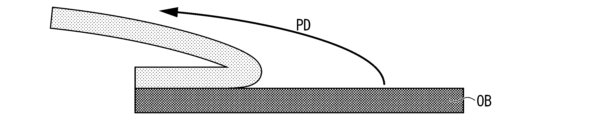
- 3C and 3D are diagrams showing how the non-stretchable portion 20 arranged on the outer periphery of the stretchable substrate 10 is pulled and peeled off from a state in which the stretchable circuit substrate 100 according to the present embodiment (configuration having a non-stretchable portion on the outer periphery of the stretchable substrate) is attached to a receiving body OB (for example, skin, clothing, etc.).
- the symbol PD indicates the peeling direction.
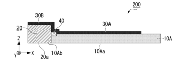
- the non-stretchable portion may be connected to a side portion of the stretchable substrate.
- the stretchable circuit substrate 200 shown in Fig. 4 comprises a stretchable substrate 10A, a non-stretchable portion 20 connected to a portion of the side portion 10Ab of the stretchable substrate 10A, a first electrical wiring 30A arranged on the stretchable substrate 10A, and a second electrical wiring 30B arranged on the non-stretchable portion, the first electrical wiring 30A and the second electrical wiring 30B being connected, and the stretchable substrate 10A and the non-stretchable portion 20 being connected by a stretchable resin-containing conductive adhesive 40.
- the bottom surface 20a of the non-stretchable portion 20 and the bottom surface 10Aa of the stretchable substrate 10A are disposed substantially flush with each other.
- the same components as those in the previous figures have the same functions as those in the previous figures.
- the material used for the elastic substrate 10 is preferably an elastic resin.
- the elastic resin there are no particular limitations on the elastic resin, and any resin known in the art as an elastic resin can be used. Examples include epoxy resins, urethane resins, urea resins, polyurethane urea resins, methacrylic acid resins, polyacrylic resins, silicone resins, diene resins, polyester resins, polyether resins, polyamide resins, and polystyrene resins.
- a stretchable resin substrate in the form of a resin sheet may be used as the stretchable substrate 10.
- a plurality of resin sheets may be laminated to produce a stretchable resin substrate, which may be used as the stretchable substrate 10.
- the stretchable substrate 10 can be formed by applying and solidifying a resin composition containing the resin and a solvent used in the stretchable substrate 10 described above.
- urethane-based resins that can be molded by coating and drying the resin composition without undergoing a curing reaction are preferred. If a resin requires a curing reaction, the composition and degree of curing may vary in the resin sheet if the curing reaction does not proceed uniformly, resulting in a resin sheet that does not have the desired elasticity, strength, and resistance to deterioration over time. Furthermore, when a urethane resin is used, it is preferable that the resin component contains a siloxane bond, because in this case, the resin composition has appropriate water repellency and hydrolysis of the urethane bond is suppressed.
- Z1 is an alkyl group, one or more hydrogen atoms in the alkyl group may be substituted with a cyano group, a carboxy group or a methoxycarbonyl group, and the two or more substituents may be the same or different.
- Z2 is an alkyl group.
- Z3 is an aryl group.
- R4 is a hydrogen atom or a halogen atom.
- the bond marked with the symbol * is formed with the bond destination of the group represented by the general formula (11), (21) or (31).
- the resin component (II) contained in this resin composition has a urethane bond and therefore has high flexibility.
- the resin component (II) is obtained by carrying out a polymerization reaction using a resin having a urethane bond and a polymerizable unsaturated bond, and a RAFT agent for carrying out reversible addition-fragmentation chain transfer polymerization (sometimes abbreviated as "RAFT polymerization” in this specification), which is the origin of the group represented by the general formula (11), (21) or (31).
- RAFT polymerization RAFT polymerization
- the resin component (II) having a group represented by the general formula (11), (21) or (31) has small variation in terms of degree of polymerization and crosslinked state.
- the resin component (II) may have a siloxane bond, in which case the resin composition has a suitable water repellency and the hydrolysis of the urethane bond of the resin component (II) is suppressed.
- Such a resin component (II) is obtained by carrying out a polymerization reaction using a resin having a siloxane bond and a polymerizable unsaturated bond. The method for producing the resin component (II) by RAFT polymerization will be described in detail separately.
- resin component (II) is an oligomer and may be referred to as "resin (a)".
- the resin having a siloxane bond and a polymerizable unsaturated bond used in producing the resin component (II) is an oligomer, and in this embodiment, may be referred to as "resin (b)".
- Resin component (II) is a polymer formed by polymerizing resins (a) together at their polymerizable unsaturated bonds.
- resin component (II) is a polymer formed by polymerizing resins (a) and (b) at their polymerizable unsaturated bonds.
- the resin component (II) preferably has both a urethane bond and a siloxane bond in one molecule.
- the resin (a) is not particularly limited as long as it has a urethane bond and a polymerizable unsaturated bond.
- examples of the resin (a) include those having a urethane bond and a (meth)acryloyl group as a group having a polymerizable unsaturated bond, and more specifically, urethane (meth)acrylates and the like.
- the term "(meth)acrylate” is a concept that includes both "acrylate” and "methacrylate”.
- the resin (b) is not particularly limited as long as it has a siloxane bond and a polymerizable unsaturated bond.
- the resin (b) include various known silicone resins having a (meth)acryloyl group as a group having a polymerizable unsaturated bond, and more specifically, examples of the resin include modified polydialkylsiloxanes in which a (meth)acryloyl group is bonded to one end or both ends of a polydialkylsiloxane such as polydimethylsiloxane.
- Such a resin composition having high solubility is used to form a resin sheet having stretchability, and a stretchable device constructed using this resin sheet has the great advantage of being able to suppress breakage during stretching.
- possible causes of damage to a typical stretchable device during stretching include (i) structural defects such as voids and interfacial peeling caused by shrinkage associated with heat or curing reaction, (ii) hardness unevenness caused by composition unevenness, and (iii) deterioration of materials over time caused by light exposure, oxidation, etc. Therefore, by suppressing structural defects such as voids, interfacial peeling, compositional unevenness, and deterioration of materials over time, damage to the stretchable device when it is stretched can be suppressed.
- the stretchable substrate 10 can be obtained as a resin sheet-like stretchable resin substrate (hereinafter, sometimes referred to as a "resin sheet") by drying and solidifying the resin composition of the specific example.
- a plurality of resin sheets may be laminated to produce the stretchable resin substrate.
- the resin sheet contains the resin component (II) as a main component, and therefore has good elasticity.
- the resin sheet further has a moderate water repellency, and therefore deterioration over time caused by hydrolysis is suppressed.
- the resin sheet having such characteristics is particularly suitable for forming various elastic devices, including wearable devices.
- the resin sheet can be formed simply by solidifying the resin composition through drying, as described above, without undergoing a curing reaction of the resin composition. Therefore, there are no problems associated with performing a curing reaction.
- the resin sheet has areas with different degrees of cure due to heat distribution, it is likely to deteriorate due to repeated expansion and contraction. Furthermore, in both cases of photocuring reaction and thermosetting reaction, it is difficult for the reaction to proceed uniformly in the resin sheet, and in that case, the composition and degree of curing vary in the resin sheet, and the cured resin sheet does not have the desired elasticity and strength. Moreover, since the resin contains a curing agent, it is prone to deterioration over time due to heat and light. In contrast, the resin sheet obtained by drying and solidifying the resin composition of the specific example does not have such a problem.
- the resin sheet can be produced, for example, by applying the resin composition to the desired location and solidifying it by drying, without carrying out a curing reaction.
- the resin composition can be applied by known methods using, for example, various coaters or wire bars, or by various printing methods including inkjet printing.
- the completion of solidification by drying of the resin composition (formation of a resin sheet) can be confirmed, for example, by the fact that no clear change in the mass of the resin composition being dried is observed.
- the stretch rate of the elastic resin substrate can be set appropriately according to the stretch rate required for the elastic circuit substrate.
- the stretch rate can be increased, for example, by increasing the amount of elastic resin. It can also be adjusted by increasing the mol% of bonds with high stretch rates in the resin.
- the stretch rate of the elastic resin substrate can be increased by increasing the ratio of urethane bonds in the resin.
- the non-stretchable portion 20 is made of an insulating material having a Young's modulus of 0.6 kPa or more.
- the non-stretchable portion 20 is made of an insulating material having a Young's modulus twice or more than that of the stretchable substrate 10, preferably an insulating material having a Young's modulus of 5 times or more, more preferably an insulating material having a Young's modulus of 10 times or more, even more preferably an insulating material having a Young's modulus of 20 times or more, even more preferably an insulating material having a Young's modulus of 50 times or more, and even more preferably an insulating material having a Young's modulus of 100 times or more.
- the above resin is preferably soluble in one or more solvents selected from diethylene glycol monobutyl ether acetate (BCA), butyl carbitol (BC), ethyl cyanoacrylate (ECA), ⁇ -terpineol, diethylene glycol monobutyl ether, and diethylene glycol monoethyl ether acetate.
- BCA diethylene glycol monobutyl ether acetate
- BC butyl carbitol
- ECA ethyl cyanoacrylate
- ⁇ -terpineol diethylene glycol monobutyl ether
- diethylene glycol monoethyl ether acetate BCA
- BCA diethylene glycol monobutyl ether acetate
- BC butyl carbitol
- ECA ethyl cyanoacrylate
- ⁇ -terpineol diethylene glycol monobutyl ether
- diethylene glycol monoethyl ether acetate solvents selected from di
- the stretchable electrical wiring 30A of the first embodiment can be formed by applying and solidifying a resin composition containing the resin to be used, metal powder, and a solvent.
- a resin composition containing the resin to be used, metal powder, and a solvent it is preferable to use a dry solidification type resin that can be molded and solidified by simply coating and drying the resin composition without undergoing a curing reaction.
- An example of the dry solidification type resin is a urethane-based resin.
- the stretchable electrical wiring 30A according to the first embodiment can be called a dry solidification type stretchable electrical wiring.
- the resin component contains a siloxane bond, because in this case, the resin composition has appropriate water repellency and hydrolysis of the urethane bond is suppressed.
- the metal powder to be used may be one that has been appropriately produced or a commercially available product.
- a method for producing silver powder includes a method in which a reducing agent-containing aqueous solution is added to an aqueous reaction system containing silver ions to reduce and precipitate silver particles.
- the silver powder may be a silver powder having a silver surface and a metal other than silver inside, such as a silver-coated copper powder.
- Metal powder includes scaly powder.
- scaly powder refers to a powder (metal powder) whose thickness is 1/10 or less of the maximum particle diameter.
- the maximum particle diameter of the scaly powder is defined as follows. The length from end to end of each powder varies depending on the direction in a plan view, and the longest of these lengths is defined as the maximum particle diameter. The maximum particle diameter can be determined by observation with an optical microscope or a scanning electron microscope (SEM) (for example, a visual field of 5000 times), etc.
- SEM scanning electron microscope
- the flake-shaped metal powder may be either a properly manufactured product or a commercially available product.
- flake-shaped metal powder can be produced by forming a thin film of the desired metal and then pulverizing the thin film. Since this method is used to produce the powder by pulverizing the thin film, the individual crushed metal pieces are also flat.
- the thickness relative to the particle size i.e., the degree of flatness
- the breaking elongation of the elastic electrical wiring 30A is 130% or more.
- the breaking elongation is preferably 150% or more, more preferably 200% or more, even more preferably 250% or more, and even more preferably 300% or more.
- the breaking elongation of the elastic electrical wiring 30A can be increased by increasing the proportion of resin contained in the elastic electrical wiring 30A, but an increase in the proportion of resin leads to an increase in resistivity. Therefore, the breaking elongation is appropriately adjusted by adjusting the proportion of resin according to the breaking elongation and resistivity required for the elastic device in which the elastic electrical wiring 30A is used.
- elongation at break is defined as ⁇ (length at break - length before stretching) / length before stretching ⁇ x 100.
- the elongation at break can be measured in each specified direction, but in this specification, "elongation at break of 150% or more" specifies the elongation at break in the direction in which the elongation at break is the greatest. If there is no anisotropy in the elongation at break, the elongation at break will be the same in all directions, and if the anisotropy in the elongation at break is small, the elongation at break will be close in all directions.
- the length of the measurement sample at the time of break is then measured, and the length before pulling (10 mm) is subtracted from the measured length to calculate the breaking elongation of each measurement sample.
- the average value is taken as the breaking elongation, and the breaking elongation rate is calculated according to the above definition.
- the resistance value for each elongation rate is measured by moving the metal substrate by 1 mm at a time to stretch the sample, and the resistance value at the time of elongation is measured each time, and the average value of the six samples is the resistance value R at the time of elongation.
- the thickness of the sheet-like sample of the elastic electrical wiring 30A is measured as follows. A sheet-like sample of the elastic electrical wiring 30A is punched into a circle. Next, the sample is placed on a flat table, and a rectangular PET film with one side larger than the diameter of the circular sample is placed on the sample.
- the thicknesses of the four corners of the rectangular PET film are measured, for example, using a Digimicro ZC-101 (manufactured by Nikon Corporation), and the average is taken as the thickness of the PET film.
- the combined thickness of the sample and the PET film is measured at five points, top, bottom, left, right, and center, and the thickness t of the sample is calculated by subtracting the thickness of the PET film from the average thickness.
- the ratio ( ⁇ 50/ ⁇ 0) of the resistivity ( ⁇ 50 ) at a stretch rate of 50% to the resistivity ( ⁇ 0 ) before stretching is preferably 7 or less, more preferably 6 or less, and even more preferably 5 or less.
- the ratio ( ⁇ 100 / ⁇ 50 ) of the resistivity ( ⁇ 100 ) at a stretch rate of 100% to the resistivity ( ⁇ 50 ) at a stretch rate of 50 % is preferably 8 or less, more preferably 7 or less, even more preferably 6 or less, and even more preferably 5 or less.
- the elastic electrical wiring according to the second aspect contains resin and metal powder, has a breaking elongation rate of 130% or more, has a ratio ( ⁇ 50 / ⁇ 0 ) of the resistivity ( ⁇ 50 ) at a stretch rate of 50% to the resistivity ( ⁇ 0 ) before stretching of 7 or less, contains flake-shaped powder in the metal powder, and has a resin ratio of 8 wt% or more and 20 wt% or less. Explanation of the configuration common to the elastic electrical wiring according to the first aspect will be omitted. Furthermore, the ratio ( ⁇ 100 / ⁇ 50 ) of the resistivity ( ⁇ 100 ) at a stretch rate of 100% to the resistivity ( ⁇ 50 ) at a stretch rate of 50% is preferably 8 or less.
- the resin content in the elastic electrical wiring is preferably 10 wt % or more, and 18 wt % or less.
- the rate of change ( ⁇ 100/ ⁇ 50) of the ratio of the resistivity ( ⁇ 100) at a stretch rate of 100% to the resistivity ( ⁇ 50) at a stretch rate of 50% to the resistivity ( ⁇ 0) before stretching, relative to the ratio ( ⁇ 50/ ⁇ 0) of the resistivity ( ⁇ 50) at a stretch rate of 50% is 140% or less.
- thermosetting reaction is likely to cause shrinkage differences in the elastic electrical wiring due to heat distribution during curing. When such shrinkage differences occur, components made of different materials, such as a device and a sealing material, are likely to peel off at their interfaces.
- the conductive adhesive 40 containing elastic resin may be an elastic resin (resin having elasticity) containing metal powder. Also, a known solder material may be used. The material of the elastic resin-containing conductive adhesive 40 may be an electrical wiring material having elasticity. For example, an elastic resin material containing metal powder (e.g., scale-shaped metal powder) may be used.
- urethane bonds By including urethane bonds in the resin, high flexibility is achieved. Also, when the resin includes either urethane bonds or siloxane bonds, it is possible to achieve both high elasticity and low resistance through the improved dispersion and aggregation of silver powder. Furthermore, when the resin includes both urethane bonds and siloxane bonds, an even greater improvement effect is achieved.
Landscapes
- Engineering & Computer Science (AREA)
- Microelectronics & Electronic Packaging (AREA)
- Manufacturing & Machinery (AREA)
- Structure Of Printed Boards (AREA)
Priority Applications (3)
| Application Number | Priority Date | Filing Date | Title |
|---|---|---|---|
| JP2024567782A JPWO2024143251A1 (https=) | 2022-12-28 | 2023-12-25 | |
| DE112023005394.4T DE112023005394T5 (de) | 2022-12-28 | 2023-12-25 | Dehnbares schaltungssubstrat und dehnbares gerät |
| CN202380088825.0A CN120419294A (zh) | 2022-12-28 | 2023-12-25 | 伸缩性电路基材及伸缩性器件 |
Applications Claiming Priority (2)
| Application Number | Priority Date | Filing Date | Title |
|---|---|---|---|
| JP2022-212027 | 2022-12-28 | ||
| JP2022212027 | 2022-12-28 |
Publications (1)
| Publication Number | Publication Date |
|---|---|
| WO2024143251A1 true WO2024143251A1 (ja) | 2024-07-04 |
Family
ID=91717973
Family Applications (1)
| Application Number | Title | Priority Date | Filing Date |
|---|---|---|---|
| PCT/JP2023/046333 Ceased WO2024143251A1 (ja) | 2022-12-28 | 2023-12-25 | 伸縮性回路基材及び伸縮性デバイス |
Country Status (4)
| Country | Link |
|---|---|
| JP (1) | JPWO2024143251A1 (https=) |
| CN (1) | CN120419294A (https=) |
| DE (1) | DE112023005394T5 (https=) |
| WO (1) | WO2024143251A1 (https=) |
Citations (3)
| Publication number | Priority date | Publication date | Assignee | Title |
|---|---|---|---|---|
| JP2016143763A (ja) * | 2015-02-02 | 2016-08-08 | 株式会社フジクラ | 伸縮性回路基板 |
| JP2016219543A (ja) * | 2015-05-18 | 2016-12-22 | 日本メクトロン株式会社 | 伸縮性配線基板 |
| WO2019093069A1 (ja) * | 2017-11-07 | 2019-05-16 | 大日本印刷株式会社 | 伸縮性回路基板および物品 |
-
2023
- 2023-12-25 WO PCT/JP2023/046333 patent/WO2024143251A1/ja not_active Ceased
- 2023-12-25 CN CN202380088825.0A patent/CN120419294A/zh active Pending
- 2023-12-25 JP JP2024567782A patent/JPWO2024143251A1/ja active Pending
- 2023-12-25 DE DE112023005394.4T patent/DE112023005394T5/de active Pending
Patent Citations (3)
| Publication number | Priority date | Publication date | Assignee | Title |
|---|---|---|---|---|
| JP2016143763A (ja) * | 2015-02-02 | 2016-08-08 | 株式会社フジクラ | 伸縮性回路基板 |
| JP2016219543A (ja) * | 2015-05-18 | 2016-12-22 | 日本メクトロン株式会社 | 伸縮性配線基板 |
| WO2019093069A1 (ja) * | 2017-11-07 | 2019-05-16 | 大日本印刷株式会社 | 伸縮性回路基板および物品 |
Also Published As
| Publication number | Publication date |
|---|---|
| JPWO2024143251A1 (https=) | 2024-07-04 |
| CN120419294A (zh) | 2025-08-01 |
| DE112023005394T5 (de) | 2025-10-09 |
Similar Documents
| Publication | Publication Date | Title |
|---|---|---|
| KR101025128B1 (ko) | 접착제 조성물 및 회로 부재의 접속 구조 | |
| WO2017006652A1 (ja) | 配線回路基板の製造方法 | |
| TW201125083A (en) | Adhesive tape for resin-encapsulating and method of manufacture of resin-encapsulated semiconductor device | |
| WO2017006653A1 (ja) | 配線回路基板 | |
| TW201112267A (en) | Thermosetting electrode paste composition for low temperature | |
| KR20150005516A (ko) | 회로 접속 재료, 회로 접속 구조체, 접착 필름 및 권중체 | |
| CN111336912A (zh) | 一种传感性能可调的柔性应变传感器的制备方法 | |
| JP2008063551A5 (ja) | 電子機器用接着剤組成物、電子機器用接着剤シートおよびそれを用いた電子部品 | |
| WO2021044589A1 (ja) | 離型フィルム及び半導体パッケージの製造方法 | |
| WO2024143251A1 (ja) | 伸縮性回路基材及び伸縮性デバイス | |
| JP7820213B2 (ja) | 伸縮性配線材及び伸縮性デバイス | |
| JP5221574B2 (ja) | セラミックグリーンシート製造用工程フィルム及びその製造方法 | |
| WO2024204601A1 (ja) | 樹脂配線基板および伸縮性デバイス | |
| JP7460692B2 (ja) | フォトレジストフィルム及びその適用 | |
| WO2024204609A1 (ja) | 樹脂配線基板および伸縮性デバイス | |
| WO2024202761A1 (ja) | 樹脂配線基板および伸縮性デバイス | |
| JP7764225B2 (ja) | 太陽電池モジュール | |
| WO2024161901A1 (ja) | 太陽電池モジュール及びそれを備えた電子機器 | |
| WO2024161897A1 (ja) | 太陽電池モジュール及びそれを備えた電子機器 | |
| TW201017045A (en) | High-performance heat dissipation device and method for manufacturing the same | |
| WO2024161899A1 (ja) | 太陽電池モジュール及びそれを備えた電子機器 | |
| WO2024203763A1 (ja) | 伸縮性配線基板及びそれを用いた伸縮性デバイス | |
| WO2025095038A1 (ja) | 樹脂配線基板および伸縮性デバイス | |
| WO2025095037A1 (ja) | 樹脂配線基板および伸縮性デバイス | |
| CN108690521A (zh) | 光学透明双面胶带 |
Legal Events
| Date | Code | Title | Description |
|---|---|---|---|
| 121 | Ep: the epo has been informed by wipo that ep was designated in this application |
Ref document number: 23912031 Country of ref document: EP Kind code of ref document: A1 |
|
| WWE | Wipo information: entry into national phase |
Ref document number: 2024567782 Country of ref document: JP |
|
| WWE | Wipo information: entry into national phase |
Ref document number: 202380088825.0 Country of ref document: CN |
|
| WWE | Wipo information: entry into national phase |
Ref document number: 112023005394 Country of ref document: DE |
|
| WWP | Wipo information: published in national office |
Ref document number: 202380088825.0 Country of ref document: CN |
|
| WWP | Wipo information: published in national office |
Ref document number: 112023005394 Country of ref document: DE |
|
| 122 | Ep: pct application non-entry in european phase |
Ref document number: 23912031 Country of ref document: EP Kind code of ref document: A1 |