WO2024135455A1 - 反射パネル、及び電磁波反射装置 - Google Patents
反射パネル、及び電磁波反射装置 Download PDFInfo
- Publication number
- WO2024135455A1 WO2024135455A1 PCT/JP2023/044426 JP2023044426W WO2024135455A1 WO 2024135455 A1 WO2024135455 A1 WO 2024135455A1 JP 2023044426 W JP2023044426 W JP 2023044426W WO 2024135455 A1 WO2024135455 A1 WO 2024135455A1
- Authority
- WO
- WIPO (PCT)
- Prior art keywords
- panel
- electromagnetic wave
- reflective
- frame
- reflection
- Prior art date
- Legal status (The legal status is an assumption and is not a legal conclusion. Google has not performed a legal analysis and makes no representation as to the accuracy of the status listed.)
- Ceased
Links
Images




Classifications
-
- H—ELECTRICITY
- H01—ELECTRIC ELEMENTS
- H01Q—ANTENNAS, i.e. RADIO AERIALS
- H01Q15/00—Devices for reflection, refraction, diffraction or polarisation of waves radiated from an antenna, e.g. quasi-optical devices
- H01Q15/14—Reflecting surfaces; Equivalent structures
-
- H—ELECTRICITY
- H01—ELECTRIC ELEMENTS
- H01Q—ANTENNAS, i.e. RADIO AERIALS
- H01Q15/00—Devices for reflection, refraction, diffraction or polarisation of waves radiated from an antenna, e.g. quasi-optical devices
- H01Q15/14—Reflecting surfaces; Equivalent structures
- H01Q15/148—Reflecting surfaces; Equivalent structures with means for varying the reflecting properties
-
- H—ELECTRICITY
- H01—ELECTRIC ELEMENTS
- H01Q—ANTENNAS, i.e. RADIO AERIALS
- H01Q15/00—Devices for reflection, refraction, diffraction or polarisation of waves radiated from an antenna, e.g. quasi-optical devices
- H01Q15/14—Reflecting surfaces; Equivalent structures
- H01Q15/18—Reflecting surfaces; Equivalent structures comprising plurality of mutually inclined plane surfaces, e.g. corner reflector
-
- H—ELECTRICITY
- H01—ELECTRIC ELEMENTS
- H01Q—ANTENNAS, i.e. RADIO AERIALS
- H01Q19/00—Combinations of primary active antenna elements and units with secondary devices, e.g. with quasi-optical devices, for giving the antenna a desired directional characteristic
- H01Q19/10—Combinations of primary active antenna elements and units with secondary devices, e.g. with quasi-optical devices, for giving the antenna a desired directional characteristic using reflecting surfaces
- H01Q19/18—Combinations of primary active antenna elements and units with secondary devices, e.g. with quasi-optical devices, for giving the antenna a desired directional characteristic using reflecting surfaces having two or more spaced reflecting surfaces
- H01Q19/185—Combinations of primary active antenna elements and units with secondary devices, e.g. with quasi-optical devices, for giving the antenna a desired directional characteristic using reflecting surfaces having two or more spaced reflecting surfaces wherein the surfaces are plane
Definitions
- the present invention relates to a reflective panel and an electromagnetic wave reflecting device.
- 5G fifth generation
- NLOS non-line-of-sight
- Metasurfaces are formed with periodic structures or patterns that are finer than the wavelength, and are designed to reflect radio waves in a desired direction (see, for example, Non-Patent Document 1). Metasurfaces can achieve a desired reflection angle while maintaining a planar arrangement, so they function effectively as reflectors even in environments where there is not enough space to install many electromagnetic wave reflective panels.
- metasurface reflectors require precise processing of metal layers and resin layers that are smaller than the wavelength of 5G radio waves, and the typical size is about 150 mm to 500 mm on one side.
- specular reflective surfaces it is difficult to bring the electrode reflection efficiency of a metasurface close to 100%.
- metasurface reflectors alone may not be able to sufficiently improve the reflection efficiency and propagation environment.
- reflectors that use specular reflection have many material options for the conductive layer, which is the functional layer, and there are few size restrictions.
- One object of the present invention is to provide a reflection panel and an electromagnetic wave reflection device that combine the advantages of metasurfaces and specular reflection.
- the reflective panel comprises: a first panel that specularly reflects electromagnetic waves in a desired band selected from a frequency band of 1 GHz to 300 GHz; a second panel having a metasurface with controlled reflective properties; and the distance between the first panel and the second panel in a direction perpendicular to the panel surface is 0.0 mm or more and less than 100.0 mm.
- a reflective panel and electromagnetic wave reflecting device that combine the advantages of metasurfaces and specular reflection will be realized.
- FIG. 1 is a schematic diagram of an electromagnetic wave reflection device using a reflection panel of an embodiment.
- FIG. 1 is a schematic diagram of an electromagnetic wave reflecting fence formed by combining multiple electromagnetic wave reflecting devices;
- 13 is a perspective view showing an example of a holding portion that holds a second panel.
- FIG. 4B is a schematic side view of FIG. 4A.
- 13A and 13B are diagrams illustrating another example of a holding portion that holds the second panel.
- 6 is a diagram showing an example of the configuration of a frame used to hold the second panel in FIG. 5 .
- 13A and 13B are diagrams showing a state in which adjacent reflective panels are held by a frame.
- 13A and 13B are diagrams illustrating yet another example of a holding portion that holds the second panel.
- FIG. 1 is a schematic diagram of an electromagnetic wave reflection device using a reflection panel of an embodiment.
- FIG. 1 is a schematic diagram of an electromagnetic wave reflecting fence formed by combining multiple electromagnetic wave reflecting devices;
- 13 is a perspective
- FIG. 2 is a schematic diagram of a layer structure of a first panel.
- FIG. 2 is a schematic plan view of the metasurface of the second panel.
- FIG. 1 is a diagram showing an example of a unit pattern constituting a metasurface.
- FIG. 4 is a schematic diagram of a layer structure of a second panel.
- FIG. 2 shows the analysis space of the second panel.
- a reflective panel that combines the advantages of both a metasurface and specular reflection is realized by combining a first panel that uses specular reflection with a second panel that has a metasurface.
- the first panel that uses specular reflection does not require fine pattern processing, and a large-area panel can be easily manufactured.
- a second panel having a metasurface is disposed on one surface of the first panel.
- the second panel is disposed on the side where the electromagnetic wave enters the first panel, at a predetermined distance from the surface of the first panel, specifically, at a distance of 0.0 mm or more and less than 100.0 mm. As viewed from the electromagnetic wave that enters the first panel, the second panel is located in front of the first panel.
- the second panel is preferably held movably or removably on the incident surface side of the first panel, and the second panel can be attached and its position adjusted on the first panel depending on the installation location of the reflective panel.
- the planar size of the second panel is smaller than that of the first panel, and multiple second panels may be arranged on the incident surface side of the first panel.
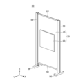
- Fig. 1 is a schematic diagram of an electromagnetic wave reflecting device 60 using a reflecting panel 30 of an embodiment
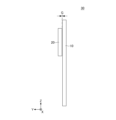
- Fig. 2 is a side view of the reflecting panel 30.
- the plane on which the electromagnetic wave reflecting device 60 is installed is the XY plane
- the height direction perpendicular to the XY plane is the Z direction
- the thickness direction of the reflecting panel 30 is the Y direction.
- the electromagnetic wave reflecting device 60 is installed at a desired location indoors or outdoors, and reflects electromagnetic waves of a predetermined frequency selected from a frequency band of 1 GHz to 300 GHz, for example, 1 GHz to 170 GHz, by the reflecting panel 30.
- the reflective panel 30 has a first panel 10 that uses specular reflection and a second panel 20 that has a metasurface with controlled reflection characteristics, and the gap G between the first panel and the second panel in a direction perpendicular to the panel surface is 0.0 mm or more and less than 100.0 mm.
- the gap G is 0.0 mm
- the second panel 20 is in contact with the surface of the first panel 10.
- the state in which the first panel 10 and the second panel 20 are in contact means a state in which there is no air layer between the two panels that substantially changes the dielectric constant, and the gap due to microscopic unevenness on the panel surface is negligible.
- the metasurface with controlled reflection characteristics reflects the incident electromagnetic wave at a reflection angle different from the angle of incidence.
- the second panel 20 is supported so that it can be moved or removed from the first panel 10.
- the second panel 20 is suspended by a transparent fishing line or polymer wire and placed at a desired position on the surface of the first panel 10 within the range of the gap G mentioned above. Specific examples of the holding configuration of the second panel 20 relative to the first panel 10 will be described later.
- the electromagnetic wave reflection device 60 has a reflection panel 30 and a frame 50 that holds the reflection panel 30.
- the frame 50 holds both ends of the first panel 10 of the reflection panel 30.
- the electromagnetic wave reflection device 60 may further have a top frame 57 that holds the upper end of the reflection panel 30 and a bottom frame 58 that holds the lower end.
- the frame 50, the top frame 57, and the bottom frame 58 hold the entire circumference of the reflection panel 30, more specifically, the entire circumference of the first panel 10.
- the frame 50 may be called a "side frame" because of its positional relationship with the top frame 57 and the bottom frame 58.
- the top frame 57 and the bottom frame 58 are not essential, but by providing the top frame 57 and the bottom frame 58, mechanical strength and safety are ensured during transportation, assembly, and installation of the first panel, and during installation of the second panel 20.
- legs 56 may be provided.
- the legs 56 support the lower end of the frame 50, but the legs 56 may also be connected to a bottom frame 58.
- the legs 56 may be configured to be fixed to the floor or road surface with screws, bolts, etc.
- the legs 56 may be provided with movable parts such as casters to make it movable at the installation location. Without providing the legs 56, the reflection panel 30 may be surrounded entirely by a frame and installed at an angle to a wall, ceiling, floor, etc.
- the second panel 20 of the reflective panel 30 is disposed at a predetermined distance G from the first panel 10 in a direction perpendicular to the panel surface.
- the distance G is set to a range of 0.0 mm or more and less than 100.0 mm from the viewpoint of maintaining a high power reflection efficiency of the reflective panel 30. If the distance G is 100.0 mm or more, reflection, scattering, etc. will occur in the space between the first panel 10 and the second panel 20, reducing the power reflection efficiency of the second panel 20, and as a result, the power reflection efficiency of the entire reflective panel 30 will decrease beyond the allowable range. The reason for this will be described in detail later.
- the second panel 20 may be held in contact with the first panel 10. This is because a thinner air layer between the first panel 10 and the second panel 20 has less effect on the designed reflective properties of the second panel 20.
- FIG 3 is a schematic diagram of an electromagnetic wave reflecting fence 100 in which multiple electromagnetic wave reflecting devices 60 are connected.
- electromagnetic wave reflecting devices 60-1, 60-2, and 60-3 are connected in the horizontal (X) direction by a frame 50.
- the electromagnetic wave reflecting devices 60-1, 60-2, and 60-3 each have a reflecting panel 30-1, 30-2, and 30-3 (which may be collectively referred to as "reflective panel 30" as appropriate).
- second panels 20-1 and 20-2 are attached to the first panels 10-1 and 10-2, respectively.
- the second panels 20-1 and 20-2 may be attached to the same position on the first panels 10-1 and 10-2, or may be attached to different positions, depending on the direction in which the electromagnetic waves arrive and the direction in which they are to be reflected.
- the planar size (length x width) and reflection characteristics of the second panel 20-1 may be the same as or different from the planar size and reflection characteristics of the second panel 20-2.
- the planar size refers to the length x width size.
- the planar size of the first panel 10 refers to the length x width size of the panel.
- the reflection panel 30-3 of the electromagnetic wave reflection device 60-3 is used with the second panel 20 removed, but the second panel 20 may be attached to a desired position on the first panel 10-3, as with the reflection panels 30-1 and 30-2.
- the number of electromagnetic wave reflection devices 60 to be connected is not limited to three, and an electromagnetic wave reflection fence 100 may be assembled with two connected devices, or four or more connected devices.
- Multiple unconnected, independent electromagnetic wave reflecting devices 60 may be arranged in a desired orientation to enclose a desired space.
- a single electromagnetic wave reflecting device 60 may be combined with an electromagnetic wave reflecting fence 100, or two or more electromagnetic wave reflecting fences 100 may be combined to form a specified space. In either case, the second panel 20 can be placed in a desired position on the desired first panel 10.
- Fig. 4A is a perspective view of the reflective panel 30A equipped with a holding portion 31A for holding the second panel 20, and Fig. 4B is a side view of Fig. 4A.
- the holding portion 31A has a first portion 311 movable in a first direction of the first panel 10, and a second portion 312 supporting the second panel 20 and variable in length in a second direction of the first panel 10.
- the first portion 311 is movably attached to a desired position of an edge of the first panel 10.
- the first portion 311 has a hook shape that hooks onto the upper end of the first panel 10 or the top frame 57A, and is slidable in the lateral direction (X direction) of the reflective panel 30A.
- the second part 312 extends from the tip of the first part 311 opposite to the hook and supports the second panel 20.
- the tip of the second part 312 fits into a hole or slit 21 (hereinafter simply referred to as "hole 21") provided in the second panel 20 to support the second panel 20.
- the fitting part between the hole 21 and the second part 312 may be reinforced with adhesive.
- the second part 312 is slidable in the second direction (Z direction in this example) relative to the first part 311, thereby making the length of the holding part 31A variable in the Z direction.
- the second part 312 may be provided with locks or latches at predetermined intervals.
- the first part 311 and the second part 312 are drawn as one-stage sliders, but they may be sliders with two or more stages.
- the second part 312 may be made into a hollow shell configuration, and the rod of the third part may slide inside the second part 312.
- the entire retaining portion 31A is transparent to the wavelengths of electromagnetic waves reflected by the first panel 10 and the second panel 20.
- the first and second portions 311, 312 of the retaining portion 31A preferably have a dielectric constant and a dielectric dissipation factor similar to those of the dielectric layers used in the first and second panels 10, 20, to minimize the effect on the reflective characteristics of the first and second panels 10, 20.
- the adhesive When an adhesive is applied to the mating portion, it is also desirable for the adhesive to have a dielectric constant and a dielectric dissipation factor similar to those of the dielectric layers of the first and second panels 10, 20.
- the holding portion 31A is hooked onto the top frame 57A, but a rail that slidably holds the first portion 311 may be provided on the bottom frame 58 (see Figure 1).
- the second portion 312 supports the second panel 20 from below and extends in the height (+Z) direction.
- the holding portion 31A may be formed to be slidable relative to the frame 50 that holds the side edge of the reflective panel 30A.
- the first portion 311 slides in the vertical direction of the reflective panel 30A, and the second portion 312 expands and contracts in the horizontal direction of the reflective panel 30A.
- the second panel 20 is held movably relative to the first panel 10.
- the gap G between the first panel 10 and the second panel is determined by the thickness of the top frame 57A and the thickness of the first portion 311 of the holding portion 31A.
- the gap that provides the best power reflection efficiency for the frequency used may be measured in advance, and the thickness of the top frame 56A and the thickness of the first portion 311 may be designed.
- FIG. 5 shows the holding portion 31B that holds the second panel 20.
- the holding portion 31B has a first portion 313 that is movable in a first direction of the first panel 10, and a second portion 312 that supports the second panel 20 and has a variable length in the second direction of the first panel 10.
- the first portion 313 has a hook shape that can be slidably hooked onto a slit 522 in a top frame 57B that covers the upper end of the first panel 10.
- the second portion 312 extends from the tip of the first portion 313 opposite the hook, and supports the second panel 20.
- the tip of the second portion 312 fits into a hole 21 provided in the second panel 20 to support the second panel 20.
- the fitting portion between the hole 21 and the second portion 312 may be reinforced with adhesive.
- the second portion 312 is slidable in the height direction (Z direction) relative to the first portion 313, which allows the length of the retaining portion 31B to be variable in the Z direction.
- the second portion 312 may be provided with locks or latches at predetermined intervals.
- the entire retaining portion 31B is transparent to electromagnetic waves reflected by the first panel 10 and the second panel 20.
- the first portion 313 and the second portion 312 of the retaining portion 31A preferably have a dielectric constant and a dielectric dissipation factor similar to those of the dielectric layers used in the first panel 10 and the second panel 20, minimizing the effect on the reflective characteristics of the first panel 10 and the second panel 20.
- the adhesive When an adhesive is applied to the mating portion, it is also desirable for the adhesive to have a dielectric constant and a dielectric dissipation factor similar to those of the dielectric layers of the first panel 10 and the second panel 20.
- the holding portion 31B is hooked onto the slit 522 of the top frame 57B and can slide in the X direction, but the bottom frame 58 may be provided with a rail for sliding the first portion 313, or the first portion 313 may be formed to be slidable relative to the frame 50 that holds the side edge of the reflective panel 30B.
- the holding portion 31B the first panel 10 and the second panel 20 can be transported separately during transportation, and the second panel 20 can be assembled at the desired position relative to the first panel 10 on site.
- FIG. 6 shows an example of the configuration of the top frame 57B.
- the top frame 57B has a main body 520, slits 521 and 522 formed on both sides of the main body 520 in the longitudinal direction, cavities 523 and 524 communicating with the slits 521 and 522, respectively, and grooves 525 and 526 provided in the cavities 523 and 524.
- the upper end of the first panel 10 is inserted into the slit 521 and fixed by fitting it into the groove 525.
- the slit 522 on the opposite side is used as a rail for sliding the first part 313 of the holding part 31B.
- the top frame 57B may have the same shape as the frame 50 that holds adjacent reflective panels 30 together.
- FIG. 7 shows the state in which adjacent first panels 10-1 and 10-2 are held by a frame 50 of the same shape as top frame 57B.
- the first panels 10-1 and 10-2 are inserted all the way into grooves 525 and 526 (see FIG. 6) and stably held.
- at least a portion of the frame 50, particularly the central portion of main body 520 extending between grooves 525 and 526, is made of a good conductor.
- the top frame 57B that receives holding portion 31B may be entirely made of a non-conductor, such as resin.
- the second panel 20 can be held in an adjustable position relative to the first panel 10.
- the first panel 10 and the second panel 20 are transported separately, and the second panel 20 can be assembled at the site in the desired position relative to the first panel 10.
- FIG. 8 shows a holding portion 31C that holds the second panel 20.
- the holding portion 31C has a first portion 315 that is movable in a first direction of the first panel 10, a second portion 312 that extends from the tip of the first portion 315 and has a variable length in the second direction of the first panel 10, and a socket 34 that holds the second panel 20 at the tip of the second portion 312.
- the first portion 315 is movably attached to a desired position on the edge of the first panel 10.
- the first portion 315 has a hook shape that can be slidably hooked into a slit 522 of a top frame 57B that covers the upper end of the first panel 10.
- the second part 312 extends from the tip of the first part 315 opposite the hook, and its length in the longitudinal direction is variable.
- the tip of the second part 312 and the upper end of the second panel 20 are supported by the socket 34.
- the second part 312 is slidable in the height direction (Z direction) relative to the first part 315, which allows the length of the retaining part 31B to be variable in the Z direction.
- Locks or latches may be provided on the second part 312 at predetermined intervals.
- the entire holding portion 31C, including the socket 34, is transparent to electromagnetic waves reflected by the first panel 10 and the second panel 20.
- the first portion 315, the second portion 312, and the socket 34 of the holding portion 31C preferably have a dielectric constant and a dielectric tangent similar to those of the dielectric layers used in the first panel 10 and the second panel 20, minimizing the effect on the reflective characteristics of the first panel 10 and the second panel 20.
- the holding portion 31C is hooked onto the slit 522 of the top frame 57B and can slide in the X direction, but the bottom frame 58 may be provided with a rail for sliding the first portion 315, or the reflective panel 30C may be formed to be slidable relative to the frame 50 that holds the side edge of the reflective panel 30C.
- the holding portion 31C the first panel 10 and the second panel 20 can be transported separately during transportation, and the second panel 20 can be assembled at the desired position relative to the first panel 10 at the site.
- the holding portion 31 is attached using a top frame 57, bottom frame 58, or frame 50 that holds the periphery of the reflective panel 30, but as long as there are no problems with the strength and safety of the reflective panel 30, the holding portion 31 may be attached directly to the edge of the reflective panel 30.
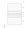
- Fig. 9 shows the layer structure in the thickness direction (Y direction) of the first panel 10.
- the first panel 10 includes a conductive layer 11 and a dielectric layer 14 or 15 bonded to at least one surface of the conductive layer 11 via an adhesive layer 12 or 13.
- the conductive layer 11 is sandwiched between the dielectric layers 14 and 15 via the adhesive layers 12 and 13.
- the conductive layer 11 is a surface that forms the reflective surface of the first panel 10, and is made of a metal material that is suitable for specular reflection. Good conductors such as Cu, Ni, SUS, Ag, and Au can be used as materials for the conductive layer 11.
- the conductive layer 11 has a thickness of 10 ⁇ m or more and 200 ⁇ m or less, preferably 50 ⁇ m or more and 150 ⁇ m or less, so that it can fully function as a reflective surface that specularly reflects electromagnetic waves of the desired frequency.
- the adhesive layers 12 and 13 have a transmittance of 60% or more, preferably 70% or more, and more preferably 80% or more for the frequency used so as to guide the incident electromagnetic waves to the conductive layer 11.
- the adhesive layers 12 and 13 may be formed of vinyl acetate resin, acrylic resin, cellulose resin, aniline resin, ethylene resin, silicone resin, or other resin materials.
- ethylene-vinyl acetate (EVA) copolymer or cycloolefin polymer (COP) may be used.
- the thickness of the adhesive layers 12 and 13 is a thickness that can reliably adhere and hold the dielectric layers 14 and 15 to the conductive layer 11, and is, for example, 10 ⁇ m to 400 ⁇ m.
- the adhesive layers 12 and 13 have a relative dielectric constant and a dielectric loss tangent suitable for achieving the target reflection characteristics of the conductive layer 11.
- the dielectric layers 14 and 15 are insulating polymer films such as polycarbonate, cycloolefin polymer (COP), polyethylene terephthalate (PET), and fluororesin.
- the thicknesses of the dielectric layers 14 and 15 are selected in the range of more than 1.0 mm and less than or equal to 10.0 mm. If the thickness of the conductive layer 11 is 100.0 ⁇ m, the ratio of the thickness of the dielectric layers 14 and 15 to the thickness of the conductive layer 11 is more than 10 and less than or equal to 80.
- the first panel 10 has mechanical strength that can withstand outdoor use and can achieve the target reflection characteristics.
- the ratio of the thickness of the dielectric material to the conductive layer 11 may be increased within a range in which the reflection characteristics are not impaired.
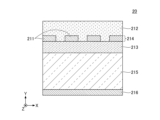
- Figure 10 shows the layer structure in the thickness direction (Y direction) of the second panel 20.
- the second panel 20 has a dielectric layer 215, a conductive layer 214 held on one surface of the dielectric layer 215 by an adhesive layer 213, and a protective layer 212 covering the conductive layer 214.
- the dielectric layer 215 is an insulating polymer film such as polycarbonate, cycloolefin polymer (COP), polyethylene terephthalate (PET), or fluororesin, and has a thickness of about 0.3 mm to 1.0 mm.
- the dielectric layer 215 may be made of any material having a relative dielectric constant and dielectric tangent suitable for achieving the target reflection characteristics.
- a ground layer 216 is formed on the surface of the dielectric layer 215 opposite the conductive layer 214.
- the conductive layer 214 forms a metasurface of the second panel 20, i.e., a surface whose reflection characteristics are artificially controlled.
- the conductive layer 214 has a predetermined pattern formed of metal patches 211 made of a good conductor such as Cu, Ni, Ag, or Au.
- the thickness of the conductive layer 214 is sufficient to reflect incident electromagnetic waves in a designed direction with sufficient strength, and is, for example, 10 ⁇ m to 50 ⁇ m.
- the adhesive layer 213 is a material that can support the metal patches 211 and fix them to the dielectric layer 215, and may be a thermoplastic resin such as vinyl acetate resin, acrylic resin, cellulose resin, or silicone resin.
- the thickness of the adhesive layer 213 is about 5 ⁇ m to 50 ⁇ m.
- the protective layer 212 covering the conductive layer 214 is preferably durable and moisture resistant, and may be made of, for example, ethylene-vinyl acetate (EVA) copolymer or cycloolefin polymer (COP).
- EVA ethylene-vinyl acetate
- COP cycloolefin polymer
- the thickness of the protective layer 212 is 10 ⁇ m to 400 ⁇ m.
- the protective layer 212 may be formed of an adhesive layer, and a dielectric substrate such as polycarbonate may be fixed to the surface of the protective layer 212.
- the reflection characteristics of the reflective panel 30 are evaluated by combining the first panel 10 shown in Fig. 9 with the second panel 20 shown in Fig. 10. It is presumed that the gap G between the first panel 10 and the second panel 20, i.e., the thickness of the air layer, affects the characteristics of the reflective panel 30.
- the gap G is changed in various ways to evaluate the reflection characteristics.
- FIG. 11 shows a model of the conductive pattern used in the conductive layer 214 of the second panel 20.
- the model for evaluating the conductive layer 214 includes a periodic arrangement of unit cells (also called "supercells") 210.
- the unit cells 210 are arranged in 6 rows in the X direction and 36 rows in the Z direction, forming a metasurface that reflects electromagnetic waves at an angle different from the angle of incidence.
- the X direction and Z direction correspond to the X direction and Z direction in FIG. 1.
- FIG. 12 is a schematic diagram showing the configuration of a unit cell 210.
- the unit cell 210 is formed of six metal patches 211a, 211b, 211c, 211d, 211e, and 211f (sometimes collectively referred to as "metal patches 211" as appropriate).
- the metal patches 211a to 211f have the same width (W) and different lengths (L), but the central axes of the lengths (L) are aligned.
- the pitch in the X direction is constant.
- the phase of reflection is controlled by the shape, size, and spacing in the X direction of the metal patches 211a to 211f, and a reflected beam is formed in the desired direction by superimposing the reflected waves. In this example, it is designed so that the peak of the reflected wave of an electromagnetic wave that is perpendicularly incident (incident angle 0°) appears in a direction 50° from the normal line.
- the evaluation method involves holding the second panel 20 shown in Figures 10 to 12 at a predetermined distance G from the first panel 10 in Figure 9.
- a plane wave of 28.0 GHz is incident at an incident angle of 0°, and the scattering cross section of the reflected wave is analyzed.
- the scattering cross section, or radar cross section (RCS) is used as an index of the ability to reflect incident electromagnetic waves.
- the calculated power reflection efficiency needs to be corrected. While the first panel 10 has a specular reflective surface and reflects electromagnetic waves in the same direction for perpendicular incidence, the metasurface of the second panel 20 reflects electromagnetic waves in a direction different from the angle of incidence.
- the power reflection efficiency of the metasurface is the power reflection efficiency calculated from the gain value divided by the correction value. From the perspective of improving the radio wave environment using the reflective panel 30, the power reflection efficiency is 65% or more, preferably 70% or more, and more preferably 75%. If the power reflection efficiency is lower than 65%, it becomes difficult to obtain a sufficient effect of improving the radio wave environment.
- ⁇ is the angle of incidence on the metasurface
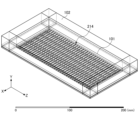
- Figure 13 shows the analysis space 101 for the electromagnetic wave simulation.
- the thickness direction of the layered structure in Figure 10 is the Y direction
- the width direction of the metal patch 211 in the model in Figure 11 is the X direction
- the length direction is the Z direction
- the analysis space 101 is expressed as (size in the X direction) x (size in the Z direction) x (size in the Y direction).
- the size of the analysis space 101 when the frequency of the incident electromagnetic wave is 28.0 GHz is 83.9 mm x 192.6 mm x 3.7 mm.
- the boundary condition is a design in which electromagnetic wave absorbers 102 are placed around the periphery of the analysis space 101.
- Example 1 is Example 1.
- a panel having a planar size of 1.0 m long and 2.0 m wide and a layer structure shown in FIG. 9 is used as the first panel 10.
- a polycarbonate sheet having a length of 1.0 m, a width of 2.0 m and a thickness of 2.0 mm is used as the outermost dielectric layers 14 and 15.
- Two polycarbonate sheets are bonded to both sides of a conductive layer 11 formed of a stainless steel mesh having a thickness of 100 ⁇ m with adhesive layers 12 and 13 of ethylene vinyl acetate having a thickness of 400 ⁇ m.
- the second panel 20 is a panel with a planar size of 0.7 m long and 0.7 m wide, with the layer structure of FIG. 10 and the conductive pattern of FIG. 11.
- a polycarbonate sheet with a length of 0.7 m long, a width of 0.7 m and a thickness of 0.7 mm is used as the dielectric layer 215.
- a ground layer 216 made of an Ag-based multilayer film with a thickness of 0.36 mm is set on one side of the polycarbonate sheet, and a conductive layer 214 including a metal patch 211 made of copper foil with a thickness of 0.03 mm is set on the other side of the polycarbonate sheet via an adhesive layer 213 with a thickness of 0.01 mm.
- a protective layer 212 of EVA with a thickness of 400 ⁇ m is set to cover the conductive layer 214.
- the second panel 20 is disposed with respect to the first panel 10 at a distance G of 0.0 mm.
- the gain value at 50° in the RCS plot peak value of the reflected waveform
- the power reflection efficiency is 77.2%.
- the distance G is 0.0 mm, a high power reflection efficiency exceeding 75% is obtained.
- Example 2 is a second embodiment.
- the configuration and shape of the first panel 10 and the second panel 20 are the same as those of Example 1.
- the second panel 20 is disposed with a distance G of 1.0 mm from the first panel 10.
- the gain value (peak value of the reflected waveform) at 50° in the RCS plot is ⁇ 1.4541 dB.
- the power reflection efficiency is 78.5%.
- the distance G is 1.0 mm, a high power reflection efficiency exceeding 75% is obtained.
- Example 3 is a third embodiment.
- the configuration and shape of the first panel 10 and the second panel 20 are the same as those of Example 1.
- the second panel 20 is disposed with a distance G of 5.0 mm from the first panel 10.
- the gain value (peak value of the reflected waveform) at 50° in the RCS plot is ⁇ 1.7936 dB.
- the power reflection efficiency is 72.6%.
- the distance G is 5.0 mm, a high power reflection efficiency exceeding 70% is obtained.
- Example 4 is a fourth embodiment.
- the configuration and shape of the first panel 10 and the second panel 20 are the same as those of Example 1.
- the second panel 20 is disposed with a distance G of 10.0 mm from the first panel 10.
- the gain value (peak value of the reflected waveform) at 50° in the RCS plot is ⁇ 1.7661 dB.
- the power reflection efficiency is 73.1%.
- the distance G is 10.0 mm, a high power reflection efficiency exceeding 70% is obtained.
- Example 5 is a fifth embodiment.
- the configuration and shape of the first panel 10 and the second panel 20 are the same as those of Example 1.
- the second panel 20 is disposed with a distance G of 20.0 mm from the first panel 10.
- the gain value (peak value of the reflected waveform) at 50° in the RCS plot is ⁇ 1.4887 dB.
- the power reflection efficiency is 77.9%.
- the distance G is 20.0 mm, a high power reflection efficiency exceeding 75% is obtained.
- Example 6 is a sixth embodiment.
- the configuration and shape of the first panel 10 and the second panel 20 are the same as those of Example 1.
- the second panel 20 is disposed with a distance G of 50.0 mm from the first panel 10.
- the gain value (peak value of the reflected waveform) at 50° in the RCS plot is ⁇ 1.8146 dB.
- the power reflection efficiency is 72.3%.
- the distance G is 50.0 mm, a high power reflection efficiency exceeding 70% is obtained.
- Example 7 is a seventh embodiment.
- the configuration and shape of the first panel 10 and the second panel 20 are the same as those of Example 1.
- the second panel 20 is disposed with a distance G of 90.0 mm from the first panel 10.
- the gain value (peak value of the reflected waveform) at 50° in the RCS plot is ⁇ 1.7730 dB.
- the power reflection efficiency is 73.0%.
- the distance G is 90.0 mm, a high power reflection efficiency exceeding 70% is obtained.
- Example 8 is Comparative Example 7.
- the configuration and shape of the first panel 10 and the second panel 20 are the same as those of Example 1.
- the second panel 20 is disposed with a distance G of 100.0 mm from the first panel 10.
- the gain value (peak value of the reflected waveform) at 50° in the RCS plot is ⁇ 2.2818 dB.
- the power reflection efficiency is 64.9%.
- the distance G is 100.0 mm, the power reflection efficiency is less than 65%, and it is difficult to expect a sufficient improvement in the radio wave environment.
- the gap G between the first panel 10 and the second panel 20 in the direction perpendicular to the panel surface of the reflective panel 30 is 0.0 mm or more and less than 100.0 mm.
- the specular reflection first panel 10 is easy to manufacture in a large area, it is possible to hold multiple second panels 20 movably for a first panel 10 of, for example, 3.0 m x 3.0 m.
- a first panel 10 of, for example, 3.0 m x 3.0 m.
- the area where the radio wave propagation environment is improved is expanded with a large-area panel with a power reflection efficiency close to 100%.
- the second panel 20 the radio wave propagation environment can be improved in areas that cannot be covered by specular reflection.
- a windable transparent wire may be used as the second part 312 of the holding part 31, and combined with a transparent hook that serves as the first part. If there is no problem with the mechanical strength and safety of the reflective panel 30, only the top frame 57, the bottom frame 58, or the frame 50 as a side frame may be used.
- the side frame 50 may be used to hold the second panel 20 movably relative to the first panel 10.
- the above disclosure may include the following aspects.
- (Item 1) a first panel that specularly reflects electromagnetic waves in a desired band selected from a frequency band of 1 GHz to 300 GHz; a second panel having a metasurface with controlled reflective properties; and a distance between the first panel and the second panel in a direction perpendicular to the panel surface is 0.0 mm or more and less than 100.0 mm.
- Reflective panel. the second panel is disposed on a side on which the electromagnetic wave is incident on the first panel; Item 2.
- the reflective panel according to item 1. (Item 3)
- the planar size of the second panel is smaller than the planar size of the first panel.
- Item 3. The reflective panel according to item 1 or 2.
- the second panel is movably or removably held relative to the first panel.
- Item 4. The reflective panel according to any one of items 1 to 3.
- (Item 5) a holding portion movably or removably attached to a portion of an edge of the first panel to hold the second panel; 5.
- the holding portion has a first portion movable in a first direction along a first edge of the first panel, and a second portion supporting the second panel and having a variable length in a second direction different from the first direction.
- Item 6. The reflective panel according to item 5.
- a reflective panel that reflects electromagnetic waves in a desired band selected from a frequency band of 1 GHz to 300 GHz; A frame for holding the reflective panel; The reflective panel includes a first panel that specularly reflects the electromagnetic wave and a second panel having a metasurface with controlled reflection characteristics; The distance between the first panel and the second panel in a direction perpendicular to the panel surface of the reflective panel is 0.0 mm or more and less than 100.0 mm.
- Electromagnetic wave reflector. the second panel is disposed on a side on which the electromagnetic wave is incident on the first panel; Item 8.
- An electromagnetic wave reflecting device according to item 7. (Item 9) The planar size of the second panel is smaller than the planar size of the first panel.
- the electromagnetic wave reflecting device according to item 7 or 8.
- the second panel is held movably or removably relative to the first panel.
- Item 10 An electromagnetic wave reflecting device according to any one of items 7 to 9.
- the frame includes a top frame that holds an upper end of the first panel, a side frame that holds a side end of the first panel, or a bottom frame that holds a lower end of the first panel;
- the second panel is held movably or detachably relative to the first panel by utilizing a portion of the top frame, the side frame, or the bottom frame.
- Item 11 An electromagnetic wave reflecting device according to any one of items 7 to 10.
- (Item 12) a holding portion that holds the second panel against the first panel; the holding portion has a first portion movable in a first direction along the top frame, the side frame, or the bottom frame, and a second portion supporting the second panel and having a variable length in a second direction different from the first direction.
- Item 12 An electromagnetic wave reflecting device according to item 11.
- Electromagnetic wave reflecting device 50 Frame (side frame) 56 Legs 57, 57A, 57B Top frame 58 Bottom frame 60, 60-1, 60-2 Electromagnetic wave reflecting device 100 Electromagnetic wave reflecting fence 210 Unit cell 211, 211a to 211f Metal patch 212 Protective layer 213 Adhesive layer 214 Conductive layer 215 Dielectric layer 216 Ground layers 311, 313, 315 First portion 312 Second portion 520 Main body 521, 522 Slits
Landscapes
- Physics & Mathematics (AREA)
- Electromagnetism (AREA)
- Aerials With Secondary Devices (AREA)
Priority Applications (3)
| Application Number | Priority Date | Filing Date | Title |
|---|---|---|---|
| CN202380085599.0A CN120345133A (zh) | 2022-12-21 | 2023-12-12 | 反射面板以及电磁波反射装置 |
| JP2024565832A JPWO2024135455A1 (https=) | 2022-12-21 | 2023-12-12 | |
| US19/238,110 US20250309555A1 (en) | 2022-12-21 | 2025-06-13 | Reflection panel and electromagnetic-wave reflecting apparatus |
Applications Claiming Priority (2)
| Application Number | Priority Date | Filing Date | Title |
|---|---|---|---|
| JP2022-204383 | 2022-12-21 | ||
| JP2022204383 | 2022-12-21 |
Related Child Applications (1)
| Application Number | Title | Priority Date | Filing Date |
|---|---|---|---|
| US19/238,110 Continuation US20250309555A1 (en) | 2022-12-21 | 2025-06-13 | Reflection panel and electromagnetic-wave reflecting apparatus |
Publications (1)
| Publication Number | Publication Date |
|---|---|
| WO2024135455A1 true WO2024135455A1 (ja) | 2024-06-27 |
Family
ID=91588477
Family Applications (1)
| Application Number | Title | Priority Date | Filing Date |
|---|---|---|---|
| PCT/JP2023/044426 Ceased WO2024135455A1 (ja) | 2022-12-21 | 2023-12-12 | 反射パネル、及び電磁波反射装置 |
Country Status (4)
| Country | Link |
|---|---|
| US (1) | US20250309555A1 (https=) |
| JP (1) | JPWO2024135455A1 (https=) |
| CN (1) | CN120345133A (https=) |
| WO (1) | WO2024135455A1 (https=) |
Citations (3)
| Publication number | Priority date | Publication date | Assignee | Title |
|---|---|---|---|---|
| JP2015046846A (ja) * | 2013-08-29 | 2015-03-12 | 日本電信電話株式会社 | アンテナ装置設計方法及びアンテナ装置 |
| WO2021199504A1 (ja) * | 2020-03-31 | 2021-10-07 | Agc株式会社 | 無線伝達システム |
| JP2022108025A (ja) * | 2021-01-12 | 2022-07-25 | 電気興業株式会社 | リフレクトアレー、リフレクトアレーの設計方法、および、リフレクトアレーシステム |
-
2023
- 2023-12-12 WO PCT/JP2023/044426 patent/WO2024135455A1/ja not_active Ceased
- 2023-12-12 CN CN202380085599.0A patent/CN120345133A/zh active Pending
- 2023-12-12 JP JP2024565832A patent/JPWO2024135455A1/ja active Pending
-
2025
- 2025-06-13 US US19/238,110 patent/US20250309555A1/en active Pending
Patent Citations (3)
| Publication number | Priority date | Publication date | Assignee | Title |
|---|---|---|---|---|
| JP2015046846A (ja) * | 2013-08-29 | 2015-03-12 | 日本電信電話株式会社 | アンテナ装置設計方法及びアンテナ装置 |
| WO2021199504A1 (ja) * | 2020-03-31 | 2021-10-07 | Agc株式会社 | 無線伝達システム |
| JP2022108025A (ja) * | 2021-01-12 | 2022-07-25 | 電気興業株式会社 | リフレクトアレー、リフレクトアレーの設計方法、および、リフレクトアレーシステム |
Also Published As
| Publication number | Publication date |
|---|---|
| CN120345133A (zh) | 2025-07-18 |
| JPWO2024135455A1 (https=) | 2024-06-27 |
| US20250309555A1 (en) | 2025-10-02 |
Similar Documents
| Publication | Publication Date | Title |
|---|---|---|
| US12562451B2 (en) | Antenna unit, antenna unit-attached window glass, and matching body | |
| US9444147B2 (en) | Ultra-wide-band (UWB) antenna assembly with at least one director and electromagnetic reflective subassembly and method | |
| US12261367B2 (en) | Antenna unit and window glass | |
| US20200076072A1 (en) | Ebg structure, ebg component, and antenna device | |
| CN116670927A (zh) | 结构体和建筑材料 | |
| US20250055201A1 (en) | Electromagnetic wave reflecting device, electromagnetic wave reflecting fence, and reflection panel | |
| US20220416414A1 (en) | Antenna unit and window glass | |
| US20250309551A1 (en) | Radio transmission system | |
| US20250096480A1 (en) | Electromagnetic wave reflecting device, electromagnetic wave reflecting fence, and reflection panel | |
| US20100001918A1 (en) | Passive repeater antenna | |
| WO2023210566A1 (ja) | 周波数選択反射板 | |
| US20250192444A1 (en) | Electromagnetic wave reflecting device and electromagnetic wave reflecting fence | |
| WO2024135455A1 (ja) | 反射パネル、及び電磁波反射装置 | |
| WO2023003961A1 (en) | Method and system with fragmented metastructures formed with a plurality of metasurface arrays | |
| TW202425422A (zh) | 反射板、使用其之電磁波反射裝置及電磁波反射柵 | |
| JP7673754B2 (ja) | アンテナセット | |
| TW202435511A (zh) | 電波反射體、電波反射體之製作方法、電波反射結構體、電波反射系統及電波反射裝置 | |
| WO2023233885A1 (ja) | 電磁波反射装置、電磁波反射フェンス、及び反射パネル | |
| WO2023233921A1 (ja) | 電磁波反射装置、電磁波反射フェンス、及び反射パネル | |
| WO2024241665A1 (ja) | 電磁波反射パネル、電磁波反射装置、及び電磁波反射フェンス | |
| US20200259270A1 (en) | Technique for Reconstruction of Radiation Patterns for Antennas Working in Close Proximity of Conductive Bodies | |
| WO2025158773A1 (ja) | 電磁波反射パネル、電磁波反射装置、及び電磁波反射フェンス | |
| WO2026058940A1 (ja) | 電波反射体 | |
| JP2026054789A (ja) | ブラインドおよび電波反射方法 | |
| WO2024135216A1 (ja) | 反射パネル、電磁波反射装置、及び電磁波反射フェンス |
Legal Events
| Date | Code | Title | Description |
|---|---|---|---|
| 121 | Ep: the epo has been informed by wipo that ep was designated in this application |
Ref document number: 23906820 Country of ref document: EP Kind code of ref document: A1 |
|
| WWE | Wipo information: entry into national phase |
Ref document number: 2024565832 Country of ref document: JP |
|
| WWE | Wipo information: entry into national phase |
Ref document number: 202380085599.0 Country of ref document: CN |
|
| WWP | Wipo information: published in national office |
Ref document number: 202380085599.0 Country of ref document: CN |
|
| NENP | Non-entry into the national phase |
Ref country code: DE |
|
| 122 | Ep: pct application non-entry in european phase |
Ref document number: 23906820 Country of ref document: EP Kind code of ref document: A1 |