WO2024135356A1 - 半導体装置 - Google Patents
半導体装置 Download PDFInfo
- Publication number
- WO2024135356A1 WO2024135356A1 PCT/JP2023/043583 JP2023043583W WO2024135356A1 WO 2024135356 A1 WO2024135356 A1 WO 2024135356A1 JP 2023043583 W JP2023043583 W JP 2023043583W WO 2024135356 A1 WO2024135356 A1 WO 2024135356A1
- Authority
- WO
- WIPO (PCT)
- Prior art keywords
- die pad
- semiconductor device
- suspension lead
- cross
- extends
- Prior art date
- Legal status (The legal status is an assumption and is not a legal conclusion. Google has not performed a legal analysis and makes no representation as to the accuracy of the status listed.)
- Ceased
Links
Images


Classifications
-
- H—ELECTRICITY
- H10—SEMICONDUCTOR DEVICES; ELECTRIC SOLID-STATE DEVICES NOT OTHERWISE PROVIDED FOR
- H10W—GENERIC PACKAGES, INTERCONNECTIONS, CONNECTORS OR OTHER CONSTRUCTIONAL DETAILS OF DEVICES COVERED BY CLASS H10
- H10W70/00—Package substrates; Interposers; Redistribution layers [RDL]
- H10W70/40—Leadframes
- H10W70/411—Chip-supporting parts, e.g. die pads
-
- H—ELECTRICITY
- H10—SEMICONDUCTOR DEVICES; ELECTRIC SOLID-STATE DEVICES NOT OTHERWISE PROVIDED FOR
- H10W—GENERIC PACKAGES, INTERCONNECTIONS, CONNECTORS OR OTHER CONSTRUCTIONAL DETAILS OF DEVICES COVERED BY CLASS H10
- H10W70/00—Package substrates; Interposers; Redistribution layers [RDL]
- H10W70/40—Leadframes
- H10W70/421—Shapes or dispositions
- H10W70/433—Shapes or dispositions of deformation-absorbing parts, e.g. leads having meandering shapes
-
- H—ELECTRICITY
- H10—SEMICONDUCTOR DEVICES; ELECTRIC SOLID-STATE DEVICES NOT OTHERWISE PROVIDED FOR
- H10W—GENERIC PACKAGES, INTERCONNECTIONS, CONNECTORS OR OTHER CONSTRUCTIONAL DETAILS OF DEVICES COVERED BY CLASS H10
- H10W70/00—Package substrates; Interposers; Redistribution layers [RDL]
- H10W70/40—Leadframes
- H10W70/481—Leadframes for devices being provided for in groups H10D8/00 - H10D48/00
-
- H—ELECTRICITY
- H10—SEMICONDUCTOR DEVICES; ELECTRIC SOLID-STATE DEVICES NOT OTHERWISE PROVIDED FOR
- H10W—GENERIC PACKAGES, INTERCONNECTIONS, CONNECTORS OR OTHER CONSTRUCTIONAL DETAILS OF DEVICES COVERED BY CLASS H10
- H10W70/00—Package substrates; Interposers; Redistribution layers [RDL]
- H10W70/60—Insulating or insulated package substrates; Interposers; Redistribution layers
-
- H—ELECTRICITY
- H10—SEMICONDUCTOR DEVICES; ELECTRIC SOLID-STATE DEVICES NOT OTHERWISE PROVIDED FOR
- H10W—GENERIC PACKAGES, INTERCONNECTIONS, CONNECTORS OR OTHER CONSTRUCTIONAL DETAILS OF DEVICES COVERED BY CLASS H10
- H10W72/00—Interconnections or connectors in packages
-
- H—ELECTRICITY
- H10—SEMICONDUCTOR DEVICES; ELECTRIC SOLID-STATE DEVICES NOT OTHERWISE PROVIDED FOR
- H10W—GENERIC PACKAGES, INTERCONNECTIONS, CONNECTORS OR OTHER CONSTRUCTIONAL DETAILS OF DEVICES COVERED BY CLASS H10
- H10W74/00—Encapsulations, e.g. protective coatings
- H10W74/10—Encapsulations, e.g. protective coatings characterised by their shape or disposition
- H10W74/111—Encapsulations, e.g. protective coatings characterised by their shape or disposition the semiconductor body being completely enclosed
- H10W74/114—Encapsulations, e.g. protective coatings characterised by their shape or disposition the semiconductor body being completely enclosed by a substrate and the encapsulations
-
- H—ELECTRICITY
- H10—SEMICONDUCTOR DEVICES; ELECTRIC SOLID-STATE DEVICES NOT OTHERWISE PROVIDED FOR
- H10W—GENERIC PACKAGES, INTERCONNECTIONS, CONNECTORS OR OTHER CONSTRUCTIONAL DETAILS OF DEVICES COVERED BY CLASS H10
- H10W90/00—Package configurations
-
- H—ELECTRICITY
- H10—SEMICONDUCTOR DEVICES; ELECTRIC SOLID-STATE DEVICES NOT OTHERWISE PROVIDED FOR
- H10W—GENERIC PACKAGES, INTERCONNECTIONS, CONNECTORS OR OTHER CONSTRUCTIONAL DETAILS OF DEVICES COVERED BY CLASS H10
- H10W90/00—Package configurations
- H10W90/811—Multiple chips on leadframes
-
- H—ELECTRICITY
- H10—SEMICONDUCTOR DEVICES; ELECTRIC SOLID-STATE DEVICES NOT OTHERWISE PROVIDED FOR
- H10W—GENERIC PACKAGES, INTERCONNECTIONS, CONNECTORS OR OTHER CONSTRUCTIONAL DETAILS OF DEVICES COVERED BY CLASS H10
- H10W72/00—Interconnections or connectors in packages
- H10W72/851—Dispositions of multiple connectors or interconnections
- H10W72/874—On different surfaces
- H10W72/884—Die-attach connectors and bond wires
-
- H—ELECTRICITY
- H10—SEMICONDUCTOR DEVICES; ELECTRIC SOLID-STATE DEVICES NOT OTHERWISE PROVIDED FOR
- H10W—GENERIC PACKAGES, INTERCONNECTIONS, CONNECTORS OR OTHER CONSTRUCTIONAL DETAILS OF DEVICES COVERED BY CLASS H10
- H10W90/00—Package configurations
- H10W90/701—Package configurations characterised by the relative positions of pads or connectors relative to package parts
- H10W90/731—Package configurations characterised by the relative positions of pads or connectors relative to package parts of die-attach connectors
- H10W90/736—Package configurations characterised by the relative positions of pads or connectors relative to package parts of die-attach connectors between a chip and a stacked lead frame, conducting package substrate or heat sink
-
- H—ELECTRICITY
- H10—SEMICONDUCTOR DEVICES; ELECTRIC SOLID-STATE DEVICES NOT OTHERWISE PROVIDED FOR
- H10W—GENERIC PACKAGES, INTERCONNECTIONS, CONNECTORS OR OTHER CONSTRUCTIONAL DETAILS OF DEVICES COVERED BY CLASS H10
- H10W90/00—Package configurations
- H10W90/701—Package configurations characterised by the relative positions of pads or connectors relative to package parts
- H10W90/751—Package configurations characterised by the relative positions of pads or connectors relative to package parts of bond wires
- H10W90/756—Package configurations characterised by the relative positions of pads or connectors relative to package parts of bond wires between a chip and a stacked lead frame, conducting package substrate or heat sink
Definitions
- This disclosure relates to a semiconductor device.
- the semiconductor device disclosed in Patent Document 1 includes two die pads, and a control element (controller) and a drive element (gate driver) mounted individually on the two die pads.
- the semiconductor device drives switching elements such as IGBTs and MOSFETs.
- the semiconductor device is used in inverter circuits, etc.
- the power supply voltage supplied to the drive element is equal to or greater than the voltage applied to the switching element, so the power supply voltage supplied to the control element is different from the power supply voltage supplied to the drive element. This results in a difference between the voltage applied to the control element and its conductive path, and the voltage applied to the drive element and its conductive path. Therefore, in this semiconductor device, an insulating element is interposed in the transmission path of the electrical signal between the control element and drive element, so that the control element and its conductive path are insulated from the drive element and its conductive path. This prevents dielectric breakdown of each of the control element and drive element.
- the semiconductor device includes two suspension leads connected to the die pad on which the control element and insulating element are mounted, an intermediate lead that is conductive to the control element, and a sealing resin that covers the two die pads, the control element, the drive element, and the insulating element.
- the two suspension leads are exposed to the outside from the same side of the sealing resin as the side on which the intermediate leads are exposed to the outside.
- a load from a bonding tool or the like acts on the die pad to which the two suspension leads are connected. This causes bending in each of the two suspension leads, and causes deflection in the same direction as the load. If the deflection caused in each of the two suspension leads is larger, the inclination of the die pad connected to the two suspension leads becomes larger. This may result in a decrease in the bonding strength of the control element and insulating element to the die pad, or cause poor bonding of the wires that are conductively bonded to these elements.
- An object of the present disclosure is to provide a semiconductor device that is an improvement over conventional semiconductor devices.
- an object of the present disclosure is to provide a semiconductor device that is capable of stabilizing the position of the die pad during manufacturing.
- the semiconductor device provided by the first aspect of the present disclosure includes a first die pad, a first suspension lead connected to one side of the first die pad in a first direction, a second suspension lead located on the opposite side of the first die pad from the first suspension lead and connected to the first die pad, a first semiconductor element mounted on the first die pad, and a sealing resin covering the first die pad and the first semiconductor element.
- the sealing resin has two first side surfaces facing opposite each other in the first direction and a second side surface facing a second direction perpendicular to the first direction. Each of the first suspension lead and the second suspension lead is spaced apart from the two first side surfaces and exposed to the outside from the second side surface.
- the first suspension lead has a first inner portion covered by the sealing resin and a first outer portion connected to the first inner portion and exposed to the outside.
- the first die pad has a first edge extending in the first direction and located closest to the second side surface.
- the first inner part includes a first part extending from a boundary with an extension line of the first edge to the first die pad.
- the cross-sectional area of the first part in the direction in which it extends is greater than any cross-sectional area of the first outer part in the direction in which it extends.
- the above configuration makes it possible to stabilize the position of the die pad during the manufacture of semiconductor devices.
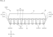
- FIG. 1 is a plan view of a semiconductor device according to a first embodiment of the present disclosure.
- FIG. 2 is a plan view corresponding to FIG. 1, seen through the sealing resin.
- FIG. 3 is a front view of the semiconductor device shown in FIG.
- FIG. 4 is a left side view of the semiconductor device shown in FIG.
- FIG. 5 is a right side view of the semiconductor device shown in FIG.
- FIG. 6 is a cross-sectional view taken along line VI-VI in FIG.
- FIG. 7 is a cross-sectional view taken along line VII-VII in FIG.
- FIG. 8 is a cross-sectional view taken along line VIII-VIII in FIG.
- FIG. 9 is a partially enlarged view of FIG. FIG.
- FIG. 10A is a cross-sectional view taken along line XA-XA in FIG.
- FIG. 10B is a cross-sectional view taken along line XB-XB in FIG.
- FIG. 10C is a cross-sectional view taken along line XC-XC in FIG.
- FIG. 11A is a cross-sectional view of the second inner portion of the second suspension lead in the direction in which the second inner portion extends.
- FIG. 11B is a cross-sectional view of the second outer part of the second suspension lead in the direction in which it extends.
- FIG. 12A is a cross-sectional view of the third inner portion of the third suspension lead in the direction in which the third inner portion extends.
- FIG. 12B is a cross-sectional view of the third outer part of the third suspension lead in the direction in which it extends.
- FIG. 13 is a plan view of a semiconductor device according to a second embodiment of the present disclosure.
- FIG. 14 is a plan view corresponding to FIG. 13, seen through the sealing resin.
- 15 is a rear view of the semiconductor device shown in FIG. 16 is a left side view of the semiconductor device shown in FIG.
- FIG. 17 is a plan view of a lead frame used in the manufacture of the semiconductor device shown in FIG.
- FIG. 18 is a partially enlarged view of FIG.
- FIG. 19A is a cross-sectional view taken along line XIXA-XIXA in FIG. FIG.
- FIG. 19B is a cross-sectional view taken along line XIXB-XIXB in FIG.
- FIG. 19C is a cross-sectional view taken along line XIXC-XIXC in FIG.
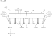
- FIG. 20 is a plan view of a semiconductor device according to a third embodiment of the present disclosure.
- FIG. 21 is a plan view corresponding to FIG. 20, seen through the sealing resin.
- 22 is a left side view of the semiconductor device shown in FIG. 20.
- FIG. 23 is a right side view of the semiconductor device shown in FIG. 20.
- FIG. FIG. 24 is a partially enlarged view of FIG.
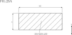
- FIG. 25A is a cross-sectional view taken along line XXVA-XXVA in FIG. 24.
- FIG. 25B is a cross-sectional view taken along line XXVB-XXVB in FIG.
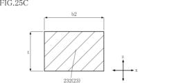
- FIG. 25C is a cross-sectional view taken along line XXVC-XXVC in FIG. 24.
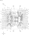
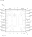
- the semiconductor device A10 includes a first semiconductor element 11, a second semiconductor element 12, an insulating element 13, a first die pad 21, a second die pad 22, a first suspension lead 23, a second suspension lead 24, a third suspension lead 25, a fourth suspension lead 26, a plurality of first intermediate leads 31, a plurality of second intermediate leads 32, and a sealing resin 50.
- the semiconductor device A10 further includes two side leads 27, a plurality of first wires 41, a plurality of second wires 42, a plurality of third wires 43, and a plurality of fourth wires 44.
- the semiconductor device A10 is surface-mounted on a wiring board of an inverter device of an electric vehicle or a hybrid vehicle, for example.
- the package format of the semiconductor device A10 is a small outline package (SOP).
- SOP small outline package
- FIG. 2 shows the sealing resin 50 through the transparent state.
- the outer shape of the sealing resin 50 is indicated by an imaginary line (two-dot chain line).
- the direction perpendicular to the normal direction of the first mounting surface 21A of the first die pad 21 described later is called the "first direction x”.
- One direction perpendicular to the first direction x is called the “second direction y”.
- the direction perpendicular to both the first direction x and the second direction y is called the "third direction z”.
- the third direction z corresponds to the normal direction of the first mounting surface 21A of the first die pad 21.
- the first semiconductor element 11, the second semiconductor element 12, and the insulating element 13 are each composed of individual elements.
- the second semiconductor element 12 is located on the opposite side of the first semiconductor element 11 in the second direction y with the insulating element 13 as a reference.
- the insulating element 13 is located next to the first semiconductor element 11 in the first direction x.
- each of the first semiconductor element 11, the second semiconductor element 12, and the insulating element 13 is rectangular with its longer side extending in the first direction x.
- the first semiconductor element 11 controls the second semiconductor element 12.
- the first semiconductor element 11 includes a circuit that converts an electrical signal input from another semiconductor device into a PWM control signal, a transmission circuit that transmits the PWM control signal to the second semiconductor element 12, and a receiving circuit that receives the electrical signal from the second semiconductor element 12.
- the second semiconductor element 12 drives a switching element located outside the semiconductor device A10.
- the switching element is, for example, an IGBT (Insulated Gate Bipolar Transistor) or a MOSFET (Metal-Oxide-Semiconductor Field-Effect Transistor).
- the second semiconductor element 12 includes a receiving circuit for receiving a PWM control signal, a circuit for driving the switching element based on the PWM control signal, and a transmitting circuit for transmitting an electrical signal to the first semiconductor element 11.
- An example of the electrical signal is an output signal from a temperature sensor located near the motor.
- the insulating element 13 transmits an electric signal such as a PWM (Pulse Width Modulation) control signal in an insulated state.
- the insulating element 13 is an inductor-coupled type.
- An insulating transformer is an example of an inductor-coupled type insulating element 13.
- the insulating transformer transmits an electric signal in an insulated state by inductively coupling two inductors (coils).
- the two inductors include a transmitting inductor and a receiving inductor. Each of the two inductors is stacked in the third direction z.
- a dielectric layer made of silicon dioxide (SiO 2 ) or the like is located between the transmitting inductor and the receiving inductor. The dielectric layer electrically insulates the transmitting inductor and the receiving inductor.
- the insulating element 13 may be a capacitive type.
- a capacitor is an example of a capacitive type insulating element 13.
- the voltages applied to the first semiconductor element 11 and the second semiconductor element 12 are different from each other. Therefore, a potential difference occurs between the first semiconductor element 11 and the second semiconductor element 12.
- the voltage applied to the second semiconductor element 12 is higher than the voltage applied to the first semiconductor element 11.
- the power supply voltage supplied to the second semiconductor element 12 is higher than the power supply voltage supplied to the first semiconductor element 11.
- the first circuit including the first semiconductor element 11 and the second circuit including the second semiconductor element 12 are insulated from each other by the insulating element 13.
- the insulating element 13 is conductive between the first circuit and the second circuit.
- the first circuit includes a first suspension lead 23, a second suspension lead 24, and a plurality of first intermediate leads 31.
- the second circuit includes a third suspension lead 25, a fourth suspension lead 26, and a plurality of second intermediate leads 32.
- the first circuit and the second circuit have relatively different potentials.
- the potential of the first circuit is higher than the potential of the second circuit.
- the insulating element 13 then relays mutual signals between the first circuit and the second circuit.
- the voltage applied to the ground (GND) of the first semiconductor element 11 is about 0 V
- the voltage applied to the ground of the second semiconductor element 12 may transiently reach 600 V or more.
- the first semiconductor element 11 has a plurality of first electrodes 111.
- the plurality of first electrodes 111 are provided on the upper surface of the first semiconductor element 11 (the surface facing the same side as the first mounting surface 21A of the first die pad 21 described below).
- the plurality of first electrodes 111 include, for example, aluminum (Al).
- the plurality of first electrodes 111 are electrically connected to a circuit configured in the first semiconductor element 11.
- the second semiconductor element 12 has a plurality of second electrodes 121.
- the plurality of second electrodes 121 are provided on the upper surface of the second semiconductor element 12 (the surface facing the same side as the second mounting surface 22A of the second die pad 22 described later).
- the plurality of second electrodes 121 include, for example, aluminum.
- the plurality of second electrodes 121 are electrically connected to a circuit configured in the second semiconductor element 12.
- the insulating element 13 is located between the second semiconductor element 12 and the first semiconductor element 11 in the third direction z. Therefore, the first semiconductor element 11 is located on the opposite side to the second semiconductor element 12 with respect to the insulating element 13 in the second direction y.
- a plurality of third electrodes 131 and a plurality of fourth electrodes 132 are provided on the upper surface of the insulating element 13 (the surface facing the same side as the first mounting surface 21A of the first die pad 21 described later). Each of the plurality of third electrodes 131 and the plurality of fourth electrodes 132 is conductive to either the transmitting inductor or the receiving inductor.
- the plurality of third electrodes 131 are arranged along the first direction x, and are located between the first semiconductor element 11 and the second semiconductor element 12 in the second direction y.
- the plurality of fourth electrodes 132 are arranged along the first direction x, and are located on the opposite side to the first semiconductor element 11 with respect to the plurality of third electrodes 131 in the second direction y.
- the multiple third electrodes 131 and the multiple fourth electrodes 132 include, for example, aluminum.
- the sealing resin 50 covers the first semiconductor element 11, the second semiconductor element 12, the insulating element 13, the first die pad 21, and the second die pad 22. As shown in FIG. 6, the sealing resin 50 further covers the first wires 41, the second wires 42, the third wires 43, and the fourth wires 44.
- the sealing resin 50 is an insulator.
- the sealing resin 50 is made of a material that contains, for example, epoxy resin. When viewed in the third direction z, the sealing resin 50 is rectangular.
- the sealing resin 50 has a top surface 51, a bottom surface 52, two first side surfaces 53, a second side surface 54, and a third side surface 55.
- the top surface 51 and the bottom surface 52 face in opposite directions in the third direction z.
- Each of the top surface 51 and the bottom surface 52 is flat (or approximately flat).
- the two first side surfaces 53 are connected to the top surface 51 and the bottom surface 52 and face opposite each other in the first direction x.
- Each of the two first side surfaces 53 includes a first upper portion 531, a first lower portion 532, and a first intermediate portion 533.
- the first upper portion 531 is connected to the top surface 51 on one side in the third direction z and to the first intermediate portion 533 on the other side in the third direction z.
- the first upper portion 531 is inclined with respect to the top surface 51.
- the first lower portion 532 is connected to the bottom surface 52 on one side in the third direction z and to the first intermediate portion 533 on the other side in the third direction z.
- the first lower portion 532 is inclined with respect to the bottom surface 52.
- the first intermediate portion 533 is located between the first upper portion 531 and the first lower portion 532 in the third direction z.
- the in-plane direction of the first intermediate portion 533 includes the third direction z. When viewed in the third direction z, the first intermediate portion 533 is located outward from the top surface 51 and the bottom surface 52.
- the second side 54 is connected to the top surface 51 and the bottom surface 52 and faces one side in the second direction y.
- the second side 54 is located closer to the first die pad 21 than the third side 55.
- the second side 54 includes a second upper portion 541, a second lower portion 542, and a second intermediate portion 543.
- the second upper portion 541 is connected to the top surface 51 on one side in the third direction z and to the second intermediate portion 543 on the other side in the third direction z.
- the second upper portion 541 is inclined with respect to the top surface 51.
- the second lower portion 542 is connected to the bottom surface 52 on one side in the third direction z and to the second intermediate portion 543 on the other side in the third direction z.
- the second lower portion 542 is inclined with respect to the bottom surface 52.
- the second intermediate portion 543 is located between the second upper portion 541 and the second lower portion 542 in the third direction z.
- the in-plane direction of the second intermediate portion 543 includes the third direction z. When viewed in the third direction z, the second intermediate portion 543 is located outward from the top surface 51 and the bottom surface 52.
- the third side 55 is connected to the top surface 51 and the bottom surface 52 and faces the opposite side to the second side 54 in the second direction y.
- the third side 55 is located closer to the second die pad 22 than the second side 54.
- the third side 55 includes a third upper portion 551, a third lower portion 552, and a third intermediate portion 553.
- the third upper portion 551 is connected to the top surface 51 on one side in the third direction z and to the third intermediate portion 553 on the other side in the third direction z.
- the third upper portion 551 is inclined with respect to the top surface 51.
- the third lower portion 552 is connected to the bottom surface 52 on one side in the third direction z and to the third intermediate portion 553 on the other side in the third direction z.
- the third lower portion 552 is inclined with respect to the bottom surface 52.
- the third intermediate portion 553 is located between the third upper portion 551 and the third lower portion 552 in the third direction z.
- the in-plane direction of the third intermediate portion 553 includes the third direction z. When viewed in the third direction z, the third intermediate portion 553 is located outward from the top surface 51 and the bottom surface 52.
- the first die pad 21, the second die pad 22, the first suspension lead 23, the second suspension lead 24, the third suspension lead 25, the fourth suspension lead 26, the two side leads 27, the multiple first intermediate leads 31, and the multiple second intermediate leads 32 all contain copper (Cu).
- the first die pad 21 and the second die pad 22 are spaced apart from each other in the second direction y, as shown in Figures 1 and 2.
- the first semiconductor element 11 and the insulating element 13 are mounted on the first die pad 21, and the second semiconductor element 12 is mounted on the second die pad 22.
- the area of the first die pad 21 is larger than the area of the second die pad 22 when viewed in the third direction z.
- the first semiconductor element 11 may be mounted on the first die pad 21, and the second semiconductor element 12 and the insulating element 13 may be mounted on the second die pad 22.
- the first die pad 21 has a first mounting surface 21A facing one side in the third direction z.
- the first semiconductor element 11 and the insulating element 13 are each bonded to the first mounting surface 21A via a bonding layer 29.
- the bonding layer 29 is made of a paste containing metal particles.
- the metal particles are, for example, silver (Ag). Therefore, the bonding layer 29 is a conductor. Alternatively, the bonding layer 29 may be solder.
- the first die pad 21 is covered with a sealing resin 50.
- the first die pad 21 has two first holes 211, a plurality of second holes 212, and two third holes 213.
- the two first holes 211, the plurality of second holes 212, and the two third holes 213 each penetrate the first die pad 21 in the third direction z.
- the two first holes 211 are located on both sides of the first semiconductor element 11 in the first direction x.
- Each of the two first holes 211 extends in the second direction y.
- the plurality of second holes 212 are located between the first semiconductor element 11 and the insulating element 13 in the second direction y.
- Each of the plurality of second holes 212 extends in the first direction x.
- the plurality of second holes 212 are arranged along the first direction x.
- the two third holes 213 are located on both sides of the insulating element 13 in the first direction x.
- Each of the two third holes 213 extends in the second direction y.
- the first suspension lead 23 is connected to one side of the first die pad 21 in the first direction x.
- the first suspension lead 23 is separated from the two first side surfaces 53 of the sealing resin 50.
- the first suspension lead 23 is exposed to the outside from the second side surface 54 of the sealing resin 50.
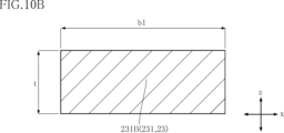
- the first suspension lead 23 has a first inner part 231 and a first outer part 232.
- the first inner part 231 is connected to the first die pad 21 and is covered by the sealing resin 50.
- the first outer part 232 is connected to the first inner part 231 and is exposed to the outside.
- the first outer part 232 extends in the second direction y.
- the first outer part 232 is bent in a gull-wing shape.
- the surface of the first outer part 232 is, for example, tin-plated.
- the first die pad 21 has a first edge 21B that extends in the first direction x and is located closest to the second side surface 54 of the sealing resin 50.
- the first inner portion 231 includes a first portion 231A that extends from the boundary with the extension line EL of the first edge 21B to the first die pad 21.
- the first portion 231A is spaced from the second side surface 54.
- the portion corresponding to the first portion 231A is indicated by hatching.
- the cross-sectional area of the first portion 231A in the direction in which it extends is larger than any cross-sectional area of the first outer portion 232 in the direction in which it extends.
- the "cross-sectional area in the direction in which it extends" refers to the area of a cross section perpendicular to the direction in which it extends.
- the first inner part 231 includes a second part 231B that connects the first part 231A and the first outer part 232.
- the portion corresponding to the second part 231B is shown hatched.
- the cross-sectional area of the second part 231B in the direction in which it extends is larger than any cross-sectional area of the first outer part 232 in the direction in which it extends.
- the second suspension lead 24 is located on the opposite side of the first die pad 21 from the first suspension lead 23 and is connected to the first die pad 21.
- the second suspension lead 24 is separated from the two first side surfaces 53 of the sealing resin 50.
- the second suspension lead 24 is exposed to the outside from the second side surface 54 of the sealing resin 50.
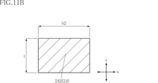
- the second suspension lead 24 has a second inner part 241 and a second outer part 242.
- the second inner part 241 is connected to the first die pad 21 and is covered by the sealing resin 50.
- the second outer part 242 is connected to the second inner part 241 and is exposed to the outside. When viewed in the third direction z, the second outer part 242 extends in the second direction y.
- the second outer part 242 is bent in a gull-wing shape when viewed in the first direction x.
- the surface of the second outer part 242 is, for example, tin-plated.
- Figures 11A and 11B similar to the case of the first suspension lead 23, the cross-sectional area of the second inner part 241 in the direction in which it extends is larger than any cross-sectional area of the second outer part 242 in the direction in which it extends.
- the first inner portion 231 of the first hanging lead 23 and the second inner portion 241 of the second hanging lead 24 each overlap the first die pad 21.
- the first inner portion 231, the second inner portion 241, and each of the multiple second holes 212 of the first die pad 21 each overlap an imaginary line VL extending along the first direction x.
- the second die pad 22 has a second mounting surface 22A that faces the same side as the first mounting surface 21A of the first die pad 21 in the third direction z.
- the second semiconductor element 12 is bonded to the second mounting surface 22A via a bonding layer 29.
- the second die pad 22 is covered with a sealing resin 50.
- the third suspension lead 25 is located on the side where the first suspension lead 23 is located with respect to the first die pad 21 as a reference, and is connected to the second die pad 22.
- the third suspension lead 25 is away from the two first side surfaces 53 of the sealing resin 50.
- the third suspension lead 25 is exposed to the outside from the third side surface 55 of the sealing resin 50.
- the third suspension lead 25 has a third inner part 251 and a third outer part 252.
- the third inner part 251 is connected to the second die pad 22 and is covered by the sealing resin 50.
- the third outer part 252 is connected to the third inner part 251 and is exposed to the outside. When viewed in the third direction z, the third outer part 252 extends in the second direction y.
- the third outer part 252 When viewed in the first direction x, the third outer part 252 is bent in a gull-wing shape.
- the surface of the third outer part 252 is, for example, tin-plated.
- the cross-sectional area of the third inner part 251 in the direction in which it extends is greater than any cross-sectional area of the third outer part 252 in the direction in which it extends.
- the fourth suspension lead 26 is located on the opposite side of the third suspension lead 25 with respect to the second die pad 22, and is connected to the second die pad 22.
- the fourth suspension lead 26 is separated from the two first side surfaces 53 of the sealing resin 50.
- the fourth suspension lead 26 is exposed to the outside from the third side surface 55 of the sealing resin 50.
- the fourth suspension lead 26 has a fourth inner part 261 and a fourth outer part 262.
- the fourth inner part 261 is connected to the second die pad 22 and is covered by the sealing resin 50.
- the fourth outer part 262 is connected to the fourth inner part 261 and is exposed to the outside. When viewed in the third direction z, the fourth outer part 262 extends in the second direction y.
- the fourth outer part 262 When viewed in the first direction x, the fourth outer part 262 is bent in a gull-wing shape.
- the surface of the fourth outer part 262 is, for example, tin-plated.
- the cross-sectional area of the fourth inner part 261 in the direction in which it extends is greater than any cross-sectional area of the fourth outer part 262 in the direction in which it extends.
- the two side leads 27 sandwich the third suspension lead 25 and the fourth suspension lead 26 in the first direction x.
- Each of the two side leads 27 is separated from the second die pad 22 and the two first side surfaces 53 of the sealing resin 50.
- Each of the two side leads 27 is exposed to the outside from the third side surface 55 of the sealing resin 50.
- Each of the two side leads 27 is electrically connected to the second semiconductor element 12 via one of the multiple fourth wires 44.
- each of the two side leads 27 has an inner portion 271 and an outer portion 272.
- the inner portion 271 is covered with sealing resin 50.
- the outer portion 272 is connected to the inner portion 271 and is exposed to the outside. When viewed in the third direction z, the outer portion 272 extends in the second direction y. As shown in FIG. 3, the outer portion 272 is bent in a gull-wing shape when viewed in the first direction x.
- the surface of the outer portion 272 is, for example, tin-plated.
- the third inner portion 251 of the third hanging lead 25, the fourth inner portion 261 of the fourth hanging lead 26, and the inner portions 271 of the two side leads 27 overlap the second die pad 22.
- the multiple first intermediate leads 31 are located between the first suspension lead 23 and the second suspension lead 24 in the first direction x.
- the multiple first intermediate leads 31 are located on the opposite side of the second die pad 22 with respect to the first die pad 21 in the second direction y.
- the multiple first intermediate leads 31 are arranged along the first direction x. At least one of the multiple first intermediate leads 31 is electrically connected to the first semiconductor element 11 via one of the multiple second wires 42.
- each of the multiple first intermediate leads 31 has an inner portion 311 and an outer portion 312.
- the inner portion 311 is covered with sealing resin 50.
- the outer portion 312 is connected to the inner portion 311 and is exposed to the outside from the second side surface 54 of the sealing resin 50.
- the outer portion 312 extends in the second direction y.
- the outer portion 312 is bent in a gull-wing shape.
- the shape of the outer portion 312 is equal to the shape of the second outer portion 242 of the second suspension lead 24 shown in FIG. 3.
- the surface of the outer portion 312 is, for example, tin-plated.
- the multiple second intermediate leads 32 are located between the third suspension lead 25 and the fourth suspension lead 26 in the first direction x.
- the multiple second intermediate leads 32 are located on the opposite side of the first die pad 21 with respect to the second die pad 22 in the second direction y.
- the multiple second intermediate leads 32 are arranged along the first direction x. At least one of the multiple second intermediate leads 32 is electrically connected to the second semiconductor element 12 via one of the multiple fourth wires 44.
- each of the second intermediate leads 32 has an inner portion 321 and an outer portion 322.
- the inner portion 321 is covered with the sealing resin 50.
- the outer portion 322 is connected to the inner portion 321 and is exposed to the outside from the third side surface 55 of the sealing resin 50.
- the outer portion 322 extends in the second direction y.
- the outer portion 322 is bent in a gull-wing shape.
- the shape of the outer portion 322 is equal to the shape of the outer portion 272 of one of the two side leads 27 shown in FIG. 3.
- the surface of the outer portion 322 is, for example, tin-plated.
- each of the multiple first wires 41 is conductively joined to one of the multiple third electrodes 131 of the insulating element 13 and one of the multiple first electrodes 111 of the first semiconductor element 11. This allows the first semiconductor element 11 to be electrically connected to the insulating element 13.
- the multiple first wires 41 are arranged along the first direction x. Any of the multiple first wires 41 straddles any of the multiple second holes 212 provided in the first die pad 21.
- the multiple first wires 41 contain, for example, gold.
- each of the multiple second wires 42 is conductively joined to one of the multiple first electrodes 111 of the first semiconductor element 11 and the inner portion 311 of one of the multiple first intermediate leads 31.
- at least one of the multiple first intermediate leads 31 is conductively connected to the first semiconductor element 11.
- At least one of the multiple second wires 42 is conductively joined to one of the multiple first electrodes 111 and the first inner portion 231 of the first suspension lead 23.
- the first suspension lead 23 is conductively connected to the first semiconductor element 11.
- at least one of the multiple second wires 42 is conductively joined to one of the multiple first electrodes 111 and the second inner portion 241 of the second suspension lead 24.
- the second suspension lead 24 is conductively connected to the first semiconductor element 11. At least one of the first suspension lead 23 and the second suspension lead 24 forms the ground of the first semiconductor element 11.
- the second wires 42 may include, for example, gold.
- each of the second wires 42 may include a core material including copper and a coating material including palladium that covers the core material.
- each of the multiple third wires 43 is conductively joined to one of the multiple fourth electrodes 132 of the insulating element 13 and one of the multiple second electrodes 121 of the second semiconductor element 12. This allows the second semiconductor element 12 to be electrically connected to the insulating element 13.
- the multiple third wires 43 are arranged along the first direction x.
- the multiple third wires 43 straddle the first die pad 21 and the second die pad 22.
- the multiple third wires 43 contain, for example, gold.
- each of the multiple fourth wires 44 is conductively joined to one of the multiple second electrodes 121 of the second semiconductor element 12 and the inner portion 321 of one of the multiple second intermediate leads 32.
- at least one of the multiple second intermediate leads 32 is conductively connected to the second semiconductor element 12.
- At least one of the multiple fourth wires 44 is conductively joined to one of the multiple second electrodes 121 and the third inner portion 251 of the third suspension lead 25.
- the third suspension lead 25 is conductively connected to the second semiconductor element 12.
- At least one of the multiple fourth wires 44 is conductively joined to one of the multiple second electrodes 121 and the fourth inner portion 261 of the fourth suspension lead 26.
- the fourth suspension lead 26 is conductively connected to the second semiconductor element 12. At least one of the third suspension lead 25 and the fourth suspension lead 26 forms the ground of the second semiconductor element 12. Furthermore, at least one of the multiple fourth wires 44 is conductively joined to one of the multiple second electrodes 121 and to the inner portion 271 of one of the two side leads 27. As a result, at least one of the two side leads 27 is electrically connected to the second semiconductor element 12.
- the multiple fourth wires 44 include, for example, gold.
- each of the multiple fourth wires 44 may include a core material including copper and a coating material including palladium that covers the core material.
- a half-bridge circuit including a low-side (low potential side) switching element and a high-side (high potential side) switching element is generally configured.
- these switching elements are MOSFETs.
- the reference potential of the source of the switching element and the gate driver that drives the switching element are both ground.
- the reference potential of the source of the switching element and the gate driver that drives the switching element are both equivalent to the potential at the output node of the half-bridge circuit.
- the reference potential of the gate driver that drives the high-side switching element changes.
- the reference potential is equivalent to the voltage applied to the drain of the high-side switching element (for example, 600V or more).
- the ground of the first semiconductor element 11 and the ground of the second semiconductor element 12 are configured to be separated. Therefore, when the semiconductor device A10 is used as a gate driver for driving a high-side switching element, a voltage equivalent to the voltage applied to the drain of the high-side switching element is transiently applied to the ground of the second semiconductor element 12.
- the semiconductor device A10 includes a first die pad 21, a first suspension lead 23, a second suspension lead 24, a first semiconductor element 11, and a sealing resin 50.
- the first suspension lead 23 has a first inner part 231 covered with the sealing resin 50, and a first outer part 232 connected to the first inner part 231 and exposed to the outside.
- the first inner part 231 includes a first part 231A extending from the boundary with the extension line EL of the first edge 21B of the first die pad 21 to the first die pad 21.
- the cross-sectional area of the first part 231A in the direction in which it extends is larger than any cross-sectional area of the first outer part 232 in the direction in which it extends.
- the bending rigidity of the cross section perpendicular to the direction in which the first inner part 231 extends is larger than the bending rigidity of the cross section perpendicular to the direction in which the first outer part 232 extends.
- the first inner part 231 of the first suspension lead 23 includes a second part 231B that connects the first part 231A and the first outer part 232.
- the cross-sectional area of the second part 231B in the direction in which it extends is greater than any cross-sectional area of the first outer part 232 in the direction in which it extends.
- the second suspension lead 24 has a second inner part 241 covered with sealing resin 50, and a second outer part 242 connected to the second inner part 241 and exposed to the outside.
- the cross-sectional area of the second inner part 241 in the direction in which it extends is larger than any cross-sectional area of the second outer part 242 in the direction in which it extends.
- the bending rigidity of the cross section perpendicular to the direction in which the second inner part 241 extends is larger than the bending rigidity of the cross section perpendicular to the direction in which the second outer part 242 extends.
- the semiconductor device A10 further includes an insulating element 13 mounted on the first die pad 21.
- the first die pad 21 is provided with two first holes 211 and a second hole 212, each of which penetrates in the third direction z.
- the two first holes 211 are located on both sides of the first semiconductor element 11 in the first direction x.
- the second hole 212 is located between the first semiconductor element 11 and the insulating element 13 in the second direction y.
- the first inner portion 231 of the first suspension lead 23, the second inner portion 241 of the second suspension lead 24, and the second hole 212 of the first die pad 21 each overlap the imaginary line VL extending along the first direction x.
- This configuration suppresses rotation of the first die pad 21 around the first direction x, which occurs when the fluidized sealing resin 50 comes into contact with the first die pad 21 when forming the sealing resin 50 in the manufacture of the semiconductor device A10.
- the second hole 212 take a shape that extends in the first direction x, rotation of the first die pad 21 around the first direction x can be more effectively suppressed.
- the first inner portion 231 of the first suspension lead 23 and the second inner portion 241 of the second suspension lead 24 each overlap the first die pad 21. This configuration makes it possible to suppress the expansion of the dimension of the semiconductor device A10 in the third direction z.
- FIG. 14 is seen through the sealing resin 50.
- the outline of the sealing resin 50 is shown by imaginary lines.
- the configurations of the first suspension lead 23, the second suspension lead 24, the third suspension lead 25, and the fourth suspension lead 26 are different from those of semiconductor device A10.
- a cut mark 232A facing the first direction x is formed on the first outer part 232 of the first suspension lead 23.
- the cut mark 232A is a trace formed on the first outer part 232 by cutting the two tie bars 82 shown in FIG. 17.
- the first suspension lead 23 is obtained from a lead frame 80 together with the first die pad 21 and the second die pad 22.
- the lead frame 80 has a frame portion 81 and two tie bars 82.
- the frame portion 81 surrounds the first die pad 21 and the second die pad 22.
- the first die pad 21, the second die pad 22, the first suspension lead 23, the second suspension lead 24, the third suspension lead 25, the fourth suspension lead 26, the two side leads 27, the multiple first intermediate leads 31, and the multiple second intermediate leads 32 are connected to the frame portion 81.
- the two tie bars 82 are spaced apart from each other in the second direction y. Each of the two tie bars 82 is connected to the frame portion 81 on both sides in the first direction x.
- the first suspension lead 23, the second suspension lead 24, and the multiple first intermediate leads 31 are each connected to one of the two tie bars 82.
- the third suspension lead 25, the fourth suspension lead 26, the two side leads 27, and the multiple second intermediate leads 32 are each connected to the other of the two tie bars 82.
- the two tie bars 82 are cut.
- a cut mark 232A is formed in the first outer part 232, and the first outer part 232 is formed into a gull-wing shape.
- the first outer portion 232 of the first suspension lead 23 includes a third portion 232B and a fourth portion 232C.
- the third portion 232B is located between the second side surface 54 of the sealing resin 50 and the cut mark 232A.
- the fourth portion 232C is located on the opposite side of the cut mark 232A from the third portion 232B.
- the portions corresponding to the third portion 232B and the fourth portion 232C are shown by hatching.
- the cross-sectional area of the third portion 232B in the direction in which it extends is larger than the cross-sectional area of the fourth portion 232C in the direction in which it extends.
- the cross-sectional area of the first portion 231A of the first inner portion 231 of the first suspension lead 23 in the direction in which it extends is also larger than any cross-sectional area of the first outer portion 232 in the direction in which it extends.
- the cross-sectional area of the third portion 232B of the first outer portion 232 of the first suspension lead 23 in the direction in which it extends is equal to the cross-sectional area of the second portion 231B of the first inner portion 231 in the direction in which it extends.
- the second outer part 242 of the second hanging lead 24, the third outer part 252 of the third hanging lead 25, and the fourth outer part 262 of the fourth hanging lead 26 each have a configuration similar to the cut mark 232A, the third part 232B, and the fourth part 232C of the first outer part 232 of the first hanging lead 23.
- the semiconductor device A20 includes a first die pad 21, a first suspension lead 23, a second suspension lead 24, a first semiconductor element 11, and sealing resin 50.
- the first suspension lead 23 has a first inner part 231 covered with sealing resin 50, and a first outer part 232 connected to the first inner part 231 and exposed to the outside.
- the first inner part 231 includes a first part 231A extending from the boundary with the extension line EL of the first edge 21B of the first die pad 21 to the first die pad 21.
- the cross-sectional area of the first part 231A in the direction in which it extends is larger than any cross-sectional area of the first outer part 232 in the direction in which it extends.
- the semiconductor device A20 it is possible to stabilize the posture of the die pad during the manufacture of the semiconductor device A20. Furthermore, the semiconductor device A20 has a configuration in common with the semiconductor device A10, and thus achieves the same effects as the semiconductor device A10.
- the first outer part 232 of the first suspension lead 23 includes a third part 232B and a fourth part 232C.
- the third part 232B is located between the second side surface 54 of the sealing resin 50 and the cut mark 232A.
- the fourth part 232C is located on the opposite side of the cut mark 232A to the third part 232B.
- the cross-sectional area of the third part 232B in the direction in which it extends is larger than the cross-sectional area of the fourth part 232C in the direction in which it extends.
- FIG. 21 shows the sealing resin 50 through the view.
- the outline of the sealing resin 50 is shown by imaginary lines.
- the semiconductor device A30 differs from the semiconductor device A10 in that it has two support leads 28 instead of two side leads 27. Furthermore, the number of the first intermediate leads 31 and the number of the second intermediate leads 32 are smaller in the semiconductor device A30 than in the semiconductor device A10.
- the two support leads 28 are spaced apart from each other in the second direction y. Each of the two support leads 28 extends in the second direction y. The two support leads 28 are individually connected to the first die pad 21 and the second die pad 22. As shown in FIGS. 22 and 23, each of the two support leads 28 has an end face 28A facing the second direction y. The end face 28A of the support lead 28 connected to the first die pad 21 is exposed from the second side surface 54 of the sealing resin 50. The end face 28A of the support lead 28 connected to the second die pad 22 is exposed from the third side surface 55 of the sealing resin 50.
- the cross-sectional area of the first part 231A of the first inner part 231 of the first suspension lead 23 in the direction in which it extends is larger than any cross-sectional area of the first outer part 232 in the direction in which it extends.
- the cross-sectional area of the second part 231B of the first inner part 231 of the first suspension lead 23 in the direction in which it extends is larger than any cross-sectional area of the first outer part 232 in the direction in which it extends.
- the semiconductor device A30 includes a first die pad 21, a first suspension lead 23, a second suspension lead 24, a first semiconductor element 11, and sealing resin 50.
- the first suspension lead 23 has a first inner part 231 covered with sealing resin 50, and a first outer part 232 connected to the first inner part 231 and exposed to the outside.
- the first inner part 231 includes a first part 231A extending from the boundary with the extension line EL of the first edge 21B of the first die pad 21 to the first die pad 21.
- the cross-sectional area of the first part 231A in the direction in which it extends is larger than any cross-sectional area of the first outer part 232 in the direction in which it extends.
- the semiconductor device A30 it is possible to stabilize the posture of the die pad during the manufacture of the semiconductor device A30. Furthermore, the semiconductor device A30 has a configuration in common with the semiconductor device A10, and thus achieves the same effects as the semiconductor device A10.
- the semiconductor device A30 further includes a support lead 28.
- the support lead 28 is connected to the first die pad 21 and is exposed to the outside from the second side surface 54 of the sealing resin 50. With this configuration, when a load in the third direction z acts on the first die pad 21, the support lead 28 resists bending in the third direction z together with the first suspension lead 23. This further reduces the deflection of the first suspension lead 23 in the third direction z compared to the case of the semiconductor device A10, thereby further stabilizing the posture of the first die pad 21.
- a first die pad A first die pad; a first suspension lead connected to one side of the first die pad in a first direction; a second suspension lead located on an opposite side of the first die pad from the first suspension lead and connected to the first die pad; a first semiconductor element mounted on the first die pad; a sealing resin that covers the first die pad and the first semiconductor element, the sealing resin has two first side surfaces facing opposite sides to each other in the first direction and a second side surface facing a second direction perpendicular to the first direction; each of the first suspension lead and the second suspension lead is spaced apart from the two first side faces and exposed to the outside from the second side face; the first suspension lead has a first inner portion covered with the sealing resin and a first outer portion connected to the first inner portion and exposed to the outside, the first die pad has a first edge extending in the first direction and located closest to the second side; When viewed in a third direction perpendicular to the first direction and the second direction, the first inner portion includes a first
- the first inner portion includes a second portion that connects the first portion and the first outer portion, 2.
- the second suspension lead has a second inner portion covered with the sealing resin and a second outer portion connected to the second inner portion and exposed to the outside, 3.
- the semiconductor device according to claim 2 wherein a cross-sectional area of the second inner portion in the direction in which the second inner portion extends is larger than any cross-sectional area of the second outer portion in the direction in which the second inner portion extends.
- each of the first outer part and the second outer part extends in the second direction.
- Appendix 5 A cut mark facing the first direction is formed in the first outer portion, the first outer portion includes a third portion located between the second side surface and the cut mark, and a fourth portion located on an opposite side of the cut mark from the third portion, 5.
- the semiconductor device according to claim 4 wherein a cross-sectional area of the third portion in the direction in which it extends is larger than a cross-sectional area of the fourth portion in the direction in which it extends.
- Appendix 6. a second die pad spaced apart from the first die pad in the second direction; a second semiconductor element mounted on the second die pad; 6.
- the third suspension lead has a third inner portion covered with the sealing resin and a third outer portion connected to the third inner portion and exposed to the outside, 8.
- a cross-sectional area of the third inner portion in the direction in which it extends is larger than any cross-sectional area of the third outer portion in the direction in which it extends.
- Appendix 9. The semiconductor device according to claim 8, wherein an area of the first die pad is larger than an area of the second die pad when viewed in the third direction.
- the insulating element is located adjacent to the first semiconductor element in the second direction; the first die pad is provided with two first holes and a second hole each penetrating the first die pad in the third direction; the two first holes are located on both sides of the first semiconductor element in the first direction, 11.
- the semiconductor device according to claim 10 wherein the second hole is located between the first semiconductor element and the insulating element in the second direction.
- Appendix 12. The semiconductor device according to claim 11, wherein the second hole extends in the first direction.
- Appendix 13 13.
- each of the first inner portion and the second inner portion overlaps the first die pad.
- Appendix 15. The semiconductor device according to claim 14, wherein, when viewed in the first direction, the third inner portion overlaps the second die pad.
- Appendix 16. further comprising a plurality of first intermediate leads located between the first suspension lead and the second suspension lead; 16. The semiconductor device according to claim 15, wherein at least one of the plurality of first intermediate leads is electrically connected to the first semiconductor element.
- Appendix 17. further comprising a plurality of second intermediate leads located between the third suspension lead and the fourth suspension lead; 17. The semiconductor device according to claim 16, wherein at least one of the plurality of second intermediate leads is electrically connected to the second semiconductor element.
Landscapes
- Lead Frames For Integrated Circuits (AREA)
- Engineering & Computer Science (AREA)
- Microelectronics & Electronic Packaging (AREA)
- Structures Or Materials For Encapsulating Or Coating Semiconductor Devices Or Solid State Devices (AREA)
Priority Applications (4)
| Application Number | Priority Date | Filing Date | Title |
|---|---|---|---|
| JP2024565775A JPWO2024135356A1 (https=) | 2022-12-21 | 2023-12-06 | |
| DE112023005272.7T DE112023005272T5 (de) | 2022-12-21 | 2023-12-06 | Halbleiterbauelement |
| CN202380086305.6A CN120476473A (zh) | 2022-12-21 | 2023-12-06 | 半导体装置 |
| US19/237,837 US20250309068A1 (en) | 2022-12-21 | 2025-06-13 | Semiconductor device |
Applications Claiming Priority (2)
| Application Number | Priority Date | Filing Date | Title |
|---|---|---|---|
| JP2022204281 | 2022-12-21 | ||
| JP2022-204281 | 2022-12-21 |
Related Child Applications (1)
| Application Number | Title | Priority Date | Filing Date |
|---|---|---|---|
| US19/237,837 Continuation US20250309068A1 (en) | 2022-12-21 | 2025-06-13 | Semiconductor device |
Publications (1)
| Publication Number | Publication Date |
|---|---|
| WO2024135356A1 true WO2024135356A1 (ja) | 2024-06-27 |
Family
ID=91588346
Family Applications (1)
| Application Number | Title | Priority Date | Filing Date |
|---|---|---|---|
| PCT/JP2023/043583 Ceased WO2024135356A1 (ja) | 2022-12-21 | 2023-12-06 | 半導体装置 |
Country Status (5)
| Country | Link |
|---|---|
| US (1) | US20250309068A1 (https=) |
| JP (1) | JPWO2024135356A1 (https=) |
| CN (1) | CN120476473A (https=) |
| DE (1) | DE112023005272T5 (https=) |
| WO (1) | WO2024135356A1 (https=) |
Citations (3)
| Publication number | Priority date | Publication date | Assignee | Title |
|---|---|---|---|---|
| JPH10144855A (ja) * | 1996-11-13 | 1998-05-29 | Mitsubishi Electric Corp | リードフレームとこれを用いた半導体装置 |
| US8441325B2 (en) * | 2004-06-03 | 2013-05-14 | Silicon Laboratories Inc. | Isolator with complementary configurable memory |
| JP2016207714A (ja) * | 2015-04-16 | 2016-12-08 | ローム株式会社 | 半導体装置 |
-
2023
- 2023-12-06 WO PCT/JP2023/043583 patent/WO2024135356A1/ja not_active Ceased
- 2023-12-06 CN CN202380086305.6A patent/CN120476473A/zh active Pending
- 2023-12-06 JP JP2024565775A patent/JPWO2024135356A1/ja active Pending
- 2023-12-06 DE DE112023005272.7T patent/DE112023005272T5/de active Pending
-
2025
- 2025-06-13 US US19/237,837 patent/US20250309068A1/en active Pending
Patent Citations (3)
| Publication number | Priority date | Publication date | Assignee | Title |
|---|---|---|---|---|
| JPH10144855A (ja) * | 1996-11-13 | 1998-05-29 | Mitsubishi Electric Corp | リードフレームとこれを用いた半導体装置 |
| US8441325B2 (en) * | 2004-06-03 | 2013-05-14 | Silicon Laboratories Inc. | Isolator with complementary configurable memory |
| JP2016207714A (ja) * | 2015-04-16 | 2016-12-08 | ローム株式会社 | 半導体装置 |
Also Published As
| Publication number | Publication date |
|---|---|
| DE112023005272T5 (de) | 2025-12-11 |
| US20250309068A1 (en) | 2025-10-02 |
| CN120476473A (zh) | 2025-08-12 |
| JPWO2024135356A1 (https=) | 2024-06-27 |
Similar Documents
| Publication | Publication Date | Title |
|---|---|---|
| US7615854B2 (en) | Semiconductor package that includes stacked semiconductor die | |
| JP7527916B2 (ja) | 半導体装置 | |
| WO2022202129A1 (ja) | 半導体装置 | |
| WO2023140042A1 (ja) | 半導体装置 | |
| JP2021082794A (ja) | 電子部品および電子装置 | |
| US20240047438A1 (en) | Semiconductor equipment | |
| US12616040B2 (en) | Metal layer plated to inner leads of a leadframe | |
| US20240312877A1 (en) | Semiconductor device | |
| JP7843276B2 (ja) | 半導体装置 | |
| WO2024135356A1 (ja) | 半導体装置 | |
| JP7791168B2 (ja) | 半導体装置 | |
| US20240030109A1 (en) | Semiconductor device | |
| US20260018562A1 (en) | Semiconductor device | |
| JP7837876B2 (ja) | 半導体装置 | |
| US20250006775A1 (en) | Semiconductor element and semiconductor device | |
| US20250070076A1 (en) | Semiconductor device | |
| US20260096448A1 (en) | Semiconductor device | |
| JP7694167B2 (ja) | 半導体装置 | |
| WO2024257543A1 (ja) | 半導体装置 | |
| WO2024195480A1 (ja) | 半導体装置 | |
| WO2025069992A1 (ja) | 半導体装置 | |
| WO2023199808A1 (ja) | 半導体装置 |
Legal Events
| Date | Code | Title | Description |
|---|---|---|---|
| 121 | Ep: the epo has been informed by wipo that ep was designated in this application |
Ref document number: 23906722 Country of ref document: EP Kind code of ref document: A1 |
|
| WWE | Wipo information: entry into national phase |
Ref document number: 2024565775 Country of ref document: JP |
|
| WWE | Wipo information: entry into national phase |
Ref document number: 202380086305.6 Country of ref document: CN |
|
| WWE | Wipo information: entry into national phase |
Ref document number: 112023005272 Country of ref document: DE |
|
| WWP | Wipo information: published in national office |
Ref document number: 202380086305.6 Country of ref document: CN |
|
| WWP | Wipo information: published in national office |
Ref document number: 112023005272 Country of ref document: DE |
|
| 122 | Ep: pct application non-entry in european phase |
Ref document number: 23906722 Country of ref document: EP Kind code of ref document: A1 |