WO2024134780A1 - 露光システム、及び電子デバイスの製造方法 - Google Patents
露光システム、及び電子デバイスの製造方法 Download PDFInfo
- Publication number
- WO2024134780A1 WO2024134780A1 PCT/JP2022/046927 JP2022046927W WO2024134780A1 WO 2024134780 A1 WO2024134780 A1 WO 2024134780A1 JP 2022046927 W JP2022046927 W JP 2022046927W WO 2024134780 A1 WO2024134780 A1 WO 2024134780A1
- Authority
- WO
- WIPO (PCT)
- Prior art keywords
- exposure system
- pupil
- optical system
- photosensitive substrate
- exposure
- Prior art date
- Legal status (The legal status is an assumption and is not a legal conclusion. Google has not performed a legal analysis and makes no representation as to the accuracy of the status listed.)
- Ceased
Links
Images











Classifications
-
- G—PHYSICS
- G03—PHOTOGRAPHY; CINEMATOGRAPHY; ANALOGOUS TECHNIQUES USING WAVES OTHER THAN OPTICAL WAVES; ELECTROGRAPHY; HOLOGRAPHY
- G03F—PHOTOMECHANICAL PRODUCTION OF TEXTURED OR PATTERNED SURFACES, e.g. FOR PRINTING, FOR PROCESSING OF SEMICONDUCTOR DEVICES; MATERIALS THEREFOR; ORIGINALS THEREFOR; APPARATUS SPECIALLY ADAPTED THEREFOR
- G03F7/00—Photomechanical, e.g. photolithographic, production of textured or patterned surfaces, e.g. printing surfaces; Materials therefor, e.g. comprising photoresists; Apparatus specially adapted therefor
- G03F7/20—Exposure; Apparatus therefor
- G03F7/2002—Exposure; Apparatus therefor with visible light or UV light, through an original having an opaque pattern on a transparent support, e.g. film printing, projection printing; by reflection of visible or UV light from an original such as a printed image
- G03F7/2008—Exposure; Apparatus therefor with visible light or UV light, through an original having an opaque pattern on a transparent support, e.g. film printing, projection printing; by reflection of visible or UV light from an original such as a printed image characterised by the reflectors, diffusers, light or heat filtering means or anti-reflective means used
-
- G—PHYSICS
- G03—PHOTOGRAPHY; CINEMATOGRAPHY; ANALOGOUS TECHNIQUES USING WAVES OTHER THAN OPTICAL WAVES; ELECTROGRAPHY; HOLOGRAPHY
- G03F—PHOTOMECHANICAL PRODUCTION OF TEXTURED OR PATTERNED SURFACES, e.g. FOR PRINTING, FOR PROCESSING OF SEMICONDUCTOR DEVICES; MATERIALS THEREFOR; ORIGINALS THEREFOR; APPARATUS SPECIALLY ADAPTED THEREFOR
- G03F7/00—Photomechanical, e.g. photolithographic, production of textured or patterned surfaces, e.g. printing surfaces; Materials therefor, e.g. comprising photoresists; Apparatus specially adapted therefor
- G03F7/20—Exposure; Apparatus therefor
-
- G—PHYSICS
- G03—PHOTOGRAPHY; CINEMATOGRAPHY; ANALOGOUS TECHNIQUES USING WAVES OTHER THAN OPTICAL WAVES; ELECTROGRAPHY; HOLOGRAPHY
- G03F—PHOTOMECHANICAL PRODUCTION OF TEXTURED OR PATTERNED SURFACES, e.g. FOR PRINTING, FOR PROCESSING OF SEMICONDUCTOR DEVICES; MATERIALS THEREFOR; ORIGINALS THEREFOR; APPARATUS SPECIALLY ADAPTED THEREFOR
- G03F7/00—Photomechanical, e.g. photolithographic, production of textured or patterned surfaces, e.g. printing surfaces; Materials therefor, e.g. comprising photoresists; Apparatus specially adapted therefor
- G03F7/20—Exposure; Apparatus therefor
- G03F7/2002—Exposure; Apparatus therefor with visible light or UV light, through an original having an opaque pattern on a transparent support, e.g. film printing, projection printing; by reflection of visible or UV light from an original such as a printed image
- G03F7/2004—Exposure; Apparatus therefor with visible light or UV light, through an original having an opaque pattern on a transparent support, e.g. film printing, projection printing; by reflection of visible or UV light from an original such as a printed image characterised by the use of a particular light source, e.g. fluorescent lamps or deep UV light
- G03F7/2006—Exposure; Apparatus therefor with visible light or UV light, through an original having an opaque pattern on a transparent support, e.g. film printing, projection printing; by reflection of visible or UV light from an original such as a printed image characterised by the use of a particular light source, e.g. fluorescent lamps or deep UV light using coherent light; using polarised light
Definitions
- the present disclosure relates to an exposure system and a method for manufacturing an electronic device.
- gas laser devices used for exposure include KrF excimer laser devices that output laser light with a wavelength of approximately 248 nm, and ArF excimer laser devices that output laser light with a wavelength of approximately 193 nm.
- the spectral linewidth of the natural oscillation light of KrF excimer laser devices and ArF excimer laser devices is wide, at 350 to 400 pm. Therefore, if a projection lens is made of a material that transmits ultraviolet light, such as KrF and ArF laser light, chromatic aberration may occur. As a result, the resolution may decrease. Therefore, it is necessary to narrow the spectral linewidth of the laser light output from the gas laser device to a level where chromatic aberration can be ignored. For this reason, a line narrowing module (LNM) containing a narrowing element (such as an etalon or grating) may be installed inside the laser resonator of the gas laser device to narrow the spectral linewidth.
- LNM line narrowing module
- a gas laser device in which the spectral linewidth is narrowed is called a narrow-line laser device.
- an exposure system includes an illumination optical system that illuminates a photomask with pulsed laser light containing multiple central wavelengths, and a projection optical system that illuminates a photosensitive substrate with the pulsed laser light that has passed through the photomask to project an image of the photomask, and the position of a first pupil, which is the pupil of the illumination optical system, is shifted from a reference position that is conjugate with a second pupil, which is the pupil of the projection optical system, in a direction that reduces the deviation of the imaging position due to lateral chromatic aberration on the photosensitive substrate by magnification telecentric error.
- a method for manufacturing an electronic device includes exposing a photosensitive substrate to pulsed laser light in order to manufacture an electronic device, using an exposure system that includes an illumination optical system that illuminates a photomask with pulsed laser light having multiple central wavelengths, and a projection optical system that illuminates a photosensitive substrate with the pulsed laser light that has passed through the photomask to project an image of the photomask, and in which the position of a first pupil, which is the pupil of the illumination optical system, is shifted from a reference position that is conjugate with a second pupil, which is the pupil of the projection optical system, in a direction that reduces the shift in the imaging position due to lateral chromatic aberration on the photosensitive substrate by magnification telecentric error.
- FIG. 1 shows a schematic configuration of an exposure system in a comparative example.
- FIG. 2 shows a schematic configuration of the laser device.
- FIG. 3 is a graph showing a periodic change in wavelength.
- FIG. 4 shows an integrated spectrum of a pulsed laser beam containing a plurality of central wavelengths.
- FIG. 5 shows a photosensitive substrate being exposed by an exposure apparatus.
- FIG. 6 is a diagram for explaining how the position of the scan field on the photosensitive substrate changes with respect to the position of the beam cross section of the pulsed laser light.
- FIG. 7 is a diagram for explaining how the position of the scan field on the photosensitive substrate changes with respect to the position of the beam cross section of the pulsed laser light.
- FIG. 8 is a diagram for explaining how the position of the scan field on the photosensitive substrate changes with respect to the position of the beam cross section of the pulsed laser light.
- FIG. 9 is a schematic diagram of a projection optical system included in the exposure apparatus.
- FIG. 10 shows how the image formed on the photosensitive substrate by the projection optical system shown in FIG. 9 is deformed.
- FIG. 11 is a schematic diagram of an optical system including a part of an illumination optical system and a double-telecentric projection optical system.
- FIG. 12 shows a change in the chief ray when the pupil of the illumination optical system in the optical system shown in FIG. 11 is shifted in the direction of the optical axis.
- FIG. 13 is a diagram for explaining the state in which an image formed on a photosensitive substrate by the optical system shown in FIG.
- FIG. 14 is a diagram for explaining the state in which an image formed on a photosensitive substrate by the optical system shown in FIG. 12 changes.
- FIG. 15 is a diagram for explaining the state in which an image formed on a photosensitive substrate by the optical system shown in FIG. 12 changes.
- FIG. 16 shows a change in the chief ray when the pupil of the illumination optical system in the optical system shown in FIG. 11 is shifted in the opposite direction to that in FIG.
- FIG. 17 is a diagram for explaining the state in which an image formed on a photosensitive substrate by the optical system shown in FIG. 16 changes.
- FIG. 18 is a diagram for explaining the state in which an image formed on a photosensitive substrate by the optical system shown in FIG. 16 changes.
- FIG. 16 shows a change in the chief ray when the pupil of the illumination optical system in the optical system shown in FIG. 11 is shifted in the opposite direction to that in FIG.
- FIG. 17 is a diagram for explaining the state in which an image formed on a photosensitive substrate by the optical system shown in
- FIG. 19 is a diagram for explaining the state in which an image formed on a photosensitive substrate by the optical system shown in FIG. 16 changes.
- FIG. 20 is a schematic diagram showing a part of a marginal ray of a pulsed laser beam that is incident on the workpiece table when longitudinal chromatic aberration and transverse chromatic aberration are occurring.
- FIG. 21 shows a schematic diagram of an imaging area of light of each wavelength of the pulsed laser light shown in FIG.
- FIG. 22 is a cross-sectional view showing a resist profile when the photosensitive substrate exposed to the pulsed laser beam shown in FIGS. 20 and 21 is developed.
- FIG. 23 shows image shifts on a photosensitive substrate scan-exposed with the pulsed laser beam shown in FIGS.
- FIG. 20 is a schematic diagram showing a part of a marginal ray of a pulsed laser beam that is incident on the workpiece table when longitudinal chromatic aberration and transverse chromatic aberration are occurring.
- FIG. 21 shows a schematic diagram of an imaging area of
- FIG. 24 is a schematic diagram showing a part of the chief ray of the pulsed laser beam incident on the workpiece table when a magnification telecentric error occurs.
- FIG. 25 shows a schematic diagram of an imaging area of light of each wavelength of the pulsed laser light shown in FIG.
- FIG. 26 shows a schematic diagram of an image-forming area of light of each wavelength when transverse chromatic aberration is taken into consideration in the pulsed laser beam shown in FIG.
- FIG. 27 is a schematic diagram showing a part of the chief ray of the pulsed laser beam incident on the workpiece table when a magnification telecentric error occurs in the opposite direction to that in FIG. 24 .
- FIG. 28 shows a schematic diagram of an imaging area of light of each wavelength of the pulsed laser light shown in FIG. FIG.
- FIG. 29 shows a schematic diagram of an image-forming area of light of each wavelength when transverse chromatic aberration is taken into consideration in the pulsed laser beam shown in FIG.
- FIG. 30 shows a schematic configuration of an exposure system in the first embodiment.
- FIG. 31 conceptually illustrates a first example of an illumination optical system in which the pupil position is movable.
- FIG. 32 conceptually illustrates a second example of an illumination optical system in which the pupil position is movable.
- FIG. 33 conceptually illustrates a third example of an illumination optical system in which the pupil position is movable.
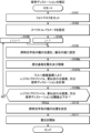
- FIG. 34 is a flowchart showing the process of correcting magnification distortion in the first embodiment.
- FIG. 35 shows a schematic configuration of an exposure system in the second embodiment.
- FIG. 36 is a flowchart showing a process for creating a correction table in the second embodiment.
- FIG. 37 shows an example of a correction table stored in the non-volatile memory.
- FIG. 38 is a flowchart showing a process for correcting magnification distortion in the second embodiment.
- FIG. 39 shows a schematic configuration of an exposure system in the third embodiment.
- FIG. 40 is a flowchart showing the process of correcting magnification distortion in the third embodiment.
- Exposure system that determines the position of the pupil IP of the illumination optical system 201 based on the spectral parameters 3.1 Configuration 3.2 Operation 3.2.1 Creation of a correction table 3.2.2 Correction of magnification distortion 3.3 Function 4. Exposure system including the measurement unit 303b separate from the exposure apparatus 200 4.1 Configuration 4.2 Operation (correction of magnification distortion) 4.3 Function 5. Other
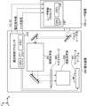
- FIG. 1 shows a schematic configuration of an exposure system in a comparative example.
- the comparative example of the present disclosure is a form that the applicant recognizes as being known only by the applicant, and is not a publicly known example that the applicant acknowledges.
- FIG. 1 shows an X-axis, a Y-axis, and a Z-axis that are perpendicular to each other.
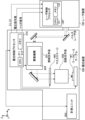
- the exposure system includes a laser device 100 and an exposure device 200. In FIG. 1, the laser device 100 is shown in a simplified form.
- the laser device 100 includes a laser control processor 130.
- the laser control processor 130 is a processing device including a memory 132 in which a control program is stored, and a CPU (central processing unit) 131 that executes the control program.
- the laser control processor 130 is specially configured or programmed to execute the various processes included in this disclosure.
- the laser device 100 is configured to output pulsed laser light toward the exposure device 200.
- the exposure apparatus 200 includes an illumination optical system 201, a projection optical system 202, and an exposure control processor 210.
- the illumination optical system 201 illuminates a pulsed laser beam incident from the laser apparatus 100 onto a photomask (not shown) arranged on a mask stage MS.
- the projection optical system 202 illuminates the pulsed laser light that has passed through the photomask onto a workpiece (not shown) placed on the workpiece table WT, projecting an image of the photomask.
- the workpiece is a photosensitive substrate such as a semiconductor wafer coated with a resist film.
- the exposure control processor 210 is a processing device including a memory 212 in which a control program is stored, and a CPU 211 that executes the control program.
- the exposure control processor 210 corresponds to the processor in this disclosure.
- the exposure control processor 210 is specially configured or programmed to execute the various processes included in this disclosure.
- the exposure control processor 210 manages the control of the exposure device 200, and transmits and receives various parameters and various signals to and from the laser control processor 130.
- the exposure control processor 210 transmits various parameters including the target short wavelength ⁇ 1, the target long wavelength ⁇ 2, and a voltage command value, and a trigger signal to the laser control processor 130.
- the laser control processor 130 controls the laser device 100 according to these parameters and signals.
- the target short wavelength ⁇ 1 corresponds to the first wavelength in this disclosure
- the target long wavelength ⁇ 2 corresponds to the second wavelength in this disclosure.
- the exposure control processor 210 synchronizes the mask stage MS and the workpiece table WT and translates them in opposite directions. This exposes the workpiece to pulsed laser light that reflects the mask pattern of the photomask.
- the mask pattern is transferred to a photosensitive substrate using photolithography in the manner described above. Electronic devices can then be manufactured through multiple steps.
- Fig. 2 shows a schematic configuration of the laser apparatus 100.
- an exposure apparatus 200 is shown in a simplified form.
- the laser apparatus 100 includes a laser control processor 130, a laser chamber 10, a pulse power module (PPM) 13, a line narrowing module 14, an output coupling mirror 15, and a monitor module 17.
- PPM pulse power module
- the line narrowing module 14 and the output coupling mirror 15 form an optical resonator.
- the laser chamber 10 is disposed in the optical path of the optical resonator.
- the laser chamber 10 is provided with windows 10a and 10b.
- the laser chamber 10 is internally provided with a discharge electrode 11a and a paired discharge electrode (not shown).
- the laser chamber 10 is filled with a laser gas that includes, for example, argon gas or krypton gas as a rare gas, fluorine gas as a halogen gas, and neon gas as a buffer gas.
- the pulse power module 13 includes a switch (not shown) and is connected to a charger (not shown).
- the line narrowing module 14 includes prisms 41 to 43, a grating 53, and a mirror 63. Details of the line narrowing module 14 will be described later.
- the output coupling mirror 15 is composed of a partial reflection mirror.
- a beam splitter 16 is disposed in the optical path of the pulsed laser light output from the output coupling mirror 15. The beam splitter 16 transmits part of the pulsed laser light with high transmittance and reflects the other part.
- a monitor module 17 is disposed in the optical path of the pulsed laser light reflected by the beam splitter 16.
- the laser control processor 130 acquires various parameters including the target short wavelength ⁇ 1, the target long wavelength ⁇ 2, and a voltage command value from the exposure control processor 210.
- the laser control processor 130 transmits a control signal to the line narrowing module 14 based on the target short wavelength ⁇ 1 and the target long wavelength ⁇ 2.
- the laser control processor 130 receives a trigger signal from the exposure control processor 210.
- the laser control processor 130 transmits an oscillation trigger signal based on the trigger signal to the pulse power module 13.
- the switch included in the pulse power module 13 turns on when it receives the oscillation trigger signal from the laser control processor 130.
- the pulse power module 13 generates a pulsed high voltage from the electrical energy stored in the charger and applies this high voltage to the discharge electrode 11a.
- Light generated within the laser chamber 10 is emitted to the outside of the laser chamber 10 through windows 10a and 10b.
- the light emitted from window 10a enters the line narrowing module 14.
- light close to the desired wavelength is folded back by the line narrowing module 14 and returned to the laser chamber 10.
- the output coupling mirror 15 transmits a portion of the light emitted from the window 10b and outputs it, and reflects the other portion back into the laser chamber 10.
- the light emitted from the laser chamber 10 travels back and forth between the line narrowing module 14 and the output coupling mirror 15.
- This light is amplified each time it passes through the discharge space in the laser chamber 10.
- this light is narrowed in line each time it is turned back by the line narrowing module 14, becoming light with a steep wavelength distribution with a central wavelength that is part of the range of wavelengths selected by the line narrowing module 14.
- the light that has been laser oscillated and narrowed in line in this way is output from the output coupling mirror 15 as pulsed laser light.
- the monitor module 17 measures the central wavelength of the pulsed laser light and transmits the measured wavelength to the laser control processor 130.
- the laser control processor 130 feedback controls the line narrowing module 14 based on the measured wavelength.
- the pulsed laser light that passes through the beam splitter 16 enters the exposure device 200.
- the prisms 41 to 43 are arranged in the optical path of the light beam emitted from the window 10a in ascending order of their numbers.
- the prism 43 can be rotated around an axis perpendicular to the paper surface of FIG. 2 by a rotation stage 143.
- Mirror 63 is disposed in the optical path of the light beam that has passed through prisms 41 to 43. Mirror 63 can be rotated around an axis perpendicular to the plane of FIG. 2 by rotation stage 163. Grating 53 is disposed in the optical path of the light beam reflected by mirror 63.
- the light beam emitted from the window 10a is expanded in beam width in a plane parallel to the paper surface of Fig. 2 by each of the prisms 41 to 43.
- the light beam transmitted through the prisms 41 to 43 is reflected by the mirror 63 and enters the grating 53.
- the light beam incident on the grating 53 is reflected by the multiple grooves of the grating 53 and diffracted in a direction according to the wavelength of the light.
- the grating 53 is arranged in a Littrow configuration so that the angle of incidence of the light beam incident on the grating 53 from the mirror 63 matches the diffraction angle of the diffracted light of the desired wavelength.
- the mirror 63 and prisms 41 to 43 reduce the beam width of the light beam returned from the grating 53 in a plane parallel to the paper surface of FIG. 2, and return the light beam to the inside of the laser chamber 10 through the window 10a.
- the laser control processor 130 controls the rotation stages 143 and 163 via a driver (not shown). Depending on the rotation angle of the rotation stages 143 and 163, the angle of incidence of the light beam incident on the grating 53 changes, and the wavelength selected by the line narrowing module 14 changes.
- the laser control processor 130 controls the rotation stage 163 so that the attitude of the mirror 63 changes periodically for every multiple pulses, based on the target short wavelength ⁇ 1 and the target long wavelength ⁇ 2 received from the exposure control processor 210.
- the central wavelength of the pulsed laser light changes periodically between the target short wavelength ⁇ 1 and the target long wavelength ⁇ 2 for every multiple pulses.
- the laser device 100 outputs a pulsed laser light containing multiple central wavelengths.
- the focal length in the exposure device 200 depends on the wavelength of the pulsed laser light.
- the pulsed laser light that is oscillated at multiple wavelengths and enters the exposure device 200 can be imaged at multiple different positions in the direction of the optical path axis of the pulsed laser light, so the focal depth can be effectively increased. For example, even when exposing a resist film with a large thickness, the imaging performance in the thickness direction of the resist film can be maintained.
- the resist profile which indicates the cross-sectional shape of the developed resist film, can be adjusted.
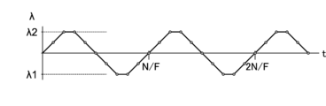
- Fig. 3 is a graph showing periodic wavelength change.
- the horizontal axis indicates time t
- the vertical axis indicates wavelength ⁇ .
- Each small circle shown in Fig. 3 indicates the time t when the pulsed laser light is output and the central wavelength at that time.
- the central wavelength periodically changes between a target short wavelength ⁇ 1 and a target long wavelength ⁇ 2.
- the number of pulses in one period of the wavelength change is N, and the repetition frequency of the pulsed laser light is F.
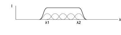
- FIG. 4 shows the integrated spectrum of pulsed laser light containing multiple central wavelengths.
- the integrated spectrum shown in FIG. 4 corresponds to the integrated spectrum for one period of the wavelength change shown in FIG. 3.
- the horizontal axis indicates wavelength ⁇
- the vertical axis indicates light intensity I.
- the dashed line indicates the spectrum of the pulsed laser light for each pulse, and each central wavelength coincides with the peak wavelength.
- FIG. 5 shows a photosensitive substrate exposed by the exposure apparatus 200.
- the photosensitive substrate is, for example, a monocrystalline silicon plate having a substantially circular disk shape.
- the exposure of the photosensitive substrate is performed for each section of scan fields SF1, SF2, etc.
- Each of the scan fields SF1, SF2 is an area in which some semiconductor chips out of a large number of semiconductor chips formed on the photosensitive substrate are formed, and corresponds to an area in which a mask pattern of one photomask is transferred in one scan.
- the numbers included in the symbols SF1 and SF2 indicate the exposure order. When describing without specifying the exposure order, the numbers are not added and the field is simply written as SF.
- the photosensitive substrate is moved so that the first scan field SF1 is irradiated with pulsed laser light, and the first scan field SF1 is exposed.
- the photosensitive substrate is moved so that the second scan field SF2 is irradiated with pulsed laser light, and the second scan field SF2 is exposed.
- the other scan fields SF are also exposed sequentially, and when the last scan field SFkmax is exposed, the exposure of the photosensitive substrate is completed.
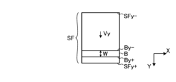
- Figures 6 to 8 show how the position of the scan field SF on the photosensitive substrate changes relative to the position of the beam cross section B of the pulsed laser light.
- the direction in which the position of the scan field SF changes is the Y-axis direction, and the direction perpendicular to the Y-axis direction is the X-axis direction.
- pulsed laser light When exposing one scan field SF, pulsed laser light is output continuously at a predetermined repetition frequency. Continuous output of pulsed laser light at a predetermined repetition frequency is called burst output. When moving the exposure position from one scan field SF to another scan field SF, the output of pulsed laser light is stopped. Therefore, burst output is repeated multiple times to expose one photosensitive substrate.
- the width of the scan field SF in the X-axis direction corresponds to the width of the beam cross section B of the pulsed laser light in the X-axis direction at the position of the workpiece table WT (see Figure 1).
- the width of the scan field SF in the Y-axis direction is greater than the width W of the beam cross section B of the pulsed laser light in the Y-axis direction at the position of the workpiece table WT.
- the procedure for scanning and exposing each scan field SF in the Y-axis direction with pulsed laser light is performed in the order of Figures 6, 7, and 8.
- the workpiece table WT is positioned so that the +Y-direction end SFy+ of the scan field SF is located a predetermined distance in the -Y direction from the position of the -Y-direction end By- of the beam cross section B.
- the workpiece table WT is accelerated in the +Y direction to a speed Vy until the +Y-direction end SFy+ of the scan field SF coincides with the position of the -Y-direction end By- of the beam cross section B.
- the scan field SF is exposed while the workpiece table WT is moved in the +Y direction so that the position of the scan field SF moves linearly at a constant speed Vy relative to the position of the beam cross section B.
- Vy the position of the scan field SF moves linearly at a constant speed
- the scan field SF moves relative to the position of the beam cross section B. If the scan field SF is used as a reference, it can also be said that the pulsed laser light scans in the -Y direction.
- Ts W/Vy
- Ns F ⁇ Ts
- the number of irradiation pulses Ns of the pulsed laser light irradiated to any one location in the scan field SF is desirably a multiple of the number of pulses N for one period of wavelength change. This ensures that any part of the scan field SF is irradiated with the number of irradiation pulses Ns of pulsed laser light having the same integrated spectrum. This reduces variation in the exposure results depending on the irradiation position, making it possible to manufacture high-quality electronic devices.
- the exposure apparatus 200 transfers the pattern of the photomask onto the photosensitive substrate at a specified reduction magnification, for example, 1/4 size.
- the size of the pattern transferred onto the photosensitive substrate may be larger or smaller than the expected size. This phenomenon can be seen as a deviation of each point on the surface of the photosensitive substrate from its original position, and since this deviation changes depending on the distance from the optical axis, it is called magnification distortion.
- magnification distortion causes enlargement or reduction, or the degree of enlargement or reduction, varies depending on the design of the exposure apparatus 200 and the settings of the optical system during exposure.
- magnification distortion can cause overlay errors between multiple layers.
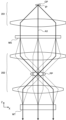
- Fig. 9 is a schematic diagram of the projection optical system 202 included in the exposure apparatus 200.
- Fig. 9 shows marginal rays of light with a target short wavelength ⁇ 1 and a target long wavelength ⁇ 2, which reach the photosensitive substrate placed on the workpiece table WT from the photomask placed on the mask stage MS.
- the target short wavelength ⁇ 1 the position of the photomask is in a conjugate relationship with the position of the photosensitive substrate, and the pattern of the photomask is transferred onto the photosensitive substrate.
- the optical system of the exposure apparatus 200 is designed so that aberration is minimized at a certain design wavelength, for example, the target short wavelength ⁇ 1.
- a certain design wavelength for example, the target short wavelength ⁇ 1.
- the direction of travel of the light differs from when light of the design wavelength is used, due to the wavelength dependency of the refraction angle. This difference is called chromatic aberration.
- Chromatic aberration has the effect of shifting the image both in the direction of the optical axis AX and in the direction perpendicular to the optical axis AX.
- the chromatic aberration component that shifts the image in the direction of the optical axis AX is called longitudinal chromatic aberration
- the chromatic aberration component that shifts the image in the direction perpendicular to the optical axis AX is called transverse chromatic aberration.
- longitudinal chromatic aberration is indicated by ⁇ z
- transverse chromatic aberration is indicated by ⁇ x.
- Magnification chromatic aberration Figure 10 shows how the image formed on the photosensitive substrate by the projection optical system 202 shown in Figure 9 is distorted.
- the dashed line shows the image with the target short wavelength ⁇ 1
- the solid line shows the image with the target long wavelength ⁇ 2.
- the lateral chromatic aberration ⁇ x may vary depending on the distance of the object point or image point from the optical axis AX, and may cause magnification distortion.
- the magnification distortion caused by the lateral chromatic aberration ⁇ x is called magnification chromatic aberration.
- a double-telecentric optical system has the advantage that, for example, movement of the photosensitive substrate or photomask in the direction of the optical axis AX does not cause magnification distortion.
- the position of the photomask and the position of the photosensitive substrate are in a conjugate relationship.
- the projection optical system 202 shown in FIG. 9 is double-telecentric for light of wavelength ⁇ 1, but may not be double-telecentric for light of wavelength ⁇ 2.
- Fig. 11 is a schematic diagram of an optical system including a part of an illumination optical system 201 and a projection optical system 202 that is double-telecentric.
- the position of the photomask and the position of the photosensitive substrate are in a conjugate relationship.
- the pupil IP of the illumination optical system 201 is located at a conjugate point CP of the pupil PP of the projection optical system 202.
- Fig. 11 shows an ideal state with no magnification telecentric error. In this case, the size of the image does not change even if the photosensitive substrate moves up and down in the direction of the optical axis AX.
- the pupil IP of the illumination optical system 201 shifts in the direction of the arrow D1 along the optical axis AX of the pulsed laser light from the conjugate point CP with the pupil PP of the projection optical system 202.
- the chief ray changes from the ideal state ID to the actual state RE, and the angle of incidence with respect to the photosensitive substrate becomes non-perpendicular.
- the size of the image changes.
- the pupil IP of the illumination optical system 201 corresponds to the first pupil in this disclosure
- the pupil PP of the projection optical system 202 corresponds to the second pupil in this disclosure
- the position of the conjugate point CP corresponds to the reference position in this disclosure.
- Figures 13 to 15 show how the image formed on the photosensitive substrate changes due to the optical system shown in Figure 12.
- Position Z0 in the Z direction is the best focus position of the projection optical system 202, and at position Z0, the image formed on the photosensitive substrate does not change before and after the pupil IP shifts. However, at position Z0+, which is displaced from position Z0 in the Z direction, the image changes from the ideal state ID to the actual state RE and becomes smaller, and conversely, at position Z0-, which is displaced from Z0 in the -Z direction, the image becomes larger.
- FIG. 16 shows the change in the chief ray when the pupil IP of the illumination optical system 201 in the optical system shown in FIG. 11 shifts in the opposite direction to that in FIG. 12.
- the pupil IP of the illumination optical system 201 shifts in the direction of the arrow D2 along the optical axis AX of the pulsed laser light from the conjugate point CP with the pupil PP of the projection optical system 202.
- Figures 17 to 19 show how the image formed on the photosensitive substrate changes due to the optical system shown in Figure 16.
- the image formed on the photosensitive substrate does not change before and after the pupil IP shifts.
- the image changes from the ideal state ID to the actual state RE and becomes larger, and conversely, at position Z0-, which is displaced in the -Z direction from Z0, the image becomes smaller.
- magnification telecentric error the error caused by the enlargement or reduction of the image when the photosensitive substrate is shifted from the best focus position. Since the direction of travel of the chief ray can be controlled by the position of the pupil IP of the illumination optical system 201, it is possible to control the magnitude of the magnification telecentric error.
- Fig. 20 is a schematic diagram showing a part of a marginal ray of a pulsed laser beam incident on the workpiece table WT when longitudinal chromatic aberration ⁇ z and transverse chromatic aberration ⁇ x are generated.
- Fig. 20 corresponds to a part extracted from Fig. 9.
- Fig. 20 includes a marginal ray of a target short wavelength ⁇ 1 and a marginal ray of a target long wavelength ⁇ 2, and the tip of each marginal ray indicates the best focus position of each wavelength.
- FIG. 21 shows a schematic of the imaging area of each wavelength of the pulsed laser light shown in FIG. 20.
- the image generated by the pulsed laser light does not suddenly disappear when it is displaced from the best focus position, but the contrast gradually decreases within an imaging area of a certain size, and no image is formed when it is moved out of the imaging area.
- the imaging area does not have a clear boundary, but is shown as an ellipse for convenience. Due to the longitudinal chromatic aberration ⁇ z, for example, the target long wavelength ⁇ 2 is imaged at a position shifted in the -Z direction from the target short wavelength ⁇ 1.
- the transverse chromatic aberration ⁇ x occurs in opposite directions with the optical axis AX as the center, and for example, the target long wavelength ⁇ 2 is imaged at a position shifted outward from the optical axis AX as the center.
- FIG. 22 is a cross-sectional view showing a resist profile when a photosensitive substrate exposed to the pulsed laser light shown in FIGS. 20 and 21 is developed.
- the photosensitive substrate includes a resist film R formed on the surface of a semiconductor substrate SUB. Because the pulsed laser light shown in FIGS. 20 and 21 has longitudinal chromatic aberration ⁇ z, good imaging performance can be obtained throughout the entire thickness direction of the resist film R, even for a thick resist film R. However, in areas away from the optical axis AX of the pulsed laser light, transverse chromatic aberration ⁇ x occurs, and the imaging positions in the X direction differ between the target short wavelength ⁇ 1 and the target long wavelength ⁇ 2. As a result, the inclination angles of the wall surfaces on both sides of the portion where the resist film R has been removed may become asymmetric.
- Figure 23 shows the image shift on a photosensitive substrate scanned and exposed with the pulsed laser light shown in Figures 20 and 21.
- the imaging position in the X direction differs between the target short wavelength ⁇ 1 and the target long wavelength ⁇ 2, and the shift is particularly noticeable at the ends away from the optical axis AX in the X and -X directions. For this reason, even with a thin resist film R, the image may shift or become blurred due to lateral chromatic aberration ⁇ x. Note that in the scanning exposure described with reference to Figures 6 to 8, the photosensitive substrate is moved in the Y direction while being irradiated with pulsed laser light, so the lateral chromatic aberration in the Y direction is averaged.
- WO 2021/110343 discloses shifting a pattern in advance depending on its position in the photomask or inserting an auxiliary pattern (sub-resolution assist feature: SRAF).
- SRAF sub-resolution assist feature
- Such photomasks are optimized for specific spectral parameters, and if the spectral parameters change even when exposing the same pattern, a different photomask must be designed and manufactured.
- there is a lower limit to the dimensions of the auxiliary pattern due to manufacturing constraints, and if the dimensions of the auxiliary pattern are too large, the effect of the auxiliary pattern may be excessive.
- the embodiment described below relates to suppressing lateral chromatic aberration by generating a telecentric error of magnification - ⁇ x to offset the lateral chromatic aberration ⁇ x when exposing using multiple wavelengths.
- Fig. 24 is a schematic diagram showing a part of the chief ray of the pulsed laser light incident on the workpiece table WT when a magnification telecentric error occurs.
- Fig. 24 corresponds to a part extracted from Fig. 12.
- the chief ray of the target short wavelength ⁇ 1 and the chief ray of the target long wavelength ⁇ 2 are common.
- FIG. 25 shows a schematic of the imaging area of each wavelength of the pulsed laser light shown in FIG. 24.
- the target long wavelength ⁇ 2 Due to longitudinal chromatic aberration ⁇ z, for example, the target long wavelength ⁇ 2 is imaged at a position shifted in the -Z direction from the target short wavelength ⁇ 1.
- the angle of incidence of the chief ray with respect to the photosensitive substrate becomes non-perpendicular due to a shift in the pupil IP of the illumination optical system 201, a magnification telecentric error ⁇ x determined by the longitudinal chromatic aberration ⁇ z and the angle of incidence occurs between the target short wavelength ⁇ 1 and the target long wavelength ⁇ 2.
- FIG. 26 shows a schematic diagram of the imaging area of light of each wavelength when the transverse chromatic aberration ⁇ x is taken into account in the pulsed laser light shown in FIG. 24.
- the imaging area shown in FIG. 26 corresponds to the sum of the transverse chromatic aberration ⁇ x shown in FIG. 21 and the magnification telecentric error ⁇ x shown in FIG. 25.
- the transverse chromatic aberration ⁇ x and the magnification telecentric error ⁇ x act in the same direction, resulting in a large magnification distortion ⁇ x+ ⁇ x.
- FIG. 27 is a schematic diagram showing a portion of the chief ray of the pulsed laser light incident on the workpiece table WT when a magnification telecentric error - ⁇ x occurs in the opposite direction to that in FIG. 24.
- FIG. 27 corresponds to an excerpt of FIG. 16.
- the chief ray of the target short wavelength ⁇ 1 and the chief ray of the target long wavelength ⁇ 2 are common.
- FIG. 28 shows a schematic of the imaging area of the light of each wavelength of the pulsed laser light shown in FIG. 27. Due to longitudinal chromatic aberration ⁇ z, for example, the target long wavelength ⁇ 2 is imaged at a position shifted in the -Z direction from the target short wavelength ⁇ 1. On the other hand, even if it is assumed that there is no transverse chromatic aberration or that it is extremely slight, if the angle of incidence of the chief ray to the photosensitive substrate becomes non-perpendicular due to the shift of the pupil IP of the illumination optical system 201, a magnification telecentric error - ⁇ x determined by the longitudinal chromatic aberration ⁇ z and the angle of incidence occurs between the target short wavelength ⁇ 1 and the target long wavelength ⁇ 2.
- magnification telecentric error ⁇ x in FIG. 25 and the magnification telecentric error - ⁇ x in FIG. 28 occur in the opposite direction.
- Figure 29 shows a schematic diagram of the imaging area of light of each wavelength when the transverse chromatic aberration ⁇ x is taken into account in the pulsed laser light shown in Figure 27.
- the imaging area shown in Figure 29 corresponds to the sum of the transverse chromatic aberration ⁇ x shown in Figure 21 and the magnification telecentric error - ⁇ x shown in Figure 28.
- the transverse chromatic aberration ⁇ x and the magnification telecentric error - ⁇ x are caused to act in opposite directions, thereby canceling each other out, and the deviation of the imaging position on the photosensitive substrate caused by the transverse chromatic aberration ⁇ x can be reduced by the magnification telecentric error - ⁇ x. This reduces the magnification distortion.
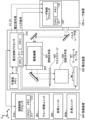
- the exposure apparatus 200 includes a measurement unit 303, and the illumination optical system 201 includes a drive mechanism 203.
- the measurement unit 303 includes a stage on which the exposed photosensitive substrate is mounted, and a sensor that observes the exposure state of the photosensitive substrate.
- the measurement unit 303 drives the stage under the control of the exposure control processor 210, measures the pattern formed on the photosensitive substrate with the sensor, and measures the magnification distortion from this pattern.
- the measurement unit 303 corresponds to the measurement sensor in this disclosure.
- the driving mechanism 203 includes an actuator that drives at least one optical element included in the illumination optical system 201 in order to adjust the position of the pupil IP of the illumination optical system 201.
- the driving mechanism 203 is configured to be able to adjust the position of the pupil IP of the illumination optical system 201 in both the direction of arrow D1 approaching the pupil PP from the conjugate point CP with the pupil PP of the projection optical system 202 along the optical axis AX of the pulsed laser light, and the direction of arrow D2 moving away from the pupil PP.
- the driving mechanism 203 operates under the control of the exposure control processor 210.
- FIG. 31 conceptually illustrates a first example of an illumination optical system 201 in which the position of the pupil IP can be moved.
- the illumination optical system 201 includes a beam shaping/uniformization optical system 204, a mechanical aperture 205, and a pupil position adjustment optical system 206a.
- the beam shaping/homogenizing optical system 204 is an optical system that shapes and homogenizes pulsed laser light having, for example, a nearly rectangular beam cross section and a Gaussian light intensity distribution into a desired beam cross section and a uniform light intensity distribution.
- Mechanical aperture 205 is a mechanical diaphragm and is disposed near the pupil IP. Mechanical aperture 205 corresponds to the mechanical diaphragm in this disclosure.
- the pupil position adjustment optical system 206a is an optical system that irradiates the light emitted from the pupil IP onto a photomask. At least one of the optical elements included in the pupil position adjustment optical system 206a is moved by the drive mechanism 203, so that the position of the pupil IP moves in the direction of the optical axis AX.
- FIG. 32 conceptually illustrates a second example of an illumination optical system 201 in which the position of the pupil IP can be moved.
- the illumination optical system 201 includes a beam shaping/homogenizing optical system 204, a diffractive optical element 207, and a pupil position adjustment optical system 206b.
- the diffractive optical element 207 is an optical element that has numerous irregularities on its surface and splits the light that passes through it into multiple diffracted light beams.
- the irregularities on the surface of the diffractive optical element 207 are designed to emit each diffracted light beam in a desired direction.
- the diffracted light beams emitted from the diffractive optical element 207 enter the pupil position adjustment optical system 206b.
- the pupil position adjustment optical system 206b focuses the diffracted light beam onto the pupil IP.
- the focusing position i.e., the position of the pupil IP, moves in the direction of the optical axis AX.
- FIG. 33 conceptually illustrates a third example of an illumination optical system 201 in which the position of the pupil IP can be moved.
- the illumination optical system 201 includes a beam shaping/uniformizing optical system 204, a micromirror array 208, a mirror 209, and a pupil position adjustment optical system 206c.
- Micromirror array 208 is an optical element that includes a large number of mirrors, each with an adjustable tilt, and splits the light incident on micromirror array 208 into multiple reflected light beams.
- the tilt of the mirrors included in micromirror array 208 is adjusted so that each reflected light beam is emitted in a desired direction.
- the reflected light beams emitted from micromirror array 208 enter pupil position adjustment optical system 206c via mirror 209.
- the pupil position adjustment optical system 206c focuses the reflected light beam onto the pupil IP.
- the focusing position i.e., the position of the pupil IP, moves in the direction of the optical axis AX.
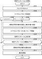
- Operation (Magnification Distortion Correction) 34 is a flowchart showing a process for correcting magnification distortion in the first embodiment.
- the exposure control processor 210 corrects the magnification distortion by controlling the drive mechanism 203 so as to reduce the deviation of the imaging position caused by the lateral chromatic aberration ⁇ x as follows, based on the magnification distortion measured by the measurement unit 303.
- the exposure control processor 210 controls a transport device (not shown) to set the photomask on the mask stage MS of the exposure device 200.
- the exposure control processor 210 sets the spectral parameters of the pulsed laser light including multiple central wavelengths.
- the spectral parameters include, for example, a target short wavelength ⁇ 1 and a target long wavelength ⁇ 2.
- the spectral parameters may include a wavelength difference between the target short wavelength ⁇ 1 and the target long wavelength ⁇ 2.
- the spectral parameters may further include the number of pulses N for one period of wavelength change.
- the exposure control processor 210 sets the value of counter j, which identifies the position of the pupil IP of the illumination optical system 201, to an initial value of 1.
- the exposure control processor 210 controls the drive mechanism 203 so that the position of the pupil IP of the illumination optical system 201 becomes the jth value.
- the exposure control processor 210 transmits various parameters and signals to the laser control processor 130 so that the laser oscillates according to the spectral parameters set in S103.
- the exposure control processor 210 also controls the mask stage MS and the workpiece table WT so that the image of the photomask formed by the pulsed laser light containing multiple central wavelengths is transferred onto the photosensitive substrate, and the photosensitive substrate is exposed.
- the photosensitive substrate exposed here may be a photosensitive substrate for measurement, separate from the photosensitive substrate for manufacturing semiconductor devices.
- the exposure control processor 210 controls the measurement unit 303 to measure the magnification distortion from the pattern formed on the exposed photosensitive substrate.
- the exposure control processor 210 determines whether the magnification distortion is equal to or less than the threshold value. If the magnification distortion exceeds the threshold value (S108: NO), the exposure control processor 210 proceeds to S109. If the magnification distortion is equal to or less than the threshold value (S108: YES), the exposure control processor 210 proceeds to S110.
- the exposure control processor 210 adds 1 to the value of counter j to update j, and then returns to S105.
- An upper limit may be set for the value of counter j, and the exposure control processor 210 may end the processing of this flowchart when j reaches the upper limit.
- the exposure control processor 210 determines the position of the pupil IP of the illumination optical system 201 to be the jth value at which the magnification distortion is equal to or less than the threshold value.
- the exposure control processor 210 places a photosensitive substrate for manufacturing a semiconductor device on the workpiece table WT, starts exposure, and ends the processing of this flowchart.
- the exposure system includes an illumination optical system 201 that illuminates a photomask with a pulsed laser beam including a target short wavelength ⁇ 1 and a target long wavelength ⁇ 2, and a projection optical system 202 that illuminates a photosensitive substrate with the pulsed laser beam that has passed through the photomask to project an image of the photomask.
- the position of the pupil IP of the illumination optical system 201 is shifted from the conjugate point CP of the pupil PP of the projection optical system 202 in the direction of an arrow D2 that reduces the deviation of the imaging position on the photosensitive substrate due to the lateral chromatic aberration ⁇ x by the magnification telecentric error - ⁇ x.
- the position of the pupil IP of the illumination optical system 201 is shifted, and the deviation in the imaging position due to the lateral chromatic aberration ⁇ x can be reduced by the magnification telecentric error - ⁇ x, so that even a thick resist film can be processed with high precision.
- the deviation in the imaging position by designing a photomask there is a high degree of freedom in the design of the photomask.
- the position of the pupil IP is shifted from the conjugate point CP of the pupil PP along the optical axis AX of the pulsed laser light.
- the exposure system includes a driving mechanism 203 that adjusts the position of the pupil IP, and an exposure control processor 210 that controls the driving mechanism 203 so as to reduce the deviation of the imaging position due to the lateral chromatic aberration ⁇ x.
- the driving mechanism 203 is configured to be able to adjust the position of the pupil IP along the optical axis AX of the pulsed laser light in both the direction of arrow D1, which moves from the conjugate point CP of the pupil PP toward the pupil PP, and the direction of arrow D2, which moves away from the pupil PP.
- the exposure system includes a measurement unit 303 that measures the pattern formed by projection onto the photosensitive substrate, and the exposure control processor 210 controls the drive mechanism 203 based on the measurement results of the measurement unit 303.
- magnification distortion This allows magnification distortion to be suppressed with high precision based on the measurement results of the measurement unit 303.
- the measurement unit 303 measures the magnification distortion of the pattern formed by projection onto the photosensitive substrate, and the exposure control processor 210 controls the drive mechanism 203 based on the magnification distortion.
- the first embodiment is similar to the comparative example.
- Exposure system that determines the position of the pupil IP of the illumination optical system 201 based on spectral parameters
- Configuration Fig. 35 shows an outline of the configuration of an exposure system in the second embodiment.
- the exposure apparatus 200 includes a non-volatile memory 213.
- the non-volatile memory 213 stores a correction table 213a (see Fig. 37) that associates the spectral parameters with the position of the pupil IP of the illumination optical system 201.
- the non-volatile memory 213 is accessible from the exposure control processor 210.
- FIG. 36 is a flowchart showing the process of creating the correction table 213a in the second embodiment.
- the exposure control processor 210 creates the correction table 213a as follows.
- the exposure control processor 210 controls a transport device (not shown) to set the photomask on the mask stage MS of the exposure device 200. This is similar to the process included in the correction of magnification distortion in the first embodiment.
- the exposure control processor 210 sets the value of counter i, which specifies the spectral parameter, to an initial value of 1.
- the exposure control processor 210 sets the spectral parameter to the i-th value.
- the processes from S104 to S109 are similar to those included in the correction of magnification distortion in the first embodiment, and the exposure control processor 210 searches for the position of the pupil IP where the magnification distortion is equal to or less than a threshold value for the given spectral parameters. If the magnification distortion is equal to or less than the threshold value (S108: YES), the exposure control processor 210 proceeds to S112a.
- the exposure control processor 210 stores in the correction table 213a of the non-volatile memory 213 the correspondence between the i-th spectral parameter and the j-th position of the pupil IP of the illumination optical system 201 where the magnification distortion is equal to or less than a threshold value, based on the measurement result of the magnification distortion by the measurement unit 303.
- the exposure control processor 210 determines whether the value of counter i has reached the maximum value imax. If the value of counter i has reached the maximum value imax (S113a: YES), the exposure control processor 210 ends the processing of this flowchart. If the value of counter i is less than the maximum value imax (S113a: NO), the exposure control processor 210 proceeds to S114a.
- the exposure control processor 210 adds 1 to the value of counter i to update i, and then returns to S103a.
- FIG. 37 shows an example of the correction table 213a stored in the non-volatile memory 213.
- the correction table 213a is a data table that stores the spectral parameters S1 to Simax and the positions P1 to Pimax of the pupil IP of the illumination optical system 201 at which the magnification distortion is equal to or less than a threshold value, corresponding to the values 1 to imax of the counter i.
- the positions P1 to Pimax of the pupil IP correspond to the control parameters in this disclosure.
- a different correction table 213a may be created for each photomask.
- Fig. 38 is a flowchart showing the process of correcting magnification distortion in the second embodiment.
- the exposure control processor 210 controls the drive mechanism 203 based on the spectral parameters of the pulsed laser beam as follows. It is assumed that the photomask has already been set on the mask stage MS.
- the exposure control processor 210 sets the spectral parameters of the pulsed laser light. This is the same as in the first embodiment.
- the exposure control processor 210 sets the position of the pupil IP of the illumination optical system 201 corresponding to the set spectral parameters to the value read from the correction table 213a, and controls the drive mechanism 203.
- the exposure control processor 210 places the photosensitive substrate on the workpiece table WT, starts exposure, and ends the processing of this flowchart.
- the second embodiment is similar to the first embodiment.
- the exposure control processor 210 can access the correction table 213 a that associates the wavelength difference between the target short wavelength ⁇ 1 and the target long wavelength ⁇ 2 with the positions P1 to Pimax of the pupil IP, and reads out the position of the pupil IP corresponding to the wavelength difference from the correction table 213 a to control the drive mechanism 203.
- the exposure control processor 210 controls the driving mechanism 203 based on the spectral parameters of the pulsed laser light.
- the driving mechanism 203 may be controlled using a function of the spectral parameters and the control parameters of the driving mechanism 203, without being limited to using the correction table 213a. In this way, since the control is based on the spectral parameters, the process for controlling the driving mechanism 203 can be simplified.
- the exposure control processor 210 can access a correction table 213a that associates the spectral parameters S1 to Simax with the positions P1 to Pimax of the pupil IP, and reads out the positions of the pupil IP corresponding to the spectral parameters from the correction table 213a to control the drive mechanism 203.
- the exposure system includes a measurement unit 303 that measures the pattern formed by projection onto the photosensitive substrate, and the exposure control processor 210 stores the correspondence between the spectral parameters S1 to Simax and the positions P1 to Pimax of the pupil IP in the correction table 213a based on the measurement results of the measurement unit 303.
- the measurement unit 303 measures the magnification distortion of the pattern formed by projection onto the photosensitive substrate, and the exposure control processor 210 stores in the correction table 213a the correspondence between each of the spectral parameters S1 to Simax and the positions P1 to Pimax of the pupil IP at which the magnification distortion is equal to or less than a threshold value.
- the exposure system includes a developing apparatus 300 separate from the exposure apparatus 200.
- the developing apparatus 300 includes a wafer moving unit 301, a processing unit 302, a measuring unit 303b, and a development control processor 310.
- the wafer movement unit 301 is a device that transfers the photosensitive substrate between the exposure device 200 and the developing device 300, and moves the photosensitive substrate inside the developing device 300.
- the processing unit 302 is a device that applies a resist film to a photosensitive substrate, performs post-exposure baking (PEB) of the photosensitive substrate exposed inside the exposure device 200, supplies a developer, cleans, dries, and performs post-development baking (PDB), etc.
- PEB post-exposure baking
- the measurement unit 303b is a device that measures the pattern formed on the photosensitive substrate by exposure and development.
- the measurement unit 303b may be a cross-sectional inspection SEM that measures the resist profile, a pattern position measurement device that measures the overlay error, or a device that measures the magnification distortion from the planar shape of the resist film.
- the measurement unit 303b corresponds to the measurement sensor in this disclosure.
- the measurement unit 303b may be provided separately from the development device 300.
- the development control processor 310 is a processing device that includes a memory 312 in which a control program is stored, and a CPU 311 that executes the control program.
- the development control processor 310 is specially configured or programmed to execute the various processes included in this disclosure.
- the exposure apparatus 200 does not need to include the measurement unit 303 described in the first embodiment.
- Operation (Magnification Distortion Correction) 40 is a flowchart showing a process for correcting magnification distortion in the third embodiment.
- the development control processor 310 develops and measures the photosensitive substrate, and the exposure control processor 210 corrects the magnification distortion by controlling the drive mechanism 203 based on the measurement results so as to reduce the deviation of the imaging position due to the lateral chromatic aberration ⁇ x.
- S101 to S105 is the same as in the first embodiment.
- the exposure control processor 210 not only controls the exposure device 200 to expose the photosensitive substrate, but also the development control processor 310 controls the development device 300 so that the exposed photosensitive substrate is developed by the development device 300.
- the development control processor 310 controls the measurement unit 303b to measure the resist profile, overlay error, or magnification distortion of the exposed and developed photosensitive substrate.
- the resist profile is measured as a larger value, for example, the more asymmetric the inclination angle of the wall surface of the resist film is.
- the exposure control processor 210 receives the measurement results of the resist profile, overlay error, or magnification distortion measured by the measurement unit 303b from the development control processor 310, and determines whether the measurement results are equal to or less than a threshold value. If the measurement results exceed the threshold value (S108b: NO), the exposure control processor 210 proceeds to S109. If the measurement results are equal to or less than the threshold value (S108b: YES), the exposure control processor 210 proceeds to S110.
- the processes of S109, S110, and S111 are the same as those in the first embodiment.
- the third embodiment is similar to the first embodiment.
- the exposure system may include a measurement unit 303b that is separate from the exposure apparatus 200.
- the exposure system includes a measurement unit 303b that measures a pattern formed by projection onto a photosensitive substrate and development, and the exposure control processor 210 controls the drive mechanism 203 based on the measurement results of the measurement unit 303b.
- the measurement unit 303b measures the resist profile of the photosensitive substrate, and the exposure control processor 210 controls the drive mechanism 203 based on the asymmetry of the resist profile.
- the drive mechanism 203 is controlled based on the asymmetry of the resist profile of the developed photosensitive substrate, so that the asymmetry of the resist profile can be reduced and products can be manufactured.
- the measurement unit 303b measures the overlay error between multiple layers formed by multiple projections and developments, and the exposure control processor 210 controls the drive mechanism 203 based on the overlay error.
- the drive mechanism 203 is controlled based on the overlay error of the developed photosensitive substrate, making it possible to manufacture products with small overlay errors.
- the measurement unit 303b measures the magnification distortion from the planar shape of the resist film contained in the photosensitive substrate, and the exposure control processor 210 controls the drive mechanism 203 based on the magnification distortion.
- the driving mechanism 203 is controlled based on the magnification distortion measured from the planar shape of the resist film on the developed photosensitive substrate, making it possible to manufacture products with small magnification distortion.
Landscapes
- Physics & Mathematics (AREA)
- General Physics & Mathematics (AREA)
- Exposure And Positioning Against Photoresist Photosensitive Materials (AREA)
Priority Applications (4)
| Application Number | Priority Date | Filing Date | Title |
|---|---|---|---|
| JP2024565455A JPWO2024134780A1 (https=) | 2022-12-20 | 2022-12-20 | |
| CN202280101662.0A CN120153322A (zh) | 2022-12-20 | 2022-12-20 | 曝光系统及电子器件的制造方法 |
| PCT/JP2022/046927 WO2024134780A1 (ja) | 2022-12-20 | 2022-12-20 | 露光システム、及び電子デバイスの製造方法 |
| US19/199,798 US20250264804A1 (en) | 2022-12-20 | 2025-05-06 | Exposure system and method of manufacturing electronic device |
Applications Claiming Priority (1)
| Application Number | Priority Date | Filing Date | Title |
|---|---|---|---|
| PCT/JP2022/046927 WO2024134780A1 (ja) | 2022-12-20 | 2022-12-20 | 露光システム、及び電子デバイスの製造方法 |
Related Child Applications (1)
| Application Number | Title | Priority Date | Filing Date |
|---|---|---|---|
| US19/199,798 Continuation US20250264804A1 (en) | 2022-12-20 | 2025-05-06 | Exposure system and method of manufacturing electronic device |
Publications (1)
| Publication Number | Publication Date |
|---|---|
| WO2024134780A1 true WO2024134780A1 (ja) | 2024-06-27 |
Family
ID=91588120
Family Applications (1)
| Application Number | Title | Priority Date | Filing Date |
|---|---|---|---|
| PCT/JP2022/046927 Ceased WO2024134780A1 (ja) | 2022-12-20 | 2022-12-20 | 露光システム、及び電子デバイスの製造方法 |
Country Status (4)
| Country | Link |
|---|---|
| US (1) | US20250264804A1 (https=) |
| JP (1) | JPWO2024134780A1 (https=) |
| CN (1) | CN120153322A (https=) |
| WO (1) | WO2024134780A1 (https=) |
Citations (4)
| Publication number | Priority date | Publication date | Assignee | Title |
|---|---|---|---|---|
| JP2002222757A (ja) * | 2001-01-26 | 2002-08-09 | Canon Inc | 露光装置、デバイス製造方法及びデバイス |
| JP2002313691A (ja) * | 2001-04-10 | 2002-10-25 | Sony Corp | 露光マスクの製造方法および露光マスク |
| JP2019139142A (ja) * | 2018-02-14 | 2019-08-22 | 株式会社ピーエムティー | 露光装置及び露光方法 |
| JP2020021084A (ja) * | 2019-09-27 | 2020-02-06 | キヤノン株式会社 | 照明光学系、露光装置、および物品の製造方法 |
-
2022
- 2022-12-20 JP JP2024565455A patent/JPWO2024134780A1/ja active Pending
- 2022-12-20 WO PCT/JP2022/046927 patent/WO2024134780A1/ja not_active Ceased
- 2022-12-20 CN CN202280101662.0A patent/CN120153322A/zh active Pending
-
2025
- 2025-05-06 US US19/199,798 patent/US20250264804A1/en active Pending
Patent Citations (4)
| Publication number | Priority date | Publication date | Assignee | Title |
|---|---|---|---|---|
| JP2002222757A (ja) * | 2001-01-26 | 2002-08-09 | Canon Inc | 露光装置、デバイス製造方法及びデバイス |
| JP2002313691A (ja) * | 2001-04-10 | 2002-10-25 | Sony Corp | 露光マスクの製造方法および露光マスク |
| JP2019139142A (ja) * | 2018-02-14 | 2019-08-22 | 株式会社ピーエムティー | 露光装置及び露光方法 |
| JP2020021084A (ja) * | 2019-09-27 | 2020-02-06 | キヤノン株式会社 | 照明光学系、露光装置、および物品の製造方法 |
Also Published As
| Publication number | Publication date |
|---|---|
| JPWO2024134780A1 (https=) | 2024-06-27 |
| CN120153322A (zh) | 2025-06-13 |
| US20250264804A1 (en) | 2025-08-21 |
Similar Documents
| Publication | Publication Date | Title |
|---|---|---|
| US7817249B2 (en) | Exposure method and apparatus, and device producing method using two light beams to correct non-rotationally symmetric aberration | |
| TWI706440B (zh) | 光微影設備及光微影方法 | |
| KR101302244B1 (ko) | 노광 장치, 노광 방법 및 디바이스 제조 방법, 및 시스템 | |
| CN1289967C (zh) | 光刻投射装置以及器件制造方法 | |
| US8111378B2 (en) | Exposure method and apparatus, and device production method | |
| CN112119355B (zh) | 检查设备的照射源、检查设备和检查方法 | |
| US12300962B2 (en) | Laser device and electronic device manufacturing method | |
| US6455862B1 (en) | Lithographic projection apparatus | |
| JP2001345245A (ja) | 露光方法及び露光装置並びにデバイス製造方法 | |
| TWI880958B (zh) | 微影設備及偵測輻射光束之方法 | |
| US7826036B2 (en) | Scanning exposure apparatus and method of manufacturing device | |
| TWI803761B (zh) | 補償重複率偏差引起之波長誤差之方法 | |
| JP4340266B2 (ja) | リソグラフィにおける粗密バイアスを制御するための方法および装置 | |
| JP5739837B2 (ja) | 露光装置、露光方法及びデバイス製造方法 | |
| CN114730134B (zh) | 用于控制辐射脉冲的突发的辐射系统 | |
| CN117397134A (zh) | 波长控制方法、激光装置和电子器件的制造方法 | |
| US8416389B2 (en) | Exposure apparatus and method of manufacturing device | |
| KR20080050305A (ko) | 노광장치 및 디바이스의 제조방법 | |
| WO2024134780A1 (ja) | 露光システム、及び電子デバイスの製造方法 | |
| CN116034522A (zh) | 激光装置和电子器件的制造方法 | |
| JP2007142052A (ja) | 露光装置、レーザ光源、露光方法、及びデバイス製造方法 | |
| JP4100038B2 (ja) | 露光方法および露光装置 | |
| JP2005005407A (ja) | 光源装置、露光装置、及び光源装置の制御方法 | |
| US20250060683A1 (en) | Photosensitive substrate developing method, photomask creating method, and electronic device manufacturing method | |
| CN114342564A (zh) | 改进的高次谐波生成装置 |
Legal Events
| Date | Code | Title | Description |
|---|---|---|---|
| 121 | Ep: the epo has been informed by wipo that ep was designated in this application |
Ref document number: 22969169 Country of ref document: EP Kind code of ref document: A1 |
|
| WWE | Wipo information: entry into national phase |
Ref document number: 202280101662.0 Country of ref document: CN |
|
| WWE | Wipo information: entry into national phase |
Ref document number: 2024565455 Country of ref document: JP |
|
| WWP | Wipo information: published in national office |
Ref document number: 202280101662.0 Country of ref document: CN |
|
| NENP | Non-entry into the national phase |
Ref country code: DE |
|
| 122 | Ep: pct application non-entry in european phase |
Ref document number: 22969169 Country of ref document: EP Kind code of ref document: A1 |