WO2024128015A1 - 半導体装置の製造方法、およびシート材剥離装置 - Google Patents
半導体装置の製造方法、およびシート材剥離装置 Download PDFInfo
- Publication number
- WO2024128015A1 WO2024128015A1 PCT/JP2023/042944 JP2023042944W WO2024128015A1 WO 2024128015 A1 WO2024128015 A1 WO 2024128015A1 JP 2023042944 W JP2023042944 W JP 2023042944W WO 2024128015 A1 WO2024128015 A1 WO 2024128015A1
- Authority
- WO
- WIPO (PCT)
- Prior art keywords
- wafer
- main surface
- sheet material
- peeling
- semiconductor device
- Prior art date
- Legal status (The legal status is an assumption and is not a legal conclusion. Google has not performed a legal analysis and makes no representation as to the accuracy of the status listed.)
- Ceased
Links
Images






Classifications
-
- H—ELECTRICITY
- H10—SEMICONDUCTOR DEVICES; ELECTRIC SOLID-STATE DEVICES NOT OTHERWISE PROVIDED FOR
- H10P—GENERIC PROCESSES OR APPARATUS FOR THE MANUFACTURE OR TREATMENT OF DEVICES COVERED BY CLASS H10
- H10P52/00—Grinding, lapping or polishing of wafers, substrates or parts of devices
-
- H—ELECTRICITY
- H10—SEMICONDUCTOR DEVICES; ELECTRIC SOLID-STATE DEVICES NOT OTHERWISE PROVIDED FOR
- H10P—GENERIC PROCESSES OR APPARATUS FOR THE MANUFACTURE OR TREATMENT OF DEVICES COVERED BY CLASS H10
- H10P72/00—Handling or holding of wafers, substrates or devices during manufacture or treatment thereof
- H10P72/70—Handling or holding of wafers, substrates or devices during manufacture or treatment thereof for supporting or gripping
Definitions
- This disclosure relates to a method for manufacturing a semiconductor device and a sheet material peeling device that can be used in the manufacturing method.
- Patent Document 1 discloses a SiC semiconductor device having a layered structure including a SiC semiconductor substrate and a SiC epitaxial layer, a first main surface (element formation surface) formed by the SiC epitaxial layer, and a SiC semiconductor layer having a side surface formed by the SiC semiconductor substrate and the SiC epitaxial layer, and a modification line formed on the side surface in a portion of the SiC semiconductor substrate spaced apart from the SiC epitaxial layer and modified to have properties different from those of the SiC semiconductor substrate.
- a method for manufacturing a semiconductor device includes a step of attaching a sheet material to a first main surface of a wafer having a hexagonal close-packed structure on which an element structure is formed, a processing step of processing a second main surface opposite to the first main surface, and a peeling step of peeling the sheet material from the first main surface along a direction that avoids a predetermined crystal direction after the processing step, the predetermined crystal direction including the [11-20] direction and the [1-100] direction of the wafer, as well as crystal directions equivalent thereto.
- the sheet material peeling device is a sheet material peeling device used in the manufacturing method of the semiconductor device, and includes a peeling unit capable of setting the wafer to which the sheet material is attached, and peeling the sheet material from the set wafer with the adhesive tape by moving the adhesive tape along a first direction, a tape supplying unit that supplies the adhesive tape onto the peeling unit, a tape recovery unit that recovers the used adhesive tape, and a wafer supplying unit that adjusts the orientation of the wafer so that the predetermined crystal direction is inclined with respect to the first direction, and supplies the wafer onto the peeling unit.
- the method for manufacturing a semiconductor device according to one embodiment of the present disclosure can prevent damage to the wafer when the sheet material is peeled off.
- FIG. 1 is a diagram showing a unit cell of a 4H—SiC single crystal applied to an embodiment of the present disclosure.
- FIG. 2 is a plan view showing the silicon surface of a unit cell of the 4H—SiC single crystal of FIG.
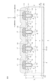
- FIG. 3 is a schematic cross-sectional view of a semiconductor device according to an embodiment of the present disclosure.
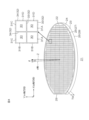
- FIG. 4 is a perspective view showing a SiC semiconductor wafer used in the manufacture of the semiconductor device.
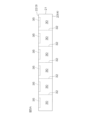
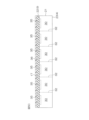
- FIG. 5A is a diagram for explaining a method for manufacturing a semiconductor device according to an embodiment of the present disclosure.
- FIG. 5B is a diagram showing the next step of FIG. 5A.
- FIG. 5C is a diagram showing the next step of FIG. 5B.
- FIG. 5D is a diagram showing the next step of FIG.
- FIG. 5E is a diagram showing the next step of FIG. 5D.
- FIG. 6 is a schematic plan view of a sheet material peeling device according to an embodiment of the present disclosure.
- FIG. 7 is a schematic cross-sectional view of a sheet material peeling device according to an embodiment of the present disclosure.
- FIG. 8 is a diagram showing steps related to adjusting the orientation of the SiC semiconductor wafer.
- FIG. 9 is a diagram showing steps related to adjusting the orientation of the SiC semiconductor wafer.
- a SiC (silicon carbide) single crystal made of a hexagonal crystal (hexagonal close-packed structure) is applied.
- the SiC single crystal made of a hexagonal crystal has a plurality of polytypes including 2H (Hexagonal)-SiC single crystal, 4H-SiC single crystal, and 6H-SiC single crystal depending on the period of the atomic arrangement.
- an example in which a 4H-SiC single crystal is applied will be described, but other polytypes are not excluded from the present disclosure.
- Figure 1 is a diagram showing a unit cell of 4H-SiC single crystal (hereinafter simply referred to as a "unit cell") that is applied to an embodiment of the present disclosure.
- Figure 2 is a plan view showing the silicon surface of the unit cell shown in Figure 1.
- the unit cell includes a tetrahedral structure in which one Si atom and four C atoms are bonded in a tetrahedral arrangement (regular tetrahedral arrangement).
- the unit cell has an atomic arrangement in which four periods of tetrahedral structures are stacked.
- the unit cell has a hexagonal silicon face, a regular hexagonal carbon face, and a hexagonal prism structure with six side faces connecting the silicon face and the carbon face.
- a silicon surface is a surface terminated by Si atoms.
- one Si atom is located at each of the six vertices of a regular hexagon, and one Si atom is located at the center of the regular hexagon.
- a carbon surface is a surface terminated by C atoms.
- one C atom is located at each of the six vertices of a regular hexagon, and one C atom is located at the center of the regular hexagon.
- the crystal planes of the unit cell are defined by four coordinate axes (a1, a2, a3, c) including the a1 axis, a2 axis, a3 axis, and c axis. Of the four coordinate axes, the value of a3 is -(a1 + a2). Below, the crystal planes of a 4H-SiC single crystal are explained using the silicon surface as a reference, as an example of a hexagonal crystal termination surface.
- the a1, a2 and a3 axes are set along the arrangement direction of the nearest Si atoms (hereinafter simply referred to as the "nearest atom direction") based on the central Si atom in a planar view of the silicon surface seen from the c-axis.
- the a1, a2 and a3 axes are set at angles of 120° each, following the arrangement of the Si atoms.
- the c-axis is set in the normal direction to the silicon surface, based on the Si atom located at the center.
- the silicon surface is the (0001) surface.
- the carbon surface is the (000-1) surface.
- the side of the hexagonal prism includes six crystal planes along the nearest atom direction when viewed from the c-axis of the silicon surface. More specifically, the side of the hexagonal prism includes six crystal planes each including the two nearest Si atoms when viewed from the c-axis of the silicon surface.
- the side of the hexagonal prism includes, in a plan view of the silicon surface from the c-axis, the (1-100), (0-110), (-1010), (-1100), (01-10), and (10-10) planes clockwise from the tip of the a1 axis.
- the diagonal plane along the diagonal line of the hexagonal prism includes six crystal planes along an intersecting direction that intersects with the nearest-neighbor atom direction when viewed from the c-axis in a plan view of the silicon surface. More specifically, the diagonal plane of the hexagonal prism includes six crystal planes each including two non-nearest neighboring Si atoms when viewed from the c-axis in a plan view of the silicon surface. When viewed from the perspective of the Si atom located in the center, the intersecting direction of the nearest-neighbor atom direction is an orthogonal direction that is perpendicular to the nearest-neighbor atom direction.
- the diagonal faces of the hexagonal prism include the (11-20), (1-210), (-2110), (-1-120), (-12-10), and (2-1-10) faces when viewed from the c-axis of the silicon surface.
- the crystal orientation of the unit cell is defined by the normal direction of the crystal plane.
- the normal direction of the (1-100) plane is the [1-100] direction.
- the normal direction of the (0-110) plane is the [0-110] direction.
- the normal direction of the (-1010) plane is the [-1010] direction.
- the normal direction of the (-1100) plane is the [-1100] direction.
- the normal direction of the (01-10) plane is the [01-10] direction.
- the normal direction of the (10-10) plane is the [10-10] direction.
- the normal direction of the (11-20) plane is the [11-20] direction.
- the normal direction of the (1-210) plane is the [1-210] direction.
- the normal direction of the (-2110) plane is the [-2110] direction.
- the normal direction of the (-1-120) plane is the [-1-120] direction.
- the normal direction of the (-12-10) plane is the [-12-10] direction.
- the normal direction of the (2-1-10) plane is the [2-1-10] direction.
- Hexagonal crystals have six-fold symmetry, and there are equivalent crystal planes and equivalent crystal directions every 60°.
- the (1-100) plane, (0-110) plane, (-1010) plane, (-1100) plane, (01-10) plane, and (10-10) plane form equivalent crystal planes.
- the [1-100] direction, [0-110] direction, [-1010] direction, [-1100] direction, [01-10] direction, and [10-10] direction form equivalent crystal directions.
- the [11-20] direction, [1-210] direction, [-2110] direction, [-1-120] direction, [-12-10] direction, and [2-1-10] direction form equivalent crystal directions.
- the c-axis is in the [0001] direction ([000-1] direction).
- the a1-axis is in the [2-1-10] direction ([-2110] direction).
- the a2-axis is in the [-12-10] direction ([1-210] direction).
- the a3-axis is in the [-1-120] direction ([11-20] direction).
- the (0001) and (000-1) planes are collectively referred to as c-planes.
- the [0001] and [000-1] directions are collectively referred to as the c-axis direction.
- the (11-20) and (-1-120) planes are collectively referred to as a-planes.
- the [11-20] and [-1-120] directions are collectively referred to as the a-axis direction.
- the (1-100) and (-1100) planes are collectively referred to as m-planes.
- the [1-100] and [-1100] directions are collectively referred to as the m-axis direction.
- FIG. 3 is a schematic cross-sectional view of the semiconductor device 1 according to an embodiment of the present disclosure.
- the semiconductor device 1 is a SiC semiconductor device, and includes a SiC semiconductor layer 2.
- the SiC semiconductor layer 2 includes a 4H-SiC single crystal, which is an example of a SiC single crystal made of hexagonal crystals.
- the SiC semiconductor layer 2 is formed in the shape of a rectangular parallelepiped chip.
- the SiC semiconductor layer 2 has a first main surface 3 on one side and a second main surface 4 on the other side.
- the first main surface 3 and the second main surface 4 are formed in a quadrangular shape (square shape in this embodiment) when viewed in a plan view from their normal direction Z (hereinafter simply referred to as "plan view").
- the first main surface 3 is an element formation surface on which a semiconductor element is formed.
- the second main surface 4 of the SiC semiconductor layer 2 is a ground surface having grinding marks.
- the thickness TL of the SiC semiconductor layer 2 may be 50 ⁇ m or more and 350 ⁇ m or less.
- the thickness TL may be 80 ⁇ m or more and 350 ⁇ m or less, 100 ⁇ m or more and 350 ⁇ m or less, 150 ⁇ m or more and 350 ⁇ m or less, 50 ⁇ m or more and 300 ⁇ m or less, 80 ⁇ m or more and 300 ⁇ m or less, 100 ⁇ m or more and 300 ⁇ m or less, 150 ⁇ m or more and 300 ⁇ m or less, 50 ⁇ m or more and 250 ⁇ m or less, 80 ⁇ m or more and 250 ⁇ m or less, 100 ⁇ m or more and 250 ⁇ m or less, 150 ⁇ m or more and 250 ⁇ m or less.
- the thickness TL is preferably 50 ⁇ m or more and 350 ⁇ m or less, and more preferably 50 ⁇ m or more and 300 ⁇ m or less.
- the first main surface 3 and the second main surface 4 face the c-plane of the SiC single crystal.
- the first main surface 3 faces the (0001) plane (silicon plane).
- the second main surface 4 faces the (000-1) plane (carbon plane) of the SiC single crystal.
- the first and second principal surfaces 3 and 4 have an off angle ⁇ that is inclined at an angle of 10° or less in the [11-20] direction with respect to the c-plane of the SiC single crystal.
- the normal direction Z is inclined by the off angle ⁇ with respect to the c-axis ([0001] direction) of the SiC single crystal.
- the off angle ⁇ may be 0° or more and 5.0° or less.
- the off angle ⁇ may be set in the range of 0° or more and 1.0° or less, 1.0° or more and 1.5° or less, 1.5° or more and 2.0° or less, 2.0° or more and 2.5° or less, 2.5° or more and 3.0° or less, 3.0° or more and 3.5° or less, 3.5° or more and 4.0° or less, 4.0° or more and 4.5° or less, or 4.5° or more and 5.0° or less. It is preferable that the off angle ⁇ is greater than 0°.
- the off angle ⁇ may be less than 4.0°.
- the off angle ⁇ may be set in the range of 3.0° to 4.5°. In this case, it is preferable that the off angle ⁇ is set in the range of 3.0° to 3.5° or 3.5° to 4.0°.
- the off angle ⁇ may be set in the range of 1.5° to 3.0°. In this case, it is preferable that the off angle ⁇ is set in the range of 1.5° to 2.0° or 2.0° to 2.5°.
- the first main surface 3 is a device formation surface.
- the first main surface 3 is a non-mounting surface.
- the second main surface 4 is a mounting surface.
- connection objects include electronic components, lead frames, circuit boards, etc.
- the second main surface 4 is made of a roughened surface.
- the second main surface 4 is roughened by irregularly formed unevenness. It is preferable that the entire area of the second main surface 4 is roughened. It is particularly preferable that the second main surface 4 is made of a roughened surface that does not have grinding marks (more specifically, grinding marks that extend in lines). More specifically, the second main surface 4 is a crystal surface made of Si single crystal. Therefore, the second main surface 4 is made of a crystal roughened surface that is a roughened Si single crystal.
- the arithmetic mean roughness Ra of the second main surface 4 may be 5 nm or more.
- the arithmetic mean roughness Ra of the second main surface 4 may be 5 nm or more and 1000 nm or less, 5 nm or more and 800 nm or less, 5 nm or more and 600 nm or less, 5 nm or more and 400 nm or less, or 5 nm or more and 100 nm or less.
- the arithmetic mean roughness Ra of the second main surface 4 is preferably 5 nm or more and 100 nm or less.
- the SiC semiconductor layer 2 has a laminated structure including an n + type SiC semiconductor substrate 5 and an n type SiC epitaxial layer 6.
- the second main surface 4 of the SiC semiconductor layer 2 is formed by the SiC semiconductor substrate 5.
- the first main surface 3 of the SiC semiconductor layer 2 is formed by the SiC epitaxial layer 6.
- the SiC semiconductor substrate 5 is shown thinner than the SiC epitaxial layer 6 to clarify each component, but the thickness ratio between the SiC semiconductor substrate 5 and the SiC epitaxial layer 6 can be changed as appropriate.
- the n-type impurity concentration of the SiC epitaxial layer 6 is equal to or lower than the n-type impurity concentration of the SiC semiconductor substrate 5. More specifically, the n-type impurity concentration of the SiC epitaxial layer 6 is lower than the n-type impurity concentration of the SiC semiconductor substrate 5.
- the n-type impurity concentration of the SiC semiconductor substrate 5 may be equal to or higher than 1.0 ⁇ 10 18 cm -3 and equal to or lower than 1.0 ⁇ 10 21 cm -3 .
- the n-type impurity concentration of the SiC epitaxial layer 6 may be equal to or higher than 1.0 ⁇ 10 15 cm -3 and equal to or lower than 1.0 ⁇ 10 18 cm -3 .
- the thickness TS of the SiC semiconductor substrate 5 may be 40 ⁇ m or more and 150 ⁇ m or less.
- the thickness TS may be 40 ⁇ m or more and 50 ⁇ m or less, 50 ⁇ m or more and 60 ⁇ m or less, 60 ⁇ m or more and 70 ⁇ m or less, 70 ⁇ m or more and 80 ⁇ m or less, 80 ⁇ m or more and 90 ⁇ m or less, 90 ⁇ m or more and 100 ⁇ m or less, 100 ⁇ m or more and 110 ⁇ m or less, 110 ⁇ m or more and 120 ⁇ m or less, 120 ⁇ m or more and 130 ⁇ m or less, 130 ⁇ m or more and 140 ⁇ m or less, or 140 ⁇ m or more and 150 ⁇ m or less.
- the thickness TS is preferably 40 ⁇ m or more and 130 ⁇ m or less.
- the thickness TE of the SiC epitaxial layer 6 may be 1 ⁇ m or more and 50 ⁇ m or less.
- the thickness TE may be 1 ⁇ m or more and 5 ⁇ m or less, 5 ⁇ m or more and 10 ⁇ m or less, 10 ⁇ m or more and 15 ⁇ m or less, 15 ⁇ m or more and 20 ⁇ m or less, 20 ⁇ m or more and 25 ⁇ m or less, 25 ⁇ m or more and 30 ⁇ m or less, 30 ⁇ m or more and 35 ⁇ m or less, 35 ⁇ m or more and 40 ⁇ m or less, 40 ⁇ m or more and 45 ⁇ m or less, or 45 ⁇ m or more and 50 ⁇ m or less.
- the thickness TE is preferably 5 ⁇ m or more and 15 ⁇ m or less.
- the semiconductor device 1 includes a MOSFET with a trench gate structure as an example of an element structure.
- Gate trenches 8 that partition a plurality of unit cells 7 are formed in the surface layer portion of the first main surface 3 of the SiC epitaxial layer 6.
- the plurality of gate trenches 8 may be formed in a stripe shape extending along the a-axis direction.
- each gate trench 8 is located midway through the thickness of the SiC epitaxial layer 6.
- the edge where the side and bottom of each gate trench 8 intersect is formed in a shape that curves outward from each gate trench 8, and each gate trench 8 is formed in a U-shape in cross section. If the edge of each gate trench 8 is curved, the electric field concentrated at the edge can be alleviated.
- the depth of the gate trench 8 may be, for example, 1 ⁇ m or more.
- a gate electrode 10 is embedded in each gate trench 8 via a gate insulating film 9.
- the gate electrode 10 has a surface that is flush with the first main surface 3 of the SiC epitaxial layer 6.
- the gate insulating film 9 may be made of, for example, a silicon oxide film, a silicon nitride film, a silicon oxynitride film, a hafnium oxide film, an alumina film, a tantalum oxide film, or the like.
- the gate electrode 10 may be made of, for example, polysilicon that has been doped with impurities to reduce its resistance.
- a p-type body region 11 that constitutes a unit cell 7 is formed in the region between adjacent gate trenches 8.
- the bottom of the body region 11 is located between the first main surface 3 of the SiC epitaxial layer 6 and the bottom of the gate trench 8 in the thickness direction of the SiC epitaxial layer 6.
- the end of the body region 11 forms part of the gate trench 8.
- the body region 11 faces the gate electrode 10 with the gate insulating film 9 in between.
- the SiC semiconductor substrate 5 is an n + type drain region 12
- the region between the body region 11 and the drain region 12 is an n ⁇ type drift region 13 .
- An n-type source region 14 is formed in an inner region of the body region 11.
- the source region 14 is formed shallower than the body region 11 in the thickness direction of the SiC epitaxial layer 6.
- an end of the source region 14 forms part of the gate trench 8.
- the source region 14 faces the gate electrode 10 with the gate insulating film 9 in between.
- a region between the lower end of the source region 14 along the side surface of the gate trench 8 and the lower end of the body region 11 is a p-type channel region 15.
- a p + type body contact region 16 is formed so as to penetrate the source region 14.
- the body contact region 16 is formed so as to penetrate the source region 14 and cross the boundary between the source region 14 and the body region 11.
- the body contact region 16 has a higher impurity concentration than the body region 11.
- An interlayer insulating film 17 is formed on the SiC epitaxial layer 6 to cover the gate electrode 10.
- the thickness of the interlayer insulating film 17 may be, for example, 0.2 ⁇ m or more and 2.0 ⁇ m or less.
- a contact hole 18 is formed in the interlayer insulating film 17 to selectively expose a part of the source region 14 and the body contact region 16.
- a source electrode 19 is formed on the interlayer insulating film 17.
- the source electrode 19 may include, for example, at least one of a pure Al layer (an Al layer having a purity of 99% or more), a Cu layer (a Cu layer having a purity of 99% or more), an AlCu alloy layer, an AlSiCu alloy layer, and an AlSi alloy layer.
- the source electrode 19 forms ohmic contact with the body region 11, a part of the source region 14, and the body contact region 16 within the contact hole 18.
- a drain electrode 20 is formed on the second main surface 4 of the SiC semiconductor substrate 5.
- the drain electrode 20 forms ohmic contact with the drain region 12.
- the drain electrode 20 may include at least one of a pure Al layer (an Al layer having a purity of 99% or more), a Cu layer (a Cu layer having a purity of 99% or more), an AlCu alloy layer, an AlSiCu alloy layer, and an AlSi alloy layer, for example.
- Fig. 4 is a perspective view showing a SiC semiconductor wafer 21 used in the manufacture of the semiconductor device 1.
- Figs. 5A to 5E are diagrams showing some of the manufacturing steps of the semiconductor device 1 in the order of steps.
- the SiC semiconductor wafer 21 is the base member of the SiC semiconductor substrate 5.
- the SiC semiconductor wafer 21 includes a 4H-SiC single crystal, which is an example of a SiC single crystal made of a hexagonal crystal.
- the SiC semiconductor wafer 21 has an n-type impurity concentration that corresponds to the n-type impurity concentration of the SiC semiconductor substrate 5.
- the SiC semiconductor wafer 21 is formed in a plate or disk shape.
- the SiC semiconductor wafer 21 may be formed in a disk shape.
- the SiC semiconductor wafer 21 has a first wafer main surface 22 on one side, a second wafer main surface 23 on the other side, and a wafer side surface 24 connecting the first wafer main surface 22 and the second wafer main surface 23.
- the thickness TW of the SiC semiconductor wafer 21 exceeds the thickness TS of the SiC semiconductor substrate 5 (see FIG. 3) (TS ⁇ TW).
- the thickness TW of the SiC semiconductor wafer 21 is adjusted to the thickness TS of the SiC semiconductor substrate 5 by grinding.
- Thickness TW may be more than 150 ⁇ m and not more than 750 ⁇ m. Thickness TW may be more than 150 ⁇ m and not more than 300 ⁇ m, 300 ⁇ m or more and not more than 450 ⁇ m, 450 ⁇ m or more and not more than 600 ⁇ m, or 600 ⁇ m or more and not more than 750 ⁇ m. In consideration of the grinding time of the SiC semiconductor wafer 21, thickness TW is preferably more than 150 ⁇ m and not more than 500 ⁇ m. Thickness TW is typically more than 300 ⁇ m and not more than 450 ⁇ m.
- the first wafer main surface 22 and the second wafer main surface 23 face the c-plane of the SiC single crystal.
- the first wafer main surface 22 faces the (0001) plane (silicon plane).
- the second wafer main surface 23 faces the (000-1) plane (carbon plane) of the SiC single crystal.
- the first wafer main surface 22 and the second wafer main surface 23 have an off angle ⁇ that is inclined at an angle of 10° or less in the [11-20] direction with respect to the c-plane of the SiC single crystal.
- the normal direction Z of the first wafer main surface 22 is inclined by the off angle ⁇ with respect to the c-axis ([0001] direction) of the SiC single crystal.
- the off angle ⁇ may be 0° or more and 5.0° or less.
- the off angle ⁇ may be set in the range of 0° or more and 1.0° or less, 1.0° or more and 1.5° or less, 1.5° or more and 2.0° or less, 2.0° or more and 2.5° or less, 2.5° or more and 3.0° or less, 3.0° or more and 3.5° or less, 3.5° or more and 4.0° or less, 4.0° or more and 4.5° or less, or 4.5° or more and 5.0° or less. It is preferable that the off angle ⁇ is greater than 0°.
- the off angle ⁇ may be less than 4.0°.
- the off angle ⁇ may be set in the range of 3.0° to 4.5°. In this case, it is preferable that the off angle ⁇ is set in the range of 3.0° to 3.5° or 3.5° to 4.0°.
- the off angle ⁇ may be set in the range of 1.5° to 3.0°. In this case, it is preferable that the off angle ⁇ is set in the range of 1.5° to 2.0° or 2.0° to 2.5°.
- the SiC semiconductor wafer 21 includes a first wafer corner 25 that connects the first wafer main surface 22 and the wafer side surface 24, and a second wafer corner 26 that connects the second wafer main surface 23 and the wafer side surface 24.
- the first wafer corner 25 has a first chamfered portion 27 that slopes downward from the first wafer main surface 22 toward the wafer side surface 24.
- the second wafer corner 26 has a second chamfered portion 28 that slopes downward from the second wafer main surface 23 toward the wafer side surface 24.
- the first chamfered portion 27 may be formed in a convex curved shape.
- the second chamfered portion 28 may be formed in a convex curved shape.
- the first chamfered portion 27 and the second chamfered portion 28 suppress cracks in the SiC semiconductor wafer 21.
- a single orientation flat 29 is formed on the wafer side surface 24 of the SiC semiconductor wafer 21 as an example of a mark indicating the crystal orientation of the SiC single crystal.
- the orientation flat 29 is a notch formed on the wafer side surface 24 of the SiC semiconductor wafer 21. In this form, the orientation flat 29 extends linearly along the m-axis direction ([1-100] direction) of the SiC single crystal.
- the wafer side surface 24 of the SiC semiconductor wafer 21 may have a plurality of (e.g., two) orientation flats 29 formed thereon that indicate the crystal orientation.
- the plurality of (e.g., two) orientation flats 29 may include a first orientation flat and a second orientation flat.
- the first orientation flat may be a notch that extends linearly along the m-axis direction ([1-100] direction) of the SiC single crystal.
- the second orientation flat may be a notch that extends linearly along the a-axis direction ([11-20] direction) of the SiC single crystal.
- a plurality of device formation regions 30 each corresponding to a semiconductor device 1 are set on the first wafer main surface 22 of the SiC semiconductor wafer 21.
- the plurality of device formation regions 30 are set in a matrix array spaced apart in the m-axis direction ([1-100] direction) and the a-axis direction ([11-20] direction).
- Each device formation region 30 has four sides 31A, 31B, 31C, and 31D aligned along the crystal orientation of the SiC single crystal.
- the four sides 31A to 31D correspond to the four side surfaces of the SiC semiconductor layer 2.
- the four sides 31A to 31D include two sides 31B and 31D aligned along the m-axis direction ([1-100] direction) and two sides 31A and 31C aligned along the a-axis direction ([11-20] direction).
- the multiple device formation regions 30 are each partitioned by a lattice-shaped planned cutting lines 32 extending along the m-axis direction ([1-100] direction) and the a-axis direction ([11-20] direction).
- the planned cutting lines 32 include multiple first planned cutting lines 33 and multiple second planned cutting lines 34.
- the first cutting lines 33 each extend along the a-axis direction (the [11-20] direction).
- the second cutting lines 34 each extend along the m-axis direction (the [1-100] direction).
- a predetermined element structure 35 (each unit cell 7 of the MOSFET with the trench gate structure described above) is fabricated in a plurality of device formation regions 30.
- an interlayer insulating film 17 is formed on the first wafer main surface 22 of the SiC semiconductor wafer 21 so as to cover the element structure 35.
- the interlayer insulating film 17 is formed over the entire surface of the first wafer main surface 22 by, for example, a CVD method.
- a wiring structure (not shown) is formed on the first wafer main surface 22 side, which is electrically connected to the element structure 35.
- the wiring structure may include the aforementioned source electrode 19, etc.
- sheet material 36 is attached to first wafer main surface 22 of SiC semiconductor wafer 21.
- Sheet material 36 is, for example, a sheet for protecting element structure 35 when SiC semiconductor wafer 21 is thinned by grinding, and may be called a protective sheet, protective tape, or the like.
- a protective sheet, protective tape, or the like As sheet material 36, for example, a known protective tape for back grinding can be used.
- sheet material 36 can be attached to SiC semiconductor wafer 21 by, for example, a known tape application device.
- the second wafer main surface 23 of the SiC semiconductor wafer 21 is ground.
- the second wafer main surface 23 of the SiC semiconductor wafer 21 may be ground by a CMP (Chemical Mechanical Polishing) method. This allows the SiC semiconductor wafer 21 to be thinned to a desired thickness.
- the SiC semiconductor wafer 21 is thinned to a thickness of 50 ⁇ m or more and 350 ⁇ m or less.
- the second wafer main surface 23 of the SiC semiconductor wafer 21 may be roughened.
- the second wafer main surface 23 is preferably roughened by an etching method.
- the second wafer main surface 23 may be roughened to an arithmetic mean roughness Ra of 5 nm or more.
- the second wafer main surface 23 is preferably roughened to an arithmetic mean roughness Ra of 5 nm or more and 100 nm or less.
- the next step is the step of peeling off the sheet material 36.
- a sheet material peeling device 37 according to an embodiment of the present disclosure is used to peel off the sheet material 36.
- FIG. 6 is a schematic plan view of the sheet material peeling device 37 according to an embodiment of the present disclosure.
- FIG. 7 is a schematic cross-sectional view of the sheet material peeling device 37 according to an embodiment of the present disclosure.
- the sheet material peeling device 37 includes a wafer transport unit 38, a wafer supply unit 39, a peeling unit 40, a tape supply unit 41, and a tape recovery unit 42.
- the wafer transport unit 38 transports the SiC semiconductor wafer 21 with the sheet material 36 attached to it to the wafer supply unit 39.
- the wafer transport unit 38 may include, for example, a transport robot 44 having an arm 43.
- a plurality of the SiC semiconductor wafers 21 with the sheet material 36 attached are stored together in the substrate storage section 45 of the wafer transport unit 38.
- the wafer transport unit 38 sucks up the SiC semiconductor wafers 21 from the substrate storage section 45 one by one using the suction hand 46 formed at the tip of the arm 43, and transports them to the wafer supply unit 39.
- the wafer supply unit 39 has the function of adjusting the orientation of the SiC semiconductor wafer 21. After adjusting the orientation of the SiC semiconductor wafer 21, the wafer supply unit 39 supplies the SiC semiconductor wafer 21 onto the peeling unit 40.
- the wafer supply unit 39 includes an alignment table 47, a position detection sensor 48, and a holding table 49.
- the alignment table 47 is formed, for example, in a circular shape when viewed from above.
- the alignment table 47 is formed in a circular shape including an annular frame portion 51 that supports a peripheral portion 50 of the SiC semiconductor wafer 21 and a hollow portion 52 surrounded by the frame portion 51.
- the frame portion 51 is formed with a plurality of suction holes 53 along the circumferential direction of the alignment table 47.
- the peripheral portion 50 of the SiC semiconductor wafer 21 is adsorbed and fixed to the alignment table 47 by suction from the suction holes 53 toward the inside of the alignment table 47.
- the alignment table 47 is provided in the sheet material peeling device 37 so as to be freely rotatable in the horizontal direction. Therefore, the adsorbed and fixed SiC semiconductor wafer 21 can be rotated by the rotational force of the alignment table 47 to adjust the orientation of the SiC semiconductor wafer 21.
- the position detection sensor 48 is arranged around the alignment table 47.
- the position detection sensor 48 includes, for example, an optical sensor, and detects the orientation flat 29 of the SiC semiconductor wafer 21.
- the holding table 49 has, for example, multiple suction holes (not shown) on its underside, and can adsorb the SiC semiconductor wafer 21 by suction through the suction holes.
- the holding table 49 can move in the horizontal direction, and transports the adsorbed SiC semiconductor wafer 21 onto the peeling unit 40.
- the peeling unit 40 adheres the adhesive tape 54 to the sheet material 36 attached to the SiC semiconductor wafer 21, and peels off the sheet material 36 together with the adhesive tape 54.
- the peeling unit 40 includes, for example, a peeling table 55 on which the SiC semiconductor wafer 21 can be set.
- the peeling table 55 is supported, for example, by a pair of rails (not shown) extending along a first direction D1 parallel to the horizontal direction, and is provided so as to be able to slide along the first direction D1.
- the adhesive tape 54 on the peeling table 55 moves relatively along the first direction D1 in accordance with the sliding movement of the peeling table 55 as the peeling table 55 slides along the first direction D1.
- the first direction D1 is the direction in which the adhesive tape 54 moves, and may be referred to, for example, as the moving direction of the adhesive tape 54, the advancing direction of the adhesive tape 54, or the pulling direction of the adhesive tape 54.
- the tape supply unit 41 and the tape recovery unit 42 are connected to each other via an adhesive tape 54.
- the adhesive tape 54 is wound around a supply reel 56 of the tape supply unit 41.
- the adhesive tape 54 is transported along a first direction D1 towards a recovery reel 57 of the tape recovery unit 42 via the peeling unit 40, and is taken up by the recovery reel 57.
- a guide roller 58, a motor (not shown), and the like are installed between the supply reel 56 and the recovery reel 57.
- An appropriate tension is applied to the adhesive tape 54 transported from the supply reel 56 towards the recovery reel 57 by the tension of the guide roller 58, the power of the motor, and the like.
- one SiC semiconductor wafer 21 is removed from the substrate accommodation section 45 by suction with the suction hand 46 of the transport unit, and transported to the alignment table 47.
- the orientation of the SiC semiconductor wafer 21 is adjusted while the SiC semiconductor wafer 21 is fixed by suction through the suction holes 53.
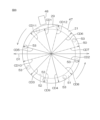
- the orientation of the SiC semiconductor wafer 21 is adjusted so that the predetermined crystal directions CD1 to CD12 of the SiC semiconductor wafer 21 are inclined with respect to the moving direction (first direction D1) of the adhesive tape 54.
- the predetermined crystal directions CD1 to CD1 of the SiC semiconductor wafer 21 are the [11-20] direction and the [1-100] direction, as well as crystal directions equivalent thereto.
- the predetermined crystal directions may be the [11-20] direction CD1, the [1-210] direction CD2, the [-2110] direction CD3, the [-1-120] direction CD4, the [-12-10] direction CD5, the [2-1-10] direction CD6, the [1-100] direction CD7, the [0-110] direction CD8, the [-1010] direction CD9, the [-1100] direction CD10, the [01-10] direction CD11, and the [10-10] direction CD12.
- the orientation flat 29 extends linearly along the m-axis direction ([1-100] direction) of the SiC single crystal, and the orientation flat 29 is detected by the position detection sensor 48. It is determined whether the crystal directions CD1 to CD12 are inclined with respect to the first direction D1 based on the position of the orientation flat 29, and the rotation of the alignment table 47 is stopped at the position where it is determined that they are inclined. More specifically, it is preferable to adjust the orientation of the SiC semiconductor wafer 21 so that the crystal directions CD1 to CD12 are inclined by ⁇ 5° or more with respect to the first direction D1.
- the predetermined crystal directions CD1 to CD12 may be, for example, directions inclined at angles of 90°, +30°, and -30° with respect to the orientation flat 29 (these are the [11-20] direction and directions CD1 to CD6 equivalent to said direction) and directions inclined at angles of 0°, +60°, and -60° (these are the [1-100] direction and directions CD7 to CD12 equivalent to said direction).
- tensioned adhesive tape 54 is transported from a supply reel 56 via a guide roller 58 to the top surface of a peeling table 55.
- the adhesive tape 54 is placed on the top surface of the peeling table 55 and becomes ready to receive a SiC semiconductor wafer 21.
- the SiC semiconductor wafer 21 in the peeling preparation position is attracted to the holding table 49 and, while maintaining the orientation of the peeling preparation position, is transported above the peeling table 55 (see the two-dot chain line in FIG. 7).
- the holding table 49 then descends and presses against the adhesive tape 54 on the peeling table 55, causing the sheet material 36 of the SiC semiconductor wafer 21 to adhere to the adhesive tape 54.
- the peeling table 55 is slid.
- the adhesive tape 54 is pulled in accordance with the sliding movement of the peeling table 55, and the sheet material 36 is peeled off together with the adhesive tape 54.
- the peeling of the sheet material 36 proceeds along a direction that avoids the crystal directions CD1 to CD12. More specifically, it is preferable that the peeling of the sheet material 36 proceeds along a direction that avoids directions that fall within a range of ⁇ 5° from the crystal directions CD1 to CD12. Meanwhile, the used adhesive tape 54 is collected by the collection reel 57 together with the sheet material 36.
- the drain electrode 20 is formed all over the second wafer main surface 23. After that, the SiC semiconductor wafer 21 is cut along the intended cutting lines 32 to cut out a plurality of semiconductor devices 1.
- the orientation of the SiC semiconductor wafer 21 is adjusted so that the crystal directions CD1 to CD12 of the SiC semiconductor wafer 21 are inclined with respect to the first direction D1, as shown in Fig. 8. Therefore, peeling of the sheet material 36 proceeds along a direction that avoids the crystal directions CD1 to CD12.
- the SiC semiconductor wafer 21 is thinned to a thickness of 50 ⁇ m or more and 350 ⁇ m or less.
- Such a relatively thin SiC semiconductor wafer 21 is prone to damage during peeling, but by adopting the peeling method of the present disclosure in which the crystal directions CD1 to CD12 are inclined relative to the pulling direction of the adhesive tape 54, damage to the SiC semiconductor wafer 21 can be effectively suppressed.
- the second wafer main surface 23 of the SiC semiconductor wafer 21 is roughened.
- a roughened SiC semiconductor wafer 21 is prone to breakage during peeling, but by employing the peeling method of the present disclosure in which the crystal directions CD1 to CD12 are inclined relative to the pulling direction of the adhesive tape 54, damage to the SiC semiconductor wafer 21 can be effectively suppressed.
- a trench gate structure is formed as the element structure 35 of the SiC semiconductor wafer 21.
- the portion where the gate trench 8 is formed becomes locally thin, and the formation of the gate trench 8 makes it easy for warping to occur. Therefore, damage is likely to occur during peeling, but by adopting the peeling method of the present disclosure in which the crystal directions CD1 to CD12 are inclined relative to the pulling direction of the adhesive tape 54, damage to the SiC semiconductor wafer 21 can be effectively suppressed.
- an interlayer insulating film 17 is formed on the first wafer main surface 22 of the SiC semiconductor wafer 21.
- the stress of this interlayer insulating film 17 can easily cause warping in the SiC semiconductor wafer 21. This can easily cause damage during peeling, but by employing the peeling method of the present disclosure in which the crystal directions CD1 to CD12 are inclined relative to the pulling direction of the adhesive tape 54, damage to the SiC semiconductor wafer 21 can be effectively suppressed.
- the detection target of the position detection sensor 48 was the orientation flat 29 of the SiC semiconductor wafer 21, but for example, as shown in FIG. 9, the orientation flat 29 may be replaced with a notch 59.
- the notch 59 may be, for example, a notch cut in a V shape along the [11-20] direction (crystal direction CD1) of the SiC semiconductor wafer 21.
- element structure 35 a MOSFET with a trench gate structure was shown as an example of element structure 35, but element structure 35 may be other element structures such as a MOSFET with a planar gate structure, an IGBT with a trench gate structure and a planar gate structure, a Schottky barrier diode, etc.
- a thinning process of the SiC semiconductor wafer 21 is shown as an example of a processing process of the second wafer main surface 23 of the SiC semiconductor wafer 21, but various processing processes may be adopted, such as a process of irradiating the second wafer main surface 23 of the SiC semiconductor wafer 21 with an electron beam, or a process of roughening the second wafer main surface 23 without thinning.
- [Appendix 1-1] a bonding step of bonding a sheet material (36) to a first main surface (3, 22) of the wafer (21) having a hexagonal close-packed structure, the first main surface (3, 22) having an element structure (7, 35) formed thereon; a processing step of processing a second main surface (4, 23) opposite to the first main surface (3, 22); and a peeling step of peeling the sheet material (36) from the first main surface (3, 22) along a direction avoiding predetermined crystal directions (CD1 to CD12) after the processing step,
- the predetermined crystal directions (CD1 to CD12) include the [11-20] direction and the [1-100] direction of the wafer (21), as well as crystal directions (CD1 to CD12) equivalent thereto.
- the sheet material (36) is peeled off along a direction that avoids the [11-20] and [1-100] directions of the wafer (21) and their equivalent crystal directions (CD1 to CD12).
- the wafer (21) is likely to be damaged along the crystal directions (CD1 to CD12). Therefore, by peeling the sheet material (36) off along a direction that avoids the crystal directions (CD1 to CD12), damage to the wafer (21) during peeling of the sheet material (36) can be suppressed.
- Appendix 1-2 The method for manufacturing a semiconductor device (1) described in Appendix 1-1, wherein in the peeling step, the sheet material (36) is peeled off along a direction avoiding a direction falling within a range of ⁇ 5° from the specified crystal direction (CD1 to CD12).
- Appendix 1-3 The method for manufacturing a semiconductor device (1) according to Appendix 1-1 or Appendix 1-2, wherein the processing step includes a step of thinning the wafer (21) from the second main surface (4, 23) until the wafer has a thickness of 50 ⁇ m or more and 350 ⁇ m or less.
- Such a relatively thin wafer (21) is prone to damage during peeling, but by adopting the peeling method disclosed herein, damage to the wafer (21) can be effectively suppressed.
- Roughened wafers (21) are prone to damage during peeling, but by adopting the peeling method disclosed herein, damage to the wafer (21) can be effectively prevented.
- Appendix 1-6 The method for manufacturing a semiconductor device (1) according to any one of Appendix 1-1 to Appendix 1-5, wherein the element structure (7, 35) includes a trench element structure (7, 35) formed on the first main surface (3, 22) of the wafer (21).
- Appendix 1-7 The method for manufacturing a semiconductor device (1) according to appendix 1-6, wherein the depth of the trench element structure (7, 35) is 1 ⁇ m or more.
- the wafer (21) includes a first semiconductor region (13) of a first conductivity type formed in a surface layer portion of the first main surface (3, 22), The method for manufacturing a semiconductor device (1) described in Appendix 1-6 or Appendix 1-7, wherein the trench element structure (7, 35) includes a gate trench (8) formed in the first main surface (3, 22), a gate electrode (10) embedded in the gate trench (8) via a gate insulating film (9), and a second semiconductor region (14) of a first conductivity type and a third semiconductor region (11) of a second conductivity type formed in this order from the first main surface (3, 22) in a depth direction of the gate trench (8).
- Appendix 1-9 A method for manufacturing a semiconductor device (1) according to any one of Appendix 1-1 to Appendix 1-8, comprising forming an insulating film (17) on the first main surface (3, 22) of the wafer (21) so as to cover the element structure (7, 35).
- the stress of the insulating film (17) can easily cause warping in the wafer (21). This can easily lead to damage during peeling, but by employing the peeling method disclosed herein, damage to the wafer (21) can be effectively prevented.
- Appendix 1-10 The method for manufacturing a semiconductor device (1) according to appendix 1-9, wherein the insulating film (17) includes an interlayer insulating film (17) having a thickness of 0.2 ⁇ m or more and 2.0 ⁇ m or less.
- [Appendix 1-11] The method for manufacturing a semiconductor device (1) according to any one of Appendix 1-1 to Appendix 1-10, wherein the wafer (21) includes an orientation flat (29) extending linearly along a direction perpendicular to the [11-20] direction of the wafer (21), or a notch (59) cut in a V-shape along the [11-20] direction of the wafer (21).
- the orientation of the wafer (21) is adjusted so that the [11-20] and [1-100] directions of the wafer (21) and their equivalent crystal directions (CD1 to CD12) are inclined with respect to the first direction (D1). Therefore, the peeling of the sheet material (36) proceeds along a direction that avoids the crystal directions (CD1 to CD12). As a result, damage to the wafer (21) during the peeling of the sheet material (36) can be suppressed.
- the wafer supply unit (39) includes a mechanism (47, 48) for adjusting the orientation of the wafer (21) so that the predetermined crystal direction (CD1 to CD12) is inclined by ⁇ 5° or more with respect to the first direction (D1).
- the sheet material peeling device (37) used in the manufacturing method of the semiconductor device (1) according to appendix 1-11, The sheet material peeling device (37) described in Appendix 1-12 or Appendix 1-13, wherein the wafer supply unit (39) includes a sensor (48) that detects the orientation flat (29) or the notch (59) of the wafer (21), and an alignment table (47) that rotatably holds the wafer (21).
Landscapes
- Crystals, And After-Treatments Of Crystals (AREA)
Abstract
半導体装置の製造方法は、六方最密充填構造を有するウエハであって、素子構造が形成されたウエハの第1主面にシート材を貼付する貼付工程と、第1主面の反対側の第2主面を加工する加工工程と、加工工程の後、所定の結晶方向を避けた方向に沿ってシート材を第1主面から剥離する剥離工程とを含み、所定の結晶方向は、ウエハの[11-20]方向および[1-100]方向、ならびにこれらと等価な結晶方向を含む。
Description
本出願は、2022年12月15日に日本国特許庁に提出された特願2022-200641号に対応しており、この出願の全開示はここに引用により組み込まれるものとする。
本開示は、半導体装置の製造方法、および当該製造方法に使用可能なシート材剥離装置に関する。
たとえば、特許文献1は、SiC半導体基板およびSiCエピタキシャル層を含む積層構造を有し、SiCエピタキシャル層によって形成された第1主面(素子形成面)、ならびに、SiC半導体基板およびSiCエピタキシャル層によって形成された側面を有するSiC半導体層と、側面においてSiCエピタキシャル層から間隔を空けてSiC半導体基板からなる部分に形成され、SiC半導体基板とは異なる性質に改質された改質ラインとを含む、SiC半導体装置を開示している。
シート材の剥離時におけるウエハの破損を抑制することができる、半導体装置の製造方法、および当該製造方法に使用可能なシート材剥離装置を提供する。
本開示の一実施形態に係る半導体装置の製造方法は、六方最密充填構造を有するウエハであって、素子構造が形成された前記ウエハの第1主面にシート材を貼付する貼付工程と、前記第1主面の反対側の第2主面を加工する加工工程と、前記加工工程の後、所定の結晶方向を避けた方向に沿って前記シート材を前記第1主面から剥離する剥離工程とを含み、前記所定の結晶方向は、前記ウエハの[11-20]方向および[1-100]方向、ならびにこれらと等価な結晶方向を含む。
本開示の一実施形態に係るシート材剥離装置は、前記半導体装置の製造方法に使用されるシート材剥離装置であって、前記シート材が貼付された前記ウエハをセット可能であり、粘着テープを第1方向に沿って移動させることにより、セットされた前記ウエハから前記シート材を前記粘着テープにより剥離する剥離ユニットと、前記剥離ユニット上に前記粘着テープを供給するテープ供給ユニットと、使用済みの前記粘着テープを回収するテープ回収ユニットと、前記所定の結晶方向が前記第1方向に対して傾斜した方向となるように前記ウエハの向きを調整し、前記剥離ユニット上に前記ウエハを供給するウエハ供給ユニットとを含む。
本開示の一実施形態に係る半導体装置の製造方法によれば、シート材の剥離時におけるウエハの破損を抑制することができる。
以下では、本開示の実施形態を、添付図面を参照して詳細に説明する。
[SiC単結晶の結晶構造]
本開示の実施形態では、六方晶(六方最密構造)からなるSiC(炭化シリコン)単結晶が適用される。六方晶からなるSiC単結晶は、原子配列の周期に応じて、2H(Hexagonal)-SiC単結晶、4H-SiC単結晶および6H-SiC単結晶を含む複数種のポリタイプを有している。本開示の実施形態では、4H-SiC単結晶が適用された例について説明するが、他のポリタイプを本開示から除外するものではない。
本開示の実施形態では、六方晶(六方最密構造)からなるSiC(炭化シリコン)単結晶が適用される。六方晶からなるSiC単結晶は、原子配列の周期に応じて、2H(Hexagonal)-SiC単結晶、4H-SiC単結晶および6H-SiC単結晶を含む複数種のポリタイプを有している。本開示の実施形態では、4H-SiC単結晶が適用された例について説明するが、他のポリタイプを本開示から除外するものではない。
以下、4H-SiC単結晶の結晶構造について説明する。図1は、本開示の実施形態に適用される4H-SiC単結晶の単位セル(以下、単に「単位セル」という。)を示す図である。図2は、図1に示す単位セルのシリコン面を示す平面図である。
図1および図2を参照して、単位セルは、1つのSi原子に対して4つのC原子が四面体配列(正四面体配列)の関係で結合された四面体構造を含む。単位セルは、四面体構造が4周期積層された原子配列を有している。単位セルは、正六角形のシリコン面、正六角形のカーボン面、ならびに、シリコン面およびカーボン面を接続する6つの側面を有する六角柱構造を有している。
シリコン面は、Si原子によって終端された終端面である。シリコン面では、正六角形の6つの頂点に1つのSi原子がそれぞれ位置し、正六角形の中心に1つのSi原子が位置している。
カーボン面は、C原子によって終端された終端面である。カーボン面では、正六角形の6つの頂点に1つのC原子がそれぞれ位置し、正六角形の中心に1つのC原子が位置している。
単位セルの結晶面は、a1軸、a2軸、a3軸およびc軸を含む4つの座標軸(a1,a2,a3,c)によって定義される。4つの座標軸のうちのa3の値は、-(a1+a2)の値をとる。以下、六方晶の終端面の一例としてのシリコン面を基準にして、4H-SiC単結晶の結晶面について説明する。
a1軸、a2軸およびa3軸は、シリコン面をc軸から見た平面視において、中心に位置するSi原子を基準に、最近接するSi原子の配列方向(以下、単に「最近接原子方向」という。)に沿ってそれぞれ設定されている。a1軸、a2軸およびa3軸は、それぞれ、Si原子の配列に倣って120°ずつ角度をずらして設定されている。
c軸は、中心に位置するSi原子を基準に、シリコン面の法線方向に設定されている。シリコン面は、(0001)面である。カーボン面は、(000-1)面である。
六角柱の側面は、シリコン面をc軸から見た平面視において、最近接原子方向に沿う6つの結晶面を含む。六角柱の側面は、より具体的には、シリコン面をc軸から見た平面視において、最近接する2つのSi原子をそれぞれ含む6つの結晶面を含む。
六角柱の側面は、シリコン面をc軸から見た平面視において、a1軸の先端から時計回りに(1-100)面、(0-110)面、(-1010)面、(-1100)面、(01-10)面および(10-10)面を含む。
六角柱の対角線に沿う対角面は、シリコン面をc軸から見た平面視において、最近接原子方向に交差する交差方向に沿う6つの結晶面を含む。六角柱の対角面は、より具体的には、シリコン面をc軸から見た平面視において、最近接しない2つのSi原子をそれぞれ含む6つの結晶面を含む。中心に位置するSi原子を基準に見たとき、最近接原子方向の交差方向は、最近接原子方向に直交する直交方向となる。
六角柱の対角面は、シリコン面をc軸から見た平面視において、(11-20)面、(1-210)面、(-2110)面、(-1-120)面、(-12-10)面および(2-1-10)面を含む。
単位セルの結晶方向は、結晶面の法線方向によって定義される。(1-100)面の法線方向は[1-100]方向である。(0-110)面の法線方向は[0-110]方向である。(-1010)面の法線方向は[-1010]方向である。(-1100)面の法線方向は[-1100]方向である。(01-10)面の法線方向は[01-10]方向である。(10-10)面の法線方向は[10-10]方向である。
(11-20)面の法線方向は[11-20]方向である。(1-210)面の法線方向は[1-210]方向である。(-2110)面の法線方向は[-2110]方向である。(-1-120)面の法線方向は[-1-120]方向である。(-12-10)面の法線方向は[-12-10]方向である。(2-1-10)面の法線方向は[2-1-10]方向である。
六方晶は6回対称であり、60°毎に等価な結晶面および等価な結晶方向が存在している。たとえば、(1-100)面、(0-110)面、(-1010)面、(-1100)面、(01-10)面および(10-10)面は、等価な結晶面を形成している。
また、[1-100]方向、[0-110]方向、[-1010]方向、[-1100]方向、[01-10]方向および[10-10]方向は、等価な結晶方向を形成している。また、[11-20]方向、[1-210]方向、[-2110]方向、[-1-120]方向、[-12-10]方向および[2-1-10]方向は、等価な結晶方向を形成している。
c軸は、[0001]方向([000-1]方向)である。a1軸は、[2-1-10]方向([-2110]方向)である。a2軸は、[-12-10]方向([1-210]方向)である。a3軸は、[-1-120]方向([11-20]方向)である。
(0001)面および(000-1)面は、c面と総称される。[0001]方向および[000-1]方向は、c軸方向と総称される。(11-20)面および(-1-120)面は、a面と総称される。[11-20]方向および[-1-120]方向は、a軸方向と総称される。(1-100)面および(-1100)面は、m面と総称される。[1-100]方向および[-1100]方向は、m軸方向と総称される。
[半導体装置1の構造]
図3は、本開示の一実施形態に係る半導体装置1の模式的な断面図である。
図3は、本開示の一実施形態に係る半導体装置1の模式的な断面図である。
半導体装置1は、この形態ではSiC半導体装置であり、SiC半導体層2を含む。SiC半導体層2は、六方晶からなるSiC単結晶の一例としての4H-SiC単結晶を含む。SiC半導体層2は、直方体形状のチップ状に形成されている。
SiC半導体層2は、一方側の第1主面3および他方側の第2主面4を有している。第1主面3および第2主面4は、それらの法線方向Zから見た平面視(以下、単に「平面視」という。)において四角形状(この形態では正方形状)に形成されている。
第1主面3は、半導体素子が形成された素子形成面である。SiC半導体層2の第2主面4は、研削痕を有する研削面からなる。
SiC半導体層2の厚さTLは、50μm以上350μm以下であってもよい。厚さTLは、80μm以上350μm以下、100μm以上350μm以下、150μm以上350μm以下、50μm以上300μm以下、80μm以上300μm以下、100μm以上300μm以下、150μm以上300μm以下、50μm以上250μm以下、80μm以上250μm以下、100μm以上250μm以下、150μm以上250μm以下であってもよい。厚さTLは、50μm以350μm以下であることが好ましく、50μm以上300μm以下であることがさらに好ましい。
第1主面3および第2主面4は、この形態では、SiC単結晶のc面に面している。第1主面3は、(0001)面(シリコン面)に面している。第2主面4は、SiC単結晶の(000-1)面(カーボン面)に面している。
第1主面3および第2主面4は、SiC単結晶のc面に対して[11-20]方向に10°以下の角度で傾斜したオフ角θを有している。法線方向Zは、SiC単結晶のc軸([0001]方向)に対してオフ角θ分だけ傾斜している。
オフ角θは、0°以上5.0°以下であってもよい。オフ角θは、0°以上1.0°以下、1.0°以上1.5°以下、1.5°以上2.0°以下、2.0°以上2.5°以下、2.5°以上3.0°以下、3.0°以上3.5°以下、3.5°以上4.0°以下、4.0°以上4.5°以下または4.5°以上5.0°以下の角度の範囲に設定されてもよい。オフ角θは、0°を超えていることが好ましい。オフ角θは、4.0°未満であってもよい。
オフ角θは、3.0°以上4.5°以下の角度の範囲に設定されていてもよい。この場合、オフ角θは、3.0°以上3.5°以下または3.5°以上4.0°以下の角度の範囲に設定されていることが好ましい。
オフ角θは、1.5°以上3.0°以下の角度の範囲に設定されていてもよい。この場合、オフ角θは、1.5°以上2.0°以下または2.0°以上2.5°以下の角度の範囲に設定されていることが好ましい。
第1主面3は、デバイス形成面である。第1主面3は、非実装面である。第2主面4は、実装面である。半導体装置1が接続対象物に実装される場合、SiC半導体層2は、第2主面4を対向させた姿勢で接続対象物に実装される。接続対象物としては、電子部品、リードフレーム、回路基板等が例示される。
第2主面4は、粗面化された粗面化面からなる。第2主面4は、不規則に形成された凹凸(Unevenness)によって粗面化されている。第2主面4の全域が粗面化されていることが好ましい。第2主面4は、研削痕(より具体的にはライン状に延びる研削痕)を有さない粗面化面からなることが特に好ましい。第2主面4は、より具体的には、Si単結晶からなる結晶面である。したがって、第2主面4は、Si単結晶が粗面化された結晶粗面化面からなる。
第2主面4の算術平均粗さRaは、5nm以上であってもよい。第2主面4の算術平均粗さRaは、5nm以上1000nm以下、5nm以上800nm以下、5nm以上600nm以下、5nm以上400nm以下、5nm以上100nm以下であってもよい。第2主面4の算術平均粗さRaは、5nm以上100nm以下であることが好ましい。
SiC半導体層2は、この形態では、n+型のSiC半導体基板5およびn型のSiCエピタキシャル層6を含む積層構造を有している。SiC半導体基板5によって、SiC半導体層2の第2主面4が形成されている。SiCエピタキシャル層6によって、SiC半導体層2の第1主面3が形成されている。なお、図3では、各構成要素の明瞭化のために、SiC半導体基板5がSiCエピタキシャル層6よりも薄く示されているが、SiC半導体基板5およびSiCエピタキシャル層6の厚さの比率は適宜変更することができる。
SiCエピタキシャル層6のn型不純物濃度は、SiC半導体基板5のn型不純物濃度以下である。SiCエピタキシャル層6のn型不純物濃度は、より具体的には、SiC半導体基板5のn型不純物濃度未満である。SiC半導体基板5のn型不純物濃度は、1.0×1018cm-3以上1.0×1021cm-3以下であってもよい。SiCエピタキシャル層6のn型不純物濃度は、1.0×1015cm-3以上1.0×1018cm-3以下であってもよい。
SiC半導体基板5の厚さTSは、40μm以上150μm以下であってもよい。厚さTSは、40μm以上50μm以下、50μm以上60μm以下、60μm以上70μm以下、70μm以上80μm以下、80μm以上90μm以下、90μm以上100μm以下、100μm以上110μm以下、110μm以上120μm以下、120μm以上130μm以下、130μm以上140μm以下または140μm以上150μm以下であってもよい。厚さTSは、40μm以上130μm以下であることが好ましい。SiC半導体基板5の薄化によって、電流経路の短縮による抵抗値の低減を図ることができる。
SiCエピタキシャル層6の厚さTEは、1μm以上50μm以下であってもよい。厚さTEは、1μm以上5μm以下、5μm以上10μm以下、10μm以上15μm以下、15μm以上20μm以下、20μm以上25μm以下、25μm以上30μm以下、30μm以上35μm以下、35μm以上40μm以下、40μm以上45μm以下または45μm以上50μm以下であってもよい。厚さTEは、5μm以上15μm以下であることが好ましい。
半導体装置1は、素子構造の一例としてトレンチゲート構造のMOSFETを含む。SiCエピタキシャル層6の第1主面3の表層部には、複数の単位セル7を区画するゲートトレンチ8が形成されている。複数のゲートトレンチ8は、a軸方向に沿って延びるストライプ状に形成されていてもよい。
各ゲートトレンチ8の底部は、SiCエピタキシャル層6の厚さ方向途中部に位置している。各ゲートトレンチ8の側面と底部とが交わるエッジ部は、各ゲートトレンチ8の外方へ向かって湾曲する形状に形成されており、各ゲートトレンチ8は断面視U字状に形成されている。各ゲートトレンチ8のエッジ部が湾曲状であれば、当該エッジ部に集中する電界を緩和できる。ゲートトレンチ8の深さは、たとえば、1μm以上であってもよい。
各ゲートトレンチ8には、ゲート絶縁膜9を介してゲート電極10が埋め込まれている。ゲート電極10は、SiCエピタキシャル層6の第1主面3と面一な表面を有している。ゲート絶縁膜9は、たとえば、シリコン酸化膜、シリコン窒化膜、シリコン酸窒化膜、ハフニウム酸化膜、アルミナ膜、タンタル酸化膜等からなっていてもよい。また、ゲート電極10は、たとえば、不純物を注入して低抵抗化したポリシリコンからなっていてもよい。互いに隣り合うゲートトレンチ8間の領域に、単位セル7を構成するp型のボディ領域11が形成されている。
ボディ領域11の底部は、SiCエピタキシャル層6の厚さ方向に関して、SiCエピタキシャル層6の第1主面3とゲートトレンチ8の底部との間に位置している。SiCエピタキシャル層6の第1主面3に沿う横方向において、ボディ領域11の端部は、ゲートトレンチ8の一部を形成している。つまり、ボディ領域11は、ゲート絶縁膜9を挟んでゲート電極10に対向している。
この形態では、SiC半導体基板5がn+型のドレイン領域12であり、ボディ領域11とドレイン領域12との間の領域がn-型のドリフト領域13である。
ボディ領域11の内方領域には、n型のソース領域14が形成されている。ソース領域14は、SiCエピタキシャル層6の厚さ方向に関して、ボディ領域11よりも浅く形成されている。SiCエピタキシャル層6の第1主面3に沿う横方向において、ソース領域14の端部は、ゲートトレンチ8の一部を形成している。つまり、ソース領域14は、ゲート絶縁膜9を挟んでゲート電極10に対向している。
SiCエピタキシャル層6の厚さ方向に関して、ゲートトレンチ8の側面に沿うソース領域14の下端とボディ領域11の下端との間の領域がp型のチャネル領域15である。ソース領域14を貫通するようにp+型のボディコンタクト領域16が形成されている。
ボディコンタクト領域16は、ソース領域14を貫通して、ソース領域14とボディ領域11との境界を横切るように形成されている。ボディコンタクト領域16は、ボディ領域11よりも高い不純物濃度を有している。
SiCエピタキシャル層6上には、ゲート電極10を覆う層間絶縁膜17が形成されている。層間絶縁膜17の厚さは、たとえば、0.2μm以上2.0μm以下であってもよい。層間絶縁膜17には、ソース領域14の一部およびボディコンタクト領域16を選択的に露出させるコンタクト孔18が形成されている。層間絶縁膜17上には、ソース電極19が形成されている。ソース電極19は、たとえば、純Al層(純度が99%以上のAl層)、Cu層(純度が99%以上のCu層)、AlCu合金層、AlSiCu合金層およびAlSi合金層のうちの少なくとも1種を含んでいてもよい。
ソース電極19は、コンタクト孔18内において、ボディ領域11、ソース領域14の一部およびボディコンタクト領域16との間でオーミックコンタクトを形成している。一方、SiC半導体基板5の第2主面4には、ドレイン電極20が形成されている。ドレイン電極20は、ドレイン領域12との間でオーミックコンタクトを形成している。ドレイン電極20は、たとえば、純Al層(純度が99%以上のAl層)、Cu層(純度が99%以上のCu層)、AlCu合金層、AlSiCu合金層およびAlSi合金層のうちの少なくとも1種を含んでいてもよい。
[半導体装置1の製造方法]
図4は、半導体装置1の製造に使用されるSiC半導体ウエハ21を示す斜視図である。図5A~図5Eは、半導体装置1の製造工程の一部を工程順に示す図である。
図4は、半導体装置1の製造に使用されるSiC半導体ウエハ21を示す斜視図である。図5A~図5Eは、半導体装置1の製造工程の一部を工程順に示す図である。
SiC半導体ウエハ21は、SiC半導体基板5のベースとなる部材である。SiC半導体ウエハ21は、六方晶からなるSiC単結晶の一例としての4H-SiC単結晶を含む。SiC半導体ウエハ21は、この形態では、SiC半導体基板5のn型不純物濃度に対応したn型不純物濃度を有している。
SiC半導体ウエハ21は板状または盤状に形成されている。SiC半導体ウエハ21は、円盤状に形成されていてもよい。SiC半導体ウエハ21は、一方側の第1ウエハ主面22、他方側の第2ウエハ主面23、ならびに、第1ウエハ主面22および第2ウエハ主面23を接続するウエハ側面24を有している。
SiC半導体ウエハ21の厚さTWは、SiC半導体基板5の厚さTS(図3参照)を超えている(TS<TW)。SiC半導体ウエハ21の厚さTWは、研削によってSiC半導体基板5の厚さTSに合わせ込まれる。
厚さTWは、150μmを超えて750μm以下であってもよい。厚さTWは、150μmを超えて300μm以下、300μm以上450μm以下、450μm以上600μm以下または600μm以上750μm以下であってもよい。SiC半導体ウエハ21の研削時間を鑑みると、厚さTWは、150μmを超えて500μm以下であることが好ましい。厚さTWは、典型的には、300μm以上450μm以下である。
第1ウエハ主面22および第2ウエハ主面23は、この形態では、SiC単結晶のc面に面している。第1ウエハ主面22は、(0001)面(シリコン面)に面している。第2ウエハ主面23は、SiC単結晶の(000-1)面(カーボン面)に面している。
第1ウエハ主面22および第2ウエハ主面23は、SiC単結晶のc面に対して[11-20]方向に10°以下の角度で傾斜したオフ角θを有している。第1ウエハ主面22の法線方向Zは、SiC単結晶のc軸([0001]方向)に対してオフ角θ分だけ傾斜している。
オフ角θは、0°以上5.0°以下であってもよい。オフ角θは、0°以上1.0°以下、1.0°以上1.5°以下、1.5°以上2.0°以下、2.0°以上2.5°以下、2.5°以上3.0°以下、3.0°以上3.5°以下、3.5°以上4.0°以下、4.0°以上4.5°以下または4.5°以上5.0°以下の角度の範囲に設定されてもよい。オフ角θは、0°を超えていることが好ましい。オフ角θは、4.0°未満であってもよい。
オフ角θは、3.0°以上4.5°以下の角度の範囲に設定されていてもよい。この場合、オフ角θは、3.0°以上3.5°以下または3.5°以上4.0°以下の角度の範囲に設定されていることが好ましい。
オフ角θは、1.5°以上3.0°以下の角度の範囲に設定されていてもよい。この場合、オフ角θは、1.5°以上2.0°以下または2.0°以上2.5°以下の角度の範囲に設定されていることが好ましい。
SiC半導体ウエハ21は、第1ウエハ主面22およびウエハ側面24を接続する第1ウエハ角部25、ならびに、第2ウエハ主面23およびウエハ側面24を接続する第2ウエハ角部26を含む。第1ウエハ角部25は、第1ウエハ主面22からウエハ側面24に向かって下り傾斜した第1面取り部27を有している。第2ウエハ角部26は、第2ウエハ主面23からウエハ側面24に向かって下り傾斜した第2面取り部28を有している。
第1面取り部27は、凸湾曲状に形成されていてもよい。第2面取り部28は、凸湾曲状に形成されていてもよい。第1面取り部27および第2面取り部28は、SiC半導体ウエハ21のクラックを抑制する。
SiC半導体ウエハ21のウエハ側面24には、SiC単結晶の結晶方位を示す目印の一例として1つのオリエンテーションフラット29が形成されている。オリエンテーションフラット29は、SiC半導体ウエハ21のウエハ側面24に形成された切欠部である。オリエンテーションフラット29は、この形態では、SiC単結晶のm軸方向([1-100]方向)に沿って直線状に延びている。
SiC半導体ウエハ21のウエハ側面24には、結晶方位を示す複数(たとえば2つ)のオリエンテーションフラット29が形成されていてもよい。複数(たとえば2つ)のオリエンテーションフラット29は、第1オリエンテーションフラットおよび第2オリエンテーションフラットを含んでいてもよい。
第1オリエンテーションフラットは、SiC単結晶のm軸方向([1-100]方向)に沿って直線状に延びる切欠部であってもよい。第2オリエンテーションフラットは、SiC単結晶のa軸方向([11-20]方向)に沿って直線状に延びる切欠部であってもよい。
SiC半導体ウエハ21の第1ウエハ主面22には、半導体装置1にそれぞれ対応した複数の装置形成領域30が設定される。複数の装置形成領域30は、m軸方向([1-100]方向)およびa軸方向([11-20]方向)に間隔を空けて行列状の配列で設定される。
各装置形成領域30は、SiC単結晶の結晶方位に沿った4つの辺31A,31B,31C,31Dを有している。4つの辺31A~31Dは、SiC半導体層2の4つの側面にそれぞれ対応している。4つの辺31A~31Dは、m軸方向([1-100]方向)に沿う2つの辺31B,31Dおよびa軸方向([11-20]方向)に沿う2つの辺31A,31Cを含む。
複数の装置形成領域30は、m軸方向([1-100]方向)およびa軸方向([11-20]方向)に沿って延びる格子状の切断予定ライン32によってそれぞれ区画されている。切断予定ライン32は、複数の第1切断予定ライン33および複数の第2切断予定ライン34を含む。
複数の第1切断予定ライン33は、a軸方向([11-20]方向)に沿ってそれぞれ延びている。複数の第2切断予定ライン34は、m軸方向([1-100]方向)に沿ってそれぞれ延びている。
半導体装置1の製造工程では、図5Aを参照して、複数の装置形成領域30に所定の素子構造35(前述のトレンチゲート構造のMOSFETの各単位セル7)が作り込まれる。
次に、図5Bを参照して、素子構造35を被覆するように、SiC半導体ウエハ21の第1ウエハ主面22に層間絶縁膜17が形成される。層間絶縁膜17は、たとえば、CVD法等によって第1ウエハ主面22の全面に形成される。層間絶縁膜17の形成後、素子構造35に電気的に接続される第1ウエハ主面22側の配線構造(図示せず)が形成される。当該配線構造は、前述のソース電極19等を含んでいてもよい。
次に、図5Cを参照して、シート材36が、SiC半導体ウエハ21の第1ウエハ主面22に貼付される。シート材36は、たとえば、SiC半導体ウエハ21を研削により薄化する際に素子構造35を保護するためのシートであり、保護シート、保護テープ等と称されてもよい。シート材36としては、たとえば、公知の裏面研削用の保護テープを使用することができる。また、シート材36は、たとえば、公知のテープ貼付装置によりSiC半導体ウエハ21に貼付することができる。
次に、図5Dを参照して、SiC半導体ウエハ21の第2ウエハ主面23が研削される。SiC半導体ウエハ21の第2ウエハ主面23は、CMP(Chemical Mechanical Polishing)法によって研削されてもよい。これにより、SiC半導体ウエハ21が所望の厚さまで薄化される。この実施形態では、SiC半導体ウエハ21は、50μm以上350μm以下の厚さになるまで薄化される。この際、薄化の最終仕上げ工程として、SiC半導体ウエハ21の第2ウエハ主面23が粗面化されてもよい。第2ウエハ主面23は、エッチング法によって粗面化されることが好ましい。第2ウエハ主面23は、5nm以上の算術平均粗さRaになるまで粗面化されてもよい。第2ウエハ主面23は、算術平均粗さRaが、5nm以上100nm以下になるまで粗面化されることが好ましい。
次の工程は、シート材36の剥離工程である。シート材36の剥離には、本開示の一実施形態に係るシート材剥離装置37が使用される。図6は、本開示の一実施形態に係るシート材剥離装置37の模式的な平面図である。図7は、本開示の一実施形態に係るシート材剥離装置37の模式的な断面図である。
図6および図7を参照して、シート材剥離装置37は、ウエハ搬送ユニット38と、ウエハ供給ユニット39と、剥離ユニット40と、テープ供給ユニット41と、テープ回収ユニット42とを含む。
ウエハ搬送ユニット38は、シート材36が貼付されたSiC半導体ウエハ21をウエハ供給ユニット39に搬送する。ウエハ搬送ユニット38は、たとえば、アーム43を有する搬送ロボット44を含んでいてもよい。シート材36が貼付されたSiC半導体ウエハ21は、複数枚を一括にしてウエハ搬送ユニット38の基板収容部45にまとめて収容される。ウエハ搬送ユニット38は、アーム43の先端部に形成された吸着ハンド46によって基板収容部45のSiC半導体ウエハ21を1枚ずつ吸着し、ウエハ供給ユニット39に搬送する。
ウエハ供給ユニット39は、SiC半導体ウエハ21の向きを調整する機能を有している。ウエハ供給ユニット39は、SiC半導体ウエハ21の向きの調整後、SiC半導体ウエハ21を剥離ユニット40上に供給する。
ウエハ供給ユニット39は、アライメントテーブル47と、位置検出センサ48と、保持テーブル49とを含む。
アライメントテーブル47は、図6に示すように、たとえば平面視円形状に形成されている。アライメントテーブル47は、SiC半導体ウエハ21の周縁部50を支持する環状の枠部51と、枠部51に取り囲まれた中空部52とを含む円環状に形成されている。枠部51には、アライメントテーブル47の周方向に沿って複数の吸引孔53が形成されている。吸引孔53からアライメントテーブル47の内部に向かう吸引によって、SiC半導体ウエハ21の周縁部50がアライメントテーブル47に吸着固定される。アライメントテーブル47は、シート材剥離装置37において、水平方向に回転自在に設けられている。したがって、吸着固定されたSiC半導体ウエハ21をアライメントテーブル47の回転力により回転させ、SiC半導体ウエハ21の向きを調整することができる。
図6を参照して、位置検出センサ48は、アライメントテーブル47の周囲に配置されている。位置検出センサ48は、たとえば、光学センサを含み、SiC半導体ウエハ21のオリエンテーションフラット29を検出する。
保持テーブル49は、たとえば、下面に複数の吸引孔(図示せず)を有しており、当該吸引孔からの吸引によってSiC半導体ウエハ21を吸着することができる。保持テーブル49は、水平方向に移動可能であり、吸着したSiC半導体ウエハ21を剥離ユニット40上に搬送する。
剥離ユニット40は、SiC半導体ウエハ21に貼付されたシート材36に粘着テープ54を密着させ、粘着テープ54と一体的にシート材36を剥離する。剥離ユニット40は、たとえば、SiC半導体ウエハ21をセット可能な剥離テーブル55を含む。剥離テーブル55は、たとえば、水平方向に平行な第1方向D1に沿って延びる一対のレール(図示せず)に支持されており、第1方向D1に沿ってスライド自在に設けられている。剥離テーブル55上の粘着テープ54は、剥離テーブル55が第1方向D1に沿ってスライドすることによって、そのスライド移動に追随して、第1方向D1に沿って相対的に移動する。第1方向D1は、粘着テープ54が移動する方向であり、たとえば、粘着テープ54の移動方向、粘着テープ54の進行方向、粘着テープ54の引っ張り方向と称されてもよい。
テープ供給ユニット41およびテープ回収ユニット42は、粘着テープ54を介して互いに結合されている。粘着テープ54は、テープ供給ユニット41の供給リール56に巻回されている。粘着テープ54は、剥離ユニット40を介してテープ回収ユニット42の回収リール57に向かって第1方向D1に沿って搬送され、回収リール57で巻き取られる。供給リール56と回収リール57との間には、ガイドローラ58やモータ(図示せず)等が設置されている。供給リール56から回収リール57に向かって搬送される粘着テープ54には、ガイドローラ58のテンションやモータの動力等により適宜の張力が付与される。
図5E、図6および図7を参照して、SiC半導体ウエハ21からシート材36を剥離するには、搬送ユニットの吸着ハンド46の吸着によって基板収容部45から1枚のSiC半導体ウエハ21が取り出され、アライメントテーブル47に搬送される。アライメントテーブル47では、吸引孔53からの吸引によってSiC半導体ウエハ21を固定した状態で、SiC半導体ウエハ21の向きが調整される。
より具体的には、図8を参照して、SiC半導体ウエハ21の所定の結晶方向CD1~CD12が、粘着テープ54の移動方向(第1方向D1)に対して傾斜した方向となるようにSiC半導体ウエハ21の向きが調整される。図8を参照して、この実施形態では、SiC半導体ウエハ21の所定の結晶方向CD1~CD1は、[11-20]方向および[1-100]方向、ならびにこれらと等価な結晶方向である。より具体的には、所定の結晶方向は、[11-20]方向CD1、[1-210]方向CD2、[-2110]方向CD3、[-1-120]方向CD4、[-12-10]方向CD5、[2-1-10]方向CD6、[1-100]方向CD7、[0-110]方向CD8、[-1010]方向CD9、[-1100]方向CD10、[01-10]方向CD11および[10-10]方向CD12であってもよい。
この実施形態では、オリエンテーションフラット29がSiC単結晶のm軸方向([1-100]方向)に沿って直線状に延びているので、オリエンテーションフラット29を位置検出センサ48で検出する。オリエンテーションフラット29の位置を基準にして結晶方向CD1~CD12が第1方向D1に対して傾斜しているかどうか判別し、傾斜していると判別されている位置においてアライメントテーブル47の回転を停止する。より具体的には、結晶方向CD1~CD12が第1方向D1に対して、±5°以上傾斜した方向となるようにSiC半導体ウエハ21の向きを調整することが好ましい。
この位置は、SiC半導体ウエハ21の剥離準備位置と称されてもよい。図8に示すように、所定の結晶方向CD1~CD12は、たとえば、オリエンテーションフラット29に対して、90°、+30°、-30°の角度で傾斜した方向(以上、[11-20]方向および当該方向に等価な方向CD1~CD6)と、0°、+60°、-60°の角度で傾斜した方向(以上、[1-100]方向および当該方向に等価な方向CD7~CD12)であってもよい。
シート材剥離装置37の剥離セクション側では、供給リール56からガイドローラ58を介して張力が付与された粘着テープ54が、剥離テーブル55の上面に搬送される。粘着テープ54は、剥離テーブル55の上面に配置され、SiC半導体ウエハ21の受け入れ準備状態となる。
次に、剥離準備位置にあるSiC半導体ウエハ21が保持テーブル49で吸着され、剥離準備位置の向きを保持したまま、剥離テーブル55の上方に搬送される(図7の二点鎖線参照)。そのまま保持テーブル49が下降し、剥離テーブル55上の粘着テープ54に保持テーブル49を押し付けることによって、SiC半導体ウエハ21のシート材36が粘着テープ54に密着する。
そして、保持テーブル49の押圧によりSiC半導体ウエハ21が固定された状態で、剥離テーブル55をスライド移動させる。これにより、図5Eに示すように、剥離テーブル55のスライド移動に追随して粘着テープ54が引っ張られ、シート材36が粘着テープ54と一体的に剥離される。この実施形態では、SiC半導体ウエハ21の結晶方向CD1~CD12(図8参照)が第1方向D1に対して傾斜しているので、結晶方向CD1~CD12を避けた方向に沿ってシート材36の剥離が進行する。より具体的には、結晶方向CD1~CD12から±5°の範囲に収まる方向を避けた方向に沿ってシート材36の剥離が進行することが好ましい。一方、使用済みの粘着テープ54は、シート材36と共に回収リール57で回収される。
次に、第2ウエハ主面23の全域に一括してドレイン電極20が形成される。その後は、切断予定ライン32に沿ってSiC半導体ウエハ21を切断することによって、複数の半導体装置1が切り出される。
[半導体装置1の製造方法による効果]
以上、本開示の一実施形態によれば、図8に示すように、SiC半導体ウエハ21の結晶方向CD1~CD12が第1方向D1に対して傾斜した方向となるように、SiC半導体ウエハ21の向きが調整される。そのため、結晶方向CD1~CD12を避けた方向に沿ってシート材36の剥離が進行する。
以上、本開示の一実施形態によれば、図8に示すように、SiC半導体ウエハ21の結晶方向CD1~CD12が第1方向D1に対して傾斜した方向となるように、SiC半導体ウエハ21の向きが調整される。そのため、結晶方向CD1~CD12を避けた方向に沿ってシート材36の剥離が進行する。
SiCを含む六方最密構造では、結晶方向CD1~CD12に沿ってシート材36を剥離すると、結晶方向CD1~CD12に沿ってSiC半導体ウエハ21が破損しやすい。したがって、結晶方向CD1~CD12を避けた方向に沿って粘着テープ54を引っ張ってシート材36を剥離することによって、シート材36の剥離時におけるウエハの破損を抑制することができる。
また、この実施形態では、SiC半導体ウエハ21が50μm以上350μm以下の厚さになるまで薄化される。このような比較的薄いSiC半導体ウエハ21では、剥離時の破損を発生しやすいが、結晶方向CD1~CD12を粘着テープ54の引っ張り方向に対して傾斜させる本開示の剥離方法を採用することによって、SiC半導体ウエハ21の破損を効果的に抑制することができる。
また、この実施形態では、SiC半導体ウエハ21の第2ウエハ主面23が粗面化される。粗面化されたSiC半導体ウエハ21では、剥離時の破損を発生しやすいが、結晶方向CD1~CD12を粘着テープ54の引っ張り方向に対して傾斜させる本開示の剥離方法を採用することによって、SiC半導体ウエハ21の破損を効果的に抑制することができる。
また、この実施形態では、SiC半導体ウエハ21の素子構造35としてトレンチゲート構造が形成されている。ゲートトレンチ8を有するSiC半導体ウエハ21では、ゲートトレンチ8の形成部分が局所的に薄くなり、また、ゲートトレンチ8の形成により反りが発生しやすい。そのため、剥離時の破損を発生しやすいが、結晶方向CD1~CD12を粘着テープ54の引っ張り方向に対して傾斜させる本開示の剥離方法を採用することによって、SiC半導体ウエハ21の破損を効果的に抑制することができる。
また、この実施形態では、SiC半導体ウエハ21の第1ウエハ主面22に層間絶縁膜17が形成されている。この層間絶縁膜17の応力により、SiC半導体ウエハ21では反りが発生しやすい。そのため、剥離時の破損を発生しやすいが、結晶方向CD1~CD12を粘着テープ54の引っ張り方向に対して傾斜させる本開示の剥離方法を採用することによって、SiC半導体ウエハ21の破損を効果的に抑制することができる。
本開示の実施形態について説明したが、本開示は他の形態で実施することもできる。
前述の実施形態では、六方最密構造を有する材料からなるウエハの一例として4H-SiC単結晶からなるSiC半導体ウエハ21を示したが、たとえば、GaN、AlN、ダイヤモンド等、その他のワイドバンドギャップ半導体からなるウエハが適用されてもよい。
前述の実施形態では、位置検出センサ48の検出対象がSiC半導体ウエハ21のオリエンテーションフラット29であったが、たとえば、図9に示すように、オリエンテーションフラット29に代えてノッチ59であってもよい。ノッチ59は、たとえば、SiC半導体ウエハ21の[11-20]方向(結晶方向CD1)に沿ってV字状にカットされたノッチであってもよい。
前述の実施形態では、素子構造35の一例としてトレンチゲート構造のMOSFETを示したが、素子構造35は、たとえば、プレーナゲート構造のMOSFET、トレンチゲート構造およびプレーナゲート構造のIGBT、ショットキーバリアダイオード等のその他の素子構造であってもよい。
前述の実施形態では、SiC半導体ウエハ21の第2ウエハ主面23の加工工程の一例として、SiC半導体ウエハ21の薄化工程を示したが、たとえば、SiC半導体ウエハ21の第2ウエハ主面23から電子線を照射する工程、薄化を経ずに第2ウエハ主面23を粗面化する工程等、各種加工工程が採用されてもよい。
以上、本開示の実施形態は、すべての点において例示であり限定的に解釈されるべきではなく、すべての点において変更が含まれることが意図される。
この明細書および図面の記載から以下に付記する特徴が抽出され得る。
[付記1-1]
六方最密充填構造を有するウエハ(21)であって、素子構造(7,35)が形成された前記ウエハ(21)の第1主面(3,22)にシート材(36)を貼付する貼付工程と、
前記第1主面(3,22)の反対側の第2主面(4,23)を加工する加工工程と、
前記加工工程の後、所定の結晶方向(CD1~CD12)を避けた方向に沿って前記シート材(36)を前記第1主面(3,22)から剥離する剥離工程とを含み、
前記所定の結晶方向(CD1~CD12)は、前記ウエハ(21)の[11-20]方向および[1-100]方向、ならびにこれらと等価な結晶方向(CD1~CD12)を含む、半導体装置(1)の製造方法。
六方最密充填構造を有するウエハ(21)であって、素子構造(7,35)が形成された前記ウエハ(21)の第1主面(3,22)にシート材(36)を貼付する貼付工程と、
前記第1主面(3,22)の反対側の第2主面(4,23)を加工する加工工程と、
前記加工工程の後、所定の結晶方向(CD1~CD12)を避けた方向に沿って前記シート材(36)を前記第1主面(3,22)から剥離する剥離工程とを含み、
前記所定の結晶方向(CD1~CD12)は、前記ウエハ(21)の[11-20]方向および[1-100]方向、ならびにこれらと等価な結晶方向(CD1~CD12)を含む、半導体装置(1)の製造方法。
この方法によれば、ウエハ(21)の[11-20]方向および[1-100]方向、ならびにこれらと等価な結晶方向(CD1~CD12)を避けた方向に沿って、シート材(36)が剥離される。六方最密構造では、ウエハ(21)の[11-20]方向および[1-100]方向、ならびにこれらと等価な結晶方向(CD1~CD12)に沿ってシート材(36)を剥離すると、当該結晶方向(CD1~CD12)に沿ってウエハ(21)が破損しやすい。したがって、当該結晶方向(CD1~CD12)を避けた方向に沿ってシート材(36)を剥離することによって、シート材(36)の剥離時におけるウエハ(21)の破損を抑制することができる。
[付記1-2]
前記剥離工程では、前記所定の結晶方向(CD1~CD12)から±5°の範囲に収まる方向を避けた方向に沿って前記シート材(36)が剥離される、付記1-1に記載の半導体装置(1)の製造方法。
前記剥離工程では、前記所定の結晶方向(CD1~CD12)から±5°の範囲に収まる方向を避けた方向に沿って前記シート材(36)が剥離される、付記1-1に記載の半導体装置(1)の製造方法。
[付記1-3]
前記加工工程は、前記ウエハ(21)を、50μm以上350μm以下の厚さになるまで前記第2主面(4,23)から薄化する工程を含む、付記1-1または付記1-2に記載の半導体装置(1)の製造方法。
前記加工工程は、前記ウエハ(21)を、50μm以上350μm以下の厚さになるまで前記第2主面(4,23)から薄化する工程を含む、付記1-1または付記1-2に記載の半導体装置(1)の製造方法。
このような比較的薄いウエハ(21)では、剥離時の破損を発生しやすいが、本開示の剥離方法を採用することによって、ウエハ(21)の破損を効果的に抑制することができる。
[付記1-4]
前記加工工程は、最終的に前記ウエハ(21)の前記第2主面(4,23)の算術平均粗さ(Ra)がRa=5nm以上となるように仕上げる工程を含む、付記1-1~付記1-3のいずれか一項に記載の半導体装置(1)の製造方法。
前記加工工程は、最終的に前記ウエハ(21)の前記第2主面(4,23)の算術平均粗さ(Ra)がRa=5nm以上となるように仕上げる工程を含む、付記1-1~付記1-3のいずれか一項に記載の半導体装置(1)の製造方法。
粗面化されたウエハ(21)では、剥離時の破損を発生しやすいが、本開示の剥離方法を採用することによって、ウエハ(21)の破損を効果的に抑制することができる。
[付記1-5]
前記ウエハ(21)は、SiCウエハ(21)を含む、付記1-1~付記1-4のいずれか一項に記載の半導体装置(1)の製造方法。
前記ウエハ(21)は、SiCウエハ(21)を含む、付記1-1~付記1-4のいずれか一項に記載の半導体装置(1)の製造方法。
[付記1-6]
前記素子構造(7,35)は、前記ウエハ(21)の前記第1主面(3,22)に形成されたトレンチ素子構造(7,35)を含む、付記1-1~付記1-5のいずれか一項に記載の半導体装置(1)の製造方法。
前記素子構造(7,35)は、前記ウエハ(21)の前記第1主面(3,22)に形成されたトレンチ素子構造(7,35)を含む、付記1-1~付記1-5のいずれか一項に記載の半導体装置(1)の製造方法。
トレンチ(8)を有するウエハ(21)では、トレンチ(8)の形成部分が局所的に薄くなり、また、トレンチ(8)の形成により反りが発生しやすい。そのため、剥離時の破損を発生しやすいが、本開示の剥離方法を採用することによって、ウエハ(21)の破損を効果的に抑制することができる。
[付記1-7]
前記トレンチ素子構造(7,35)の深さは、1μm以上である、付記1-6に記載の半導体装置(1)の製造方法。
前記トレンチ素子構造(7,35)の深さは、1μm以上である、付記1-6に記載の半導体装置(1)の製造方法。
[付記1-8]
前記ウエハ(21)は、前記第1主面(3,22)の表層部に形成された第1導電型の第1半導体領域(13)を含み、
前記トレンチ素子構造(7,35)は、前記第1主面(3,22)に形成されたゲートトレンチ(8)と、ゲート絶縁膜(9)を介して前記ゲートトレンチ(8)に埋め込まれたゲート電極(10)と、前記第1主面(3,22)から前記ゲートトレンチ(8)の深さ方向に順に形成された第1導電型の第2半導体領域(14)および第2導電型の第3半導体領域(11)とを含む、付記1-6または付記1-7に記載の半導体装置(1)の製造方法。
前記ウエハ(21)は、前記第1主面(3,22)の表層部に形成された第1導電型の第1半導体領域(13)を含み、
前記トレンチ素子構造(7,35)は、前記第1主面(3,22)に形成されたゲートトレンチ(8)と、ゲート絶縁膜(9)を介して前記ゲートトレンチ(8)に埋め込まれたゲート電極(10)と、前記第1主面(3,22)から前記ゲートトレンチ(8)の深さ方向に順に形成された第1導電型の第2半導体領域(14)および第2導電型の第3半導体領域(11)とを含む、付記1-6または付記1-7に記載の半導体装置(1)の製造方法。
[付記1-9]
前記素子構造(7,35)を被覆するように前記ウエハ(21)の前記第1主面(3,22)に形成された絶縁膜(17)を含む、付記1-1~付記1-8のいずれか一項に記載の半導体装置(1)の製造方法。
前記素子構造(7,35)を被覆するように前記ウエハ(21)の前記第1主面(3,22)に形成された絶縁膜(17)を含む、付記1-1~付記1-8のいずれか一項に記載の半導体装置(1)の製造方法。
絶縁膜(17)の応力により、ウエハ(21)では反りが発生しやすい。そのため、剥離時の破損を発生しやすいが、本開示の剥離方法を採用することによって、ウエハ(21)の破損を効果的に抑制することができる。
[付記1-10]
前記絶縁膜(17)は、0.2μm以上2.0μm以下の厚さを有する層間絶縁膜(17)を含む、付記1-9に記載の半導体装置(1)の製造方法。
前記絶縁膜(17)は、0.2μm以上2.0μm以下の厚さを有する層間絶縁膜(17)を含む、付記1-9に記載の半導体装置(1)の製造方法。
[付記1-11]
前記ウエハ(21)は、前記ウエハ(21)の[11-20]方向に対して直交する方向に沿って直線状に延びるオリエンテーションフラット(29)、または前記ウエハ(21)の[11-20]方向に沿ってV字状にカットされたノッチ(59)を含む、付記1-1~付記1-10のいずれか一項に記載の半導体装置(1)の製造方法。
前記ウエハ(21)は、前記ウエハ(21)の[11-20]方向に対して直交する方向に沿って直線状に延びるオリエンテーションフラット(29)、または前記ウエハ(21)の[11-20]方向に沿ってV字状にカットされたノッチ(59)を含む、付記1-1~付記1-10のいずれか一項に記載の半導体装置(1)の製造方法。
[付記1-12]
付記1-1~付記1-11のいずれか一項に記載の半導体装置(1)の製造方法に使用されるシート材剥離装置(37)であって、
前記シート材(36)が貼付された前記ウエハ(21)をセット可能であり、粘着テープ(54)を第1方向(D1)に沿って移動させることにより、セットされた前記ウエハ(21)から前記シート材(36)を前記粘着テープ(54)により剥離する剥離ユニット(40)と、
前記剥離ユニット(40)上に前記粘着テープ(54)を供給するテープ供給ユニット(41)と、
使用済みの前記粘着テープ(54)を回収するテープ回収ユニット(42)と、
前記所定の結晶方向(CD1~CD12)が前記第1方向(D1)に対して傾斜した方向となるように前記ウエハ(21)の向きを調整し、前記剥離ユニット(40)上に前記ウエハ(21)を供給するウエハ供給ユニット(39)とを含む、シート材剥離装置(37)。
付記1-1~付記1-11のいずれか一項に記載の半導体装置(1)の製造方法に使用されるシート材剥離装置(37)であって、
前記シート材(36)が貼付された前記ウエハ(21)をセット可能であり、粘着テープ(54)を第1方向(D1)に沿って移動させることにより、セットされた前記ウエハ(21)から前記シート材(36)を前記粘着テープ(54)により剥離する剥離ユニット(40)と、
前記剥離ユニット(40)上に前記粘着テープ(54)を供給するテープ供給ユニット(41)と、
使用済みの前記粘着テープ(54)を回収するテープ回収ユニット(42)と、
前記所定の結晶方向(CD1~CD12)が前記第1方向(D1)に対して傾斜した方向となるように前記ウエハ(21)の向きを調整し、前記剥離ユニット(40)上に前記ウエハ(21)を供給するウエハ供給ユニット(39)とを含む、シート材剥離装置(37)。
この構成によれば、ウエハ(21)の[11-20]方向および[1-100]方向、ならびにこれらと等価な結晶方向(CD1~CD12)が第1方向(D1)に対して傾斜した方向となるように、ウエハ(21)の向きが調整される。そのため、当該結晶方向(CD1~CD12)を避けた方向に沿ってシート材(36)の剥離が進行する。その結果、シート材(36)の剥離時におけるウエハ(21)の破損を抑制することができる。
[付記1-13]
前記ウエハ供給ユニット(39)は、前記所定の結晶方向(CD1~CD12)が前記第1方向(D1)に対して±5°以上傾斜した方向となるように前記ウエハ(21)の向きを調整する機構(47,48)を含む、付記1-12に記載のシート材剥離装置(37)。
前記ウエハ供給ユニット(39)は、前記所定の結晶方向(CD1~CD12)が前記第1方向(D1)に対して±5°以上傾斜した方向となるように前記ウエハ(21)の向きを調整する機構(47,48)を含む、付記1-12に記載のシート材剥離装置(37)。
[付記1-14]
付記1-11に記載の半導体装置(1)の製造方法に使用される前記シート材剥離装置(37)であって、
前記ウエハ供給ユニット(39)は、前記ウエハ(21)の前記オリエンテーションフラット(29)または前記ノッチ(59)を検出するセンサ(48)と、前記ウエハ(21)を回転可能に保持するアライメントテーブル(47)とを含む、付記1-12または付記1-13に記載のシート材剥離装置(37)。
付記1-11に記載の半導体装置(1)の製造方法に使用される前記シート材剥離装置(37)であって、
前記ウエハ供給ユニット(39)は、前記ウエハ(21)の前記オリエンテーションフラット(29)または前記ノッチ(59)を検出するセンサ(48)と、前記ウエハ(21)を回転可能に保持するアライメントテーブル(47)とを含む、付記1-12または付記1-13に記載のシート材剥離装置(37)。
[付記1-15]
前記アライメントテーブル(47)は、前記ウエハ(21)の周縁部を支持する環状の枠部(51)と、前記枠部(51)に取り囲まれた中空部(52)とを含む、付記1-14に記載のシート材剥離装置(37)。
前記アライメントテーブル(47)は、前記ウエハ(21)の周縁部を支持する環状の枠部(51)と、前記枠部(51)に取り囲まれた中空部(52)とを含む、付記1-14に記載のシート材剥離装置(37)。
1 :半導体装置
2 :SiC半導体層
3 :第1主面
4 :第2主面
5 :SiC半導体基板
6 :SiCエピタキシャル層
7 :単位セル
8 :ゲートトレンチ
9 :ゲート絶縁膜
10 :ゲート電極
11 :ボディ領域
12 :ドレイン領域
13 :ドリフト領域
14 :ソース領域
15 :チャネル領域
16 :ボディコンタクト領域
17 :層間絶縁膜
18 :コンタクト孔
19 :ソース電極
20 :ドレイン電極
21 :SiC半導体ウエハ
22 :第1ウエハ主面
23 :第2ウエハ主面
24 :ウエハ側面
25 :第1ウエハ角部
26 :第2ウエハ角部
27 :第1面取り部
28 :第2面取り部
29 :オリエンテーションフラット
30 :装置形成領域
31A :辺
31B :辺
31C :辺
31D :辺
32 :切断予定ライン
33 :第1切断予定ライン
34 :第2切断予定ライン
35 :素子構造
36 :シート材
37 :シート材剥離装置
38 :ウエハ搬送ユニット
39 :ウエハ供給ユニット
40 :剥離ユニット
41 :テープ供給ユニット
42 :テープ回収ユニット
43 :アーム
44 :搬送ロボット
45 :基板収容部
46 :吸着ハンド
47 :アライメントテーブル
48 :位置検出センサ
49 :保持テーブル
50 :周縁部
51 :枠部
52 :中空部
53 :吸引孔
54 :粘着テープ
55 :剥離テーブル
56 :供給リール
57 :回収リール
58 :ガイドローラ
59 :ノッチ
2 :SiC半導体層
3 :第1主面
4 :第2主面
5 :SiC半導体基板
6 :SiCエピタキシャル層
7 :単位セル
8 :ゲートトレンチ
9 :ゲート絶縁膜
10 :ゲート電極
11 :ボディ領域
12 :ドレイン領域
13 :ドリフト領域
14 :ソース領域
15 :チャネル領域
16 :ボディコンタクト領域
17 :層間絶縁膜
18 :コンタクト孔
19 :ソース電極
20 :ドレイン電極
21 :SiC半導体ウエハ
22 :第1ウエハ主面
23 :第2ウエハ主面
24 :ウエハ側面
25 :第1ウエハ角部
26 :第2ウエハ角部
27 :第1面取り部
28 :第2面取り部
29 :オリエンテーションフラット
30 :装置形成領域
31A :辺
31B :辺
31C :辺
31D :辺
32 :切断予定ライン
33 :第1切断予定ライン
34 :第2切断予定ライン
35 :素子構造
36 :シート材
37 :シート材剥離装置
38 :ウエハ搬送ユニット
39 :ウエハ供給ユニット
40 :剥離ユニット
41 :テープ供給ユニット
42 :テープ回収ユニット
43 :アーム
44 :搬送ロボット
45 :基板収容部
46 :吸着ハンド
47 :アライメントテーブル
48 :位置検出センサ
49 :保持テーブル
50 :周縁部
51 :枠部
52 :中空部
53 :吸引孔
54 :粘着テープ
55 :剥離テーブル
56 :供給リール
57 :回収リール
58 :ガイドローラ
59 :ノッチ
Claims (15)
- 六方最密充填構造を有するウエハであって、素子構造が形成された前記ウエハの第1主面にシート材を貼付する貼付工程と、
前記第1主面の反対側の第2主面を加工する加工工程と、
前記加工工程の後、所定の結晶方向を避けた方向に沿って前記シート材を前記第1主面から剥離する剥離工程とを含み、
前記所定の結晶方向は、前記ウエハの[11-20]方向および[1-100]方向、ならびにこれらと等価な結晶方向を含む、半導体装置の製造方法。 - 前記剥離工程では、前記所定の結晶方向から±5°の範囲に収まる方向を避けた方向に沿って前記シート材が剥離される、請求項1に記載の半導体装置の製造方法。
- 前記加工工程は、前記ウエハを、50μm以上350μm以下の厚さになるまで前記第2主面から薄化する工程を含む、請求項1または2に記載の半導体装置の製造方法。
- 前記加工工程は、最終的に前記ウエハの前記第2主面の算術平均粗さ(Ra)がRa=5nm以上となるように仕上げる工程を含む、請求項1~3のいずれか一項に記載の半導体装置の製造方法。
- 前記ウエハは、SiCウエハを含む、請求項1~4のいずれか一項に記載の半導体装置の製造方法。
- 前記素子構造は、前記ウエハの前記第1主面に形成されたトレンチ素子構造を含む、請求項1~5のいずれか一項に記載の半導体装置の製造方法。
- 前記トレンチ素子構造の深さは、1μm以上である、請求項6に記載の半導体装置の製造方法。
- 前記ウエハは、前記第1主面の表層部に形成された第1導電型の第1半導体領域を含み、
前記トレンチ素子構造は、前記第1主面に形成されたゲートトレンチと、ゲート絶縁膜を介して前記ゲートトレンチに埋め込まれたゲート電極と、前記第1主面から前記ゲートトレンチの深さ方向に順に形成された第1導電型の第2半導体領域および第2導電型の第3半導体領域とを含む、請求項6または7に記載の半導体装置の製造方法。 - 前記素子構造を被覆するように前記ウエハの前記第1主面に形成された絶縁膜を含む、請求項1~8のいずれか一項に記載の半導体装置の製造方法。
- 前記絶縁膜は、0.2μm以上2.0μm以下の厚さを有する層間絶縁膜を含む、請求項9に記載の半導体装置の製造方法。
- 前記ウエハは、前記ウエハの[11-20]方向に対して直交する方向に沿って直線状に延びるオリエンテーションフラット、または前記ウエハの[11-20]方向に沿ってV字状にカットされたノッチを含む、請求項1~10のいずれか一項に記載の半導体装置の製造方法。
- 請求項1~11のいずれか一項に記載の半導体装置の製造方法に使用されるシート材剥離装置であって、
前記シート材が貼付された前記ウエハをセット可能であり、粘着テープを第1方向に沿って移動させることにより、セットされた前記ウエハから前記シート材を前記粘着テープにより剥離する剥離ユニットと、
前記剥離ユニット上に前記粘着テープを供給するテープ供給ユニットと、
使用済みの前記粘着テープを回収するテープ回収ユニットと、
前記所定の結晶方向が前記第1方向に対して傾斜した方向となるように前記ウエハの向きを調整し、前記剥離ユニット上に前記ウエハを供給するウエハ供給ユニットとを含む、シート材剥離装置。 - 前記ウエハ供給ユニットは、前記所定の結晶方向が前記第1方向に対して±5°以上傾斜した方向となるように前記ウエハの向きを調整する機構を含む、請求項12に記載のシート材剥離装置。
- 請求項11に記載の半導体装置の製造方法に使用される前記シート材剥離装置であって、
前記ウエハ供給ユニットは、前記ウエハの前記オリエンテーションフラットまたは前記ノッチを検出するセンサと、前記ウエハを回転可能に保持するアライメントテーブルとを含む、請求項12または13に記載のシート材剥離装置。 - 前記アライメントテーブルは、前記ウエハの周縁部を支持する環状の枠部と、前記枠部に取り囲まれた中空部とを含む、請求項14に記載のシート材剥離装置。
Applications Claiming Priority (2)
| Application Number | Priority Date | Filing Date | Title |
|---|---|---|---|
| JP2022200641 | 2022-12-15 | ||
| JP2022-200641 | 2022-12-15 |
Publications (1)
| Publication Number | Publication Date |
|---|---|
| WO2024128015A1 true WO2024128015A1 (ja) | 2024-06-20 |
Family
ID=91484862
Family Applications (1)
| Application Number | Title | Priority Date | Filing Date |
|---|---|---|---|
| PCT/JP2023/042944 Ceased WO2024128015A1 (ja) | 2022-12-15 | 2023-11-30 | 半導体装置の製造方法、およびシート材剥離装置 |
Country Status (1)
| Country | Link |
|---|---|
| WO (1) | WO2024128015A1 (ja) |
Citations (2)
| Publication number | Priority date | Publication date | Assignee | Title |
|---|---|---|---|---|
| JP2012033671A (ja) * | 2010-07-30 | 2012-02-16 | Toyota Motor Corp | 保護テープの剥離方法 |
| JP2020027854A (ja) * | 2018-08-10 | 2020-02-20 | ローム株式会社 | SiC半導体装置 |
-
2023
- 2023-11-30 WO PCT/JP2023/042944 patent/WO2024128015A1/ja not_active Ceased
Patent Citations (2)
| Publication number | Priority date | Publication date | Assignee | Title |
|---|---|---|---|---|
| JP2012033671A (ja) * | 2010-07-30 | 2012-02-16 | Toyota Motor Corp | 保護テープの剥離方法 |
| JP2020027854A (ja) * | 2018-08-10 | 2020-02-20 | ローム株式会社 | SiC半導体装置 |
Similar Documents
| Publication | Publication Date | Title |
|---|---|---|
| JP5344037B2 (ja) | 炭化珪素基板および半導体装置 | |
| TWI395341B (zh) | Group III nitride semiconductor crystal and its manufacturing method, Group III nitride semiconductor device and manufacturing method thereof, and light emitting machine | |
| TWI646635B (zh) | Iii族氮化物複合基板與其製造方法、及iii族氮化物半導體裝置與其製造方法 | |
| US20170309517A1 (en) | Method for Forming a Semiconductor Device and a Semiconductor Device | |
| CN102257190A (zh) | 衬底、具有薄膜的衬底、半导体器件和半导体器件的制造方法 | |
| US8575729B2 (en) | Semiconductor chip with linear expansion coefficients in direction parallel to sides of hexagonal semiconductor substrate and manufacturing method | |
| KR20080002644A (ko) | GaN 박막 접합 기판 및 그 제조 방법과, GaN계반도체 디바이스 및 그 제조 방법 | |
| US20160086798A1 (en) | Silicon carbide substrate, silicon carbide semiconductor device, and methods for manufacturing silicon carbide substrate and silicon carbide semiconductor device | |
| JP2004022878A (ja) | 半導体装置およびその製造方法 | |
| WO2011161976A1 (ja) | 炭化珪素基板の製造方法および製造装置 | |
| US10056247B2 (en) | Method of manufacturing silicon carbide semiconductor device | |
| JP2004063860A (ja) | 半導体装置およびその製造方法 | |
| US20250344474A1 (en) | Semiconductor device | |
| WO2024128015A1 (ja) | 半導体装置の製造方法、およびシート材剥離装置 | |
| TW201131756A (en) | Silicon carbide substrate | |
| WO2023080092A1 (ja) | 半導体装置 | |
| WO2022239570A1 (ja) | 支持ステージ、支持装置及び半導体装置の製造方法 | |
| WO2022097386A1 (ja) | 炭化珪素半導体装置及び炭化珪素半導体装置の製造方法 | |
| US20240282634A1 (en) | Manufacturing method for semiconductor device | |
| JPWO2018055838A1 (ja) | 半導体素子の製造方法及び半導体基板 | |
| US20120273800A1 (en) | Composite substrate having single-crystal silicon carbide substrate | |
| WO2023080088A1 (ja) | 半導体装置 | |
| EP3089199A1 (en) | Semiconductor substrate and method for manufacturing semiconductor substrate | |
| JP2022186426A (ja) | 半導体装置およびその製造方法 | |
| WO2023080089A1 (ja) | 半導体装置の製造方法 |
Legal Events
| Date | Code | Title | Description |
|---|---|---|---|
| 121 | Ep: the epo has been informed by wipo that ep was designated in this application |
Ref document number: 23903305 Country of ref document: EP Kind code of ref document: A1 |
|
| NENP | Non-entry into the national phase |
Ref country code: DE |
|
| 122 | Ep: pct application non-entry in european phase |
Ref document number: 23903305 Country of ref document: EP Kind code of ref document: A1 |
|
| NENP | Non-entry into the national phase |
Ref country code: JP |