WO2024127479A1 - 光学素子および光学装置 - Google Patents
光学素子および光学装置 Download PDFInfo
- Publication number
- WO2024127479A1 WO2024127479A1 PCT/JP2022/045754 JP2022045754W WO2024127479A1 WO 2024127479 A1 WO2024127479 A1 WO 2024127479A1 JP 2022045754 W JP2022045754 W JP 2022045754W WO 2024127479 A1 WO2024127479 A1 WO 2024127479A1
- Authority
- WO
- WIPO (PCT)
- Prior art keywords
- optical element
- structures
- height
- light
- microstructure
- Prior art date
- Legal status (The legal status is an assumption and is not a legal conclusion. Google has not performed a legal analysis and makes no representation as to the accuracy of the status listed.)
- Ceased
Links
Images






Classifications
-
- G—PHYSICS
- G02—OPTICS
- G02B—OPTICAL ELEMENTS, SYSTEMS OR APPARATUS
- G02B3/00—Simple or compound lenses
- G02B3/02—Simple or compound lenses with non-spherical faces
- G02B3/08—Simple or compound lenses with non-spherical faces with discontinuous faces, e.g. Fresnel lens
-
- G—PHYSICS
- G02—OPTICS
- G02B—OPTICAL ELEMENTS, SYSTEMS OR APPARATUS
- G02B5/00—Optical elements other than lenses
- G02B5/18—Diffraction gratings
Definitions
- This disclosure relates to optical elements having functions such as focusing and diffraction, and optical devices equipped with such optical elements.
- metamaterials are structures (also called meta-atoms) smaller than the wavelength of electromagnetic waves such as light arranged in three dimensions. Metamaterials have attracted attention as they can realize physical properties that do not exist in nature.
- metasurfaces which are structures arranged two-dimensionally. Metasurfaces are easier to manufacture than metamaterials, which have a three-dimensional structure. For example, when using light with a long wavelength, such as terahertz light, the structures can be made relatively large, making it easier to manufacture metasurfaces.
- Metalens which consists of structures arranged two-dimensionally on a substrate, is also known as a lens that uses metasurfaces. Unlike curved lenses, metalenses can be constructed in a flat, thin shape. They can also be manufactured using methods suitable for mass production, such as semiconductor processes or nanoimprinting.
- the substrate of the metalens is made of, for example, SiO2 , Si, TiO2 , Ge, or GaN, and multiple types of substrates may be stacked together.
- the substrate is made of a material with a high refractive index, light is reflected due to the difference in refractive index at the interface between the structure and the substrate, or at the interface between the substrate and air.
- Patent Document 1 discloses a lens in which pillars, which are cylindrical structures, are arranged two-dimensionally on a substrate, with the height and diameter of the pillars varied from region to region, so that the top ends of the pillars (i.e. the ends furthest from the substrate) are aligned on the same plane.
- the phase of light can be controlled.
- the diameter of the pillar is determined so that it is equal to or less than the wavelength of light and can suppress the reflection of light at the interface. For example, for terahertz waves with a wavelength of 125 ⁇ m, the pillar diameter is controlled to a range of 13 ⁇ m to 25 ⁇ m. On the other hand, for near-infrared light with a wavelength of 700 to 2500 nm, the pillar diameter needs to be controlled to a range of several tens of nm to several hundreds of nm. This requires exposure equipment with high resolution, which increases manufacturing costs.
- This disclosure was made in consideration of the above problems, and aims to reduce the manufacturing costs of optical elements.
- the optical element disclosed herein has a substrate and a microstructure formed on the surface of the substrate that changes the phase of light.
- the microstructure has a height in a direction perpendicular to the surface, a width in a direction parallel to the surface, and a plurality of structures arranged at intervals in the direction parallel to the surface. At least one of the height, width, and spacing of the plurality of structures, including the spacing, differs depending on the region within the microstructure.
- At least one of the height, width, and spacing of the structures in the microstructure, including the spacing varies depending on the region, so that, for example, even if an exposure device with a relatively low resolution is used, the phase resolution can be increased. This makes it possible to reduce the manufacturing costs of optical elements.
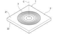
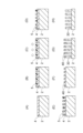
- FIG. 1 is a perspective view showing an optical element according to a first embodiment.
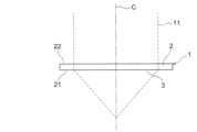
- 1 is a side view showing an optical element according to a first embodiment.
- 1A and 1B are diagrams illustrating a microstructure of an optical element according to a first embodiment.
- FIG. 1 is a diagram conceptually showing a microstructure of a first embodiment.
- 5A and 5B are schematic diagrams for explaining the optical characteristics of the microstructure of the first embodiment.
- 1A is a cross-sectional view showing the microstructure of embodiment 1
- FIG. 1B is a diagram showing its phase distribution.
- 1A is a cross-sectional view and FIG. 1B is a plan view showing a microstructure of the first embodiment.
- 1A to 1H show an example of a method for manufacturing the optical element according to the first embodiment.
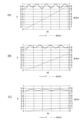
- 6A to 6C are graphs showing the relationship between the height of the structure and the transmittance and phase when the diameter of the structure of the microstructure of the first embodiment is changed.
- 10 is a graph showing the relationship between the height of the structure and the transmittance and phase when the diameter of the structure of the microstructure of the first embodiment is made larger than that of FIG. 9(A).
- 10 is a graph showing the relationship between the height of the structure and the transmittance and phase when the pitch of the fine structure of the first embodiment is made larger than that of FIG. 9(A).
- 1 is a graph showing the relationship between the height and phase of a structure for obtaining a transmittance equal to or greater than a specified value in the microstructure of the first embodiment.
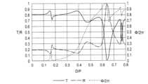
- the graph shows the relationship between the ratio of diameter to pitch and the transmittance, reflectance, and phase when the height and pitch of the structures are fixed and only the diameter is changed.
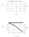
- Graph (A) shows the relationship between the structural parameters and the transmittance and phase when only the height and diameter of the structure are changed
- graph (B) shows the relationship between the structural parameters and the transmittance and phase when the height, diameter, and pitch of the structure are changed.
- 1A is a cross-sectional view showing a microstructure of embodiment 2
- FIG. 1B is a diagram showing its phase distribution.
- 1A is a perspective view
- FIG. 1B is a schematic view showing an example of an optical device to which the optical elements according to the first and second embodiments can be applied;
- Embodiment 1 ⁇ Overall configuration of optical element> First, a description will be given of an optical element 1 according to embodiment 1.
- Fig. 1 is a perspective view showing the optical element 1 according to embodiment 1.
- Fig. 2 is a side view showing the optical element 1.
- the optical element 1 of the first embodiment is a lens that focuses or collimates light. As shown in FIG. 2, the optical element 1 is formed by forming a microstructure 3, which is a concave-convex structure that changes the phase of light, on the surface 21 of a flat substrate 2.
- the microstructure 3 is also called a metasurface.
- the optical element 1 is also called a metalens.
- the wavelength of the light incident on the optical element 1 is, for example, less than 30 ⁇ m.
- One example is 400 nm to 2000 nm.
- Light in this wavelength band includes visible light and infrared light.
- the substrate 2 is made of a material that transmits light.
- the substrate 2 is made of Si or TiO2 .
- the refractive index of the substrate 2 may be 2 or more.
- the thickness of the substrate 2 is, for example, 0.3 mm or more and desirably 2.0 mm or less.
- the substrate 2 has a front surface 21 and a back surface 22, and a microstructure 3 is formed on the front surface 21.
- Fig. 3 is a plan view showing the microstructure 3 of the optical element 1.
- the microstructure 3 has a plurality of concentric ring zones A1, A2, A3...Am, where m is an integer of 2 or more.
- An imaginary line passing through the centers of the concentric ring zones A1 to Am and extending in the thickness direction of the substrate 2 is the optical axis C of the optical element 1.
- the ring zones A1, A2, A3...Am are arranged in this order from the side closest to the optical axis C.
- each of the rings A1 to Am (i.e. the radial dimension centered on the optical axis C) becomes narrower the further away from the optical axis C.
- Each of the rings A1 to Am is a band in which the phase change given to light is between 0 and 2 ⁇ .
- the rings A1 to Am are collectively referred to as ring A.
- Each annular zone A has multiple concentric regions B1, B2, B3...Bn centered on the optical axis C.
- n is an integer of 2 or more.
- Regions B1, B2, B3...Bn are arranged in this order from the side closest to the optical axis C.
- Regions B1 to Bn are collectively referred to as region B.
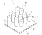
- FIG. 4 is a perspective view conceptually showing an example of the configuration of the microstructure 3.
- the microstructure 3 is a two-dimensional arrangement of multiple structures 30.
- the structures 30 are, for example, cylindrical, and are also called meta-atoms or pillars.
- the structure 30 has a height H in a direction perpendicular to the surface 21 of the substrate 2 (i.e., the direction of the optical axis C), and a width (more specifically, a diameter) D in a plane parallel to the surface 21 of the substrate 2. Furthermore, in the plane parallel to the surface 21 of the substrate 2, the center-to-center distance between adjacent structures 30 is the pitch P.
- Structures 30 differ in at least one of height H, diameter D, and pitch P depending on the regions B1, B2, B3, ... Bn ( Figure 3).
- at least one of height H, diameter D, and pitch P, including pitch P differs.
- Structures included in the same region e.g. region B1 have the same height H, same diameter D, and same pitch P.
- the shape of the structures 30 is not limited to a cylindrical shape, and may be, for example, a rectangular column shape.
- the diameter D of the structures 30 is also referred to as the width.
- the pitch P of the structures 30 is also referred to as the interval.
- phase that the structure 30 imparts to the light by linearly changing the phase that the structure 30 imparts to the light, it is possible to deflect (refract) the light that is incident on the optical element 1. Also, by changing the phase that the structure 30 imparts to the light like a Fresnel lens, it is possible to perform the function of concentrating the incident light 11, or the function of collimating light that is incident in a divergent state, as shown in FIG. 2. It is also possible to perform the function of branching or reflecting the incident light 11.
- Figures 5(A) and (B) are schematic diagrams for explaining the phase distribution when the optical element 1 is configured as a focusing lens or a collimating lens.
- the distance from the center of the optical element 1, i.e., the optical axis C, is r
- the phase at a position at a distance r from the center of the optical element 1 is ⁇ (r).
- the wavelength of the light incident on the optical element 1 is ⁇
- the focal length of the lens that is the optical element 1 is f.
- ⁇ (0) 2 ⁇
- the phase distribution is assumed to be one in which the phase is wrapped every 2 ⁇ .
- the optical element 1 is configured as a transmissive lens in which light is incident perpendicularly to the surface 21 of the substrate 2.
- the optical element 1 can also be configured as a reflective lens, a diffraction grating, or a reflective element by arranging the structures 30 according to the respective phase distributions.
- the bottom 32 (FIG. 4) of the structure 30 is positioned on the same plane, and the position of the top 31 (FIG. 4) of the structure 30 is varied, but this configuration is not limited thereto, and the top 31 of the structure 30 may be positioned on the same plane, and the position of the bottom 32 may be varied.
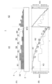
- Fig. 6(A) is a radial cross-sectional view that shows an outline of the structures 30 in regions B1 to B10 of the rings A1 and A2.
- Fig. 6(B) is a graph showing the phase ⁇ that the structures 30 in each region B of the rings A1 and A2 impart to light and the height H of the structures 30.
- the vertical axis on the left side of Figure 6(B) shows the phase ⁇ divided by 2 ⁇
- the vertical axis on the right side shows the height H divided by the wavelength ⁇
- the horizontal axis shows the distance r from the optical axis C.
- annular zone A is divided into multiple regions B, ten regions B in this case.
- annular zone A1 is made up of regions B1, B2, ... B10.
- the structure 30 in the first region B1 imparts a phase change of 2 ⁇ to light.
- the structure 30 in the tenth region B10 imparts a phase change of 0 to light. Note that although each annular zone A is divided into ten regions B1 to B10 in this case, the number of divisions is not limited to 10.
- At least one of the height H, diameter D, and pitch P of the structure 30 varies for each region B (i.e., for regions B1, B2, ... B10), thereby changing the phase imparted to the light.
- the height H, pitch P, and diameter D of the structure 30 are also referred to as structural parameters.
- the structure 30 in each region B imparts a phase change of at least 0 to 2 ⁇ to the light, allowing for flexibility in the design of the optical element 1. Note that while the structure 30 is configured here to impart a phase change of 0 to 2 ⁇ to the light, it may also be configured to impart a phase change of more than 2 ⁇ .
- the height H, diameter D, and pitch P of the structures 30 may be determined so as to suppress (or more preferably, prevent) light reflection at the interface between the structures 30 and air. This makes it possible to obtain an optical element 1 with high transmittance without forming an anti-reflection film, thereby enabling cost reduction.
- ⁇ Dimensions and layout of structure The arrangement of the structures 30 in the microstructure 3, as well as the height H, pitch P, and diameter D, are determined as follows: In a first step, for example, FEM (Finite Element Method) is used to vary the height H, diameter D, and pitch P within a certain range, and data on the phase and transmittance is accumulated.
- FEM Finite Element Method
- an ideal phase distribution is determined, as indicated by reference character K1 in FIG. 6B.
- This is, for example, the phase distribution of a Fresnel lens to be realized by the optical element 1.
- discrete values of the phase are determined for each of the regions B1, B2...B10. That is, the phase of region B1 is T1, the phase of region B2 is T2, ... and so on, determining the phases of regions B1, B2...B10.
- the height H, diameter D, and pitch P i.e., structural parameters
- the height H, diameter D, and pitch P are determined so that phase value T1 is obtained.
- the height H determined in this way is H/ ⁇ , and is shown by the symbol K3 in Figure 6 (B).
- the phase and transmittance data is accumulated using FEM, and the structural parameters are determined from the values obtained by discretizing the ideal phase distribution, but the phase of the structure 30 in each region may be calculated by analyzing the effective refractive index to determine the structural parameters.
- the phase of the structure 30 in each region may be calculated by analyzing the effective refractive index to determine the structural parameters.
- FEM Fluorescence-Emitter-Emitter-Emitter-Emitter-Wave Analysis
- Figures 7(A) and (B) are a plan view and a side view conceptually showing an enlarged view of areas B1 to B4 of zone A1 in microstructure 3.
- the structure 30 in region B1 has a height H1, a diameter D1, and a pitch P1.
- the structure 30 in region B2 has a height H2, a diameter D2, and a pitch P2.
- the structure 30 in region B3 has a height H3, a diameter D3, and a pitch P3.
- the structure 30 in region B4 has a height H4, a diameter D4, and a pitch P4.
- At least one of the height H, diameter D, and pitch P of the structures 30 may be different.
- the diameter D and pitch P of the structures 30 may be the same, and only the height H of the structures 30 may be different.
- the structures 30 are arranged in a triangular lattice pattern in each region B.
- the arrangement of the structures 30 is not limited to this example, and they may be arranged in a square lattice pattern, for example.
- arranging the structures 30 in a triangular lattice pattern allows for a higher packing rate of the structures 30 and allows for more flexible changes in phase than when the structures 30 are arranged in a square lattice pattern.
- the radial direction of the optical element 1 passing through the center of the optical element 1 is defined as the R direction.
- the circumferential direction of the optical element 1 centered on the optical axis C is defined as the L direction.
- the circumferential direction, L direction is shown as a straight line.
- a structure 30 is placed at the center of the optical element 1. This structure 30 is referred to as the first structure 30.
- the first structure 30 is assigned a height H, a diameter D, and a pitch P that, from the accumulated data described above, provide a phase that is closest to the discrete value of the phase at this position (i.e., the value on the curve K2 shown in FIG. 6(B)).
- the first structure 30 is included in region B1, and is therefore given height H1, diameter D1, and pitch P1.
- the second structure 30 is placed at a position that is pitch P1 away from the first structure 30.
- the structures 30 are arranged in a triangular lattice pattern, so the second structure 30 is placed at a position that is pitch P1 away from the first structure 30 in a direction that is inclined 30 degrees relative to the R direction.
- the second structure 30 is assigned a height H, diameter D, and pitch P that, from the stored data described above, provide a phase that is closest to the discrete value of the phase at this position.
- the second structure 30 is also included in region B1, and is therefore given a height H1, a diameter D1, and a pitch P1.
- the second structures 30 are arranged in a circumferential direction, i.e., in the L direction, at intervals of the given pitch P1.
- a third structure 30 is placed at a position that is pitch P1 away from the second structure 30.
- the third structure 30 is given a height H, diameter D, and pitch P that provide a phase that is closest to the discrete value of the phase at this position from the stored data described above.
- the third structure 30 is placed at a position that is pitch P1 away from the second structure 30 in a direction inclined 30 degrees with respect to the R direction.
- the third structure 30 is also included in region B1, and is therefore given a height H1, a diameter D1, and a pitch P1.
- the third structure 30 is arranged in a plurality of rows in the circumferential direction, i.e., in the L direction, at intervals of the given pitch P.
- the structures 30 are arranged in a triangular lattice pattern, but the structures 30 may also be arranged in a square lattice pattern.
- the second structure 30 is placed at a position spaced apart from the first structure 30 by pitch P1 in the R direction.
- FIGS. 8A to 8H are diagrams showing an example of a manufacturing process of the optical element 1.
- the microstructure 3 can be fabricated using, for example, electron beam lithography technology or deep ultraviolet lithography technology.
- a substrate 2 is prepared.
- the substrate 2 is made of Si or TiO 2 , and the thickness of the substrate 2 is preferably 0.3 mm to 2.0 mm.
- a metal mask layer 4 is formed on the surface of the substrate 2.
- resist 5 is applied onto the metal mask layer 4.
- the resist 5 is exposed using a mask that corresponds to the design shape of the microstructure 3, including the height H, diameter D, and pitch P of the structure 30.
- the resist 5 is developed. If the resist 5 is a negative type, the exposed parts remain, and if the resist 5 is a positive type, the exposed parts are removed.
- the metal mask layer 4 is patterned by dry etching or the like, using the resist 5 remaining after development as an etching mask. As a result, a metal layer 40 remains on the resist 5. Thereafter, as shown in FIG. 8(F), the resist 5 is removed.
- the substrate 2 is etched using the metal layer 40 on the resist 5 as an etching mask. This causes the surface of the substrate 2 to be patterned, and structures 30 are formed.
- the structures 30 have a height H, diameter D, and pitch P that correspond to their positions.
- the metal layer 40 is removed. This results in the formation of a microstructure 3 consisting of a plurality of structures 30 on the surface of the substrate 2.
- Methods for manufacturing structures 30 with different heights H include, for example, an exposure method using a grayscale mask, a method of drawing while modulating the intensity in electron beam exposure, a method using focused laser scanning, a method of repeating photolithography, etc.
- the optical element 1 is used, for example, as a lens of a camera or a sensor serving as an optical device (see FIGS. 16A and 16B described later).
- a camera generally includes a lens group formed by combining a plurality of lenses, but the lens group can be replaced with a single optical element 1 including a microstructure 3.
- the lens group may be constructed using a small number of aspherical lenses, but in the case of wide-angle lenses, an optical system with a high NA (Numerical Aperture) is required, which makes the lenses thicker and increases manufacturing costs.
- NA Numerical Aperture
- the thickness will be 4.5 mm or more even if the lens is made of Si (silicon), which has a high refractive index. If glass, which has a low refractive index, is used, the thickness will be more than twice as thick, and the shape may be difficult to manufacture.
- an optical element 1 with a microstructure 3 it is possible to manufacture lenses with a thickness of 2.0 mm or less (preferably 1.0 mm or less), making it possible to reduce the size and weight of optical devices incorporating the lenses.
- the focused spot needs to be made smaller in order to increase the resolution.
- the smaller the focused spot the longer it takes to expose the entire lens surface, and more expensive exposure devices are required, which increases manufacturing costs.
- the height H, diameter D, and pitch P of the structures 30 are changed, so even if the height H, diameter D, and pitch P are controlled relatively roughly, the resolution of the phase of the light changed by the microstructure 3 can be increased. Therefore, even if an exposure device with a relatively low resolution is used, a high-performance lens can be manufactured.
- Fig. 9(A) is a graph showing the change in the transmittance T and the phase difference ⁇ /2 ⁇ when the diameter D and pitch P of the structure 30 are fixed and the height H is changed.
- the vertical axis on the left side of Fig. 9(A) shows the transmittance T, and the vertical axis on the right side shows the value obtained by dividing the phase difference ⁇ by 2 ⁇ .
- the horizontal axis shows the height H of the structure 30.
- FIG. 9(B) is a graph showing the relationship between the height H of the structure 30 and the transmittance T and phase difference ⁇ /2 ⁇ when the diameter D is smaller than that of FIG. 9(A) but the pitch P is the same as that of FIG. 9(A).
- FIG. 9(C) is a graph showing the relationship between the height H of the structure 30 and the transmittance T and phase difference ⁇ /2 ⁇ when the diameter D is smaller than that of FIG. 9(B) but the pitch P is the same as that of FIG. 9(A).
- the vertical and horizontal axes are the same as those of FIG. 9(A).
- Figure 10 is a graph showing the relationship between height H, transmittance T, and phase difference ⁇ /2 ⁇ when the pitch P is the same as in Figure 9(A) but the diameter D is larger than in Figure 9(A).
- the vertical and horizontal axes are the same as in Figure 9(A).
- the change in transmittance T with respect to the change in height H is no longer periodic, and the transmittance T changes abruptly, resulting in portions where the transmittance is 0.1 or less.
- Figure 11 is a graph showing the relationship between height H, transmittance T, and phase difference ⁇ /2 ⁇ when the diameter D is the same as in Figure 9(A) but the pitch P is larger than in Figure 9(A).
- the vertical and horizontal axes are the same as in Figure 9(A).
- the optical element 1 To make the design of the optical element 1 easier, it is desirable to avoid combinations of diameter D and pitch P in which the transmittance T changes drastically with changes in height H (see Figure 10).
- the height H is changed among multiple combinations of diameter D and pitch P, and a combination of height H, diameter D, and pitch P that results in a high transmittance T is adopted. This makes it possible to change the phase while suppressing reflected light.
- FIG. 12 is a graph showing the relationship between the height H of the structure 30 and the phase difference ⁇ /2 ⁇ , which provides a transmittance of 96% or more when the target light wavelength is 685 nm and the optical element 1 is designed with a TiO 2 substrate.
- the graph also shows the relationship between the phase difference ⁇ /(2 ⁇ ) and the height H of the structure 30, which provides a transmittance of 85% or more when the target light wavelength is 905 nm and the optical element 1 is designed with a Si substrate.
- the vertical axis of FIG. 12 shows the value obtained by dividing the phase difference ⁇ by 2 ⁇ , and the horizontal axis shows the value obtained by dividing the height H by the wavelength ⁇ .
- ⁇ is the wavelength of light.
- the diameter D and pitch P of the structures 30 are desirable to suppress the decrease and the fluctuation of the transmittance T.
- the diameter D of the structures 30 within a range of 150 nm to 250 nm and the pitch P within a range of 300 nm to 450 nm.
- the diameter D of the structure 30 is desirably set within the range of ⁇ 150 nm to ⁇ 250 nm
- the pitch P is desirably set within the range of ⁇ 300 nm to ⁇ 450 nm.
- the lower limit of the above-mentioned range of diameter D, ⁇ 150 nm can be expressed as 150 ⁇ (n 0 / ⁇ 0 ) ⁇ ( ⁇ /n)
- the upper limit of the range, ⁇ 250 nm can be expressed as 250 ⁇ (n 0 / ⁇ 0 ) ⁇ ( ⁇ /n).
- the range of diameter D of structure 30 can be expressed as 0.56 ⁇ /n to 0.95 ⁇ /n.
- the range of pitch P of structure 30 can be expressed as 1.1 ⁇ /n to 1.7 ⁇ /n.
- the diameter D and pitch P of the structures 30 differ for each region B, but in all regions B1 to Bn ( Figure 3), it is desirable that the diameter D of the structures 30 be within the range of 0.56 x ⁇ /n to 0.95 x ⁇ /n, and the pitch P of the structures 30 be within the range of 1.1 x ⁇ /n to 1.7 x ⁇ /n.
- Equation (2) shows the relationship between the height H/ ⁇ of the structure 30 and the phase difference ⁇ /2 ⁇ , but there are manufacturing limitations. That is, for example, if the ratio of the diameter D to the pitch P of the structure 30 exceeds 0.8 (i.e., D/P>0.8), the ratio of the area of the structure 30 to the surface area of the substrate 2 increases, the aspect ratio increases, and etching becomes difficult.
- the diameter D and pitch P of the structure 30 may be set to a certain fixed width (for example, in 10 nm increments). If the width of the diameter D and pitch P is set small, a high-resolution exposure device must be used when manufacturing the microstructure 3. When designing the structure 30, the number of combinations of height H, diameter D, and pitch P that must be considered increases, making it difficult to obtain the relationship with the phase.
- the diameter D and pitch P may be set in increments of an integer multiple of 5 nm, such as 5 nm increments or 15 nm increments. Furthermore, they are not limited to being set in increments of an integer multiple of 5 nm, and may be set in increments of several nm to several tens of nm. Furthermore, not only the diameter D and pitch P but also the height H may be set in increments of a specified value.
- phase ⁇ and height H of the structure 30 has been explained above. Below, the relationship between the phase ⁇ and diameter D and pitch P of the structure 30 will be explained.
- the wavelength of the target light is ⁇
- the refractive index of air is n a
- the effective refractive index of the structure 30 is n eff .
- the phase at the center position of the optical element 1 i.e., the optical axis C
- the phase change caused by the structure 30 is expressed by the following equation (3).
- the effective refractive index n eff is expressed by the following equation (4), which is a simple approximation, using the refractive index n a of air, the refractive index n s of the substrate 2 before processing of the microstructure 3 (i.e., the substrate 2 shown in FIG. 8(A)), and the diameter D and pitch P of the structures 30.
- the effective refractive index n eff can be well approximated by equation (4).
- the actual effective refractive index will be smaller than the effective refractive index calculated by equation (4).
- n(h) eff of a diffraction grating is expressed by the following formula (5), where h is the height of the diffraction grating.
- n(0) eff is the effective refractive index of a diffraction grating with a height of 0.
- nL is the effective refractive index when the height h of the diffraction grating is regarded as infinity, and is calculated by the above formula (4).
- (dn(h)2eff ) /(d(hk)) represents the second derivative of n(h)2eff .
- the effective refractive index is calculated by numerically solving this differential equation.
- the height h of the diffraction grating in equation (5) can be replaced with the height H of the structure 30 in this embodiment.
- the exact effective refractive index can be obtained using numerical simulations such as RCWA, FEM, and FDTD (Finite-Difference-Time-Domain) methods.
- the above-mentioned Figures 9(A) to 12 show the results of obtaining the phase ⁇ and transmittance T when the structural parameters of the structure 30 are changed by numerical simulation using FEM.
- Fig. 13 shows the analysis results of the transmittance T, reflectance R, and phase difference ⁇ / 2 ⁇ when the height H and pitch P of the structures 30 are fixed and only the diameter D is changed, where the wavelength of the target light is 685 nm and the optical element 1 is made of TiO2.
- the vertical axis on the left side of Figure 13 indicates the transmittance T and reflectance R, and the vertical axis on the right side indicates the phase difference ⁇ /2 ⁇ .
- the horizontal axis indicates the value (D/P) obtained by dividing the diameter D by the pitch P.
- the transmittance of the optical element 1 Due to reflection at the interface caused by the difference in refractive index between the optical element 1 (lens in this case) and air, the transmittance of the optical element 1 is generally low, at about 80%.
- the reflectance RF due to Fresnel reflection at the interface can be expressed by the following equation (6).
- the reflectance R of the structure 30 is smaller than the reflectance RF due to Fresnel reflection.
- the transmittance becomes approximately 0%.
- Figure 14 (A) is a graph showing the relationship between the combination of structural parameters (height H, diameter D, pitch P) that results in a transmittance T of 99.5% or more when the pitch P is fixed, the diameter D is changed in increments of 10 nm, and the height H is changed in increments of 20 nm, and the transmittance T and phase difference ⁇ /2 ⁇ .
- the vertical axis on the left side shows the transmittance T
- the vertical axis on the right side shows the phase difference ⁇ /2 ⁇
- the horizontal axis shows the number (set number) i that indicates the combination.
- Figure 14(B) is a graph showing the relationship between the combination of structural parameters (height H, diameter D, pitch P) that results in a transmittance T of 99.5% or more when the diameter D and pitch P are each changed in increments of 10 nm and the height H is changed in increments of 20 nm, and the transmittance T and phase difference ⁇ /2 ⁇ .
- the vertical axis on the left side shows the transmittance T
- the vertical axis on the right side shows the phase difference ⁇ /2 ⁇
- the horizontal axis shows the number (set number) i that indicates the combination.
- FIG. 14(A) only the height H and diameter D are changed, so the number of combinations of structural parameters (i) is small, resulting in a sparse phase distribution.
- FIG. 14(A) there are no combinations of structural parameters that result in a phase difference ⁇ /2 ⁇ in the range of 0.6 to 0.7. In other words, defects occur in the range of 0.1 or more for the phase difference ⁇ /2 ⁇ . As a result, the precision of the phase distribution that the optical element 1 imparts to light is reduced.
- the optical element 1 of the first embodiment has a microstructure 3 that changes the phase of light on the surface of the substrate 2, and the microstructure 3 has a plurality of structures 30.
- the height H, diameter (i.e., width) D, and pitch (i.e., interval) P of the structures 30 vary depending on the region B in the microstructure 3. Therefore, the phase distribution can be controlled with high precision without increasing the resolution of the exposure apparatus, and the manufacturing cost of the optical element 1 can be reduced.
- the wavelength of light is ⁇ and the refractive index of the substrate 2 is n, then by setting the pitch P of the structures 30 to 1.1 ⁇ /n to 1.7 ⁇ /n, it is possible to increase the transmittance of the optical element 1 and suppress variations in the transmittance.
- the transmittance of the optical element 1 can be increased and the variation in the transmittance can be suppressed.
- the pitch P of the structures 30 is set in specified increments (e.g., 10 nm increments) by region B within the microstructure 3, and the diameter width D of the structures 30 is set in specified increments (e.g., 10 nm increments), so the phase distribution can be controlled with high precision without increasing the resolution of the exposure device.
- the structure 30 has a height H, a diameter D, and a pitch P that suppress light reflection at the interface between the structure 30 and air, an optical element 1 with high transmittance can be obtained without providing an anti-reflection film or the like, further improving manufacturing costs.
- the height H of the structure 30 is determined as expressed by the above formula (2), an optical element 1 with high transmittance can be obtained even if the wavelength of light or the material of the substrate 2 is changed.
- the phase distribution in the two or more regions B can be controlled simply by changing the etching depth.
- the target light is one with a wavelength of less than 30 ⁇ m
- an optical element 1 that can be used for both visible light and infrared light can be obtained.
- the microstructure 3 is divided into a number of concentric ring zones A1 to Am with a phase difference of 2 ⁇ , and each ring zone A is divided into a number of concentric regions B1 to Bn, and the multiple structures 30 contained in each region B have the same height H, diameter D, and pitch P. Therefore, it is possible to realize an optical element 1 that has the same function as, for example, a Fresnel lens.
- the reflectance of light at the optical element 1 is smaller than the reflectance calculated by Fresnel diffraction from the refractive index n of the substrate 2 and the refractive index of air, it is possible to reduce the reflection and absorption of light at the interface between the optical element 1 and the air.
- the thickness of the optical element 1 2 mm or less it becomes possible to mount it on a thin optical device 8, which contributes to making the optical device 8 smaller and lighter.
- the structures 30 are arranged so as to approximate the ideal phase distribution.
- the structures 30 are arranged so as to approximate the ideal phase distribution while decreasing the height of the structures 30 as the phase given to the light decreases.
- the microstructure 3A has a plurality of concentric ring zones A1, A2, A3...Am.
- Each ring zone A has a plurality of concentric regions B1, B2, B3...Bn.
- the ring zone A is divided into six regions B1 to B6, but the number of divisions is not limited to six and can be any number.
- a plurality of structures 30 are arranged in each region B.
- Figure 15(A) is a cross-sectional view along the radial direction, which shows a schematic diagram of the structure 30 in each region B of the rings A1 and A2.
- Figure 15(B) is a graph showing the phase ⁇ that the structure 30 in each region B of the rings A1 and A2 imparts to light, and the height H of the structure 30.
- the vertical and horizontal axes are the same as those in Figure 6(B).
- the structures 30 in each of the regions B1 to B6 are arranged so that the height H of the structures 30 in each region B is equal to or less than the height H of the structures 30 in the region B that is closer to the center (optical axis C) of the optical element 1.
- the height H of the structure 30 in region B2 is lower than the height H of the structure 30 in region B1. Also, the height H of the structure 30 in region B3 is lower than the height H of the structure 30 in region B2. The same is true for the structures 30 in regions B4 to B6.
- the manufacturing process of the optical element 1A of the second embodiment is generally similar to the manufacturing process of the optical element 1 of the first embodiment (FIGS. 8(A)-(H)).
- the optical element 1A of the second embodiment sudden changes in the height of the structures 30 are suppressed, improving the processability in the etching process of the substrate 2 (FIG. 8(G)). This simplifies the manufacturing process and reduces manufacturing costs.
- the height H, diameter D, and pitch P of each structure 30 are determined so that the phase in each structure 30 is closest to the discretized value (K2 in FIG. 15B) of the ideal phase distribution (K1 in FIG. 15B).
- the height H of the structures 30 in each region B is determined to be equal to or less than the height H of the structures 30 in a region B that is closer to the center of the optical element 1A than that region B.
- the optical element 1A of the second embodiment is configured similarly to the optical element 1 of the first embodiment.
- the height of the structures 30 in each region B of the microstructure 3A is equal to or less than the height H of the structures 30 in the region B that is closer to the center of the optical element 1A than the region B, and therefore abrupt changes in the height of the structures 30 are suppressed. This makes it possible to improve the workability of the etching process of the substrate 2 and reduce manufacturing costs.
- the following provides additional information on the method for analyzing the shape of the microstructures 3, 3A (i.e., metasurfaces) of the optical elements 1, 1A of the first and second embodiments.
- a method that utilizes scattering by a Mie resonator is known as a method for analyzing three-dimensional structures such as spheres or ellipsoids, but this method is difficult to apply to microstructures having structures of arbitrary shapes (i.e., meta-atoms).
- Electromagnetic field simulation is desirable as a method for analyzing the microstructures 3, 3A of complex shapes. Specifically, the above-mentioned FDTD, RCWA, and FEM, as well as BPM (Beam Promotion Method), etc. are desirable.
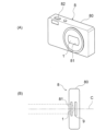
- FIG. 16(A) is a perspective view showing the appearance of an optical device 8 equipped with the optical element 1
- FIG. 16(B) is a schematic diagram showing the internal configuration of the optical device 8.
- the optical element 1 is used as a lens of the optical device 8.
- the optical device 8 has an optical element 1, a light receiving element 9 arranged on the optical axis C of the optical element 1, and a housing 80 that covers them.
- An opening 81 is formed on the front of the housing 80 so as to face the optical element 1.
- a switch 82 and the like that are used when capturing an image are provided.
- the optical element 1 forms an image of the subject on the light receiving element 9, and the light receiving element 9 converts the received optical signal into an electrical signal.
- a camera generally has a lens group made up of a combination of multiple lenses, but the lens group can be replaced with the optical element 1.
- the optical element 1 is thin, and can be made, for example, 2 mm or less, making it possible to realize a thin and compact optical device 8.
- the optical element 1 is not limited to being a camera, and can also be realized as a sensor or other optical device.
Landscapes
- Physics & Mathematics (AREA)
- General Physics & Mathematics (AREA)
- Optics & Photonics (AREA)
- Diffracting Gratings Or Hologram Optical Elements (AREA)
Priority Applications (3)
| Application Number | Priority Date | Filing Date | Title |
|---|---|---|---|
| PCT/JP2022/045754 WO2024127479A1 (ja) | 2022-12-13 | 2022-12-13 | 光学素子および光学装置 |
| JP2024563798A JPWO2024127479A1 (https=) | 2022-12-13 | 2022-12-13 | |
| CN202280102095.0A CN120283181A (zh) | 2022-12-13 | 2022-12-13 | 光学元件和光学装置 |
Applications Claiming Priority (1)
| Application Number | Priority Date | Filing Date | Title |
|---|---|---|---|
| PCT/JP2022/045754 WO2024127479A1 (ja) | 2022-12-13 | 2022-12-13 | 光学素子および光学装置 |
Publications (1)
| Publication Number | Publication Date |
|---|---|
| WO2024127479A1 true WO2024127479A1 (ja) | 2024-06-20 |
Family
ID=91484513
Family Applications (1)
| Application Number | Title | Priority Date | Filing Date |
|---|---|---|---|
| PCT/JP2022/045754 Ceased WO2024127479A1 (ja) | 2022-12-13 | 2022-12-13 | 光学素子および光学装置 |
Country Status (3)
| Country | Link |
|---|---|
| JP (1) | JPWO2024127479A1 (https=) |
| CN (1) | CN120283181A (https=) |
| WO (1) | WO2024127479A1 (https=) |
Citations (5)
| Publication number | Priority date | Publication date | Assignee | Title |
|---|---|---|---|---|
| CN106125176A (zh) * | 2016-07-11 | 2016-11-16 | 中国科学院上海技术物理研究所 | 一种太赫兹一维立体相位光栅 |
| US20180292644A1 (en) * | 2017-04-10 | 2018-10-11 | California Institute Of Technology | Tunable Elastic Dielectric Metasurface Lenses |
| JP2019516128A (ja) * | 2016-04-05 | 2019-06-13 | プレジデント・アンド・フェロウズ・オブ・ハーバード・カレッジ | サブ波長解像度イメージング用のメタレンズ |
| JP2021099399A (ja) * | 2019-12-20 | 2021-07-01 | 浜松ホトニクス株式会社 | テラヘルツ波用レンズ及びテラヘルツ波用レンズの製造方法 |
| JP2021193467A (ja) * | 2016-08-22 | 2021-12-23 | マジック リープ, インコーポレイテッドMagic Leap, Inc. | ウェアラブルディスプレイデバイスのためのディザリング方法および装置 |
-
2022
- 2022-12-13 JP JP2024563798A patent/JPWO2024127479A1/ja active Pending
- 2022-12-13 CN CN202280102095.0A patent/CN120283181A/zh active Pending
- 2022-12-13 WO PCT/JP2022/045754 patent/WO2024127479A1/ja not_active Ceased
Patent Citations (5)
| Publication number | Priority date | Publication date | Assignee | Title |
|---|---|---|---|---|
| JP2019516128A (ja) * | 2016-04-05 | 2019-06-13 | プレジデント・アンド・フェロウズ・オブ・ハーバード・カレッジ | サブ波長解像度イメージング用のメタレンズ |
| CN106125176A (zh) * | 2016-07-11 | 2016-11-16 | 中国科学院上海技术物理研究所 | 一种太赫兹一维立体相位光栅 |
| JP2021193467A (ja) * | 2016-08-22 | 2021-12-23 | マジック リープ, インコーポレイテッドMagic Leap, Inc. | ウェアラブルディスプレイデバイスのためのディザリング方法および装置 |
| US20180292644A1 (en) * | 2017-04-10 | 2018-10-11 | California Institute Of Technology | Tunable Elastic Dielectric Metasurface Lenses |
| JP2021099399A (ja) * | 2019-12-20 | 2021-07-01 | 浜松ホトニクス株式会社 | テラヘルツ波用レンズ及びテラヘルツ波用レンズの製造方法 |
Also Published As
| Publication number | Publication date |
|---|---|
| JPWO2024127479A1 (https=) | 2024-06-20 |
| CN120283181A (zh) | 2025-07-08 |
Similar Documents
| Publication | Publication Date | Title |
|---|---|---|
| US10551531B2 (en) | Hybrid diffraction grating, mold insert and manufacturing methods thereof | |
| US8878122B2 (en) | Two dimensional solid-state image pickup device with a light condensing element including protrusions separated by recesses | |
| JP4630393B2 (ja) | 回折レンズ、およびこれを用いた撮像装置 | |
| CN108351437B (zh) | 扩散板、扩散板的设计方法、扩散板的制造方法、显示装置、投影装置和照明装置 | |
| CN103459995B (zh) | 光学波长分光装置及其制造方法 | |
| CN111527421B (zh) | 凹凸构造体、光学部件及电子设备 | |
| CN113009608B (zh) | 太赫兹波用透镜和太赫兹波用透镜的制造方法 | |
| JP2019139163A (ja) | 拡散板、拡散板の設計方法、表示装置、投影装置及び照明装置 | |
| CN113009603B (zh) | 太赫兹波用光学元件和太赫兹波用光学元件的制造方法 | |
| US20250004171A1 (en) | Optical lens, optical system, and imaging device | |
| US20040247010A1 (en) | Antireflection diffraction grating | |
| JPWO2011105067A1 (ja) | 回折レンズ、およびこれを用いた撮像装置 | |
| JP2004510194A (ja) | 屈折率分布型マイクロレンズ並びに設計及び形成方法 | |
| JP2005084485A (ja) | 回折光学素子 | |
| US20260016620A1 (en) | Optical lens and method for fabricating the same | |
| JP2586703B2 (ja) | 光学レンズ | |
| US20110235178A1 (en) | Diffractive optical element and optical device | |
| WO2024127479A1 (ja) | 光学素子および光学装置 | |
| US20250004172A1 (en) | Optical lens | |
| US20250028091A1 (en) | Optical element, optical system, lens apparatus, and image pickup apparatus | |
| JP7483948B2 (ja) | 拡散板、発光デバイス及びセンサモジュール | |
| JP2019066756A (ja) | 回折光学素子を備えた光学系および光学機器 | |
| US20230333288A1 (en) | Protective structures for manufacture of metasurfaces | |
| JP2001296649A (ja) | 濃度分布マスクとその製造方法及び表面形状の形成方法 | |
| JPH07113906A (ja) | 回折光学素子 |
Legal Events
| Date | Code | Title | Description |
|---|---|---|---|
| 121 | Ep: the epo has been informed by wipo that ep was designated in this application |
Ref document number: 22968391 Country of ref document: EP Kind code of ref document: A1 |
|
| WWE | Wipo information: entry into national phase |
Ref document number: 2024563798 Country of ref document: JP |
|
| WWE | Wipo information: entry into national phase |
Ref document number: 202280102095.0 Country of ref document: CN |
|
| WWP | Wipo information: published in national office |
Ref document number: 202280102095.0 Country of ref document: CN |
|
| NENP | Non-entry into the national phase |
Ref country code: DE |
|
| 122 | Ep: pct application non-entry in european phase |
Ref document number: 22968391 Country of ref document: EP Kind code of ref document: A1 |