WO2024122172A1 - 基板処理方法、半導体装置の製造方法、基板処理装置、及びプログラム - Google Patents
基板処理方法、半導体装置の製造方法、基板処理装置、及びプログラム Download PDFInfo
- Publication number
- WO2024122172A1 WO2024122172A1 PCT/JP2023/036230 JP2023036230W WO2024122172A1 WO 2024122172 A1 WO2024122172 A1 WO 2024122172A1 JP 2023036230 W JP2023036230 W JP 2023036230W WO 2024122172 A1 WO2024122172 A1 WO 2024122172A1
- Authority
- WO
- WIPO (PCT)
- Prior art keywords
- film
- groove
- stopper
- substrate
- substrate processing
- Prior art date
- Legal status (The legal status is an assumption and is not a legal conclusion. Google has not performed a legal analysis and makes no representation as to the accuracy of the status listed.)
- Ceased
Links
Images






Classifications
-
- H—ELECTRICITY
- H10—SEMICONDUCTOR DEVICES; ELECTRIC SOLID-STATE DEVICES NOT OTHERWISE PROVIDED FOR
- H10P—GENERIC PROCESSES OR APPARATUS FOR THE MANUFACTURE OR TREATMENT OF DEVICES COVERED BY CLASS H10
- H10P50/00—Etching of wafers, substrates or parts of devices
- H10P50/20—Dry etching; Plasma etching; Reactive-ion etching
- H10P50/28—Dry etching; Plasma etching; Reactive-ion etching of insulating materials
- H10P50/282—Dry etching; Plasma etching; Reactive-ion etching of insulating materials of inorganic materials
- H10P50/283—Dry etching; Plasma etching; Reactive-ion etching of insulating materials of inorganic materials by chemical means
-
- H—ELECTRICITY
- H10—SEMICONDUCTOR DEVICES; ELECTRIC SOLID-STATE DEVICES NOT OTHERWISE PROVIDED FOR
- H10P—GENERIC PROCESSES OR APPARATUS FOR THE MANUFACTURE OR TREATMENT OF DEVICES COVERED BY CLASS H10
- H10P14/00—Formation of materials, e.g. in the shape of layers or pillars
- H10P14/60—Formation of materials, e.g. in the shape of layers or pillars of insulating materials
- H10P14/65—Formation of materials, e.g. in the shape of layers or pillars of insulating materials characterised by treatments performed before or after the formation of the materials
- H10P14/6516—Formation of materials, e.g. in the shape of layers or pillars of insulating materials characterised by treatments performed before or after the formation of the materials of treatments performed after formation of the materials
- H10P14/6548—Formation of materials, e.g. in the shape of layers or pillars of insulating materials characterised by treatments performed before or after the formation of the materials of treatments performed after formation of the materials by forming intermediate materials, e.g. capping layers or diffusion barriers
-
- H—ELECTRICITY
- H10—SEMICONDUCTOR DEVICES; ELECTRIC SOLID-STATE DEVICES NOT OTHERWISE PROVIDED FOR
- H10P—GENERIC PROCESSES OR APPARATUS FOR THE MANUFACTURE OR TREATMENT OF DEVICES COVERED BY CLASS H10
- H10P14/00—Formation of materials, e.g. in the shape of layers or pillars
- H10P14/60—Formation of materials, e.g. in the shape of layers or pillars of insulating materials
-
- H—ELECTRICITY
- H10—SEMICONDUCTOR DEVICES; ELECTRIC SOLID-STATE DEVICES NOT OTHERWISE PROVIDED FOR
- H10P—GENERIC PROCESSES OR APPARATUS FOR THE MANUFACTURE OR TREATMENT OF DEVICES COVERED BY CLASS H10
- H10P14/00—Formation of materials, e.g. in the shape of layers or pillars
- H10P14/60—Formation of materials, e.g. in the shape of layers or pillars of insulating materials
- H10P14/63—Formation of materials, e.g. in the shape of layers or pillars of insulating materials characterised by the formation processes
- H10P14/6326—Deposition processes
- H10P14/6328—Deposition from the gas or vapour phase
- H10P14/6334—Deposition from the gas or vapour phase using decomposition or reaction of gaseous or vapour phase compounds, i.e. chemical vapour deposition
- H10P14/6339—Deposition from the gas or vapour phase using decomposition or reaction of gaseous or vapour phase compounds, i.e. chemical vapour deposition deposition by cyclic CVD, e.g. ALD, ALE or pulsed CVD
-
- H—ELECTRICITY
- H10—SEMICONDUCTOR DEVICES; ELECTRIC SOLID-STATE DEVICES NOT OTHERWISE PROVIDED FOR
- H10P—GENERIC PROCESSES OR APPARATUS FOR THE MANUFACTURE OR TREATMENT OF DEVICES COVERED BY CLASS H10
- H10P14/00—Formation of materials, e.g. in the shape of layers or pillars
- H10P14/60—Formation of materials, e.g. in the shape of layers or pillars of insulating materials
- H10P14/65—Formation of materials, e.g. in the shape of layers or pillars of insulating materials characterised by treatments performed before or after the formation of the materials
- H10P14/6516—Formation of materials, e.g. in the shape of layers or pillars of insulating materials characterised by treatments performed before or after the formation of the materials of treatments performed after formation of the materials
- H10P14/6529—Formation of materials, e.g. in the shape of layers or pillars of insulating materials characterised by treatments performed before or after the formation of the materials of treatments performed after formation of the materials by exposure to a gas or vapour
-
- H—ELECTRICITY
- H10—SEMICONDUCTOR DEVICES; ELECTRIC SOLID-STATE DEVICES NOT OTHERWISE PROVIDED FOR
- H10P—GENERIC PROCESSES OR APPARATUS FOR THE MANUFACTURE OR TREATMENT OF DEVICES COVERED BY CLASS H10
- H10P50/00—Etching of wafers, substrates or parts of devices
-
- H—ELECTRICITY
- H10—SEMICONDUCTOR DEVICES; ELECTRIC SOLID-STATE DEVICES NOT OTHERWISE PROVIDED FOR
- H10P—GENERIC PROCESSES OR APPARATUS FOR THE MANUFACTURE OR TREATMENT OF DEVICES COVERED BY CLASS H10
- H10P50/00—Etching of wafers, substrates or parts of devices
- H10P50/20—Dry etching; Plasma etching; Reactive-ion etching
- H10P50/26—Dry etching; Plasma etching; Reactive-ion etching of conductive or resistive materials
- H10P50/264—Dry etching; Plasma etching; Reactive-ion etching of conductive or resistive materials by chemical means
- H10P50/266—Dry etching; Plasma etching; Reactive-ion etching of conductive or resistive materials by chemical means by vapour etching only
- H10P50/267—Dry etching; Plasma etching; Reactive-ion etching of conductive or resistive materials by chemical means by vapour etching only using plasmas
- H10P50/268—Dry etching; Plasma etching; Reactive-ion etching of conductive or resistive materials by chemical means by vapour etching only using plasmas of silicon-containing layers
-
- H—ELECTRICITY
- H10—SEMICONDUCTOR DEVICES; ELECTRIC SOLID-STATE DEVICES NOT OTHERWISE PROVIDED FOR
- H10P—GENERIC PROCESSES OR APPARATUS FOR THE MANUFACTURE OR TREATMENT OF DEVICES COVERED BY CLASS H10
- H10P50/00—Etching of wafers, substrates or parts of devices
- H10P50/71—Etching of wafers, substrates or parts of devices using masks for conductive or resistive materials
-
- H—ELECTRICITY
- H10—SEMICONDUCTOR DEVICES; ELECTRIC SOLID-STATE DEVICES NOT OTHERWISE PROVIDED FOR
- H10P—GENERIC PROCESSES OR APPARATUS FOR THE MANUFACTURE OR TREATMENT OF DEVICES COVERED BY CLASS H10
- H10P50/00—Etching of wafers, substrates or parts of devices
- H10P50/73—Etching of wafers, substrates or parts of devices using masks for insulating materials
-
- H—ELECTRICITY
- H10—SEMICONDUCTOR DEVICES; ELECTRIC SOLID-STATE DEVICES NOT OTHERWISE PROVIDED FOR
- H10P—GENERIC PROCESSES OR APPARATUS FOR THE MANUFACTURE OR TREATMENT OF DEVICES COVERED BY CLASS H10
- H10P72/00—Handling or holding of wafers, substrates or devices during manufacture or treatment thereof
- H10P72/04—Apparatus for manufacture or treatment
- H10P72/0402—Apparatus for fluid treatment
- H10P72/0418—Apparatus for fluid treatment for etching
- H10P72/0421—Apparatus for fluid treatment for etching for drying etching
-
- H—ELECTRICITY
- H10—SEMICONDUCTOR DEVICES; ELECTRIC SOLID-STATE DEVICES NOT OTHERWISE PROVIDED FOR
- H10P—GENERIC PROCESSES OR APPARATUS FOR THE MANUFACTURE OR TREATMENT OF DEVICES COVERED BY CLASS H10
- H10P72/00—Handling or holding of wafers, substrates or devices during manufacture or treatment thereof
- H10P72/04—Apparatus for manufacture or treatment
- H10P72/0431—Apparatus for thermal treatment
Definitions
- This disclosure relates to a substrate processing method, a semiconductor device manufacturing method, a substrate processing apparatus, and a program.
- the present disclosure aims to provide a technique that enables precise removal of desired portions of a film when etching the film on a substrate.
- FIG. 2 is a schematic configuration diagram of a vertical processing furnace of a substrate processing apparatus suitably used in one embodiment of the present disclosure, showing a processing furnace 202 portion in vertical cross section.
- FIG. 2 is a schematic configuration diagram of a vertical processing furnace of a substrate processing apparatus suitably used in one embodiment of the present disclosure, showing a processing furnace 202 portion in a cross-sectional view taken along line AA of FIG. 1 is a schematic configuration diagram of a controller 121 of a substrate processing apparatus suitably used in one embodiment of the present disclosure, and is a block diagram showing a control system of the controller 121.
- FIG. FIG. 1 is a diagram showing a processing sequence according to an embodiment of the present disclosure.
- FIG. 1 is a cross-sectional view of a wafer 200 on which a first film portion 310, a second film portion 320, a third film portion 330, and a fourth film portion 340 are formed in one embodiment of the present disclosure.
- FIG. 2 is a perspective view of a wafer 200 according to one embodiment of the present disclosure. 2 is a cross-sectional view of a wafer 200 being processed in a substrate processing step according to one aspect of the present disclosure.
- 6B is a cross-sectional view showing a state in which a hard mask 900 is provided on the second film portion 320 of the wafer 200 to form a groove portion 350, following the state shown in FIG. 6A.
- FIG. 1 is a cross-sectional view of a wafer 200 on which a first film portion 310, a second film portion 320, a third film portion 330, and a fourth film portion 340 are formed in one embodiment of the present disclosure.
- FIG. 2 is a perspective view of a wafer 200 according
- 6C is a cross-sectional view showing a state in which the hard mask 900 has been removed from the state shown in FIG. 6B.
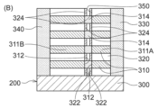
- This is a figure explaining the process of forming a stopper portion 314 on the first film portion 310 of the wafer 200 in one embodiment of the present disclosure, and is a cross-sectional view of the state in which a modified layer 324 has been formed on the second end surface 322 of the second film portion 320.
- 7B is a cross-sectional view of a state in which a stopper portion 314 is formed between first end surfaces 312 of first membrane portions 310 in the state of FIG. 7A.
- FIG. 7C is a cross-sectional view of a state in which the modified layer 324 on the second end surface 322 of the second membrane portion 320 has been removed from the state of FIG. 7B.
- 7D is a cross-sectional view of a state in which the groove portion 350 is backfilled with a second film portion 320 following the state of FIG. 7C.
- FIG. 13 is a cross-sectional view of a state in which a hard mask 910 is formed on the second film portion 320 in one embodiment of the present disclosure.
- 8B is a cross-sectional view showing a state in which a first portion 311A of a first film portion 310 and a third film portion 330 are removed from the state shown in FIG. 8A, and then a hard mask 910 is removed.
- FIG. 8C is a cross-sectional view showing a state in which a hard mask 920 is provided on the second film portion 320 and the stopper portion 314 is removed from the state shown in FIG. 8B.
- FIG. 8D is a cross-sectional view of a state in which the hard mask 920 has been removed from the state of FIG. 8C.
- 2 is a cross-sectional view of a wafer 200 being processed in a substrate processing step according to another embodiment of the present disclosure.
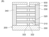
- 9B is a cross-sectional view of a state in which a hard mask 930 is provided on the second film portion 320 of the wafer 200 from the state of FIG. 9A to form a recess 352 in the second film portion 320.
- FIG. 9C is a cross-sectional view of a state in which the hard mask 920 has been removed from the state of FIG. 9B.
- 10 is a cross-sectional view illustrating a step of forming a stopper portion 314 on a first film portion 310 of a wafer 200 in a substrate processing step.
- a processing furnace 202 constituting the substrate processing apparatus 10 has a heater 207 as a temperature regulator (heating unit).
- the heater 207 also functions as an activation mechanism (excitation unit) that activates (excites) a gas by heat.
- a reaction tube 203 is disposed concentrically with the heater 207 inside the heater 207.
- the reaction tube 203 is formed in a cylindrical shape with a closed upper end and an open lower end.
- a manifold 209 is disposed concentrically with the reaction tube 203 below the reaction tube 203.
- An O-ring 220a is provided between the manifold 209 and the reaction tube 203.
- a processing vessel (reaction vessel) is mainly constituted by the reaction tube 203 and the manifold 209.
- a processing chamber 201 is formed in the cylindrical hollow portion of the processing vessel.
- the processing chamber 201 is configured to be capable of containing a wafer 200 as a substrate. Processing of the wafer 200 is carried out in this processing chamber 201.
- Nozzles 249a to 249c serving as first to third supply units are provided in the processing chamber 201, respectively penetrating the side wall of the manifold 209.
- Gas supply pipes 232a to 232c are connected to the nozzles 249a to 249c, respectively.
- Gas supply pipes 232a to 232c are provided with mass flow controllers (MFCs) 241a to 241c, which are flow rate controllers (flow rate control parts), and valves 243a to 243c, which are on-off valves, in order from the upstream side of the gas flow.
- MFCs mass flow controllers
- Gas supply pipes 232d and 232f are connected to gas supply pipe 232a downstream of valve 243a.
- Gas supply pipes 232e and 232g are connected to gas supply pipe 232b downstream of valve 243b.
- Gas supply pipe 232h is connected to gas supply pipe 232c downstream of valve 243c.
- Gas supply pipes 232d to 232h are provided with MFCs 241d to 241h and valves 243d to 243h in order from the upstream side of the gas flow.
- a gas supply pipe 272 is connected to the nozzle 249a.
- the gas supply pipe 272 is provided with, in order from the upstream side of the gas flow, an MFC 271 which is a flow rate controller (flow rate control unit) and a valve 273 which is an on-off valve.
- the aforementioned gas supply pipes 232a, 232d, and 232f are respectively connected to the gas supply pipe 272 downstream of the valve 273.
- the nozzles 249a to 249c are provided in a circular space between the inner wall of the reaction tube 203 and the wafers 200 in a plan view, and are arranged to rise from the bottom to the top of the inner wall of the reaction tube 203 toward the top in the arrangement direction of the wafers 200.
- the nozzles 249a, 249c are arranged to sandwich a straight line L passing through the nozzle 249b and the center of the exhaust port 231a from both sides along the inner wall of the reaction tube 203.
- Gas supply holes 250a to 250c for supplying gas are provided on the side of the nozzles 249a to 249c, respectively.
- the gas supply holes 250a to 250c are each open to face (face) the exhaust port 231a in a plan view, and are capable of supplying gas toward the wafers 200.
- a modifier is supplied into processing chamber 201 via MFC 241a, valve 243a, and nozzle 249a.
- a first raw material is supplied into processing chamber 201 via MFC 241b, valve 243b, and nozzle 249b. The first raw material is used as one of the first film-forming agents.
- a second raw material is supplied into processing chamber 201 via MFC 241e, valve 243e, and nozzle 249b. The second raw material is used as one of the second film-forming agents.
- a reactant is supplied into processing chamber 201 via MFC 241c, valve 243c, and nozzle 249c.
- the reactant is used as one of the film-forming agents.
- a catalyst is supplied into the processing chamber 201 via the MFC 241d, the valve 243d, the gas supply pipe 232a, and the nozzle 249a.
- the catalyst is used as one of the film forming agents.
- an inert gas is supplied into the processing chamber 201 via the MFCs 241f to 241h, the valves 243f to 243h, the gas supply pipes 232a to 232c, and the nozzles 249a to 249c, respectively.
- the inert gas acts as a purge gas, a carrier gas, a dilution gas, etc.
- a remover is supplied into the processing chamber 201 via the MFC 271, the valve 273, and the nozzle 249a.
- the modifying agent supply system is made up of gas supply pipe 232a, MFC 241a, and valve 243a
- the first raw material supply system is made up of gas supply pipe 232b, MFC 241b, and valve 243b
- the second raw material supply system is made up of gas supply pipe 232e, MFC 241e, and valve 243e
- the reactant supply system is made up of gas supply pipe 232c, MFC 241c, and valve 243c
- the catalyst supply system is made up of gas supply pipe 232d, MFC 241d, and valve 243d
- the inert gas supply system is made up of gas supply pipes 232f-232h, MFC 241f-241h, and valves 243f-243h.
- Each or all of the first raw material supply system, second raw material supply system, reactant supply system, and catalyst supply system are also referred to as a film-forming agent supply system.
- the gas supply pipe 272, the MFC 271, and the valve 273 mainly constitute the remover supply system.
- any or all of the various supply systems described above may be configured as an integrated supply system 248 in which valves 243a-243h, 273 and MFCs 241a-241h, 271, etc. are integrated.
- An exhaust port 231a for exhausting the atmosphere in the processing chamber 201 is provided at the bottom of the side wall of the reaction tube 203.
- An exhaust pipe 231 is connected to the exhaust port 231a.
- a vacuum pump 246 is connected to the exhaust pipe 231 via a pressure sensor 245 for detecting the pressure in the processing chamber 201 and an APC (Auto Pressure Controller) valve 244.
- the APC valve 244 can evacuate and stop the vacuum evacuation of the processing chamber 201 by opening and closing the valve while the vacuum pump 246 is operating, and is further configured to adjust the pressure in the processing chamber 201 by adjusting the valve opening based on pressure information detected by the pressure sensor 245.
- An exhaust system is mainly configured by the exhaust pipe 231, the APC valve 244, and the pressure sensor 245.
- the vacuum pump 246 may be included in the exhaust system.
- a seal cap 219 is provided below the manifold 209, which can airtightly close the lower end opening of the manifold 209 via an O-ring 220b.
- a rotation mechanism 267 for rotating the boat 217 is provided below the seal cap 219.
- the rotation shaft 255 of the rotation mechanism 267 is connected to the boat 217.
- the rotation mechanism 267 is configured to rotate the wafers 200 by rotating the boat 217.
- the boat elevator 115 is configured as a transport device that transports the wafers 200 in and out of the processing chamber 201 by raising and lowering the seal cap 219.
- a shutter 219s is provided below the manifold 209 that can airtightly close the lower end opening of the manifold 209 via an O-ring 220c when the seal cap 219 is lowered and the boat 217 is removed from the processing chamber 201.
- the boat 217 which serves as a substrate support, is configured to support multiple wafers 200 (for example, 25 to 200 wafers) in a horizontal position, aligned vertically with their centers aligned, and arranged in multiple stages, i.e., spaced apart.
- heat insulating plates 218 made of a heat-resistant material are supported in multiple stages.
- a temperature sensor 263 is installed inside the reaction tube 203. By adjusting the power supply to the heater 207 based on the temperature information detected by the temperature sensor 263, the temperature inside the processing chamber 201 is distributed as desired.
- the controller 121 which is the control unit, is configured as a computer equipped with a CPU (Central Processing Unit) 121a, a RAM (Random Access Memory) 121b, a storage device 121c, and an I/O port 121d.
- the RAM 121b, the storage device 121c, and the I/O port 121d are configured to be able to exchange data with the CPU 121a via an internal bus 121e.
- An input/output device 122 configured as, for example, a touch panel, is connected to the controller 121.
- an external storage device 123 can be connected to the controller 121.
- the storage device 121c is composed of, for example, a flash memory, a HDD (Hard Disk Drive), an SSD (Solid State Drive), etc.
- a control program for controlling the operation of the substrate processing device, a process recipe describing the procedures and conditions of the substrate processing described later, etc. are readably recorded and stored.
- the process recipe is a combination of procedures in the substrate processing described later that are executed by the controller 121 in the substrate processing device to obtain a predetermined result, and functions as a program.
- at least one of the process recipe and the control program is also simply referred to as a program.
- the process recipe is also simply referred to as a recipe.
- the RAM 121b is configured as a memory area (work area) in which the programs and data read by the CPU 121a are temporarily stored.
- the I/O port 121d is connected to the above-mentioned MFCs 241a to 241h, 271, valves 243a to 243h, 273, pressure sensor 245, APC valve 244, vacuum pump 246, temperature sensor 263, heater 207, rotation mechanism 267, boat elevator 115, etc.
- the CPU 121a is configured to read and execute a control program from the storage device 121c, and to read a recipe from the storage device 121c in response to input of an operation command from the input/output device 122, etc.
- the CPU 121a is configured to control the flow rate adjustment of various substances (various gases) by the MFCs 241a-241h, 271, the opening and closing of the valves 243a-243h, 273, the opening and closing of the APC valve 244 and the pressure adjustment by the APC valve 244 based on the pressure sensor 245, the start and stop of the vacuum pump 246, the temperature adjustment of the heater 207 based on the temperature sensor 263, the rotation and rotation speed adjustment of the boat 217 by the rotation mechanism 267, the raising and lowering of the boat 217 by the boat elevator 115, etc.
- the controller 121 can be configured by installing the above-mentioned program recorded and stored in the external storage device 123 into a computer.
- the external storage device 123 includes, for example, a magnetic disk such as an HDD, an optical disk such as a CD, a magneto-optical disk such as an MO, and a semiconductor memory such as a USB memory or an SSD.
- the storage device 121c and the external storage device 123 are configured as computer-readable recording media. Hereinafter, these will be collectively referred to simply as recording media.
- the program may be provided to the computer using a communication means such as the Internet or a dedicated line, without using the external storage device 123.
- the diagonal lines representing the cross section of the second film portion 320 have been omitted to avoid the diagram becoming too cluttered and difficult to see.
- the portions of the first film portion 310 hidden by the second film portion 320 have been shown as solid lines rather than as hidden dashed lines to avoid the diagram becoming too cluttered and difficult to see.
- the diagonal lines representing the cross section of the second film portion 320 have been omitted.
- the wafer 200 has a first film portion 310, which is generally rod-shaped, on a base material 300, and a second film portion 320 that covers the first film portion 310.
- first film portion and the “second film portion” are sometimes simply referred to as the "first film” and the "second film”.
- the up-down direction of the wafer 200 will be described when it is loaded into the processing furnace 202 (see FIG. 1) of the substrate processing apparatus 10.
- the left-right direction in FIG. 5A is the longitudinal direction of the first film portion 310
- the direction perpendicular to the paper surface of FIG. 5A is the front-rear direction.
- the view from the direction perpendicular to the top surface of the base material 300 is taken as a planar view.
- the first film portion 310 is formed so as to be spaced apart from one another in the front-to-rear direction in plan view. Also, in this embodiment, the first film portion 310 is composed of a plurality of block-shaped (more specifically, rod-shaped) films spaced apart from one another in a direction perpendicular to the longitudinal direction, i.e., in the up-down direction perpendicular to the top surface of the base material 300. From another perspective, the first film portion 310 is formed so that at least a portion of it is embedded in the second film portion 320, and is composed of block-shaped films spaced apart from one another in the up-down and front-to-rear directions.
- the portion composed of the first membrane portion 310 and the second membrane portion 320 is referred to as the main portion 302.
- the left and right sides of the main portion 302 are the surfaces where the sides of the first membrane portion 310 and the second membrane portion 320 are exposed.
- the right side of the main portion 302 in the figure is the side where the end face of the first portion 311A (see FIG. 7D) of the first membrane portion 310 described below and the end face of the second membrane portion 320 are exposed.
- the left side of the main portion 302 in the figure is the side where the end face of the second portion 311B (see FIG. 7D) of the first membrane portion 310 described below and the end face of the second membrane portion 320 are exposed.
- a third film portion 330 is formed on the base material 300 of the wafer 200 so as to be adjacent to and cover one longitudinal side of the first film portion 310 in the main portion 302, in other words, the right side in the left-right direction.
- a fourth film portion 340 is formed on the base material 300 of the wafer 200 so as to be adjacent to and cover the other longitudinal side of the first film portion 310 in the main portion 302, in other words, the left side in the left-right direction. Note that the "third film portion” and “fourth film portion” are sometimes simply referred to as the "third film” and "fourth film”.
- a surface film (not shown) is formed on the surface of the first film portion 310 that comes into contact with the second film portion 320.
- the first film portion 310 will be described below as a silicon film (Si film) that is a non-oxide film (non-oxygen-containing film), the surface film of the first film portion 310 will be described as a SiO film that is a gate insulating film, and the second film portion 320 will be described as a silicon oxide carbon film (SiOC film) that is an oxide film (oxygen-containing film) and a carbonized film (carbon-containing film).
- the third film portion 330 and the fourth film portion 340 will both be described as silicon oxide films (SiO films).
- the base material 300 is preferably formed from a material that is not etched in the pre- and post-processing steps described below, or that has a low etching rate relative to the film to be etched. However, these are representative examples and are not limited to these.
- a step in a manufacturing process of a semiconductor device (a) in a wafer 200 having the above-described structure in which a first film portion 310 and a second film portion 320 covering the first film portion 310 are formed, a step of replacing a part of the portion of the first film portion 310 covered by the second film portion 320 with a stopper portion 314 (see FIG. 7D ) and dividing the first film portion 310 into a first portion 311A and a second portion 311B (see FIG.
- a substrate processing apparatus 10 is used to form a stopper portion 314 in a first film portion 310 formed on a base material 300 of a wafer 200 as a substrate shown in FIG. 5B, thereby dividing the first film portion 310 into a first portion 311A and a second portion 311B.
- the "stopper portion” is sometimes referred to as a "stopper film.”
- an example of a substrate processing process further includes a process that does not use the substrate processing apparatus 10. Specifically, it includes a "pre-process” before forming the stopper portion 314 (see FIG. 7D) on the first film portion 310 of the wafer 200, which will be described later, and a “post-process” after forming the stopper portion 314. These "pre-process” and “post-process” do not use the substrate processing apparatus 10.
- the substrate processing process example is also an example of a substrate processing method and a method for manufacturing a semiconductor device.
- the operation of each part constituting the substrate processing apparatus 10 is controlled by the controller 121.
- pre-process In a pre-process, as shown in FIG. 6B, a groove 350 is formed in the main portion 302 of the wafer 200 shown in FIG. 6A along the front-rear direction in a plan view.
- a hard mask 900 is formed on the upper surface of the wafer 200 opposite the base material 300, and a groove 350 penetrating the first film portion 310 and the second film portion 320 is formed by etching. More specifically, the groove 350 is formed so as to penetrate the second film 320 and a part of the portion of the first film portion 310 that is covered by the second film portion 320.
- the end face of the first film portion 310 exposed in the groove portion 350 is referred to as the first end face 312.
- the end face of the second film portion 320 exposed in the groove portion 350 is referred to as the second end face 322.
- anisotropic etching using a carbon fluoride (CF)-based gas plasma can be used for the etching.
- CF carbon fluoride
- the CF-based gas for example, one or more of CF 4 , C 4 F 6 , C 4 F 8 , CH 2 F 2 , and CHF 3 can be used.
- the etching process in this step can be performed using a known etching device capable of performing an etching process on the wafer 200. The same applies to other etching processes in the following steps.
- a plasma etching device that enables etching having anisotropy in the vertical direction that penetrates the first film portion 310 and the second film portion 320.
- the hard mask 900 is removed.
- the hard mask removal process in this step can be performed using, for example, a known ashing device capable of performing an ashing process on the hard mask on the wafer 200. The same applies to the removal processes of the other hard masks in the subsequent steps.
- the process of forming the stopper portion 314 will be specifically described. Note that in the following description, an example will be described in which, as part of the stopper portion formation process, a removal step of removing the modified layer 324 described below and a second film formation step of backfilling the groove portion 350 with the second film portion 320 are further performed; however, the stopper portion formation process may not include these steps.
- the film-forming agent contains a raw material, a reactant, and a catalyst
- the raw material, the reactant, and the catalyst each have a different molecular structure.
- the specific substance contained in the film-forming agent is a raw material
- the specific substance contained in the film-forming agent may be a reactant. That is, the molecule X may be a reactant molecule.
- the specific substance contained in the film-forming agent may be a catalyst. That is, the molecule X may be a catalyst molecule. That is, the specific substance contained in the film-forming agent may contain at least one of the raw material, the reactant, and the catalyst.
- a cycle including a step of supplying a first raw material to the wafer 200 and a step of supplying a reactant to the wafer 200 is performed a predetermined number of times in the first film formation step, and a catalyst is supplied to the wafer 200 in at least one of the steps of supplying the first raw material and the step of supplying the reactant.
- FIG. 4 shows a typical example in which a catalyst is supplied in both the step of supplying the first raw material and the step of supplying the reactant.
- the first film formation step is a step in which a part of the first film portion 310 is replaced with a stopper portion 314, and the stopper portion 314 divides the first film portion 310 into a first portion 311A and a second portion 311B.
- a catalyst may be supplied to the wafer 200 in at least one of the steps of supplying the first raw material and supplying the reactant.
- Modifier ⁇ (first raw material + catalyst ⁇ reactant) ⁇ n Modifier ⁇ (first raw material ⁇ reactant + catalyst) ⁇ n Modifier ⁇ (first raw material + catalyst ⁇ reactant + catalyst) ⁇ n
- wafer used in this specification can mean the wafer itself, or a laminate of the wafer and a specified layer or film formed on its surface.
- surface of a wafer used in this specification can mean the surface of the wafer itself, or the surface of a specified layer, etc. formed on the wafer.
- agent as used in this specification includes at least one of gaseous substances and liquid substances.
- Liquid substances include mist-like substances.
- an inhibitor layer includes at least one of a continuous layer and a discontinuous layer.
- an inhibitor layer may include a continuous layer, a discontinuous layer, or both, so long as it is capable of producing a film formation inhibitory effect.
- the inside of the processing chamber 201 i.e., the space in which the wafers 200 are present, is evacuated (reduced pressure exhaust) by the vacuum pump 246 so that the inside of the processing chamber 201 is at a desired pressure (vacuum level).
- the pressure inside the processing chamber 201 is measured by the pressure sensor 245, and the APC valve 244 is feedback-controlled based on the measured pressure information.
- the wafers 200 in the processing chamber 201 are heated by the heater 207 so that the processing temperature is at a desired processing temperature.
- the power supply to the heater 207 is feedback-controlled based on the temperature information detected by the temperature sensor 263 so that the inside of the processing chamber 201 has a desired temperature distribution.
- the rotation mechanism 267 starts rotating the wafers 200. The evacuation inside the processing chamber 201 and the heating and rotation of the wafers 200 are all continued at least until the processing of the wafers 200 is completed.
- Modification step 7A a modifying agent is supplied to the wafer 200, and a modified layer 324 is formed on the second end surface 322 of the second film portion 320, which is a SiOC film exposed in the groove portion 350. That is, a modifying agent that reacts with the second end surface 322 exposed in the groove portion 350 of the wafer 200 is supplied, and the modified layer 324 is selectively formed on the second end surface 322.
- valve 243a of the substrate processing apparatus 10 shown in FIG. 1 is opened, and the modifying agent is allowed to flow into the gas supply pipe 232a.
- the flow rate of the modifying agent is adjusted by the MFC 241a, and the modifying agent is supplied into the processing chamber 201 via the nozzle 249a, and exhausted from the exhaust port 231a.
- the modifying agent is supplied to the wafer 200 from the side of the wafer 200 (modifying agent supply).
- the valves 243f to 243h may be opened, and an inert gas may be supplied into the processing chamber 201 via each of the nozzles 249a to 249c.
- the modified layer 324 shown in FIG. 7A is an inhibitor layer.
- the inhibitor molecules which are at least a part of the molecular structure of the molecules constituting the modifier, can be chemically adsorbed to the second end surface 322 exposed in the groove portion 350 of the wafer 200, and the second end surface 322 can be modified to form the modified layer 324, which is an inhibitor layer. That is, in this step, by supplying a modifier that reacts with the second end surface 322 to the wafer 200, the second end surface 322 can be modified so that the inhibitor molecules contained in the modifier are adsorbed to the second end surface 322 to form the modified layer 324.
- the inhibitor molecules are also referred to as film formation inhibitor molecules (adsorption inhibitor molecules, reaction inhibitor molecules).
- the modified layer 324 is also referred to as a film formation inhibitor layer (adsorption inhibitor layer, reaction inhibitor layer).
- the modified layer 324 formed in this step contains at least a portion of the molecular structure of the molecules that make up the modifier, which is a residue derived from the modifier.
- the modified layer 324 prevents at least a portion of the molecular structure of the molecules that make up the first raw material (film-forming agent) from adsorbing to the first end surface 312 in the first film-forming step described below, and inhibits (suppresses) the progress of the film-forming reaction at the first end surface 312.
- At least a part of the molecular structure of the molecule constituting the modifier, i.e., the inhibitor molecule, is exemplified by trialkylsilyl groups such as trimethylsilyl group (-SiMe 3 ) and triethylsilyl group (-SiEt 3 ).
- the trialkylsilyl group contains an alkyl group, i.e., a hydrocarbon group.
- Si of the trimethylsilyl group or triethylsilyl group is adsorbed to an adsorption site on the second end surface 322 of the wafer 200.
- the second end surface 322 When the second end surface 322 is the surface of a SiOC film, the second end surface 322 contains an OH termination (OH group) as an adsorption site, and Si of the trimethylsilyl group or triethylsilyl group is bonded to O of the OH termination (OH group) on the second end surface 322, so that the second end surface 322 is terminated by an alkyl group such as a methyl group or an ethyl group, i.e., a hydrocarbon group.
- OH group OH termination
- the alkyl group such as a methyl group (trimethylsilyl group) or an ethyl group (triethylsilyl group), i.e., a hydrocarbon group, which terminates second end face 322, constitutes an inhibitor layer and prevents at least a portion of the molecular structure of the molecules that constitute the first raw material (film-forming agent) from being adsorbed to second end face 322 in the second film-forming step described below, thereby inhibiting (suppressing) the progress of the film-forming reaction at second end face 322.
- the molecular structure of the molecules constituting the modifier may be adsorbed to a part of the first end surface 312 of the first film portion 310, which is the Si film of the wafer 200, but the amount of adsorption is small, and the amount of adsorption to the second end surface 322 of the wafer 200 is overwhelmingly greater.
- Such selective (preferential) adsorption is possible because the processing conditions in this step are set to conditions in which the modifier does not undergo gas phase decomposition within the processing chamber 201. Also, this is because the second end surface 32 is OH-terminated over its entire area, whereas most of the area of the first end surface 312 is not OH-terminated.
- the modifier does not undergo gas-phase decomposition in the processing chamber 201 (see FIG. 1), at least a portion of the molecular structure of the molecules that make up the modifier is not deposited in multiple layers on the first end face 312 and the second end face 322, and at least a portion of the molecular structure of the molecules that make up the modifier is selectively adsorbed to the second end face 322 out of the first end face 312 and the second end face 322, so that the second end face 322 is selectively terminated by at least a portion of the molecular structure of the molecules that make up the modifier.
- the processing conditions for supplying the modifying agent in the modification step are as follows: Treatment temperature: room temperature (25°C) to 500°C, preferably room temperature to 250°C Treatment pressure: 5 to 2000 Pa, preferably 10 to 1000 Pa Treatment time: 1 second to 120 minutes, preferably 30 seconds to 60 minutes Modifier supply flow rate: 0.001 to 3 slm, preferably 0.001 to 0.5 slm Inert gas supply flow rate (per gas supply pipe): 0 to 20 slm Examples are given below.
- 0 slm means that the substance (gas) is not being supplied. This also applies to the following explanations.
- the processing temperature refers to the temperature of the wafer 200 or the temperature inside the processing chamber 201
- the processing pressure refers to the pressure inside the processing chamber 201
- the processing time refers to the time the processing continues.
- valve 243a shown in FIG. 1 is closed to stop the supply of the modifying agent into the processing chamber 201. Gaseous substances remaining in the processing chamber 201 are removed from the processing chamber 201 (purging). Note that the processing temperature when purging in this step is preferably the same as the processing temperature when the modifying agent is supplied.
- modifiers examples include compounds having a structure in which an amino group is directly bonded to silicon (Si), and compounds having a structure in which an amino group and an alkyl group are directly bonded to silicon (Si).
- the modifier examples include (dimethylamino)trimethylsilane (( CH3 ) 2NSi ( CH3 ) 3 ), (diethylamino)triethylsilane (( C2H5 )2NSi ( C2H5 )3), (dimethylamino)triethylsilane (( CH3 ) 2NSi ( C2H5 ) 3 ), (diethylamino)trimethylsilane ((C2H5 ) 2NSi(CH3)3), (dipropylamino)trimethylsilane ((C3H7 ) 2NSi ( CH3 ) 3 ) , (dibutylamino)trimethylsilane ((C4H9)2NSi(CH3)3 ) , ( trimethylsilyl ) amine ( ( CH3 ) 3SiNH2 ), ( triethylsilyl )amine ((C 2H5 ) 3SiNH2 ), ( dimethyla
- the modifier examples include bis(dimethylamino)dimethylsilane ([( CH3 ) 2N ] 2Si ( CH3 ) 2 ), bis(diethylamino)diethylsilane ([ ( C2H5 ) 2N ] 2Si ( C2H5 ) 2 ) , bis(dimethylamino)diethylsilane ([(CH3) 2N ] 2Si ( C2H5 ) 2 ) , bis(diethylamino)dimethylsilane ([ ( C2H5 ) 2N ] 2Si ( CH3 ) 2 ), bis(dimethylamino) silane ([ ( CH3) 2N ] 2SiH2 ), bis(diethylamino)silane ([( C2H5 ) 2N ] 2SiH2 ) , bis(dimethylaminodimethylsilyl)ethane ([( CH3 ) 2N ( CH
- a first film forming agent is supplied to the groove 350 of the wafer 200 to form a first stopper portion 314 on the first end surface 312 of the first film portion 310, which is a Si film exposed in the groove 350 of the wafer 200.
- a first source material that reacts with the first end surface 312 is supplied to the groove 350 of the wafer 200 to selectively adsorb at least a part of the molecular structure of the molecules that constitute the first source material onto the first end surface 312.
- the adsorption layer formed by adsorption is reacted with a reactant to form at least a part of the stopper portion 314 (i.e., deposited). More specifically, the stopper portion 314 is deposited from each of the first end surfaces 312 on both sides exposed to the groove 350, in other words, grown to fill the gap between the first end surfaces 312.
- the stopper portion 314 in the first membrane portion 310 is referred to as the first portion 311A, and the other side is referred to as the second portion 311B.
- the stopper portion 314 is formed so as to fill the space between the first end faces 312 of the first membrane portion 310, resulting in a configuration in which a part of the first membrane portion 310 is replaced with the stopper portion 314.
- the stopper portion 314 divides the first membrane portion 310 into the first portion 311A and the second portion 311B.
- the stopper portion 314 and the second film portion 320 have different compositions.
- the stopper portion 314 is a silicon oxide film (SiO film). That is, the first film formation step is, as an example, the selective formation of a SiO film using a halogen-containing Si source.
- the first film-forming agent includes a first raw material, a reactant, and a catalyst.
- the output of the heater 207 is adjusted to maintain the temperature of the wafer 200 at or below the temperature of the wafer 200 in the modification step.
- the time required to change the temperature of the wafer 200 can be omitted, and the processing time can be shortened.
- a temperature lower than the temperature of the wafer 200 in the modification step it is possible to more effectively suppress the detachment of at least a portion of the modified layer 324.
- a first source material (first source gas) and a catalyst (catalytic gas) are supplied to the groove portion 350 as a first film-forming agent on the wafer 200 after the modification step has been performed, i.e., the wafer 200 after a modified layer 324 has been selectively formed on the second end surface 322 of the second film portion 320, and a first layer is formed on the first end surface 312 exposed in the groove portion 350.
- the first layer formed in this step is in a state prior to oxidation in the reactant supply step described below.
- the valves 243b and 243d of the substrate processing apparatus 10 shown in FIG. 1 are opened, and the first raw material, which is the first film forming agent, and the catalyst are respectively flowed into the gas supply pipes 232b and 232d.
- the flow rates of the first raw material and the catalyst are adjusted by the MFCs 241b and 241d, respectively, and the first raw material and the catalyst are supplied into the processing chamber 201 via the nozzles 249b and 249a, mixed in the processing chamber 201, and exhausted from the exhaust port 231a.
- the first raw material and the catalyst are supplied to the wafer 200 from the side of the wafer 200 (supply of the first raw material + catalyst).
- the valves 243f to 243h may be opened to supply an inert gas into the processing chamber 201 via the nozzles 249a to 249c, respectively.
- the first raw material and catalyst By supplying the first raw material and catalyst to the wafer 200 under processing conditions described below, it is possible to selectively chemically adsorb at least a portion of the molecular structure of the molecules that make up the first raw material onto the first end surface 312 while suppressing chemical adsorption of at least a portion of the molecular structure of the molecules that make up the first raw material onto the second film portion 320. As a result, a first layer is formed on the first end surface 312 of the wafer 200.
- the first layer includes at least a portion of the molecular structure of the molecules that make up the first raw material, which is a residue of the first raw material. In other words, the first layer includes at least a portion of the atoms that make up the first raw material.
- the above reaction can be carried out in a non-plasma atmosphere and under low temperature conditions as described below.
- a non-plasma atmosphere and under low temperature conditions as described below, it is possible to maintain the molecules and atoms that make up the modified layer 324 formed on the second end surface 322 without disappearing (detaching) from the second end surface 322.
- the first layer in a non-plasma atmosphere and under low temperature conditions as described below, it is possible to prevent the first raw material from thermally decomposing (vapor phase decomposition), i.e., self-decomposing, in the processing chamber 201.
- thermally decomposing vapor phase decomposition
- This makes it possible to prevent multiple deposition of at least a portion of the molecular structure of the molecules constituting the first raw material on the first end surface 312 and the second end surface 322, and allows at least a portion of the molecular structure of the molecules constituting the first raw material to be selectively adsorbed to the first end surface 312.
- the processing conditions in this step are low temperature conditions, as described below, and conditions under which the first raw material does not decompose in the gas phase in the processing chamber 201. Also, this is because a modified layer 324 is formed on the second end surface 322, while a modified layer 324 is not formed in most areas of the first end surface 312.
- the processing conditions for supplying the first raw material and the catalyst in the raw material supply step are as follows: Treatment temperature: room temperature (25°C) to 200°C, preferably room temperature to 150°C Processing pressure: 133 to 1333 Pa First raw material supply flow rate: 0.001 to 2 slm Catalyst supply flow rate: 0.001 to 2 slm Inert gas supply flow rate (per gas supply pipe): 0 to 20 slm
- the supply time of each gas is, for example, 1 to 120 seconds, preferably 1 to 60 seconds.
- the valves 243b and 243d are closed to stop the supply of the first raw material and catalyst into the processing chamber 201. Then, gaseous substances remaining in the processing chamber 201 are removed from the processing chamber 201 (purging) using the same processing procedure and processing conditions as the purging in the modification step. Note that the processing temperature when purging in this step is preferably the same as the processing temperature when the first raw material and catalyst are supplied.
- a gas containing Si and a halogen can be used as the first raw material.
- the halogen includes chlorine (Cl), fluorine (F), bromine (Br), and iodine (I).
- the Si- and halogen-containing gas preferably contains the halogen in the form of a chemical bond between Si and the halogen.
- a chlorosilane-based gas can be used as the Si- and halogen-containing gas.
- the Si- and halogen-containing gas may further contain O, and preferably contains O in the form of a siloxane bond (Si-O-Si bond).
- a chlorosiloxane-based gas can be used as the Si- and halogen-containing gas. Both of these gases preferably contain Cl in the form of a Si-Cl bond.
- an amino group-containing gas such as an aminosilane-based gas can also be used as the first raw material.
- the first raw material for example, tetrachlorosilane (SiCl 4 ), hexachlorodisilane (Si 2 Cl 6 ), octachlorotrisilane (Si 3 Cl 8 ), etc. can be used.
- the first raw material for example, hexachlorodisiloxane (Cl 3 Si—O—SiCl 3 ), octachlorotrisiloxane (Cl 3 Si—O—SiCl 2 —O—SiCl 3 ), etc.
- the first raw material one or more of these can be used.
- the first raw material for example, tetrakis(dimethylamino)silane (Si[N( CH3 ) 2 ] 4 ), tris(dimethylamino)silane (Si[N( CH3 ) 2 ] 3H ), bis( diethylamino ) silane (Si[N( C2H5 ) 2 ] 2H2 ), bis(tertiarybutylamino)silane ( SiH2 [ NH( C4H9 )] 2 ), and (diisopropylamino)silane ( SiH3 [N( C3H7 ) 2 ]) can be used.
- the first raw material one or more of these can be used .
- an amine-based gas containing carbon (C), nitrogen ( N), and hydrogen (H) can be used.
- a cyclic amine-based gas or a chain amine-based gas can be used.
- a cyclic amine such as pyridine (C5H5N ) , aminopyridine ( C5H6N2 ) , picoline ( C6H7N ), lutidine ( C7H9N ) , pyrimidine ( C4H4N2 ), quinoline ( C9H7N ), piperazine ( C4H10N2 ) , piperidine ( C5H11N ) , aniline ( C6H7N ) can be used.
- a chain amine such as triethylamine ((C2H5)3N), diethylamine ((C2H5)2NH ) , monoethylamine ( ( C2H5 ) NH2 ), trimethylamine ((CH3) 3N ), dimethylamine (( CH3 ) 2NH ), and monomethylamine (( CH3 ) NH2 ) can be used.
- a chain amine such as triethylamine ((C2H5)3N), diethylamine ((C2H5)2NH ) , monoethylamine ( ( C2H5 ) NH2 ), trimethylamine ((CH3) 3N ), dimethylamine (( CH3 ) 2NH ), and monomethylamine (( CH3 ) NH2 )
- the catalyst one or more of these can be used. This also applies to the reactant supply step described below.
- a reactant (reactant gas) and a catalyst (catalyst gas) are supplied as a first film forming agent to the wafer 200, i.e., the wafer 200 on which the first layer has been selectively formed.
- oxidant oxidant gas
- valves 243c and 243d are opened to allow reactants and catalyst to flow into gas supply pipes 232c and 232d, respectively.
- the reactants and catalyst are adjusted in flow rate by MFCs 241c and 241d, respectively, and supplied into processing chamber 201 via nozzles 249c and 249a, mixed in processing chamber 201, and exhausted from exhaust port 231a.
- reactants and catalyst are supplied to wafer 200 from the side of wafer 200 (reactant + catalyst supply).
- valves 243f to 243h may be opened to supply inert gas into processing chamber 201 via nozzles 249a to 249c, respectively.
- the wafer 200 By supplying a reactant and a catalyst to the wafer 200 under processing conditions described below, at least a portion of the first layer formed in the raw material supply step is oxidized. This results in the formation of a second layer, which is the oxidized first layer.
- the above-mentioned reaction can be carried out in a non-plasma atmosphere and under low temperature conditions as described below.
- the molecules and atoms that make up the modified layer 324 formed on the second end surface 322 can be maintained without disappearing (detaching) from the second end surface 322.
- the process conditions for supplying the reactants and catalyst in the reactant supply step are as follows: Treatment temperature: room temperature (25°C) to 200°C, preferably room temperature to 150°C Processing pressure: 133 to 1333 Pa Reactant supply flow rate: 0.001-2 slm Catalyst supply flow rate: 0.001 to 2 slm Inert gas supply flow rate (per gas supply pipe): 0 to 20 slm
- the gas supply time is, for example, 1 to 120 seconds, preferably 1 to 60 seconds.
- valves 243c and 243d are closed to stop the supply of reactants and catalyst into the processing chamber 201. Then, gaseous substances remaining in the processing chamber 201 are removed from the processing chamber 201 (purging) using the same processing procedure and conditions as the purging in the above-mentioned reforming step. Note that the processing temperature when purging in this step is preferably the same as the processing temperature when supplying the reactants and catalyst.
- the reactant i.e., the oxidizing agent
- oxygen (O) and hydrogen (H) containing gas can be used.
- the O and H containing gas for example, water vapor ( H2O gas), hydrogen peroxide ( H2O2 ) gas, hydrogen ( H2 ) gas + oxygen ( O2 ) gas, and H2 gas + ozone ( O3 ) gas can be used. That is, as the O and H containing gas, O containing gas + H containing gas can also be used. In this case, deuterium ( D2 ) gas can also be used as the H containing gas instead of H2 gas. As the reactant, one or more of these can be used.
- H2 gas + O2 gas means a mixed gas of H2 gas and O2 gas.
- the two gases may be mixed (premixed) in a supply pipe and then supplied into the processing chamber 201, or the two gases may be separately supplied into the processing chamber 201 from different supply pipes and mixed (postmixed) in the processing chamber 201.
- an O-containing gas can be used as the reactant, i.e., the oxidizing agent, in addition to the O- and H-containing gas.
- an O-containing gas for example, O2 gas, O3 gas, nitrous oxide ( N2O ) gas, nitric oxide (NO) gas, nitrogen dioxide ( NO2 ) gas, carbon monoxide (CO) gas, and carbon dioxide ( CO2 ) gas can be used.
- the reactant, i.e., the oxidizing agent in addition to these, the various aqueous solutions and various cleaning solutions described above can also be used. In this case, by exposing the wafer 200 to the cleaning solution, the object to be oxidized on the surface of the wafer 200 can be oxidized.
- the reactant one or more of these can be used.
- a catalyst for example, the same catalysts as those exemplified in the raw material supply step described above can be used.
- a film as a stopper portion 314 can be selectively (preferentially) formed on the first end surface 312 of the first film portion 310 of the wafer 200 as shown in FIG. 7B.
- a SiO film as a stopper portion can be selectively grown on the first end surface 312.
- the above-mentioned cycle is repeated multiple times until the stopper portions 314 growing from each of the first end surfaces 312 on both sides exposed to the groove portion 350 fill the gap between the first end surfaces 312. As a result, the stopper portions 314 are formed so as to fill the gap between the first end surfaces 312.
- a remover is supplied to the wafer 200 to remove the modified layer 324 formed on the second end surface 322 of the second film portion 320 exposed in the groove portion 350. That is, a remover that reacts with the modified layer 324, which is an inhibitor layer formed on the second end surface 322 of the wafer 200, is supplied to selectively remove the modified layer 324.
- valve 273 is opened to allow the remover to flow into the gas supply pipe 272.
- the remover is supplied into the processing chamber 201 via the nozzle 249a with the flow rate adjusted by the MFC 271, and is exhausted from the exhaust port 231a. At this time, the remover is supplied to the wafer 200 from the side of the wafer 200 (removal agent supply).
- the modified layer 324 formed on the second end face 322 can be removed by supplying a remover to the wafer 200 under predetermined processing conditions (e.g., 500° C. or higher).
- the modifying agent can be one or more of O3 gas plasma, O2 gas plasma, and an annealing agent.
- a second film forming agent is supplied to the wafer 200, and a film having a different composition from the stopper portion 314 and the same composition as the second film portion 320 is formed in the groove portion 350 of the second film portion 320 of the wafer 200, thereby backfilling the groove portion 350.
- a film having the same composition as the second film portion 320 i.e., a SiOC film
- the present disclosure is not limited thereto.
- any film having a composition that is not etched when removing the third film portion 330, the first part 311A of the first film portion 310, and the stopper portion 314 can be used as a film for backfilling the groove portion 350.
- a film containing O and C can be suitably used.
- a film having the same composition as the second film section 320 is formed by the same procedure as in the first film formation step described above, except that the raw materials supplied are different. That is, a film is formed using a second raw material (second raw material gas), a catalyst, and a reactant as the second film forming agent. Specifically, in the second film formation step, a SiOC film is formed using a Si raw material containing C and halogen, which is a second raw material different from the first raw material.
- the second raw material gas is supplied into the processing chamber 201 through the nozzle 249b by controlling the MFC 241e and the valve 243e in the second raw material gas supply system.
- a gas containing Si, C and a halogen can be used as the second raw material.
- the gas containing Si, C and a halogen preferably contains C in the form of a Si-C bond.
- an alkylenechlorosilane gas containing an alkylene group can be used as the gas containing Si, C and a halogen.
- the alkylene group includes a methylene group, an ethylene group, a propylene group, a butylene group, etc.
- an alkylchlorosilane gas containing an alkyl group can be used as the gas containing Si, C and a halogen.
- the alkyl group includes a methyl group, an ethyl group, a propyl group, a butyl group, etc.
- the second source may be, for example, bis(trichlorosilyl)methane ((SiCl 3 ) 2 CH 2 ), 1,2-bis(trichlorosilyl)ethane ((SiCl 3 ) 2 C 2 H 4 ), 1,1,2,2-tetrachloro-1,2-dimethyldisilane ((CH 3 ) 2 Si 2 Cl 4 ), 1,2-dichloro-1,1,2,2-tetramethyldisilane ((CH 3 ) 4 Si 2 Cl 2 ), and 1,1,3,3-tetrachloro-1,3-disilacyclobutane (C 2 H 4 Cl 4 Si 2 ).
- One or more of these may be used as the second source.
- An example of a processing sequence of the film formation process in this step is as follows: (second material + catalyst ⁇ reactant + catalyst) x n
- a cycle including a source supply step of supplying the second source and the catalyst to the wafer 200 and a reactant supply step of supplying the reactant and the catalyst to the wafer 200 is repeated multiple times until the groove portion 350 is filled with a film formed by this cycle.
- the modified layer 324 when backfilling the groove portion 350 with the second film portion 320 in this step, in the case of performing mild film formation such as not using plasma, it is desirable to perform the above-mentioned removal step of the modified layer 324 before backfilling.
- a film formation method using plasma in this step for example, when using a plasma-excited gas such as O2 plasma as a reactant, when using a gas with a high energy state such as O3 , and when this step is performed with the temperature of the wafer 200 being, for example, 300°C or higher (400°C or higher as an example where the effect is more pronounced), the modified layer 324 may not act as a film formation inhibiting layer, and the above-mentioned removal step may be omitted.
- an inert gas serving as a purge gas is supplied into the processing chamber 201 from each of the nozzles 249a to 249c of the substrate processing apparatus 10 shown in FIG. 1 and exhausted from the exhaust port 231a. This causes the processing chamber 201 to be purged, and gases and reaction by-products remaining in the processing chamber 201 are removed from the processing chamber 201. Thereafter, the atmosphere in the processing chamber 201 is replaced with the inert gas, and the pressure in the processing chamber 201 is returned to normal pressure.
- the seal cap 219 is lowered by the boat elevator 115 to open the lower end of the manifold 209. Then, the processed wafers 200 are supported by the boat 217 and unloaded from the lower end of the manifold 209 to the outside of the reaction tube 203 (boat unloading). After being unloaded to the outside of the reaction tube 203, the processed wafers 200 are taken out of the boat 217.
- the modification step and the first film formation step in the same processing chamber (in-situ). This allows the modification step and the first film formation step to be performed without exposing the wafer 200 to the atmosphere, and selective growth can be performed appropriately. In other words, by performing these steps in the same processing chamber, selective growth can be performed with high selectivity. Furthermore, if the removal step can be omitted as described above, the time required to load and unload the wafer 200 can be saved by performing the modification step, the first film formation step, and the second film formation step in the same processing chamber.
- a hard mask 910 is formed on the upper surface of the wafer 200 so as to cover at least the fourth film portion 340, and the third film portion 330 is removed by etching.
- etching anisotropic etching using carbon fluoride (CF)-based gas plasma can be used, for example, as in the previous process. Note that anisotropic etching does not have to be used.
- CF carbon fluoride
- first portion 311A of first film portion 310 is removed by etching down to stopper portion 314.
- first portion 311A is removed by etching from the side surface where first portion 311A is exposed down to stopper portion 314.
- first portion 311A is removed from the end surface not covered by second film portion 320 down to stopper portion 314.
- the stopper portion 314 prevents the second portion 311B of the first film portion 310 from being etched.
- etching gas used to etch the first film portion 310, which is a Si film
- a fluorine (F)-based gas and a chlorine (Cl)-based gas can be used.
- fluorine (F 2 ) gas, chlorine (Cl 2 ) gas, and chlorine trifluoride (ClF 3 ) gas can be used.
- a gas e.g., hydrogen fluoride (HF) gas, etc.
- HF hydrogen fluoride
- a hard mask 920 is formed so as to cover at least the fourth film portion 340, and the stopper portion 314 of the first film portion 310 is removed by etching.
- the etching selectively removes the stopper portion 314, which is a SiO film, so as to leave the second portion 311B of the first film portion 310, which is a Si film, and the second film portion 320, which is a SiOC film.
- the etching method may be wet etching or dry etching using an etching agent containing fluorine (F).
- F fluorine
- the etching agent for example, an aqueous solution or gas containing hydrogen fluoride (HF) may be used.
- the hard mask 920 is removed as shown in FIG. 8D.
- etching processes in the post-processing steps may each be performed using a different etching device, or multiple processes may be performed using the same etching device.
- a stopper portion 314 is formed in a portion of the first film portion 310 of the wafer 200, the first film portion 310 is divided into a first portion 311A and a second portion 311B, and the first portion 311A is removed down to the stopper portion 314.
- a portion of the first film portion 310 i.e., the first portion 311A, can be removed with precision, leaving the second portion 311B.
- a groove 350 is formed in the wafer 200 penetrating the first film portion 310 and the second film portion 320, a first raw material (first film forming agent) is supplied into the groove 350, and at least a part of the molecular structure of the molecules that make up the raw material is selectively deposited on the first end surface 312 of the first film portion 310 exposed in the groove 350, thereby forming a stopper portion 314. Therefore, even if the first film portion 310 is covered with the second film portion 320, the stopper portion 314 can be formed at a desired position of the first film portion 310.
- first raw material first film forming agent
- a modified layer 324 that inhibits adsorption of the first raw material is selectively formed on the second end surface 322 of the second film portion 320 exposed in the groove portion 350. This makes it possible to suppress or prevent the formation of a stopper portion 314 on the second end surface 322 of the second film portion 320.
- the modified layer 324 exposed in the groove portion 350 is removed, and then the second film portion 320 is formed in the groove portion 350 to backfill it. This makes it possible to avoid the modified layer 324 hindering the backfilling of the second film portion 320.
- the stopper portion 314 is removed to leave the second portion 311B. This allows the second portion 311B of the first film portion 310 to be left with high precision.
- the periphery of the first film portion 310 is covered with the second film portion 320. Furthermore, the other end face of the second portion 311B of the first film portion 310 is covered with the fourth film portion 340. Therefore, when etching the first part 311A and the stopper portion 314 of the first film portion 310, the second film portion 320 can prevent the circumferential surface perpendicular to the longitudinal direction of the first film portion 310 from being etched, and the fourth film portion 340 can prevent the other end face of the second portion 311B from being etched.
- a plurality of first film portions 310 are formed at intervals within the second film portion 320. Therefore, by forming the groove portion 350 in the wafer 200, the stopper portion 314 can be formed at the same position of the plurality of first film portions 310.
- the stopper portions 314 in the same position on the first film portion 310 of the wafer 200 in this manner, the first portions 311A of the multiple first film portions 310 can each be removed in the same manner. Similarly, the second portions 311B of the multiple first film portions 310 can each be left aligned in the same manner.
- the first film portion 310 of the wafer 200 is an oxygen-free film
- the second film portion 320 is an oxygen-containing film. Therefore, the OH termination density of the second end surface 322 of the second film portion 320, which is an oxygen-containing film, can be made greater than the OH termination density of the first end surface 312 of the first film portion 310, which is an oxygen-free film. Therefore, the modifying agent can be selectively reacted with and adsorbed onto the OH groups of the second end surface 322 of the second film portion 320 exposed in the groove portion 350, making it easy to selectively form the modified layer 324.
- the stopper portion 314 of the wafer 200 is an oxygen-containing film. Therefore, when the first portion 311A of the first film portion 310, which is a non-oxygen-containing film, is removed by etching, it can function as an etching stopper film against an etching agent that has the effect of etching non-oxygen-containing films.
- the first film portion 310 of the wafer 200 is made of a Si film
- the stopper portion 314 is made of a SiO film
- the second film portion 320 is made of a SiOC film.
- a cycle of alternating between a raw material supply step and a reactant supply step is performed a predetermined number of times, and a catalyst is supplied to the wafer 200 in at least one of the raw material supply step and the reactant supply step, thereby enabling selective growth to be performed with good controllability under the low temperature conditions described above.
- a recess 352 is formed in the second film portion 320 of the wafer 200 shown in FIG. 9A so that a part of the first film portion 310 is exposed.
- a hard mask 930 is formed on the upper surface of the wafer 200, and the second film portion 320 is selectively removed by etching so that the first film portion 310 remains, to form the recess 352.
- etching method for example, dry etching performed by supplying an etching gas to the wafer 200 can be used.
- anisotropic etching using gas plasma can be preferably used.
- etching gas for example, a gas containing a halogen element, C and H (hydrogen) can be used.
- a gas containing a halogen element, C and H hydrogen
- one or more of hydrofluorocarbon (CHF 2 ) gas and hydrochlorofluorocarbon (CHClF 2 ) gas, which are fluorocarbons containing H can be used.
- a mixed gas of a CF-based gas such as carbon tetrafluoride (CF 4 ) gas and an H-containing gas such as H 2 gas can be used.
- the hard mask 930 is removed.
- a second modifier is supplied to the wafer 200, and the portion of the first film portion 310 exposed to the recess 352 is modified by the second modifier.
- the portion of the first film portion 310 modified by the second modifier constitutes the stopper portion 314 (modification process).
- a substrate processing apparatus having a similar configuration to the substrate processing apparatus 10 and including a second modifier supply system that supplies the second modifier instead of the modifier supply system can be used.
- first portion 311A One side of the stopper portion 314 in the first membrane portion 310 is referred to as the first portion 311A, and the other side is referred to as the second portion 311B.
- first membrane portion 310 is configured such that a portion thereof has been modified and replaced with the stopper portion 314.
- the stopper portion 314 divides the first membrane portion 310 into the first portion 311A and the second portion 311B.
- the second modifier is an oxidizing agent
- the stopper portion 314 is an oxide film, as in the above embodiment.
- the oxidation rate of the first film portion 310, which is a Si film, by the oxidizing agent is greater than the oxidation rate of the second film portion 320, which is a SiOC film.
- the portion of the first film portion 310 exposed to the recess 352 is selectively oxidized, and the stopper portion 314 is formed.
- the subsequent steps are the same as in the embodiment described above. Specifically, the steps after the second film formation step and the subsequent steps are the same as in the embodiment described above.
- the stopper portion 314 can be formed by modifying the portion of the first film portion 310 exposed to the recess 352, thereby simplifying the process.
- the wafer 200 includes a second film forming step of backfilling the groove 350 or the recess 352 with the second film portion 320.
- the wafer 200 does not necessarily have to include the second film forming step.
- the first film portion 310 in the wafer 200 may be an oxygen-free film other than a Si film, such as a silicon nitride film (SiN film) or a metal-containing film.
- the second film portion 320 in the wafer 200 may be an oxygen-containing film other than a SiOC film, such as a SiO film, a silicon carbonitride film (SiOCN film), or a metal oxide film.
- the wafer 200 may have multiple types of regions made of different materials as the first film portion 310. Furthermore, the wafer 200 may have multiple types of regions made of different materials as the second film portion 320.
- the first film portion 310 and the second film portion 320 in the wafer 200 can be selected from a group including semiconductor-containing films such as silicon oxycarbonitride film (SiOCN film), silicon oxycarbonide film (SiOC film), silicon oxynitride film (SiON film), silicon carbonitride film (SiCN film), silicon carbide film (SiC film), silicon borocarbonitride film (SiBCN film), silicon boronitride film (SiBN film), silicon borocarbide film (SiBC film), silicon film (Si film), germanium film (Ge film), silicon germanium film (SiGe film), metal-containing films such as titanium nitride film (TiN film), tungsten film (W film), molybdenum film (Mo film), ruthenium film (Ru film), cobalt film (Co film), nickel film (Ni film), copper film (Cu film), amorphous carbon film (a-C film), and single crystal Si (Si wafer).
- the stopper portion 314 may be formed with a semiconductor-containing film such as a SiON film, a SiOCN film, a SiCN film, a SiC film, a SiN film, a SiBCN film, a SiBN film, a SiBC film, a Si film, a Ge film, or a SiGe film, or a metal-containing film such as a TiN film, a W film, a WN film, a Mo film, a Ru film, a Co film, a Ni film, an Al film, an AlN film, a TiO film, a WO film, a WON film, a MoO film, a RuO film, a CoO film, a NiO film, an AlO film, a ZrO film, a HfO film, or a TaO film.
- a semiconductor-containing film such as a SiON film, a SiOCN film, a SiCN film, a SiC film, a SiN film, a SiB
- a film having a composition that is relatively etch-resistant to the etching agent used when etching the first portion 311A of the first film portion 310 is selected.
- a film having a composition that is relatively etch-resistant to the etching agent used when etching the stopper portion 314 ... easier to form a modified layer (inhibitor layer) on the surface of the second film portion 320 than on the surface of the first film portion 310 can be selected from a combination of films having a composition that makes it relatively easier to form a modified layer (inhibitor layer) on the surface of the second film portion 320 than on the surface of the first film portion 310.
- the recipes used for each process are prepared individually according to the process content, and are recorded and stored in the storage device 121c via a telecommunications line or the external storage device 123. Then, when starting each process, it is preferable that the CPU 121a appropriately selects an appropriate recipe according to the process content from among the multiple recipes recorded and stored in the storage device 121c.
- an example of forming a film using a batch-type substrate processing apparatus that processes multiple substrates at a time has been described.
- the present disclosure is not limited to the above embodiment, and can also be suitably applied to the case of forming a film using a single-wafer substrate processing apparatus that processes one or several substrates at a time.
- an example of forming a film using a substrate processing apparatus having a hot-wall type processing furnace has been described.
- the present disclosure is not limited to the above embodiment, and can also be suitably applied to the case of forming a film using a substrate processing apparatus having a cold-wall type processing furnace. Even when using these substrate processing apparatuses, each process can be performed using the same process procedures and process conditions as the above embodiment, and the same effects as the above embodiment and the modified examples can be obtained.
Landscapes
- Chemical Vapour Deposition (AREA)
- Weting (AREA)
- Dicing (AREA)
Priority Applications (4)
| Application Number | Priority Date | Filing Date | Title |
|---|---|---|---|
| JP2024562602A JPWO2024122172A1 (https=) | 2022-12-09 | 2023-10-04 | |
| KR1020257008690A KR20250053885A (ko) | 2022-12-09 | 2023-10-04 | 기판 처리 방법, 반도체 장치의 제조 방법, 기판 처리 장치 및 프로그램 |
| CN202380065856.4A CN119866535A (zh) | 2022-12-09 | 2023-10-04 | 基板处理方法、半导体装置的制造方法、基板处理装置和程序 |
| US19/084,047 US20250253147A1 (en) | 2022-12-09 | 2025-03-19 | Method of processing substrate, method of manufacturing semiconductor device, substrate processing apparatus, and recording medium |
Applications Claiming Priority (2)
| Application Number | Priority Date | Filing Date | Title |
|---|---|---|---|
| JP2022-197488 | 2022-12-09 | ||
| JP2022197488 | 2022-12-09 |
Related Child Applications (1)
| Application Number | Title | Priority Date | Filing Date |
|---|---|---|---|
| US19/084,047 Continuation US20250253147A1 (en) | 2022-12-09 | 2025-03-19 | Method of processing substrate, method of manufacturing semiconductor device, substrate processing apparatus, and recording medium |
Publications (1)
| Publication Number | Publication Date |
|---|---|
| WO2024122172A1 true WO2024122172A1 (ja) | 2024-06-13 |
Family
ID=91378783
Family Applications (1)
| Application Number | Title | Priority Date | Filing Date |
|---|---|---|---|
| PCT/JP2023/036230 Ceased WO2024122172A1 (ja) | 2022-12-09 | 2023-10-04 | 基板処理方法、半導体装置の製造方法、基板処理装置、及びプログラム |
Country Status (6)
| Country | Link |
|---|---|
| US (1) | US20250253147A1 (https=) |
| JP (1) | JPWO2024122172A1 (https=) |
| KR (1) | KR20250053885A (https=) |
| CN (1) | CN119866535A (https=) |
| TW (1) | TWI905586B (https=) |
| WO (1) | WO2024122172A1 (https=) |
Citations (3)
| Publication number | Priority date | Publication date | Assignee | Title |
|---|---|---|---|---|
| JP2011216597A (ja) * | 2010-03-31 | 2011-10-27 | Fujitsu Semiconductor Ltd | 半導体装置の製造方法及び成膜装置 |
| US20210249415A1 (en) * | 2020-02-10 | 2021-08-12 | Applied Materials, Inc. | 3-d dram structures and methods of manufacture |
| US20220181204A1 (en) * | 2020-12-03 | 2022-06-09 | Applied Materials, Inc. | Reverse selective etch stop layer |
Family Cites Families (4)
| Publication number | Priority date | Publication date | Assignee | Title |
|---|---|---|---|---|
| JP6583081B2 (ja) * | 2016-03-22 | 2019-10-02 | 東京エレクトロン株式会社 | 半導体装置の製造方法 |
| US10784414B2 (en) * | 2016-03-25 | 2020-09-22 | Toray Industries, Inc. | Light source unit, laminated member, and display and lighting apparatus including them |
| CN111684575B (zh) * | 2018-02-05 | 2023-09-29 | 富士胶片株式会社 | 药液、药液的制造方法、基板的处理方法 |
| JP6843087B2 (ja) | 2018-03-12 | 2021-03-17 | 株式会社Kokusai Electric | 半導体装置の製造方法、基板処理装置およびプログラム |
-
2023
- 2023-10-04 JP JP2024562602A patent/JPWO2024122172A1/ja active Pending
- 2023-10-04 CN CN202380065856.4A patent/CN119866535A/zh active Pending
- 2023-10-04 WO PCT/JP2023/036230 patent/WO2024122172A1/ja not_active Ceased
- 2023-10-04 KR KR1020257008690A patent/KR20250053885A/ko active Pending
- 2023-12-08 TW TW112147781A patent/TWI905586B/zh active
-
2025
- 2025-03-19 US US19/084,047 patent/US20250253147A1/en active Pending
Patent Citations (3)
| Publication number | Priority date | Publication date | Assignee | Title |
|---|---|---|---|---|
| JP2011216597A (ja) * | 2010-03-31 | 2011-10-27 | Fujitsu Semiconductor Ltd | 半導体装置の製造方法及び成膜装置 |
| US20210249415A1 (en) * | 2020-02-10 | 2021-08-12 | Applied Materials, Inc. | 3-d dram structures and methods of manufacture |
| US20220181204A1 (en) * | 2020-12-03 | 2022-06-09 | Applied Materials, Inc. | Reverse selective etch stop layer |
Also Published As
| Publication number | Publication date |
|---|---|
| US20250253147A1 (en) | 2025-08-07 |
| CN119866535A (zh) | 2025-04-22 |
| TW202441608A (zh) | 2024-10-16 |
| KR20250053885A (ko) | 2025-04-22 |
| TWI905586B (zh) | 2025-11-21 |
| JPWO2024122172A1 (https=) | 2024-06-13 |
Similar Documents
| Publication | Publication Date | Title |
|---|---|---|
| KR102719353B1 (ko) | 기판 처리 방법, 반도체 장치의 제조 방법, 기판 처리 장치 및 프로그램 | |
| TWI616926B (zh) | 半導體裝置之製造方法、基板處理裝置及記錄媒體 | |
| KR102859325B1 (ko) | 기판 처리 방법, 반도체 장치의 제조 방법, 기판 처리 장치 및 프로그램 | |
| JP7636543B2 (ja) | 半導体装置の製造方法、処理方法、処理装置、およびプログラム | |
| TWI900901B (zh) | 處理方法、半導體裝置之製造方法、處理裝置及程式 | |
| KR102902191B1 (ko) | 기판 처리 방법, 반도체 장치의 제조 방법, 기판 처리 장치 및 프로그램 | |
| JP7688716B2 (ja) | 基板処理方法、半導体装置の製造方法、基板処理装置、およびプログラム | |
| JP7664203B2 (ja) | 基板処理方法、半導体装置の製造方法、基板処理装置、およびプログラム | |
| JP2026048782A (ja) | 基板処理方法、半導体装置の製造方法、基板処理システム、およびプログラム | |
| JP6441494B2 (ja) | 半導体装置の製造方法、基板処理装置およびプログラム | |
| JP7654610B2 (ja) | 基板処理方法、半導体装置の製造方法、プログラム、および基板処理装置 | |
| WO2024122172A1 (ja) | 基板処理方法、半導体装置の製造方法、基板処理装置、及びプログラム | |
| TWI893447B (zh) | 基板處理方法、半導體裝置之製造方法、基板處理系統及程式 | |
| JP7698065B2 (ja) | 基板処理方法、半導体装置の製造方法、基板処理装置、およびプログラム | |
| JP2025050356A (ja) | 処理方法、半導体装置の製造方法、処理装置、およびプログラム | |
| KR20250172358A (ko) | 처리 방법, 반도체 장치의 제조 방법, 처리 장치 및 프로그램 |
Legal Events
| Date | Code | Title | Description |
|---|---|---|---|
| 121 | Ep: the epo has been informed by wipo that ep was designated in this application |
Ref document number: 23900296 Country of ref document: EP Kind code of ref document: A1 |
|
| WWE | Wipo information: entry into national phase |
Ref document number: 202380065856.4 Country of ref document: CN |
|
| ENP | Entry into the national phase |
Ref document number: 20257008690 Country of ref document: KR Kind code of ref document: A |
|
| WWE | Wipo information: entry into national phase |
Ref document number: 1020257008690 Country of ref document: KR |
|
| WWP | Wipo information: published in national office |
Ref document number: 1020257008690 Country of ref document: KR Ref document number: 202380065856.4 Country of ref document: CN |
|
| WWE | Wipo information: entry into national phase |
Ref document number: 2024562602 Country of ref document: JP |
|
| NENP | Non-entry into the national phase |
Ref country code: DE |
|
| 122 | Ep: pct application non-entry in european phase |
Ref document number: 23900296 Country of ref document: EP Kind code of ref document: A1 |