WO2024117193A1 - 表示装置、表示装置の製造方法及び電子機器 - Google Patents
表示装置、表示装置の製造方法及び電子機器 Download PDFInfo
- Publication number
- WO2024117193A1 WO2024117193A1 PCT/JP2023/042774 JP2023042774W WO2024117193A1 WO 2024117193 A1 WO2024117193 A1 WO 2024117193A1 JP 2023042774 W JP2023042774 W JP 2023042774W WO 2024117193 A1 WO2024117193 A1 WO 2024117193A1
- Authority
- WO
- WIPO (PCT)
- Prior art keywords
- electrode
- display device
- light
- layer
- pixel
- Prior art date
- Legal status (The legal status is an assumption and is not a legal conclusion. Google has not performed a legal analysis and makes no representation as to the accuracy of the status listed.)
- Ceased
Links
Images




















































Classifications
-
- H—ELECTRICITY
- H10—SEMICONDUCTOR DEVICES; ELECTRIC SOLID-STATE DEVICES NOT OTHERWISE PROVIDED FOR
- H10K—ORGANIC ELECTRIC SOLID-STATE DEVICES
- H10K50/00—Organic light-emitting devices
- H10K50/80—Constructional details
- H10K50/85—Arrangements for extracting light from the devices
- H10K50/856—Arrangements for extracting light from the devices comprising reflective means
-
- G—PHYSICS
- G02—OPTICS
- G02B—OPTICAL ELEMENTS, SYSTEMS OR APPARATUS
- G02B5/00—Optical elements other than lenses
- G02B5/20—Filters
- G02B5/201—Filters in the form of arrays
-
- H—ELECTRICITY
- H10—SEMICONDUCTOR DEVICES; ELECTRIC SOLID-STATE DEVICES NOT OTHERWISE PROVIDED FOR
- H10K—ORGANIC ELECTRIC SOLID-STATE DEVICES
- H10K50/00—Organic light-emitting devices
- H10K50/80—Constructional details
- H10K50/805—Electrodes
- H10K50/81—Anodes
- H10K50/814—Anodes combined with auxiliary electrodes, e.g. ITO layer combined with metal lines
-
- H—ELECTRICITY
- H10—SEMICONDUCTOR DEVICES; ELECTRIC SOLID-STATE DEVICES NOT OTHERWISE PROVIDED FOR
- H10K—ORGANIC ELECTRIC SOLID-STATE DEVICES
- H10K50/00—Organic light-emitting devices
- H10K50/80—Constructional details
- H10K50/805—Electrodes
- H10K50/82—Cathodes
- H10K50/824—Cathodes combined with auxiliary electrodes
-
- H—ELECTRICITY
- H10—SEMICONDUCTOR DEVICES; ELECTRIC SOLID-STATE DEVICES NOT OTHERWISE PROVIDED FOR
- H10K—ORGANIC ELECTRIC SOLID-STATE DEVICES
- H10K50/00—Organic light-emitting devices
- H10K50/80—Constructional details
- H10K50/84—Passivation; Containers; Encapsulations
- H10K50/844—Encapsulations
-
- H—ELECTRICITY
- H10—SEMICONDUCTOR DEVICES; ELECTRIC SOLID-STATE DEVICES NOT OTHERWISE PROVIDED FOR
- H10K—ORGANIC ELECTRIC SOLID-STATE DEVICES
- H10K50/00—Organic light-emitting devices
- H10K50/80—Constructional details
- H10K50/85—Arrangements for extracting light from the devices
- H10K50/858—Arrangements for extracting light from the devices comprising refractive means, e.g. lenses
-
- H—ELECTRICITY
- H10—SEMICONDUCTOR DEVICES; ELECTRIC SOLID-STATE DEVICES NOT OTHERWISE PROVIDED FOR
- H10K—ORGANIC ELECTRIC SOLID-STATE DEVICES
- H10K59/00—Integrated devices, or assemblies of multiple devices, comprising at least one organic light-emitting element covered by group H10K50/00
- H10K59/10—OLED displays
- H10K59/12—Active-matrix OLED [AMOLED] displays
- H10K59/1201—Manufacture or treatment
-
- H—ELECTRICITY
- H10—SEMICONDUCTOR DEVICES; ELECTRIC SOLID-STATE DEVICES NOT OTHERWISE PROVIDED FOR
- H10K—ORGANIC ELECTRIC SOLID-STATE DEVICES
- H10K59/00—Integrated devices, or assemblies of multiple devices, comprising at least one organic light-emitting element covered by group H10K50/00
- H10K59/10—OLED displays
- H10K59/12—Active-matrix OLED [AMOLED] displays
- H10K59/122—Pixel-defining structures or layers, e.g. banks
-
- H—ELECTRICITY
- H10—SEMICONDUCTOR DEVICES; ELECTRIC SOLID-STATE DEVICES NOT OTHERWISE PROVIDED FOR
- H10K—ORGANIC ELECTRIC SOLID-STATE DEVICES
- H10K59/00—Integrated devices, or assemblies of multiple devices, comprising at least one organic light-emitting element covered by group H10K50/00
- H10K59/10—OLED displays
- H10K59/12—Active-matrix OLED [AMOLED] displays
- H10K59/124—Insulating layers formed between TFT elements and OLED elements
-
- H—ELECTRICITY
- H10—SEMICONDUCTOR DEVICES; ELECTRIC SOLID-STATE DEVICES NOT OTHERWISE PROVIDED FOR
- H10K—ORGANIC ELECTRIC SOLID-STATE DEVICES
- H10K59/00—Integrated devices, or assemblies of multiple devices, comprising at least one organic light-emitting element covered by group H10K50/00
- H10K59/10—OLED displays
- H10K59/12—Active-matrix OLED [AMOLED] displays
- H10K59/131—Interconnections, e.g. wiring lines or terminals
-
- H—ELECTRICITY
- H10—SEMICONDUCTOR DEVICES; ELECTRIC SOLID-STATE DEVICES NOT OTHERWISE PROVIDED FOR
- H10K—ORGANIC ELECTRIC SOLID-STATE DEVICES
- H10K59/00—Integrated devices, or assemblies of multiple devices, comprising at least one organic light-emitting element covered by group H10K50/00
- H10K59/30—Devices specially adapted for multicolour light emission
- H10K59/35—Devices specially adapted for multicolour light emission comprising red-green-blue [RGB] subpixels
-
- H—ELECTRICITY
- H10—SEMICONDUCTOR DEVICES; ELECTRIC SOLID-STATE DEVICES NOT OTHERWISE PROVIDED FOR
- H10K—ORGANIC ELECTRIC SOLID-STATE DEVICES
- H10K59/00—Integrated devices, or assemblies of multiple devices, comprising at least one organic light-emitting element covered by group H10K50/00
- H10K59/30—Devices specially adapted for multicolour light emission
- H10K59/38—Devices specially adapted for multicolour light emission comprising colour filters or colour changing media [CCM]
-
- H—ELECTRICITY
- H10—SEMICONDUCTOR DEVICES; ELECTRIC SOLID-STATE DEVICES NOT OTHERWISE PROVIDED FOR
- H10K—ORGANIC ELECTRIC SOLID-STATE DEVICES
- H10K59/00—Integrated devices, or assemblies of multiple devices, comprising at least one organic light-emitting element covered by group H10K50/00
- H10K59/80—Constructional details
- H10K59/805—Electrodes
- H10K59/8051—Anodes
-
- H—ELECTRICITY
- H10—SEMICONDUCTOR DEVICES; ELECTRIC SOLID-STATE DEVICES NOT OTHERWISE PROVIDED FOR
- H10K—ORGANIC ELECTRIC SOLID-STATE DEVICES
- H10K59/00—Integrated devices, or assemblies of multiple devices, comprising at least one organic light-emitting element covered by group H10K50/00
- H10K59/80—Constructional details
- H10K59/805—Electrodes
- H10K59/8051—Anodes
- H10K59/80515—Anodes characterised by their shape
-
- H—ELECTRICITY
- H10—SEMICONDUCTOR DEVICES; ELECTRIC SOLID-STATE DEVICES NOT OTHERWISE PROVIDED FOR
- H10K—ORGANIC ELECTRIC SOLID-STATE DEVICES
- H10K59/00—Integrated devices, or assemblies of multiple devices, comprising at least one organic light-emitting element covered by group H10K50/00
- H10K59/80—Constructional details
- H10K59/805—Electrodes
- H10K59/8051—Anodes
- H10K59/80518—Reflective anodes, e.g. ITO combined with thick metallic layers
-
- H—ELECTRICITY
- H10—SEMICONDUCTOR DEVICES; ELECTRIC SOLID-STATE DEVICES NOT OTHERWISE PROVIDED FOR
- H10K—ORGANIC ELECTRIC SOLID-STATE DEVICES
- H10K59/00—Integrated devices, or assemblies of multiple devices, comprising at least one organic light-emitting element covered by group H10K50/00
- H10K59/80—Constructional details
- H10K59/805—Electrodes
- H10K59/8052—Cathodes
- H10K59/80522—Cathodes combined with auxiliary electrodes
-
- H—ELECTRICITY
- H10—SEMICONDUCTOR DEVICES; ELECTRIC SOLID-STATE DEVICES NOT OTHERWISE PROVIDED FOR
- H10K—ORGANIC ELECTRIC SOLID-STATE DEVICES
- H10K59/00—Integrated devices, or assemblies of multiple devices, comprising at least one organic light-emitting element covered by group H10K50/00
- H10K59/80—Constructional details
- H10K59/875—Arrangements for extracting light from the devices
- H10K59/878—Arrangements for extracting light from the devices comprising reflective means
-
- H—ELECTRICITY
- H10—SEMICONDUCTOR DEVICES; ELECTRIC SOLID-STATE DEVICES NOT OTHERWISE PROVIDED FOR
- H10K—ORGANIC ELECTRIC SOLID-STATE DEVICES
- H10K59/00—Integrated devices, or assemblies of multiple devices, comprising at least one organic light-emitting element covered by group H10K50/00
- H10K59/80—Constructional details
- H10K59/875—Arrangements for extracting light from the devices
- H10K59/879—Arrangements for extracting light from the devices comprising refractive means, e.g. lenses
-
- H—ELECTRICITY
- H10—SEMICONDUCTOR DEVICES; ELECTRIC SOLID-STATE DEVICES NOT OTHERWISE PROVIDED FOR
- H10K—ORGANIC ELECTRIC SOLID-STATE DEVICES
- H10K59/00—Integrated devices, or assemblies of multiple devices, comprising at least one organic light-emitting element covered by group H10K50/00
- H10K59/80—Constructional details
- H10K59/8791—Arrangements for improving contrast, e.g. preventing reflection of ambient light
-
- H—ELECTRICITY
- H10—SEMICONDUCTOR DEVICES; ELECTRIC SOLID-STATE DEVICES NOT OTHERWISE PROVIDED FOR
- H10K—ORGANIC ELECTRIC SOLID-STATE DEVICES
- H10K59/00—Integrated devices, or assemblies of multiple devices, comprising at least one organic light-emitting element covered by group H10K50/00
- H10K59/80—Constructional details
- H10K59/8791—Arrangements for improving contrast, e.g. preventing reflection of ambient light
- H10K59/8792—Arrangements for improving contrast, e.g. preventing reflection of ambient light comprising light absorbing layers, e.g. black layers
-
- H—ELECTRICITY
- H10—SEMICONDUCTOR DEVICES; ELECTRIC SOLID-STATE DEVICES NOT OTHERWISE PROVIDED FOR
- H10K—ORGANIC ELECTRIC SOLID-STATE DEVICES
- H10K71/00—Manufacture or treatment specially adapted for the organic devices covered by this subclass
-
- H—ELECTRICITY
- H10—SEMICONDUCTOR DEVICES; ELECTRIC SOLID-STATE DEVICES NOT OTHERWISE PROVIDED FOR
- H10K—ORGANIC ELECTRIC SOLID-STATE DEVICES
- H10K71/00—Manufacture or treatment specially adapted for the organic devices covered by this subclass
- H10K71/60—Forming conductive regions or layers, e.g. electrodes
-
- H—ELECTRICITY
- H10—SEMICONDUCTOR DEVICES; ELECTRIC SOLID-STATE DEVICES NOT OTHERWISE PROVIDED FOR
- H10K—ORGANIC ELECTRIC SOLID-STATE DEVICES
- H10K77/00—Constructional details of devices covered by this subclass and not covered by groups H10K10/80, H10K30/80, H10K50/80 or H10K59/80
- H10K77/10—Substrates, e.g. flexible substrates
-
- H—ELECTRICITY
- H10—SEMICONDUCTOR DEVICES; ELECTRIC SOLID-STATE DEVICES NOT OTHERWISE PROVIDED FOR
- H10K—ORGANIC ELECTRIC SOLID-STATE DEVICES
- H10K2102/00—Constructional details relating to the organic devices covered by this subclass
- H10K2102/20—Metallic electrodes, e.g. using a stack of layers
Definitions
- This disclosure relates to a display device, a method for manufacturing a display device, and an electronic device.
- Patent Document 1 describes an organic EL (Electro Luminescence) display device in which a waveguide structure is formed on the pixel electrodes.
- Patent Document 1 was unable to extract the light emitted from the light-emitting element that travels in the lateral direction, and was insufficient as a technology for efficiently extracting the light emitted by the light-emitting element to the outside.
- One of the objectives of this disclosure is to provide a display device, a manufacturing method for a display device, and an electronic device that can efficiently extract light emitted by a light-emitting element to the outside.
- Each pixel has a first electrode, a second electrode disposed opposite to the first electrode, and an organic layer provided between the first electrode and the second electrode and including a light-emitting layer;
- a refractive layer that refracts light emitted from the organic layer is formed in an intrapixel region of the pixel and an interpixel region that is a region between the pixels. It is a display device.
- the present disclosure relates to, for example, a first pixel having a first emission wavelength ⁇ 1; a second pixel having a second emission wavelength ⁇ 2; and a third pixel having a third emission wavelength ⁇ 3; and having Each of the first pixel, the second pixel, and the third pixel has an electrode portion, A color filter is provided for each pixel in the direction in which light is emitted.
- the emission wavelengths have a relationship of ⁇ 1 ⁇ 2 ⁇ 3, a first angle is an angle formed by a line connecting a center of gravity of an electrode portion of the first pixel and a center of gravity of a region of the color filter that is not covered by the light-shielding portion, and a normal line from the center of gravity of the electrode portion to the color filter; a second angle is an angle formed by a line connecting a center of gravity of the electrode portion of the second pixel and a center of gravity of a region of the color filter that is not covered by the light-shielding portion, and a normal line from the center of gravity of the electrode portion to the color filter;
- a third angle This is a display device in which the relationship: third angle>second angle
- the present disclosure relates to, for example, forming a light-emitting element including a first electrode, a second electrode disposed opposite to the first electrode, and an organic layer including a light-emitting layer provided between the first electrode and the second electrode; A protective layer is formed on the light emitting element, Placing a resist against the protective layer; a portion of the protective layer is thinned toward the second electrode to partially form an opening in the portion of the protective layer; forming an opening and connecting the opening to a second electrode to form a contact hole;
- This is a manufacturing method for a display device, in which the protective layer and resist around the opening are thinned.
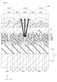
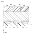
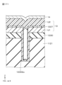
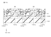
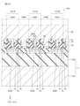
- FIG. 1 is a diagram for explaining a schematic configuration example of a display device according to a first embodiment
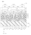
- FIG. 2 is a diagram for explaining a cross-sectional configuration example of the display device according to the first embodiment.
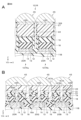
- 1A and 1B are diagrams illustrating specific examples of an organic layer.
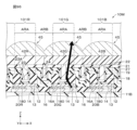
- FIG. 2 is a diagram referred to when explaining the operation of the display device according to the first embodiment.
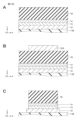
- 1A, 1B, and 1C are views referred to when explaining an example of a manufacturing method for the display device according to the first embodiment.
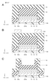
- 1A, 1B, and 1C are views referred to when explaining an example of a manufacturing method for the display device according to the first embodiment.
- 1A and 1B are diagrams referred to when explaining an example of a manufacturing method for the display device according to the first embodiment.
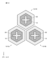
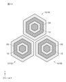
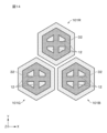
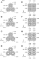
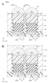
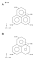
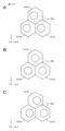
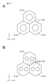
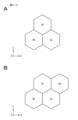
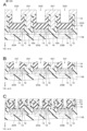
- 3A to 3C are diagrams for explaining examples of arrangement of organic layers according to the first embodiment.
- 5A to 5C are diagrams for explaining another example of the arrangement of the organic layer according to the first embodiment.
- 5A to 5C are diagrams for explaining another example of the arrangement of the organic layer according to the first embodiment.
- 5A to 5C are diagrams for explaining another example of the arrangement of the organic layer according to the first embodiment.
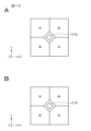
- 5A to 5C are diagrams for explaining examples of the shape of a first electrode according to the first embodiment.
- 6A to 6C are diagrams illustrating examples of other shapes of the first electrode according to the first embodiment.
- 6A to 6C are diagrams illustrating examples of other shapes of the first electrode according to the first embodiment.
- FIG. 6A to 6C are diagrams illustrating examples of other shapes of the first electrode according to the first embodiment.
- FIG. 11 is a diagram for explaining a modified example of the first embodiment.
- FIG. 11 is a diagram for explaining a modified example of the first embodiment.
- FIG. 11 is a diagram for explaining a modified example of the first embodiment.
- FIG. 11 is a diagram for explaining a modified example of the first embodiment.
- FIG. 11 is a diagram for explaining a modified example of the first embodiment.
- FIG. 11 is a diagram for explaining a modified example of the first embodiment.
- FIG. 11 is a diagram for explaining an example of a cross-sectional configuration of a display device according to a second embodiment.
- 13A and 13B are diagrams illustrating examples of shapes of recesses according to the second embodiment.
- FIG. 13 is a diagram for explaining an example of a cross-sectional configuration of a display device according to a third embodiment.
- 13A and 13B are diagrams illustrating examples of emission directions of light emitted from a light-emitting element according to a third embodiment.
- 13A to 13H are diagrams for explaining an example in which the center of a groove according to the third embodiment is not shifted from the center of a sub-pixel.
- 13A to 13H are diagrams for explaining an example in which the center of a groove according to the third embodiment is misaligned with the center of a sub-pixel.
- FIG. 13 is a diagram for explaining an example of a cross-sectional configuration of a display device according to a fourth embodiment.
- FIG. 13A and 13B are diagrams for explaining the operation of the display device according to the fourth embodiment.
- 13A to 13C are diagrams referred to when explaining an example of a manufacturing method for a display device according to a fourth embodiment.
- 13A to 13C are diagrams referred to when explaining an example of a manufacturing method for a display device according to a fourth embodiment.
- 13A and 13B are diagrams for explaining a modified example of the display device according to the fourth embodiment.
- FIG. 13 is a diagram for explaining a modified example of the fourth embodiment.
- FIG. 13 is a diagram for explaining a modified example of the fourth embodiment.
- FIG. 13 is a diagram for explaining a modified example of the fourth embodiment.
- FIG. 13 is a diagram for explaining a modified example of the fourth embodiment.
- FIG. 13 is a diagram for explaining a modified example of the fourth embodiment.
- FIG. 13 is a diagram for explaining a modified example of the fourth embodiment.
- FIG. 13 is a diagram for explaining a modified example of
- FIG. 13 is a diagram for explaining a modified example of the fourth embodiment.
- 13A and 13B are diagrams illustrating an example of the arrangement of reflective partition portions according to the fourth embodiment.
- FIG. 13 is a partial cross-sectional view for explaining a cross-sectional configuration example of a display device according to a fifth embodiment.
- FIG. 13 is a partial cross-sectional view for explaining another cross-sectional configuration example of the display device according to the fifth embodiment.
- FIG. 13 is a partial cross-sectional view for explaining another cross-sectional configuration example of the display device according to the fifth embodiment.
- FIG. 13 is a partial cross-sectional view for explaining another cross-sectional configuration example of the display device according to the fifth embodiment.
- FIG. 13 is a partial cross-sectional view for explaining another cross-sectional configuration example of the display device according to the fifth embodiment.
- FIG. 13 is a partial cross-sectional view for explaining another cross-sectional configuration example of the display device according to the fifth embodiment.
- FIG. 13 is a partial cross-sectional view for explaining another cross-sectional configuration example of the display device according to the fifth embodiment.
- FIG. 13 is a partial cross-sectional view for explaining another cross-sectional configuration example of the display device according to the fifth embodiment.
- 13A to 13C are diagrams for explaining the operation of the display device according to the fifth embodiment.
- FIG. 13 is a diagram for explaining a modified example of the fifth embodiment.
- FIG. 13 is a partial cross-sectional view for explaining a cross-sectional configuration example of a display device according to a sixth embodiment.
- FIG. 13 is a partial cross-sectional view for explaining the operation of the display device according to the sixth embodiment.
- FIG. 13A and 13B are diagrams for explaining the positional relationship between the first contact portion CT1 and the second contact portion CT2 according to the sixth embodiment.
- FIG. 23 is a partial cross-sectional view for explaining a cross-sectional configuration example of a display device according to a modified example of the sixth embodiment.
- FIG. 13 is a partial cross-sectional view for explaining the operation of the display device according to the modified example of the sixth embodiment.
- 13 is a diagram for explaining the positional relationship between the first contact portion CT1 and the second contact portion CT2 according to a modification of the sixth embodiment.
- FIG. FIG. 23 is a partial cross-sectional view for explaining a cross-sectional configuration example of a display device according to another modified example of the sixth embodiment.
- FIG. 23 is a partial cross-sectional view for explaining the operation of a display device according to another modified example of the sixth embodiment.
- FIG. 23 is a diagram for explaining the positional relationship between the first contact portion CT1 and the second contact portion CT2 according to another modified example of the sixth embodiment.
- 1A to 1E are diagrams for explaining a number of examples of arrangements of the first contact portion and the second contact portion.
- FIG. 13 is a partial cross-sectional view for explaining a cross-sectional configuration example of a display device according to a seventh embodiment.
- 13A and 13B are partial cross-sectional views for explaining the operation of the display device according to the seventh embodiment.
- 13A to 13D are diagrams to be referred to when explaining an example of a manufacturing method for a display device according to a seventh embodiment.
- 13A and 13B are views referred to when explaining an example of a manufacturing method for a display device according to a seventh embodiment.
- 13A and 13B are views referred to when explaining an example of a manufacturing method for a display device according to a seventh embodiment.
- 13A to 13C are views referred to when explaining another example of a manufacturing method for the display device according to the seventh embodiment.
- 13A to 13C are diagrams to be referred to when explaining another example of a manufacturing method for the display device according to the seventh embodiment.
- 13 is a diagram for explaining an example of a light-emitting region of a display device according to a seventh embodiment.
- FIG. FIG. 13 is a diagram for explaining the effect obtained in the seventh embodiment.
- FIG. 13 is a diagram for explaining a modified example of the seventh embodiment.
- FIG. 13 is a diagram for explaining a modified example of the seventh embodiment.
- FIG. 13 is a diagram for explaining a modified example of the seventh embodiment.
- FIG. 13 is a diagram for explaining a modified example of the seventh embodiment.
- FIG. 13 is a diagram for explaining a modified example of the seventh embodiment.
- 13A to 13F are diagrams for explaining a modification of the seventh embodiment.
- FIG. 13 is a diagram for explaining a modified example of the seventh embodiment.
- 13A to 13C are diagrams for explaining a modified example of the seventh embodiment.
- 13A and 13B are diagrams for explaining a modified example of the seventh embodiment.
- FIG. 23 is a diagram for explaining an example of the configuration of a pixel unit according to an eighth embodiment.
- 11 is a diagram for explaining another configuration example of the pixel portion.
- FIG. 23 is a diagram for explaining an example of the configuration of a pixel unit according to an eighth embodiment.
- 11 is a diagram for explaining another configuration example of the pixel portion.
- FIG. 13 is a diagram for explaining an example of a cross-sectional configuration of another pixel unit.
- FIG. FIG. 13 is a partial cross-sectional view for explaining a cross-sectional configuration example of a display device according to a ninth embodiment.
- 13A to 13C are diagrams referred to when explaining an example of a manufacturing method for a display device according to a ninth embodiment.
- 13A to 13C are diagrams referred to when explaining an example of a manufacturing method for a display device according to a ninth embodiment.
- 13A to 13C are diagrams referred to when explaining an example of a manufacturing method for a display device according to a ninth embodiment.
- 13A to 13C are diagrams referred to when explaining an example of a manufacturing method for a display device according to a ninth embodiment.
- 13A to 13C are diagrams referred to when explaining an example of a manufacturing method for a display device according to a ninth embodiment.
- 13A to 13C are diagrams referred to when explaining an example of a manufacturing method for a display device according to a ninth embodiment.
- 13A and 13B are diagrams for explaining a modified example of the ninth embodiment.
- 13A and 13B are diagrams for explaining a modified example of the ninth embodiment.
- 13A and 13B are diagrams for explaining a modified example of the ninth embodiment.
- 13A to 13C are views referred to when explaining an example of a manufacturing method for a display device according to a modified example of the ninth embodiment.
- 13A to 13C are views referred to when explaining an example of a manufacturing method for a display device according to a modified example of the ninth embodiment.
- FIG. 23 is a partial cross-sectional view for explaining a cross-sectional configuration example of a display device according to a tenth embodiment.
- 23A to 23D are diagrams for explaining an example of the function of the display device according to the tenth embodiment.
- 23A to 23D are diagrams for explaining an example of the function of the display device according to the tenth embodiment.
- 11A and 11B are diagrams for explaining examples of arrangement of insulating layers according to positions of sub-pixels.
- 13A and 13B are diagrams for explaining another example of the arrangement of the insulating layer.
- FIG. 23 is a partial cross-sectional view for explaining a cross-sectional configuration example of a display device according to an eleventh embodiment.
- 19A to 19C are diagrams for explaining an example of the operation of the display device according to the eleventh embodiment.
- FIG. 23 is a diagram for explaining a modified example of the eleventh embodiment.
- FIG. 23 is a diagram for explaining a modified example of the eleventh embodiment.
- FIG. 23 is a diagram for explaining a modified example of the eleventh embodiment.
- 23A to 23C are diagrams illustrating an example of a manufacturing method for a display device according to a modified example of the eleventh embodiment.
- 23A to 23C are diagrams illustrating an example of a manufacturing method for a display device according to a modified example of the eleventh embodiment.
- 23A and 23B are diagrams for explaining an example of a manufacturing method for a display device according to a modified example of the eleventh embodiment.
- 12A and 12B are diagrams for explaining examples of shapes of openings formed by a light reflecting layer according to an eleventh embodiment.
- 12A and 12B are diagrams for explaining examples of shapes of openings formed by a light reflecting layer according to an eleventh embodiment.
- 12A to 12C are diagrams for explaining examples of shapes of openings formed by a light reflecting layer according to an eleventh embodiment.
- 12A and 12B are diagrams for explaining examples of shapes of openings formed by a light reflecting layer according to an eleventh embodiment.
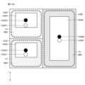
- 1A and 1B are diagrams for explaining an example of an arrangement of sub-pixels.
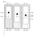
- 13A and 13B are diagrams for explaining other examples of arrangement of sub-pixels.
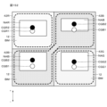
- 13A and 13B are diagrams for explaining other examples of arrangement of sub-pixels.
- 1A and 1B are diagrams for explaining examples of cathode contact arrangements.
- FIG. 23 is a partial cross-sectional view for explaining a cross-sectional configuration example of a display device according to a twelfth embodiment.
- 1A and 1B are diagrams for explaining a configuration example of a display device according to a reference example.
- 12A and 12B are diagrams for explaining a configuration example of a display device according to a twelfth embodiment.
- FIG. 23 is a diagram for explaining the effects obtained in the twelfth embodiment.
- 23A and 23B are diagrams for explaining a modified example of the twelfth embodiment.
- 23A and 23B are diagrams for explaining a modified example of the twelfth embodiment.
- 23A and 23B are diagrams for explaining a modified example of the twelfth embodiment.
- 23A to 23C are diagrams illustrating an example of a manufacturing method for a display device according to a twelfth embodiment.
- 23A to 23C are diagrams illustrating an example of a manufacturing method for a display device according to a twelfth embodiment.
- 23A to 23C are diagrams illustrating an example of a manufacturing method for a display device according to a twelfth embodiment.
- 23A and 23B are diagrams for explaining an example of a manufacturing method for a display device according to a twelfth embodiment.
- FIG. 23 is a diagram for explaining points to be considered in the thirteenth embodiment.
- FIG. 23 is a partial cross-sectional view for explaining a cross-sectional configuration example of a display device according to a thirteenth embodiment.
- 23A and 23B are diagrams illustrating a first example of a manufacturing method for a display device according to a thirteenth embodiment.
- 23A to 23C are diagrams illustrating a first example of a manufacturing method for a display device according to a thirteenth embodiment.
- 23A and 23B are diagrams for explaining a second example of a manufacturing method for the display device according to the thirteenth embodiment.
- 23A to 23C are diagrams illustrating a second example of a manufacturing method for the display device according to the thirteenth embodiment.
- 23A and 23B are diagrams for explaining a third example of a manufacturing method for the display device according to the thirteenth embodiment.
- 23A to 23C are diagrams illustrating a third example of a manufacturing method for the display device according to the thirteenth embodiment.
- 26A and 26B are diagrams for explaining an example of a manufacturing method for a display device according to a modified example of the thirteenth embodiment.
- 26A to 26C are diagrams illustrating an example of a manufacturing method for a display device according to a modified example of the thirteenth embodiment.
- FIG. 23 is a partial cross-sectional view for explaining a cross-sectional configuration example of a display device according to a modified example of the thirteenth embodiment.
- FIG. 23 is a partial cross-sectional view for explaining a cross-sectional configuration example of a display device according to a fourteenth embodiment. This figure is referred to when explaining points to be considered in the fourteenth embodiment. This figure is referred to when explaining points to be considered in the fourteenth embodiment.
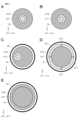
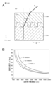
- 1A and 1B are diagrams illustrating an example of characteristics of a diffraction grating.
- 23A to 23C are diagrams for explaining a first angle, a second angle, and a third angle according to the fourteenth embodiment; FIG.
- FIG. 23 is a diagram for explaining an example of the interrelationship between the first angle, the second angle, and the third angle according to the fourteenth embodiment.
- FIG. 23 is a diagram for explaining another example of the interrelationship between the first angle, the second angle, and the third angle according to the fourteenth embodiment.
- FIG. 23 is a diagram for explaining another example of the interrelationship between the first angle, the second angle, and the third angle according to the fourteenth embodiment.
- FIG. 23 is a diagram for explaining another example of the interrelationship between the first angle, the second angle, and the third angle according to the fourteenth embodiment.
- FIG. 23 is a diagram for explaining a modified example of the fourteenth embodiment.
- FIG. 23 is a diagram for explaining a modified example of the fourteenth embodiment.
- FIG. 23 is a diagram for explaining a modified example of the fourteenth embodiment.
- FIG. 23 is a diagram for explaining a modified example of the fourteenth embodiment.
- FIG. 23 is a diagram for explaining a modified example of the fourteenth embodiment.
- FIG. 23 is a diagram for explaining a modified example of the fourteenth embodiment.
- 1A is a schematic cross-sectional view for explaining a first example of a resonator structure
- FIG. 1B is a schematic cross-sectional view for explaining a second example of a resonator structure
- 1A is a schematic cross-sectional view for explaining a third example of a resonator structure
- FIG. 1B is a schematic cross-sectional view for explaining a fourth example of a resonator structure.
- FIG. 13A is a schematic cross-sectional view for explaining a fifth example of a resonator structure
- FIG. 13B is a schematic cross-sectional view for explaining a sixth example of a resonator structure.
- FIG. 13 is a schematic cross-sectional view for explaining a seventh example of a resonator structure.
- 1A, 1B, and 1C are conceptual diagrams for explaining the relationship between a normal line LN passing through the center of the light-emitting portion, a normal line LN' passing through the center of the lens member, and a normal line LN" passing through the center of the wavelength selection portion, respectively.
- FIG. 1 is a conceptual diagram for explaining the relationship between a normal line LN passing through the center of a light-emitting portion, a normal line LN' passing through the center of a lens member, and a normal line LN" passing through the center of a wavelength selection portion.
- FIG. 1A and 1B are conceptual diagrams for explaining the relationship between a normal line LN passing through the center of the light-emitting portion, a normal line LN' passing through the center of the lens member, and a normal line LN" passing through the center of the wavelength selection portion, respectively.
- FIG. 1 is a conceptual diagram for explaining the relationship between a normal line LN passing through the center of a light-emitting portion, a normal line LN' passing through the center of a lens member, and a normal line LN" passing through the center of a wavelength selection portion.
- FIG. FIG. 1 is a diagram to be referred to when explaining an example of an inter-pixel structure for preventing inter-pixel leakage.
- FIG. 1 is a diagram to be referred to when explaining an example of an inter-pixel structure for preventing inter-pixel leakage.
- FIG. 1 is a diagram to be referred to when explaining an example of an inter-pixel structure for preventing inter-pixel leakage.
- FIG. 1 is a diagram to be referred to when explaining an example of an inter-pixel structure for preventing inter-pixel leakage.
- FIG. 1 is a diagram to be referred to when explaining an example of an inter-pixel structure for preventing inter-pixel leakage.
- FIG. 1 is a diagram to be referred to when explaining an example of an inter-pixel structure for preventing inter-pixel leakage.
- FIG. 1 is a diagram to be referred to when explaining an example of an inter-pixel structure for preventing inter-pixel leakage.
- FIG. 1 is a diagram to be referred to when explaining an example of an inter-pixel structure for preventing inter-pixel leakage.
- FIG. 1 is a diagram to be referred to when explaining an example of an inter-pixel structure for preventing inter-pixel leakage.
- FIG. 1 is a diagram to be referred to when explaining an example of an inter-pixel structure for preventing inter-pixel leakage.
- FIG. 1 is a diagram to be referred to when explaining an example of an inter-pixel structure for preventing inter-pixel leakage.
- FIG. 1 is a diagram to be referred to when explaining an example of an inter-pixel structure for
- FIG. 1 is a diagram to be referred to when explaining an example of an inter-pixel structure for preventing inter-pixel leakage.
- FIG. 1 is a diagram to be referred to when explaining an example of an inter-pixel structure for preventing inter-pixel leakage.
- 1A is a front view showing an example of the external appearance of a digital still camera
- FIG. 1 is a perspective view showing an example of the appearance of a head mounted display.
- FIG. 1 is a perspective view showing an example of the appearance of a television device.
- 1 is a perspective view showing an example of the appearance of a see-through head mounted display.
- FIG. 1 is a perspective view showing an example of the appearance of a smartphone.
- FIG. 1A is a diagram showing an example of the interior of a vehicle from the rear to the front of the vehicle
- FIG. 1B is a diagram showing an example of the interior of a vehicle from the diagonally rear to the diagonally front of the vehicle.
- FIG. 13 is a diagram for explaining a modified example.
- An example of the display device according to the embodiment of the present disclosure is an organic EL display device.
- the display device according to the first embodiment has a plurality of luminescent colors.
- the display device 10A has a plurality of pixels, and each pixel is formed by a combination of a plurality of sub-pixels (sub-pixels 101) corresponding to a plurality of color types (luminescent colors).
- the display device 10A has a plurality of sub-pixels 101 arranged two-dimensionally.
- the display device 10A may be a micro display.
- the display device 10A may be provided in a VR device, a mixed reality (MR) device, an AR device, an electronic view finder (EVF), a small projector, or the like.
- MR mixed reality
- EMF electronic view finder
- the display device 10A has a drive substrate 11.
- the drive substrate 11 has an effective pixel area AR1 and a peripheral area AR2 surrounding the effective pixel area AR1.
- the effective pixel area AR1 is an area that is defined as an area for emitting light generated by a plurality of light-emitting elements.
- a plurality of pixels are provided in the effective pixel area AR1.
- a plurality of sub-pixels 101 are two-dimensionally arranged in a prescribed arrangement pattern, such as a matrix, within the effective pixel area AR1.
- Subpixel 101 includes subpixels 101R, 101G, and 101B.
- Subpixel 101R displays red
- subpixel 101G displays green
- subpixel 101B displays blue.
- subpixel 101 when subpixels 101R, 101G, and 101B are referred to collectively without distinction, they are referred to as subpixel 101.
- R, G, and B are added to the reference numerals for the components of subpixels 101R, 101G, and 101B as appropriate.
- the combination of adjacent subpixels 101R, 101G, and 101B constitutes one pixel.
- a control circuit 2 an H driver 3A, and a V driver 3B are provided in the peripheral area AR2 of the display device 10A.
- the control circuit 2 controls the driving of the H driver 3A and the V driver 3B.
- the H driver 3A and the V driver 3B control the driving of the sub-pixels 101 by a known method.
- the top emission method refers to a method in which the light emitting element is disposed closer to the effective pixel area AR1 side than the drive substrate 11. Therefore, in the display device 10A, the light generated from the light emitting element is directed in the +Z direction and emitted to the outside.
- the surface that is the display surface side in the effective pixel area AR1 of the display device 10A (the area hatched in FIG. 1) is referred to as the first surface (upper surface), and the surface that is the back surface side of the display device 10 is referred to as the second surface (lower surface).
- the display device according to the present disclosure may use a bottom emission method. In the bottom emission method, the light generated from the light emitting element is directed in the -Z direction and emitted to the outside.
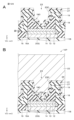
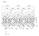
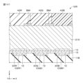
- FIG. 2 is an enlarged view showing a cross-sectional configuration example of a region XS surrounded by a dashed line in Fig. 1 .
- sub-pixels 101R, 101B, and 101G are arranged in a predetermined array along the X direction on the drive substrate 11.
- the sub-pixels 101R, 101B, and 101G are described as having the same configuration, but there may be differences in configuration between the sub-pixels 101.
- the display device 10A includes a plurality of light-emitting elements 20.
- the plurality of light-emitting elements 20 are composed of a first electrode 12, an organic layer 13 including a light-emitting layer, and a second electrode 14.
- the light-emitting elements 20 are, for example, white light-emitting elements such as white OLEDs or white Micro-OLEDs (MOLEDs).
- the colorization method used in the display device 10A is a method that uses white light-emitting elements and color filters, which will be described later.
- the display device 10A has a drive substrate 11.
- the drive substrate 11 is a so-called backplane, and drives a plurality of light-emitting elements 20.
- the drive substrate 11 has, for example, a base material 11A and an interlayer insulating layer 11B laminated on the base material 11A.
- the interlayer insulating layer 11B may be formed by being laminated on the base material 11A, or a part of it may be formed directly on the base material 11A by a semiconductor process.
- the substrate 11A may be a semiconductor substrate such as a silicon substrate, or an insulating substrate such as a glass substrate, quartz, or resin substrate with low moisture and oxygen permeability.
- Semiconductor substrates include, for example, amorphous silicon, polycrystalline silicon, or single crystal silicon.
- glass substrates include, for example, high strain point glass, soda glass, borosilicate glass, forsterite, lead glass, or quartz glass.
- resin substrates include, for example, at least one selected from the group consisting of polymethyl methacrylate, polyvinyl alcohol, polyvinyl phenol, polyether sulfone, polyimide, polycarbonate, polyethylene terephthalate, and polyethylene naphthalate.
- the substrate 11A has, for example, a thin plate shape.
- the substrate 11A may be flexible.
- the interlayer insulating layer 11B is made of, for example, an organic material or an inorganic material.
- the organic material includes, for example, at least one of polyimide and acrylic resin.
- the inorganic material includes, for example, at least one of silicon oxide, silicon nitride, silicon oxynitride, and aluminum oxide.
- Various circuits that drive the multiple light-emitting elements 20 are provided within the interlayer insulating layer 11B.
- Examples of the various circuits include a drive circuit that controls the driving of the light-emitting elements 20 and a power supply circuit that supplies power to the multiple light-emitting elements 20 (neither of which are shown).
- the various circuits are restricted from exposure to the outside by the interlayer insulating layer 11B.
- These drive circuits (not shown) are connected to appropriate locations such as the first electrode 12.
- a plurality of light-emitting elements 20 are provided on the first surface of the interlayer insulating layer 11B.
- the light-emitting elements 20 are, for example, organic electroluminescence elements (organic EL elements).
- the plurality of light-emitting elements 20 each emit light of a color corresponding to the color type of the sub-pixel 101 from the light-emitting surface.
- light-emitting elements 20R, 20G, and 20B are formed in the sub-pixels 101R, 101G, and 101B, respectively.
- the plurality of light-emitting elements 20 are laid out in a manner corresponding to the arrangement of the sub-pixels 101 of the respective color types. In this specification, when the types of the light-emitting elements 20R, 20G, and 20B are not particularly distinguished from one another, the term "light-emitting element 20" is used.
- the light-emitting element 20 has a laminated structure in which a first electrode 12, an organic layer 13, and a second electrode 14 are laminated in this order from the drive substrate 11 side in the direction from the second surface to the first surface (+Z direction).
- a plurality of first electrodes 12 are provided on the first surface side of the driving substrate 11.
- the first electrodes 12 are, for example, anode electrodes.
- the first electrodes 12 may be transparent electrodes having optical transparency.
- the first electrode 12 is composed of at least one of a metal layer and a metal oxide layer.
- the first electrode 12 may be composed of a single layer of a metal layer or a metal oxide layer, or a laminated layer of a metal layer and a metal oxide layer.
- the metal layer contains at least one metal element selected from the group consisting of, for example, chromium (Cr), gold (Au), platinum (Pt), nickel (Ni), copper (Cu), molybdenum (Mo), titanium (Ti), tantalum (Ta), aluminum (Al), magnesium (Mg), iron (Fe), tungsten (W) and silver (Ag).
- the metal layer may contain at least one metal element as a constituent element of an alloy.
- alloys include aluminum alloys and silver alloys.
- Specific examples of aluminum alloys include, for example, AlNd and AlCu.
- the metal oxide layer includes, for example, at least one of a mixture of indium oxide and tin oxide (ITO), a mixture of indium oxide and zinc oxide (IZO), and titanium oxide (TiO).
- ITO indium oxide and tin oxide
- IZO indium oxide and zinc oxide
- TiO titanium oxide
- the first electrodes 12 are electrically separated for each subpixel 101. That is, a plurality of first electrodes 12 are provided on the first surface side of the drive substrate 11, and each first electrode 12 is provided for each subpixel 101.
- the organic layer 13 is an organic light-emitting layer provided between the first electrode 12 and the second electrode 14.
- the organic layer 13 is provided separately for each sub-pixel 101.
- the organic layer 13 may be configured to be provided in common to the sub-pixels 101.
- the organic layer 13 is configured to be capable of emitting white light. However, this does not prohibit the emission color of the organic layer 13 from being other than white, and colors such as red, blue, and green may be adopted. In other words, the emission color of the organic layer 13 may be, for example, any one of white, red, blue, and green.
- the organic layer 13 has a structure in which, for example, a hole injection layer, a hole transport layer, a light-emitting layer, and an electron transport layer are stacked in this order from the first electrode 12 toward the second electrode 14.
- An electron injection layer may be provided between the electron transport layer and the second electrode 14.
- the electron injection layer is intended to increase the efficiency of electron injection. Note that the structure of the organic layer 13 is not limited to this, and layers other than the light-emitting layer are provided as necessary.
- the hole injection layer is intended to increase the efficiency of hole injection into the light-emitting layer, and is also a buffer layer to suppress leakage.
- the hole transport layer is intended to increase the efficiency of hole transport to the light-emitting layer.
- the electron transport layer is intended to increase the efficiency of electron transport to the light-emitting layer.
- the light-emitting layer generates light when an electric field is applied, causing electrons and holes to recombine.
- the light-emitting layer is an organic compound layer that contains an organic light-emitting material.
- the organic layer 13 may be composed of a laminate including an organic light-emitting layer, and in that case, some layers of the laminate (e.g., an electron injection layer) may be an inorganic layer.
- the organic layer 13 may be an OLED layer having a single light-emitting unit U as shown in Figure 3A, an OLED layer having two light-emitting units U1 and U2 (tandem structure) as shown in Figure 3B, or an OLED layer having a structure other than these.
- the organic layer 13 having a single light-emitting unit U has a structure in which, for example, a hole injection layer 131, a hole transport layer 132, a red light-emitting layer 130R, a light-emitting separation layer 133, a blue light-emitting layer 130B, a green light-emitting layer 130G, an electron transport layer 134, and an electron injection layer 135 are laminated in this order from the first electrode 12 to the second electrode 14.
- the OLED layer having two light-emitting units U1 and U2 has a structure in which, for example, from the first electrode 12 toward the second electrode 14, a hole injection layer 131, a hole transport layer 132, a blue light-emitting layer 130B, an electron transport layer 136, a charge generation layer 137, a hole transport layer 138, a yellow light-emitting layer 130Y, an electron transport layer 134, and an electron injection layer 135 are laminated in this order.
- a second electrode 14 is provided on the upper side of the organic layer 13.
- the second electrode 14 is, for example, a cathode.
- the second electrode 14 is connected to a cathode contact (not shown) by a predetermined wiring structure.
- a portion of the second electrode 14 corresponding to the sub-pixel 101 (a portion corresponding to the light-emitting element 20) is provided so as to face the first electrode 12.
- the second electrode 14 is provided separately for each of the plurality of sub-pixels 101.
- the second electrode 14 may be provided as a common electrode for the plurality of sub-pixels 101.
- the second electrode 14 is preferably a transparent electrode that is transparent to the light generated in the organic layer 13.
- the transparent electrode referred to here includes an electrode formed of a transparent conductive layer and an electrode formed of a laminated structure having a transparent conductive layer and a semi-transmissive reflective layer.
- the transparent conductive layer is preferably made of a transparent conductive material with good light transmission and a small work function.
- the transparent conductive layer can be made of, for example, a metal oxide.
- examples of the material for the transparent conductive layer include a material containing at least one of a mixture of indium oxide and tin oxide (ITO), a mixture of indium oxide and zinc oxide (IZO), and zinc oxide (ZnO).
- the semi-transmissive reflective layer can be formed, for example, from a metal layer.
- the material of the semi-transmissive reflective layer can be, for example, one containing at least one metal element selected from the group consisting of magnesium (Mg), aluminum (Al), silver (Ag), gold (Au) and copper (Cu).
- the metal layer may contain at least one of the above metal elements as a constituent element of an alloy. Specific examples of the alloy include an MgAg alloy and an AgPdCu alloy.
- the first electrode 12 may be a cathode and the second electrode 14 may be an anode.
- an insulating layer is formed between adjacent first electrodes 12.
- an interpixel insulating layer 16 is formed between adjacent first electrodes 12.
- the interpixel insulating layer 16 may be an organic insulating layer, an inorganic insulating layer, or a laminate of these.
- the organic insulating layer includes at least one selected from the group consisting of, for example, polyimide resin, acrylic resin, novolac resin, and the like.
- the inorganic insulating layer includes at least one selected from the group consisting of, for example, silicon oxide (SiOx), silicon nitride (SiNx), silicon oxynitride (SiOxNy), and the like.
- the interpixel insulating layer 16 has an opening 16A, and the first electrode 12 is exposed through this opening 16A.
- a first protective layer 18 is formed so as to partially cover a first surface side (a first surface side of the second electrode 14) of the light-emitting element 20.
- the first protective layer 18 makes the first surface of the light-emitting element 20 less likely to be exposed to the outside air, and suppresses the intrusion of moisture from the external environment into the light-emitting element 20.
- the first protective layer 18 is formed of an insulating material.
- a thermosetting resin can be used as the insulating material.
- Other insulating materials may be SiO, SiON, AlO, TiO, SiN, etc.
- examples of the first protective layer 18 include a CVD film containing SiO, SiON, etc., and an ALD film containing AlO, TiO, SiO, etc.
- the CVD film refers to a film formed using chemical vapor deposition.
- the ALD film refers to a film formed using atomic layer deposition.
- the first protective layer 18 may be formed as a single layer, or may have a structure in which multiple layers are stacked.
- an isolation protective layer 19 is formed as an inter-element isolation wall so as to cover the side end faces of the light-emitting elements 20, the side end faces of the first protective layer 18, and the upper end face of the first protective layer 18.
- the isolation protective layer 19 is disposed between adjacent light-emitting elements 20, and separates the first electrode 12, the organic layer 13, and the second electrode 14 for each sub-pixel 101.
- the isolation protective layer 19 is made of an insulator.
- Examples of the isolation protective layer 19 include an inorganic insulating film and an organic insulating film.
- Examples of the inorganic insulating film include SiO 2 , SiN, and SiON.
- Examples of the organic insulating film include polyimide.
- a second protective layer 21 is formed over the entire first surface side of the separation protective layer 19.
- the second protective layer 21 may be omitted.
- the same material as that of the first protective layer 18 may be used as the material of the second protective layer 21.
- a refractive layer 22 is formed on the first surface of the second protective layer 21.
- the material of the refractive layer 22 may be an insulating material or a resin material similar to that of the first protective layer 18.
- the refractive layer 22 may be an air layer.
- the refractive index of the refractive layer 22 is smaller than the refractive index of the protective layer in contact with the refractive layer 22 (in this embodiment, the second protective layer 21).
- a color filter section and a lens may be further disposed on the first surface of the refractive layer 22.
- the refractive layer 22 functions, for example, as a planarizing layer for obtaining flatness of the surface for forming the color filter section.
- a planarizing layer may be provided separately from the refractive layer 22.
- the refractive layer 22 also functions as a protective layer for preventing foreign matter such as moisture from entering the light-emitting element 20, etc.
- the display device 10A may be configured without some of the above-mentioned components.
- the display device 10A may be configured to have known components other than the above-mentioned components.
- an intra-pixel area ARA which is an area within the sub-pixel 101
- an inter-pixel area ARB which is an area between the sub-pixels 101
- the intra-pixel area ARA is, for example, an area including the light-emitting element 20, and is set as an area inside the outer edge of the first protective layer 18, for example.
- the area inside the outer edge of the separation protective layer 19 may be set as the intra-pixel area ARA.
- the inter-pixel area ARB is an area other than the intra-pixel area ARA, and is set as an area between the outer edges of the first protective layer 18 in the sub-pixels 101, for example.
- a groove portion 23 is formed in the intra-pixel area ARA.
- the groove portion 23 is formed near the center of the intra-pixel area ARA.
- the groove portion 23 is obtained by partially removing the first protective layer 18 and the isolation protective layer 19 in the intra-pixel area ARA and disposing the second protective layer 21 in that location.
- the second protective layer 21, the second electrode 14, the organic layer 13, and the first electrode 12 are interposed between the end face 23A of the groove portion 23 (the lower surface of the groove portion 23) and the first surface of the drive substrate 11.
- a groove portion 24 is also formed in the inter-pixel region ARB.
- the groove portion 24 is a step formed in the inter-pixel region ARB.
- the refractive layer 22 is disposed (filled) in the grooves 23 and 24.
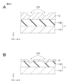
- the operation of the display device 10A according to this embodiment will be described with reference to FIG. 4.
- the light L1 directed toward the center of the pixel area ARA is refracted in the front direction (upward) due to the difference in the refractive index between the second protective layer 21 and the refractive layer 22 in the pixel area ARA.
- the light L2 directed toward the center of the inter-pixel area ARB is refracted in the front direction (upward) due to the difference in the refractive index between the second protective layer 21 and the refractive layer 22 in the inter-pixel area ARB.
- the light (light L1, L2) emitted from the end of the sub-pixel 101 (for example, the sub-pixel 101G) and directed in the horizontal direction (diagonal horizontal direction) can be directed in the front direction, thereby improving the light extraction efficiency.
- the refractive index of the refractive layer 22 is described as being smaller than the refractive index of the second protective layer 21, but the refractive index of the refractive layer 22 may be larger than the refractive index of the second protective layer 21 as long as the above-mentioned effect can be achieved.
- the interlayer insulating layer 11B is formed.
- a metal layer and a metal oxide layer are sequentially formed on the first surface of the drive substrate 11 by, for example, a sputtering method, and then the metal layer and the metal oxide layer are patterned by, for example, a photolithography technique and an etching technique.
- an interpixel insulating layer 16 is formed on the first surface of the drive substrate 11 so as to cover the multiple first electrodes 12 by, for example, a CVD (Chemical Vapor Deposition) method.
- openings 16A are formed in the interpixel insulating layer 16 in the portions located on the first surfaces of the first electrodes 12 by, for example, a photolithography technique and a dry etching technique.
- an organic layer 13 is formed on the first surface of the first electrode 12 and on the first surface of the interpixel insulating layer 16, for example, by vapor deposition.
- a second electrode 14 is formed over the entire first surface side of the drive substrate 11, for example, by vapor deposition or sputtering.
- a first protective layer 18 is formed over the entire first surface side of the drive substrate 11, for example, by CVD or vapor deposition.
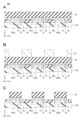
- a resist 31 is placed on the first surface of the first protective layer 18. Then, an etching process is performed to remove unnecessary parts of the first protective layer 18, the second electrode 14, and the organic layer 13, as shown in FIG. 5C.
- the isolation protective layer 19 is formed over the entire surface by vapor deposition or sputtering. Then, as shown in FIG. 6B, after resist 31 is placed, unnecessary portions of the isolation protective layer 19 and the first protective layer 18 are removed, forming a groove 38A in the intra-pixel area ARA as shown in FIG. 6C. Furthermore, as the resist 31 is removed, a groove portion 38B is formed in the inter-pixel area ARB.
- a second protective layer 21 is formed over the entire surface by, for example, vapor deposition or sputtering, to form grooves 23 in the intra-pixel area ARA and grooves 24 in the inter-pixel area ARB.
- a refractive layer 22 is formed on the first surface of the second protective layer 21. Note that, although not explained or illustrated, subsequent steps include providing a color filter, an opposing substrate opposing the drive substrate 11, and the like.
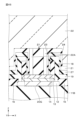
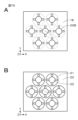
- Fig. 8 to Fig. 11 are plan views of the drive substrate 11 from the +Z direction. Note that in Fig. 8 to Fig. 11, the location indicated by reference numeral 32 is a laminate (laminate 32) including the organic layer 13, the second electrode 14, and the first protective layer 18.
- the laminate 32 including the organic layer 13 may be formed independently between each subpixel 101. Also, as shown in FIG. 9, the laminate 32 including the organic layer 13 may be formed independently between each subpixel 101. In the example shown in FIG. 9, the first electrode 12 is shared between subpixels of the same color (subpixel 101B in the illustrated example). This is not limited to this example, and as shown in FIGS. 10 and 11, the laminate 32 including the organic layer 13 may be shared between subpixels 101.
- Figs. 12 to 15 are plan views of the driving substrate 11 from the +Z direction.
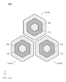
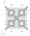
- the shape of the first electrode 12 in the sub-pixel 101 may be asymmetric (for example, a cross shape).
- the first electrode 12 may be isolated in the sub-pixel 101.
- the first electrode 12 may be composed of a plurality of electrodes formed at a distance from each other.
- the shape or size of the first electrode 12 may be different in the driving substrate 11 or for each sub-pixel 101.
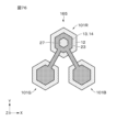
- FIG. 16 is a diagram showing a cross-sectional configuration example of a display device (display device 10B) according to a first modified example.
- the display device 10B has an auxiliary electrode 27.
- the auxiliary electrode 27 is formed, for example, between the separation protective layer 19 and the second protective layer 21, and is connected to the second electrode 14 of each subpixel 101.
- the second protective layer 21 is formed for the auxiliary electrode 27, and also functions as an auxiliary electrode protective layer that protects the auxiliary electrode 27.
- the auxiliary electrode 27 electrically connects adjacent second electrodes 14 to each other.
- the auxiliary electrode 27 connected to each second electrode 14 is connected to a cathode contact (not shown) in the peripheral region AR2.
- the second protective layer 21, the auxiliary electrode 27, the second electrode 14, the organic layer 13, and the first electrode 12 are interposed between the end surface 23A of the groove portion 23 and the drive substrate 11.
- the auxiliary electrode 27 is a transparent electrode that is transparent to light generated in the organic layer 13.
- the transparent electrode also includes a semi-transparent reflective layer.
- FIG. 17 is a diagram showing a cross-sectional configuration example of a display device (display device 10C) according to a second modified example.
- the second electrode 14 and the organic layer 13 located below the end face 23A of the groove portion 23 are removed.
- the second protective layer 21 and the first electrode 12 are interposed.
- the groove portion 23 is provided, the extraction efficiency of the light emitted below the end face 23A is poor, and in some cases, the area may become black dot-like or color mixing may occur. Therefore, in this modified example, the second electrode 14 and the organic layer 13 at the area below the end face 23A of the groove portion 23 are removed.
- the first electrode 12 is interposed between the end face 23A of the groove portion 23 and the drive substrate 11, and the second electrode 14 and the organic layer 13 are not interposed.
- the area below the end face 23A of the groove portion 23 can be made a non-light-emitting area, and the above-mentioned inconvenience can be avoided.
- the first electrode 12 located below the end surface 23A of the groove 23 may also be removed. With this configuration, the area below the end surface 23A of the groove 23 can be made a non-light-emitting area, and the above-mentioned inconvenience can be avoided.
- (Third Modification) 19 is a diagram showing an example of a cross-sectional configuration of a display device (display device 10D) according to a third modified example.
- a cathode contact 28 is formed on the interlayer insulating layer 11B located below the end face 23A of the groove portion 23.
- the above-mentioned auxiliary electrode 27 may be connected to the cathode contact 28 formed on the interlayer insulating layer 11B. This eliminates the need to provide a cathode contact in the peripheral region AR2, allowing the entire display device to be miniaturized.
- An insulating layer may be provided between the auxiliary electrode 27 and the first electrode 12.
- FIG. 20 is a diagram showing a cross-sectional configuration example of a display device (display device 10E) according to a fourth modified example.
- the basic configuration of the display device 10E is the same as that of the display device 10B described above. The difference is that the first electrode 12 located below the end face 23A of the groove portion 23 is removed, and an insulating layer 29 is formed in the removed area. In other words, the first electrode 12 is not interposed between the end face 23A of the groove portion 23 and the driving substrate 11, but the second electrode 14, the organic layer 13, and the insulating layer 29 are interposed.
- This modified example also allows the area below the end face 23A to be a non-light-emitting area.
- (Fifth Modification) 21 is a diagram showing an example of a cross-sectional configuration of a display device (display device 10F) according to a fifth modified example.
- the display device 10F has all of the configurations of the display devices 10B, 10C, 10D, and 10E according to the modified examples. This makes it possible to achieve the effects described in each modified example.
- the display device may have a sidewall protective film (also referred to as a sidewall, etc.) interposed between the side end surface of the organic layer 13, the second electrode 14, and the lower side surface of the first protective layer 18, and the separation protective layer 19. It is preferable that the sidewall protective film contacts the side end surface of the organic layer 13 and covers the entire side end area of the organic layer 13.
- a sidewall protective film also referred to as a sidewall, etc.
- the sidewall protective film is an insulating film, and is a processing by-product film that contains by-products (deposits) generated by the etching process.
- the sidewall protective film assists in the formation of the isolation protective layer 19 while preventing the organic layer 13 from being exposed to the external environment. Note that, although either dry etching or wet etching can be used as the etching process, from the viewpoint of more reliably realizing the deposits, it is preferable that the etching process be a dry etching process.
- a groove 23 is provided in the intra-pixel area ARA, and a refractive layer 22 is disposed in the groove 23, thereby enabling the light emitted by the light-emitting element 20 (particularly the light emitted near the outer periphery of the light-emitting element 20) to be effectively extracted to the outside.
- the emission intensity in the intra-pixel area ARA is made non-uniform.
- the display device is configured so that a first emission intensity in a first region between the end face 23A of the groove 23 in the intra-pixel area ARA and the drive substrate 11 is smaller than a second emission intensity in a second region other than the first region in the intra-pixel area ARA.
- FIG. 22 is a partial cross-sectional view (an enlarged cross-sectional view of the peripheral area of the light-emitting element 20G) for explaining an example of the cross-sectional configuration of a display device (display device 10G) according to the second embodiment.
- a first area ARC is set between the end face 23A of the groove portion 23 and the drive substrate 11, and a second area ARD other than the first area ARC in the intra-pixel area ARA is set.
- a recess is formed at a predetermined location of the first electrode 12 located in the second region ARD.
- a V-shaped recess 12A in cross section is formed on the first surface of the first electrode 12.
- An organic layer 13, a second electrode 14, and a first protective layer 18 are laminated on the first surface side of the recess 12A.
- the concave portion 12A has an inclined surface, so that the organic layer 13 is applied thinner to the concave portion 12A than to a flat portion.
- the thickness of the organic layer 13 formed on the concave portion 12A is smaller than the thickness of the organic layer 13 formed on the flat portion.
- the thickness of the organic layer 13 formed on the concave portion 12A is 60% to 70% of the thickness of the organic layer 13 formed on the flat portion.
- the shape of the recess 12A is not limited to a V-shape.
- the shape of the recess 12A may be semicircular (cone-shaped overall) in cross section.
- the recess 12A may be formed by processing the first electrode 12, or may be formed by processing a layer in contact with the second surface of the first electrode 12.
- a V-shaped recess may be formed in the interlayer insulating layer 11B, and the first electrode 12 may be formed on the first surface of the interlayer insulating layer 11B including the recess, thereby forming the recess 12A. Note that in FIGS. 23A and 23B, illustration of a contact connected to the first electrode 12 is omitted.
- the display device 10G can be manufactured, for example, as follows. Here, the differences from the example manufacturing method of the display device 10A described in the first embodiment will be mainly described. After the first electrode 12 is formed on the interlayer insulating layer 11B, a resist is placed at an appropriate location on the first surface of the first electrode 12. Then, for example, the first electrode 12 is partially removed by wet etching to form a recess 12A, and the resist is then removed. The manufacturing method described in the first embodiment can be applied to the subsequent steps.
- a recess is formed on the first surface of the interlayer insulating layer 11B by applying a photolithography technique. Then, the first electrode 12 is formed on the first surface of the interlayer insulating layer 11B to form the recess 12A.
- the display device 10G may be configured to have an auxiliary electrode 27.
- the principal ray of light emitted by the light emitting element 20 is tilted in an arbitrary direction.
- a method of tilting the principal ray in an arbitrary direction can be to shift a color filter or an on-chip lens disposed above the light source. In this method, a part of the light that reaches the color filter from the light source is blocked, causing light attenuation.
- the above-mentioned Patent Document 1 does not describe a method of controlling the light ray in an arbitrary direction.
- FIG. 24 is a diagram showing an example of the cross-sectional configuration of a display device (display device 10H) according to the third embodiment.
- Grooves 23R, 23G, and 23B are formed in the intra-pixel areas ARA of sub-pixels 101R, 101G, and 101B, respectively.
- the center CE2 of the groove portion 23R in the sub-pixel 101R is offset to the left with respect to the center CE1 of the intra-pixel area ARA, and the groove portion 23R is generally inclined to the upper left with respect to the light emission direction.
- the center CE2 of the groove portion 23G in the sub-pixel 101G is approximately coincident with the center CE1 of the intra-pixel area ARA.
- the center CE2 of the groove portion 23B in the sub-pixel 101B is offset to the right with respect to the center CE1 of the intra-pixel area ARA, and the groove portion 23B is generally inclined to the upper right with respect to the light emission direction.
- the center CE2 of the groove portion 23 means the center of the shape of the groove portion 23 when viewed in a plane, or the center of the shape formed by the outer edge of the groove portion 23.
- a waveguide is formed along the inclination of the groove 23R and the groove 23B. That is, the light emitted by the light-emitting element 20R is emitted in the upper left direction along the waveguide corresponding to the inclination of the groove 23R, as shown in FIG. 25. Also, the light emitted by the light-emitting element 20G is emitted in the front direction along the waveguide corresponding to the inclination of the groove 23G, as shown in FIG. 25. Also, the light emitted by the light-emitting element 20B is emitted in the upper right direction along the waveguide corresponding to the inclination of the groove 23B, as shown in FIG. 25. Of course, the light emission direction shown in FIG. 25 is one example.
- the groove 23G may have an inclination, and the light emitted by the light-emitting element 20G may be emitted in any direction along the waveguide corresponding to the inclination of the groove 23G.
- the inclination of the groove 23 allows the main ray of the light emitted by the light-emitting element 20 to be tilted in any direction.
- the display device 10H can be manufactured, for example, by the following method.
- the following mainly describes the differences from the example of the manufacturing method of the display device described in the first embodiment.
- the center CE2 of the end face of the groove 38A (the tip in the -Z direction, which faces the second electrode 14) is shifted from the center CE1.
- the throw of the second protective layer 21 becomes asymmetric, and as a result, the inclination of the groove portion 23 becomes asymmetric between the left and right.
- the groove portion 23 as a whole is inclined in a predetermined direction.
- the inclination direction and inclination angle of the groove portion 23 can be formed to obtain the desired emission direction of light.
- Fig. 26 and Fig. 27 are plan views of the drive substrate 11 from the +Z direction.
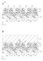
- Fig. 26A to Fig. 26H show examples in which the center CE2 of the groove portion 23 is not misaligned with the center CE1 of the sub-pixel 101 in the intra-pixel area ARA.
- Fig. 26A to Fig. 26D show examples in which the sub-pixels 101 are arranged in a delta arrangement
- Fig. 26E to Fig. 26H show examples in which the sub-pixels 101 are arranged in a square arrangement.
- FIGS. 27A to 27H show an example in which the center CE2 of the groove 23 is offset from the center CE1 of the subpixel 101 in the pixel area ARA.
- FIGS. 27A to 27H corresponds to each of FIGS. 26A to 26H.
- FIGS. 27A to 27H shows an example in which the center CE2 of the groove 23 in each of FIGS. 26A to 26H is offset to the lower right as one faces the drawing.
- FIGS. 27A to 27D show an example in which the subpixels 101 are arranged in a delta arrangement
- FIGS. 27E to 27H show an example in which the subpixels 101 are arranged in a square arrangement. Note that the direction of offset of the center CE2 shown in FIGS. 27A to 27H is just an example, and the center CE2 may be offset to the upper left or the like, for example.
- the display device 10G may have an auxiliary electrode 27.
- a space (gap) rather than a refractive layer 22 may be formed in the groove 24 in the inter-pixel region ARB.
- the organic layer 13 may be a common configuration for the sub-pixels 101.
- a groove portion 23 is provided in the intra-pixel area ARA, and a refractive layer 22 is disposed in the groove portion 23, so that light emitted by the light-emitting element 20 (particularly light emitted near the outer periphery of the light-emitting element 20) can be effectively extracted to the outside.
- a color filter is disposed in the emission direction of the refracted light, the light passing between the color filters of different colors is attenuated. In other words, the light extraction efficiency in the display device is reduced.
- This embodiment is an embodiment that addresses such a problem.
- [Example of the configuration of a display device] 28 shows an example of a cross-sectional configuration of a display device (display device 10I) according to a fourth embodiment.
- the display device 10I has a color filter unit 41.
- the color filter unit 41 is formed on, for example, a first surface of the refractive layer 22.
- a planarization layer or the like may be interposed between the color filter unit 41 and the refractive layer 22.
- An example of the color filter unit 41 is an on-chip color filter (OCCF).
- the color filter section 41 has a plurality of color filters 42 that are provided according to the color type of the sub-pixel 101.
- the color filters 42 that the color filter section 41 has include a red color filter (red filter 42R), a green color filter (green filter 42G), and a blue color filter (blue filter 42B).
- the red filter 42R, the green filter 42G, and the blue filter 42B are provided corresponding to the sub-pixels 101R, 101G, and 101B, respectively.
- By providing the color filter section 41 in the display device 10I light corresponding to the color types of the sub-pixels 101R, 101G, and 101B can be effectively extracted to the outside. Note that when there is no need to distinguish between the individual color filters, they are collectively referred to as color filters 42 as appropriate.
- an organic material can be used as the material of the color filters 42.
- a reflective partition section 43 is provided between adjacent color filters 42.
- the reflective partition section 43 is made of a material with a lower refractive index (e.g., 1.6 or less) than the refractive index of the material constituting the color filters 42.
- the material of the reflective partition section 43 may be, for example, an insulating material or a resin material similar to that of the refractive layer 22. Note that the material of the reflective partition section 43 does not necessarily have to be the same material as that of the refractive layer 22, and the reflective partition section 43 may be formed of a material different from that of the refractive layer 22.
- the reflective partition section 43 may also be an air layer.
- FIG. 29 is a diagram for explaining the operation of the display device 10I according to this embodiment.
- the light emitted near the outer periphery of the light-emitting element 20 (indicated by an arrow in FIG. 29) is refracted at the interface with different refractive indexes and heads toward the color filter section 41, as in the first embodiment. Some of the light heads toward the gap between the color filters 42.
- a reflective partition section 43 is formed between the color filters 42.
- the light is refracted at the reflective partition section 43, in other words, at the interface with different refractive indexes, and the light heads toward the front direction. This makes it possible to suppress the attenuation of the light emitted by the light-emitting element 20 between the color filters as in the conventional case, and to further improve the light extraction efficiency.
- the material of the reflective partition section 43 is uniformly applied onto the first surface of the refractive layer 22 to form the reflective partition layer 43A.
- unnecessary portions of the reflective partition layer 43A are removed by photolithography or dry etching to form the reflective partition section 43.
- color filters 42 are formed in the portions from which the reflective partition layer 43A has been removed, and the color filters 42 corresponding to all the colors are formed to form the color filter section 41.
- the color filters 42 are formed, for example, sequentially for each color filter of a different color.
- the height (length in the Z direction) of the reflective partition wall portion 43 and the height of the color filter 42 are described as being substantially the same height, but as shown in FIG. 32A, the height of the reflective partition wall portion 43 may be greater than the height of the color filter 42. Also, as shown in FIG. 32B, the height of the reflective partition wall portion 43 may be smaller than the height of the color filter 42. Also, as shown in FIG. 33, the shape of the color filter 42 may be a mountain shape (a mountain shape that becomes wider toward the first surface side). And, the reflective partition wall portion 43 may be formed between the adjacent color filters 42.
- the material of the reflective partition wall portion 43 may be the same as or different from the material of the refractive layer 22.
- the reflective partition wall portion 43 may be an air layer.
- the reflective partition wall portion 43 may be extended to such an extent that the side end surface of the reflective partition wall portion 43 and the outer side end surface of the second protective layer 21 are in contact with each other.
- the reflective partition portion 43 may have the function of the refractive layer 22 disposed in the inter-pixel region ARB.
- a lens 45 may be formed on the first surface of the color filter 42.
- the lens 45 is provided, for example, in a layout corresponding to each sub-pixel 101.
- the lens 45 is preferably an on-chip lens (OCL).
- the shape of the lens 45 is not particularly limited.
- An example of the lens 45 is a lens formed in a convex shape having a curved surface that is convexly curved on the first surface side (a so-called convex lens).
- the material of the reflective partition 43 may be the same as that of the lens 45, or may be a different material. As shown in FIG. 36, the reflective partition 43 may extend to the lower side of the lens 45, or may extend to approximately the same height as the lens 45, or may extend to the upper side of the lens 45, as shown in FIG. 37.
- Figures 38A and 38B are plan views of the arrangement of color filters 42.
- color filters 42 have a hexagonal shape as shown in Figure 38A
- the acute angles of color filters 42 may be eliminated as shown in Figure 38B
- reflective partitions 43 may be formed in the resulting space (areas surrounded by dotted lines in Figure 38B).
- a fifth embodiment will be described.
- the display device has an auxiliary electrode (for example, the auxiliary electrode 27, see FIG. 16)
- the light emitted from the light emitting element 20 is absorbed by the auxiliary electrode 27, and the light emitting efficiency is reduced.
- a method of reducing the thickness of the auxiliary electrode 27 is considered.
- the auxiliary electrode 27 is made thin, there is a high possibility that a step will be disconnected at the step, and there is also a possibility that the auxiliary electrode 27 will have a high resistance, which will cause an increase in the driving voltage and shading.
- This embodiment is an embodiment that addresses such a problem.
- the auxiliary electrode 27 while ensuring electrical connection between the auxiliary electrode 27 and the second electrode 14 of each subpixel 101, the auxiliary electrode 27 is partially removed compared to the conventional configuration, thereby reducing the area of the auxiliary electrode 27 arranged in the light emission direction (e.g., the upward direction (+Z direction) of the light-emitting element 20). This suppresses light absorption in the auxiliary electrode 27 and suppresses a decrease in light emission efficiency. Since there is no need to reduce the thickness of the auxiliary electrode 27, the resistance of the auxiliary electrode 27 does not increase, and the above-mentioned inconveniences caused by high resistance can be avoided.
- FIG. 39 is a partial cross-sectional view (enlarged view of the peripheral cross-section of the light-emitting element 20G) for explaining a cross-sectional configuration example of the display device according to this embodiment.
- the auxiliary electrode 27 is connected near the outer periphery of the first surface of the second electrode 14. This makes it possible to reduce the area of the auxiliary electrode 27 arranged in the upward direction of the light emitted by the light-emitting element 20, thereby suppressing the absorption of light by the auxiliary electrode 27.
- the end surface 23A of the groove portion 23 is in contact with the first surface of the second electrode 14.
- the refractive layer 22 is in partial contact with the first surface of the second electrode 14. This configuration is not limited to this, and as shown in FIG. 40, the second electrode 14 located below the refractive layer 22 may be partially removed by etching or the like.
- FIG. 41 is a partial cross-sectional view for explaining a cross-sectional configuration example of the display device according to this embodiment.
- This example is an example in which the second protective layer 21 is left on the first surface of the second electrode 14 in the configuration shown in FIG. 40.
- This example also provides the same effect as that obtained by the configuration shown in FIG. 40.
- the shape of the second protective layer 21 in contact with the first surface of the second electrode 14 can be changed as appropriate.
- the shape of the second protective layer 21 in contact with the first surface of the second electrode 14 was a layer, but it may be an independent columnar shape (square prism shape) as shown in FIG. 42, or two columnar shapes (square prism shapes) arranged at a distance as shown in FIG.
- the refractive layer 22 is disposed in the comb-tooth groove portion 23 in the same manner as in the first embodiment. As shown in Figure 45, the refractive layer 22 may be a void portion 22A.
- the display device according to this embodiment can be manufactured by forming the auxiliary electrode 27 and the second protective layer 21, and then etching away unnecessary areas.
- the other steps can be the same as those described in the first embodiment.
- the area of the auxiliary electrode 27 arranged in the emission direction of the light emitted by the light-emitting element 20 can be made smaller.
- the auxiliary electrode 27 serves as a wall portion for the optical path of the light emitted in a diagonal horizontal direction. There is little need to transmit the light emitted in a diagonal horizontal direction. In other words, there is less need to use a material with high transmittance for the auxiliary electrode 27 so that light can easily pass through.
- the auxiliary electrode 27 can be made of, for example, a conductive material with low transmittance (e.g., aluminum, copper, silver, magnesium, or an alloy mainly composed of these metals).
- the auxiliary electrode 27 can function as a reflective wall.
- the light emitted by the light-emitting element 20 (indicated by the arrow) that travels diagonally horizontally can be reflected by the auxiliary electrode 27.
- the reflected light may travel directly to the outside, or may be refracted by the refractive layer 22 in the groove 23 before traveling to the outside. This can improve the light extraction efficiency.
- a contact between the second electrode 14 and the auxiliary electrode 27 is provided on the first surface of the second electrode 14, but the position of the contact can be changed as appropriate.
- the second electrode 14 and the auxiliary electrode 27 may be electrically connected via a contact formed in the interlayer insulating layer 11B in the subpixel 101.
- the auxiliary electrode 27 may be connected to the sidewall of the second electrode 14 (the surface connecting the first surface and second surface of the second electrode 14).
- Fig. 48 is a diagram showing an example of a cross-sectional configuration of a display device (a display device 10J) according to the sixth embodiment.
- the display device 10J is substantially the same as the example configuration of the display device 10B (see FIG. 16). The following will focus on the differences.
- the drive substrate 11 has a connection terminal 151 (power supply terminal) inside the outer periphery (near the outer edge).
- the connection terminal 151 is formed, for example, inside the interlayer insulating layer 11B along the Z direction, and its end face is exposed on the first surface of the interlayer insulating layer 11B.
- the auxiliary electrode 27 is connected to the end face (exposed portion) of the connection terminal 151. Note that, compared to FIG. 16, the corners of some of the components are rounded in FIG. 48, but they may be corners rather than rounded.
- the driving substrate 11 further has a reflective layer and a pixel connection terminal connected to the first electrode 12. Specifically, the reflective layer and the pixel connection terminal are provided inside the interlayer insulating layer 11B of the driving substrate 11.
- a reflective layer is provided for each pixel, for example.
- a reflective layer 152R is provided for the sub-pixel 101R
- a reflective layer 152G is provided for the sub-pixel 101G
- a reflective layer 152B is provided for the sub-pixel 101B.
- the reflective layers are arranged, for example, so that their heights (positions in the Z direction) are different. When it is not necessary to distinguish between the individual reflective layers, they are collectively referred to as reflective layer 152 as appropriate.
- the width (length in the X direction) of the reflective layer 152 is set to be at least greater than the width of the light-emitting element 20.
- the reflective layer 152 is not limited to a specific material as long as it can reflect the light emitted by the light emitting element 20, but an example is one that contains at least one metal element selected from the group consisting of magnesium (Mg), aluminum (Al), silver (Ag), gold (Au) and copper (Cu).
- the metal layer may contain at least one of the above metal elements as a constituent element of an alloy. Specific examples of alloys include an MgAg alloy and an AgPdCu alloy.
- a pixel connection terminal is provided for each pixel, for example.
- pixel connection terminal 153R is provided for sub-pixel 101R
- pixel connection terminal 153G is provided for sub-pixel 101G
- pixel connection terminal 153B is provided for sub-pixel 101B. Note that when there is no need to distinguish between the individual pixel connection terminals, they are collectively referred to as pixel connection terminals 153 as appropriate.
- the pixel connection terminal 153 is formed, for example, inside the interlayer insulating layer 11B along the Z direction and is connected to the first electrode 12.
- the pixel connection terminal 153 is formed of a conductive material such as metal, and supplies a current to the first electrode 12. Note that the pixel connection terminal 153 may or may not be electrically connected to the reflective layer 152.
- a first contact portion CT1 is formed, which is the connection point between the pixel connection terminal 153 and the first electrode 12.
- a second contact portion CT2 is formed, which is the connection point between the auxiliary electrode 27 and the second electrode 14.
- the first contact portion CT1 and the second contact portion CT2 are formed for the other sub-pixels 101R and 101G.
- a resonator structure (microcavity) can be formed, and the light emitted to the outside can be enhanced. That is, as shown diagrammatically by the arrows in FIG. 49, the light emitted by the light-emitting element 20 can be made to travel back and forth through the reflective layer 152 and resonated, thereby enhancing the light emitted to the outside. Note that the resonator structure described below can also be applied to this embodiment.
- the pixel connection terminal 153 is provided, so the microcavity effect due to the resonator structure decreases, and the light intensity decreases.
- the light emitted from the light-emitting element 20 is absorbed by the auxiliary electrode 27, and the light intensity decreases.
- the area where light intensity is reduced when the display device 10J is viewed in a plan view, if the area of the first contact portion CT1 and the area of the second contact portion CT2 are arranged so that they do not overlap, the area where light intensity is reduced will be large. Therefore, in this embodiment, when the first contact portion CT1 and the second contact portion CT2 of the display device 10J are viewed in a plan view, the area where light intensity is reduced is reduced as much as possible by arranging the area where the first contact portion CT1 and the area where the second contact portion CT2 overlap so that the area of one contact portion is encompassed by the other contact portion. This makes it possible to minimize the reduction in light intensity.
- Figure 50 is a plan view of a specific subpixel from the +Z direction.
- the organic layer 13, the first contact portion CT1, and the second contact portion CT2 are shown, with each region indicated by a different type of dot.
- the organic layer 13, the first contact portion CT1, and the second contact portion CT2 have, for example, a circular shape.
- the area of the first contact portion CT1 overlaps with the area of the second contact portion CT2. More specifically, the area of the first contact portion CT1 is contained within the area of the second contact portion CT2. Note that the area of the second contact portion CT2 exists above the first contact portion CT1 shown in FIG. 50.
- FIG. 51 is a cross-sectional view for explaining a modified example of the display device 10J.
- the second contact portion CT2 has an annular (ring-shaped) shape.
- the first contact portion CT1 is formed at a plurality of locations discretely with respect to the shape of the second contact portion CT2.
- four pixel connection terminals 153 are connected to the first electrode 12 of one subpixel, thereby forming four first contact portions CT1.
- the four first contact portions CT1 are arranged at intervals of approximately 90 degrees with respect to the annular second contact portion CT2.
- the pixel connection terminal 153 on the back side which is not actually shown in the cross section, is also illustrated.
- the configuration of the display device according to this modified example can also form a resonator structure, so that the light intensity of the light emitted to the outside can be increased.
- FIG. 53 is a plan view of a specific subpixel from the +Z direction.
- the second contact portion CT2 has an annular (ring-shaped) shape that surrounds the vicinity of the outer edge of the circular organic layer 13.
- the four first contact portions CT1 are arranged at intervals of approximately 90 degrees, and each is contained within the region of the second contact portion CT2. Note that the region of the second contact portion CT2 exists above the first contact portion CT1 shown in FIG. 53.
- This modified example also makes it possible to minimize the decrease in the light intensity of the emitted light.
- FIG. 54 is a cross-sectional view for explaining another modified example of the display device 10J.
- the second contact portion CT2 has an annular (ring-shaped) shape.
- the first contact portion CT1 has an annular (ring-shaped) shape similar to the shape of the second contact portion CT2.
- the configuration of the display device according to this modified example also makes it possible to form a resonator structure as shown in FIG. 55, so that the light intensity of the light emitted to the outside can be increased.
- the 56 is a plan view of a specific subpixel from the +Z direction.
- the first contact portion CT1 and the second contact portion CT2 have an annular (ring-shaped) shape that surrounds the vicinity of the outer edge of the circular organic layer 13. That is, the shape of the first contact portion CT1 is concentric with the shape of the second contact portion CT2.
- the region of the first contact portion CT1 is included within the region of the second contact portion CT2. Note that the region of the second contact portion CT2 exists above the first contact portion CT1 shown in FIG. 56. This modified example can also minimize the decrease in the light intensity of the emitted light.
- the area of the first contact portion CT1 is contained within the area of the second contact portion CT2, but the area of the second contact portion CT2 may be contained within the area of the first contact portion CT1. Also, the area of the first contact portion CT1 and the area of the second contact portion CT2 may be of equal size and completely overlap each other. This also applies to the modified example of this embodiment.
- Fig. 57A to Fig. 57E are plan views of each component viewed from the +Z direction.
- Fig. 57A shows an example in which the region of the first contact portion CT1 is included in the region of the second contact portion CT2, and both overlap near the center of the organic layer 13.
- Fig. 57B shows an example in which the region of the second contact portion CT2 is included in the region of the first contact portion CT1, and both overlap near the center of the organic layer 13.
- the region of the first contact portion CT1 may be larger than the region of the second contact portion CT2, and the region of the second contact portion CT2 may be included in the region of the first contact portion CT1.
- the size of the region of the first contact portion CT1 and the size of the region of the second contact portion CT2 may be equal, and the two may completely overlap. This case is also included in the inclusion referred to in this specification.
- a lens 45 (an example of a light collecting section) may be provided.
- the lens 45 has the property of efficiently collecting light emitted near its center. Therefore, it is preferable that the overlapping portion of the first contact portion CT1 and the second contact portion CT2, in other words, the portion where the light intensity of the light emitted to the outside is reduced, is offset (displaced) from the center of the lens 45. For example, as shown in FIG. 57C, the overlapping portion of the first contact portion CT1 and the second contact portion CT2 is offset from the center of the lens 45.
- the overlapping portion of the first contact portion CT1 and the second contact portion CT2 is offset from the center of the lens 45.
- Fig. 58 is a diagram showing an example of a cross-sectional configuration of a display device (display device 10K) according to the seventh embodiment.
- the display device 10K is substantially the same as the configuration example of the display device 10A (see FIG. 2).
- FIG. 58 also illustrates the configuration related to the color filter 42 and the lens 45.
- the configuration example of the display device 10K will be described, focusing on the differences from the display device 10A.
- the display device 10K has a planarization layer 155 between the refractive layer 22 and the color filter 42. However, the planarization layer 155 may not be present. A planarization layer may be present between the color filter 42 and the lens 45.
- the first protective layer 18 is formed from the intra-pixel area ARA to the inter-pixel area ARB, and the separation protective layer 19 and the second protective layer 21 are formed for each pixel. In this embodiment, the first protective layer 18 is formed between the end face 23A of the groove portion 23 and the first surface of the second electrode 14, but the first protective layer 18 in this location may not be present.
- a multilayer structure in which two or more layers are stacked is formed inside the groove portion 23 in the intra-pixel area ARA.
- a multilayer structure in which an intra-groove refractive layer 22B, an isolation protective layer 19, and a refractive layer 22 are stacked from the end face 23A side of the groove portion 23 is formed inside the groove portion 23.
- the intra-groove refractive layer 22B is formed, for example, from the same material as the refractive layer 22.
- the isolation protective layer 19 is formed so as to straddle the groove portion 23.
- the multilayer structure according to this embodiment is a three-layer structure from the viewpoint of the layer boundaries, and a two-layer structure from the viewpoint of the materials of each layer.
- the refractive index of each layer forming the multilayer structure is different from one another.
- the refractive layer 22 in the groove portion 23 and the in-groove refractive layer 22B are formed from a material with the same refractive index
- the separation protective layer 19 is formed from a material with a refractive index higher than the refractive index of the refractive layer 22 and the in-groove refractive layer 22B.
- Figure 59A shows an example of the cross-sectional configuration of a display device according to a comparative example
- Figure 59B shows an example of the cross-sectional configuration of the display device K according to this embodiment.
- the inside of the groove portion 23 of the display device according to the comparative example has a single-layer structure consisting of only the refractive layer 22.
- the arrows in Figures 59A and 59B also show schematic representations of light emitted from the light-emitting element 20 (e.g., light-emitting element 20G).
- the efficiency of extracting light to the outside is improved.
- light emitted particularly outside the end face 23A of the groove 23 tends to spread outward due to the refraction action of the refractive layer 22 that constitutes the single-layer structure. This may result in a decrease in the intensity of light emitted in the front direction of the light-emitting element 20 (for example, the upper part (+Z direction) of the light-emitting element 20G in FIG. 59A).
- the refraction effect in the multi-layer structure can be slightly reduced, and the light can be prevented from spreading outward. Therefore, as shown in FIG. 59B, it is possible to emit light emitted by the light-emitting element 20 (particularly light emitted near the end of the light-emitting element 20) in the front direction without diffusing it outward as much as possible. This makes it possible to prevent a decrease in light intensity in the front direction. Furthermore, because light diffusion can be suppressed, the occurrence of color mixing can be suppressed, and color purity can be improved.
- the light-emitting element 20 is formed by stacking the first electrode 12, the organic layer 13, and the second electrode 14 on the first surface of the interlayer insulating layer 11B.
- a first protective layer 18 is formed over the entire first surface side of the drive substrate 11 by an appropriate method such as CVD or vapor deposition.
- an opening 18A is formed in the first protective layer 18 by an appropriate method such as dry etching.
- a groove refractive layer 22B is formed within the opening 18A.
- a separation protective layer 19 and a second protective layer 21 are formed over the entire surface by an appropriate method such as vapor deposition or sputtering.
- an opening 21A is formed in the second protective layer 21 by, for example, dry etching.
- the opening 18A and the opening 21A in the intra-pixel area ARA form part of the groove portion 23.
- the display device 10K according to this embodiment is formed as shown in FIG. 62B. Note that, depending on the steps of the manufacturing method, the corners of each layer constituting the display device 10K may be rounded (curved).
- a light-emitting element 20 is formed by stacking a first electrode 12, an organic layer 13, and a second electrode 14 on a first surface of an interlayer insulating layer 11B.
- the groove refractive layer 22B, the separation protective layer 19, and the refractive layer 22 are laminated near the center of the second surface of the second electrode 14 to form a laminate.
- columnar refraction layers 22 are further formed at intervals on both sides of the laminate.
- a first protective layer 18, a separation protective layer 19, and a second protective layer 21 are sequentially laminated in the gap (between the laminate and the refractive layers on both sides of it) formed in the process shown in FIG. 63C, thereby forming the display device 10K according to this embodiment.
- the width of the light-emitting region of the subpixel is greater than the width of the end face 23A of the groove portion 23 and the width of the boundary portion of the layer that is first present in the +Z direction from the end face 23A of the groove portion 23.
- the width of the light-emitting region is determined, for example, by the width of the organic layer 13.
- the width of the light-emitting region may be determined by the distance between the right end of the interpixel insulating layer 16 arranged on the left side of the light-emitting element 20 and the left end of the interpixel insulating layer 16 arranged on the right side of the light-emitting element 20.
- a carrier injection layer 156 may be provided between the first electrode 12 and the second electrode 14. Examples of the carrier injection layer 156 include an electron injection layer that promotes the injection of electrons and a hole injection layer that promotes the injection of holes. In this case, the width of the light-emitting region may be determined by the width (length in the X direction) of the carrier injection layer 156.
- FIG. 66 is a diagram for explaining the effect (simulation results) obtained in this embodiment.
- FIG. 66 is a graph showing the stimulus values (relative values) of the pixels of each color in the structure of display device 10K in the case of a conventional structure, i.e., a single-layer structure inside groove portion 23, and a stimulus value of the pixel of each color (RGB) being 1.
- the stimulus value of each color can be made larger than that of the conventional structure.
- the location of the inner groove refraction layer 22B may be the first protective layer 18.
- a bridge structure may be formed in which the first protective layer 18 and the separate protective layer 19 straddle the inside of the groove 23.
- the second protective layer 21 may be formed to straddle the inside of the groove 23.
- an in-groove refraction layer (in-groove refraction layer 157), may be configured to span the inside of the groove 23.
- the in-groove refraction layer 22B may not be present, and the in-groove refraction layer 157 may be formed across the area where the in-groove refraction layer 22B is disposed.
- the material of the in-groove refraction layer 157 is not particularly limited, but it is preferable that the material has a lower refractive index than the in-groove refraction layer 19 and the second protective layer 21.
- the first protective layer 18 located on the end surface 23A of the groove portion 23 may have a metamaterial structure. Furthermore, if the first protective layer 18 is not present on the end surface 23A of the groove portion 23, the first surface of the second electrode 14 may have a metamaterial structure as shown in FIG. 71.
- An example of a metamaterial structure is a concave-convex shape, but this is not limited to this and any known shape can be applied.
- bridge structure BR The component (e.g., isolation protective layer 19) that spans groove portion 23 is referred to as bridge structure BR.
- Figures 72A to 72F are plan views of such bridge structure BR.
- the bridge structure BR when the sub-pixels are arranged in a square, the bridge structure BR may be independent for each sub-pixel.
- the bridge structure BR when the sub-pixels are arranged in a square, the bridge structure BR may be common to sub-pixels adjacent in the X direction, for example.
- Figure 72C when the sub-pixels are arranged in a square, the bridge structure BR may be common to sub-pixels adjacent in the X and Y directions, for example.
- the bridge structure BR when the sub-pixels are arranged in a delta configuration, the bridge structure BR may be independent for each sub-pixel. As shown in FIG. 72E, when the sub-pixels are arranged in a delta configuration, the bridge structure BR may be common to sub-pixels adjacent in the X direction, for example. As shown in FIG. 72F, when the sub-pixels are arranged in a delta configuration, the bridge structure BR may be common to sub-pixels adjacent in the X and Y directions, for example.
- FIG. 73 lines A-A, B-B, and C-C are defined to define a specific layer of the display device 10K.
- FIG. 74A is a plan view of the A-A line.
- FIG. 74B is a plan view of the B-B line.
- the refractive layer 22 may be illustrated.
- FIG. 74C is a plan view of the C-C line.
- the shape of the groove inner refractive layer 22B when viewed in plan may be, for example, a shape that combines a circle and a cross shape. As shown in FIG.
- the shape of the refractive layer 22 in the groove 23 when viewed in plan may be, for example, a shape that combines a circle and a cross shape. This increases the surface area of the groove inner refractive layer 22B and the refractive layer 22, making it possible to efficiently guide the light emitted from the light emitting element 20 in the forward direction.
- the second electrode 14 of the display device 10K may be common between the subpixels.
- the display device 10K may have an auxiliary electrode 27.
- a protective layer may be provided on the upper part of the lens 45, or a protective layer and an adhesive layer may be provided on the upper part of the lens 45, and a substrate may be provided on the upper part of the protective layer and an adhesive layer.
- a pixel unit is made up of a predetermined number of sub-pixels. At least one pixel constituting the pixel unit has a shape different from the other pixels.
- FIG. 76 is a plan view of a pixel unit (pixel unit 165) according to this embodiment.
- pixel unit 165 is made up of three sub-pixels (sub-pixels 101R, 101G, and 101B). Note that pixel unit 165 may include sub-pixels of colors different from RGB, or may include multiple (e.g., two) sub-pixels of the same color (e.g., blue sub-pixels).
- the first electrode 12 is provided for each subpixel, and the laminate of the organic layer 13 and the second electrode 14 is connected between the subpixels.
- the subpixel 101R has a groove 23.
- An auxiliary electrode 27 is connected to the second electrode 14 of the subpixel 101R.
- the subpixels 101G and 101B do not have a groove 23.
- This structure makes it possible to suppress the decrease in light intensity and the decrease in light extraction efficiency that may occur at the end surface 23A of the groove 23 within one pixel unit, and to improve the light extraction efficiency of the entire one pixel unit.
- the subpixel in which the groove 23 is provided is the subpixel 101R, but it may be the subpixel 101G or the subpixel 101G.
- Figure 77 is a plan view of another pixel unit (pixel unit 165A).
- subpixel 101R has a configuration in which an auxiliary electrode 27 is connected to the second electrode 14.
- subpixels 101G and 101B have a configuration in which an auxiliary electrode 27 is connected to the second electrode 14, and the auxiliary electrode 27 is further connected to a cathode contact 28 within the subpixel.
- Figure 78 is a partial cross-sectional view of pixel portion 165A taken along cutting line XA-XA shown in Figure 77.
- Subpixel 101R has a configuration in which an auxiliary electrode 27 is connected to the second electrode 14. This shape has already been described with reference to Figure 16, so a duplicated description will be omitted.
- Subpixel 101G (similar to subpixel 101B) has a configuration in which an auxiliary electrode 27 is connected to a cathode contact 28. This shape has already been described with reference to Figure 19, so a duplicated description will be omitted.
- sub-pixels 101R and 101G have grooves 23. However, no light is emitted from end faces 23A, which are the bottoms of grooves 23. Therefore, there is no risk of the above-mentioned reduction in light intensity or reduction in light extraction efficiency occurring. This makes it possible to achieve the effects obtained by the shapes of sub-pixels 101R and 101G in the overall display.
- a subpixel in one pixel portion has a groove portion 23
- the shape of the other subpixels does not have a groove portion 23 or does not emit light near the end surface 23A of the groove portion 23.
- Fig. 79 is a diagram showing an example of a cross-sectional configuration of a display device (display device 10L) according to the ninth embodiment.
- display device 10L has a configuration that is substantially the same as that of display device 10B. Below, we will focus on the differences in configuration from display device 10B.
- the display device 10L has a color filter section 41 arranged in the emission direction of light emitted from the sub-pixel.
- the color filter section 41 has a plurality of color filters 42.
- the sub-pixel 101R has a red filter 42R.
- the sub-pixel 101G has a green filter 42G.
- the sub-pixel 101B has a blue filter 42B.
- the second surface which is the lower surface of the color filter 42, is in contact with the first surface, which is the upper surface of the second protective layer 21.
- the second surface of the color filter 42 and the first surface of the second protective layer 21 do not necessarily need to be in contact with each other.
- the display device 10A see FIG.
- a refractive layer 22 may be formed over the entire first surface side of the second protective layer 21.
- the second surface of the color filter 42 and the first surface of the second protective layer 21 may be in contact with each other via a planarization layer (not shown).
- a refractive layer 22 is also provided in the intra-pixel area ARA and the inter-pixel area ARB.
- the color filter 42 has a through portion 167A where the refractive layer 22 penetrates at least a part of the height direction of the color filter 42 (the Z direction in FIG. 79, which corresponds to the thickness of the color filter 42), and a non-through portion 167B where the refractive layer 22 does not penetrate the height direction of the color filter.
- “through” does not necessarily have to penetrate the entire height direction of the color filter 42, but can also penetrate partway through the height direction.
- the function of the display device 10L is substantially the same as that of the display device 10A (see FIG. 4).
- the refractive layer 22 penetrates part of the height of the color filter 42, in other words, the refractive layer 22 extends further upward (in the +Z direction), so that the refractive layer 22 can refract light even in the upper part of the display device 10L. This can further improve the efficiency of light extraction to the outside. In addition, light leakage to adjacent pixels can be suppressed, improving color purity.
- a refractive layer 22 is formed throughout the groove portion 23 and on the first surface side of the second protective layer 21.
- unnecessary portions of the refractive layer 22 are removed by an appropriate method such as etching.
- the second protective layer 21 is also removed at the same time to a predetermined thickness, thereby forming multiple columnar refractive layers 22 as shown in FIG. 82.
- the color filters 42 are formed.
- the color filters 42 are formed, for example, sequentially for each color filter of a different color.
- the color filter portion 41 is formed by forming color filters 42 corresponding to all the color types. Through this process, the through portion 167A and the non-through portion 167B are formed, as shown in FIG. 83.
- a lens 45 is formed on the first surface of the color filter portion 41, thereby completing the display device 10L.
- Fig. 85A shows an example of the cross-sectional configuration of the display device 10L described above.
- the columnar refractive layer 22 may penetrate the entire height of the color filter 42.
- the first surface which is the upper surface of the refractive layer 22, may reach the boundary between the color filter 42 and the lens 45.
- This example also provides the same effect as the display device 10L.
- the upper end of the refractive layer 22 may extend to the lens 45.
- the upper end of the refractive layer 22 may extend to approximately the same height as the vicinity of the top of the lens 45. This example also provides the same effect as the display device 10L.
- the refractive layer 22 formed in the inter-pixel region ARB may penetrate at least a portion of the height of the color filter 42, and the refractive layer 22 formed in the intra-pixel region ARA may not penetrate the color filter 42.
- This configuration example can be manufactured, for example, by forming a columnar refractive layer 22, then first removing the refractive layer 22 formed in the intra-pixel region ARA, and then forming the color filter 42.
- the configuration example shown in FIG. 87B is obtained by adding an insulating layer 168 to the configuration example shown in FIG. 85A.
- the insulating layer 168 is disposed, for example, below the end face 23A of the groove 23.
- the lower side of the end face 23A of the groove 23 can be made into a non-light-emitting region. Light emitted near the end face 23A of the groove 23 is not easily refracted by the refractive layer 22, and there is a risk of light leaking to adjacent pixels.
- the lower side of the end face 23A of the groove 23 can be made into a non-light-emitting region, so that the occurrence of such light leakage can be suppressed.
- the configuration example shown in FIG. 87B can be manufactured by forming the insulating layer 168 first and then forming the organic layer 13 in the process of forming the light-emitting element 20.
- subpixel 101R has a configuration in which a first subpixel element 101Ra and a second subpixel element 101Rb are arranged on the left and right.
- Each subpixel element has a light-emitting element 20R and a first protective layer 18 laminated on the first surface of the second electrode 14.
- a separation protective layer 19 is formed between the subpixel elements.
- a columnar refractive layer 22 is provided between these subpixel elements.
- a red filter 42R, a planarization layer 169, and a lens 45 are laminated in this order.
- the auxiliary electrode 27 is routed around the periphery of the red filter 42R and branches halfway. One of the branched electrodes is connected to the second electrode 14. In addition, the other branched electrode is routed to an adjacent subpixel element along the upper part of the separation protective layer 19 and the refractive layer 22, and is connected to the second electrode 14 of the adjacent subpixel element.
- the refractive layer 22 penetrates the entire height of the red filter 42R, more specifically, up to the planarization layer 169, but it may also penetrate only a portion of it. This example makes it possible to further improve the light extraction efficiency.
- the refractive layer 22 formed in the intrapixel area ARA may have a tapered shape toward the -Z direction
- the refractive layer 22 formed in the interpixel area ARB may have a reverse tapered shape toward the -Z direction.
- a first electrode 12, an organic layer 13, a second electrode 14, and a first protective layer 18 are formed on a first surface of the interlayer insulating layer 11B.
- a resist 171 is placed on the first surface of the first protective layer 18.
- an auxiliary electrode 27 is formed on the sidewall of the first protective layer 18 by an appropriate method such as vapor deposition or CVD.
- the isolation protective layer 19 is formed by an appropriate method such as vapor deposition or sputtering.
- the refractive layer 22 is formed. Then, as shown in FIG. 91A, openings are formed in the refractive layer 22 by photolithography or the like. Through this process, columnar refractive layers 22 are formed between the openings.
- an auxiliary electrode 27 is formed by an appropriate method such as dry etching over the first surface side of the first protective layer 18 and the first surface side of the refractive layer 22, and so as to connect to the auxiliary electrode 27 formed on the side wall of the first protective layer 18.
- a red filter 42R is formed in the opening of the refractive layer 22.
- a planarization layer 169 is formed.
- a lens 45 is formed on the first surface of the planarization layer 169.
- a first subpixel element 101Ra and a second subpixel element 101Rb are formed, as shown in FIG. 94A.
- a protective layer 173 may be formed on top of the lens 45, as shown in FIG. 94B.
- a glass substrate may be formed on top of the protective layer 173.
- Fig. 95 is a diagram showing an example of a cross-sectional configuration of a display device (a display device 10M) according to the tenth embodiment.
- the display device 10M has substantially the same configuration as the display device 10L.
- the display device 10M does not have the through-hole 167A described in the ninth embodiment, but the display device 10M may have the through-hole 167A.
- the display device 10M has a light emission limiting layer between the first electrode 12 and the second electrode 14.
- the light emission limiting layer is, for example, an insulating layer 180.
- the insulating layer 180 is formed on the first surface of the first electrode 12, and then the organic layer 13 and the second electrode 14 are formed to form the light emitting element 20.
- the area where the insulating layer 180 is formed is a non-light emitting region.
- each insulating layer 180 is formed so that the position of the insulating layer 180 is asymmetric. Specifically, the position of the insulating layer 180 differs depending on the arrangement position of the subpixel. Note that this does not mean that the positions of the insulating layer 180 of all subpixels need to be different, and the positions of the insulating layer 180 of some subpixels may be the same.
- the refractive index of the refractive layer 22 in the groove 23 may be low or high.
- the refractive index of the refractive layer 22 in the groove 23 (the refractive layer 22 in the intra-pixel area ARA) and the refractive index of the refractive layer 22 in the inter-pixel area ARB are low to medium (as an example, a case where the refractive index n is about 1.7).
- the refractive index n is about 1.7
- the refractive index of the refractive layer 22 in the groove portion 23 is high (for example, the refractive index n is about 1.9), and the refractive index of the refractive layer 22 in the inter-pixel area ARB is low to medium (for example, the refractive index n is about 1.7).
- the refractive index n is about 1.7
- light emitted in a location where there is no insulating layer 180 is mainly emitted toward the left side due to the refraction action of the refractive layer 22 in the inter-pixel area ARB, for example.
- FIG. 98 is a plan view of the effective pixel region AR1 of the display device 10M. This example corresponds to the case where the refractive index of the refractive layer 22 in the groove portion 23 is high.
- the sub-pixel arranged on the left side of the drawing has the insulating layer 180 arranged on the left side when the light-emitting element 20 of the pixel is viewed in a plan view. This makes it possible to direct the main light beam to the left side.
- the sub-pixel arranged near the center of the drawing has the insulating layer 180 arranged near the center when the light-emitting element 20 of the pixel is viewed in a plan view. This makes it possible to direct the main light beam to the center.
- the sub-pixel arranged on the right side of the drawing has the insulating layer 180 arranged on the right side when the light-emitting element 20 of the pixel is viewed in a plan view. This makes it possible to direct the main light beam to the right side.
- the display device 10M can emit light in almost all directions of 180 degrees.
- the insulating layer 180 may be appropriately arranged so that the main light beam is directed in a specific direction rather than in all directions.
- the insulating layer 180 is arranged so that approximately half of the light-emitting region of the subpixel is a non-light-emitting region.
- the ratio of the non-light-emitting region to the light-emitting region can be changed as appropriate, and the insulating layer 180 is arranged to achieve this ratio.
- the light-emitting region of the subpixel is divided into approximately six equal parts, and the insulating layer 180 may be formed so that two of these (approximately 1/3 in terms of ratio) are non-light-emitting regions.
- Fig. 100 is a diagram showing an example of a cross-sectional configuration of a display device (a display device 10N) according to an eleventh embodiment.
- display device 10N has a configuration that is substantially the same as that of display device 10B (see FIG. 16). Below, an example of the configuration of display device 10N will be described, focusing on the differences from display device 10B.
- a second protective layer 21 is formed on the first surface of the auxiliary electrode 27.
- a light reflecting layer 185 which is a light reflecting film, is formed on a part of the second surface of the auxiliary electrode 27, which is the other surface of the first surface.
- the light reflecting layer 185 is formed on the second surface of the auxiliary electrode 27, except for the surface facing the periphery of the groove portion 23.
- the periphery of the groove portion 23 means the end surface 23A of the groove portion 23 and the peripheral surface 23C of the groove portion 23.
- the light reflecting layer 185 is formed on the second surface of the auxiliary electrode 27, except for the surface facing the end surface 23A of the groove portion 23 and the surface facing the peripheral surface 23C of the groove portion 23.
- the light reflecting layer 185 is made of, for example, a metal such as aluminum (Al), silver (Ag), or copper (Cu), or an alloy containing these as the main component (for example, magnesium silver alloy (MgAg)).
- a metal such as aluminum (Al), silver (Ag), or copper (Cu)
- an alloy containing these as the main component for example, magnesium silver alloy (MgAg)
- the refraction effect of the refractive layer 22 in the groove portion 23 can improve the light extraction efficiency, as shown diagrammatically by the arrows in FIG. 101. Furthermore, light traveling to the outside of the subpixel (left and right directions in the drawing) is reflected by the light reflecting layer 185, thereby preventing it from being emitted to the outside of the display device 10N. This prevents light from leaking to adjacent subpixels, thereby preventing color mixing and improving color purity.
- the light reflecting layer 185 may not be present in the front direction (+Z direction side) of the light emitting element 20. Also, as shown in FIG. 103, the light reflecting layer 185 may be formed only on a portion of the front direction (+Z direction side) of the light emitting element 20. However, the configuration example shown in FIG. 100 can be said to be a preferred form because it can efficiently suppress light leakage.
- a light reflecting layer 185 may be formed on a portion of the first surface of the auxiliary electrode 27.
- the display device 10N may have a configuration in which the light reflecting layer 185 is interposed between the auxiliary electrode 27 and the second protective layer 21.
- an anti-reflection layer 186 which is an anti-reflection film, may be laminated on the light-reflection layer 185.
- the lamination order is preferably the light-reflection layer 185 and the anti-reflection layer 186 from the bottom. This is because the anti-reflection layer 186 can prevent the light reflected outward by the light-reflection layer 185 from heading toward the adjacent sub-pixel.
- the anti-reflection layer 186 contains at least one metal element selected from the group consisting of titanium (Ti), tantalum (Ta), and tungsten (W).
- the anti-reflection layer 186 may contain at least one of the metal elements as a constituent element of an alloy.
- the anti-reflection layer 186 may be titanium nitride (TiN) or tantalum nitride (TaN).
- the light reflecting layer 185 and the light anti-reflection layer 186 are laminated over the entire surface, but they may be laminated only partially.
- FIG. 105A An example of a manufacturing method for a display device having the configuration example shown in FIG. 104 will be described with reference to FIG. 105 to FIG. 107.
- a light emitting element 20 and a first protective layer 18 are formed on the first surface of the interlayer insulating layer 11B, and an isolation protective layer 19 is uniformly formed.
- a light reflecting layer 185 and a light anti-reflection layer 186 are formed in this order on the first surface of the separation protective layer 19 by an appropriate method such as vapor deposition or sputtering.
- an opening is formed by an appropriate method such as photolithography or etching.
- an auxiliary electrode 27 is formed, and then, as shown in FIG. 106B, a second protective layer 21 is formed on the first surface of the auxiliary electrode 27. This forms a groove portion 23.
- a refractive layer 22 is formed.
- a color filter 42 is formed on the first surface of the refractive layer 22, and then, as shown in FIG. 107B, a lens 45 is formed on the first surface of the color filter 42, thereby completing a display device having the example configuration shown in FIG. 104.
- the shape of the opening formed by the light reflecting layer 185 is, for example, circular.
- the area of the opening formed by the light reflecting layer 185 may be the same for all sub-pixels as shown in FIG. 108A, or may be different for each sub-pixel as shown in FIG. 108B.
- the shape of the opening formed by the light reflecting layer 185 may be circular as shown in FIG. 109A, polygonal (e.g. rectangular) as shown in FIG. 109B, or elliptical.
- the center position of the opening formed by the light reflecting layer 185 may be offset to the left with respect to the center of the subpixel as shown in FIG. 110A, may be near the center of the subpixel as shown in FIG. 110B, or may be offset to the right with respect to the center of the subpixel as shown in FIG. 110C.
- the number of openings formed by the light reflecting layer 185 may be one for each subpixel as shown in FIG. 111A, or multiple (e.g., two) for each subpixel as shown in FIG. 111B.
- each sub-pixel may be a square arrangement.
- RGBBB sub-pixels in the illustrated example may be a square arrangement.
- FIG. 112B an example of an arrangement in which RGBW (white) sub-pixels are arranged in a square arrangement may also be used.
- each sub-pixel may be a delta arrangement.
- an example arrangement in which RGBW (white) sub-pixels are arranged in a delta arrangement may also be used.
- the sub-pixels may be arranged in a stripe pattern.
- the sub-pixels of RGBW (white) may be arranged in a stripe pattern.
- a cathode contact may be formed within a pixel.
- a cathode contact CTA may be formed, for example, in the center of the square array, as shown in Figures 115A and 115B.
- a cathode contact CTA may be formed between the sub-pixels, as shown in Figures 116A and 116B.
- a cathode contact CTA common to the sub-pixels may be formed, as shown in Figures 117A and 117B.
- the twelfth embodiment will be described.
- problems to be considered in this embodiment will be described.
- the display device 10A described in the first embodiment the light emitted by the light emitting element 20 can be efficiently extracted (see FIG. 4).
- the high-angle light HLA can be efficiently extracted to the outside.
- the light may not be extracted well near the boundary between the refractive layer 22 in the groove 23 and the peripheral surface 23C of the groove 23.
- the low-angle light LLA passes through the refractive layer 22 with a low refractive index several times from the second protective layer 21 (a portion with a relatively high refractive index) at the end surface 23A of the groove 23, and the light is scattered or vignetted.
- the auxiliary electrode 27 there is also a problem of light absorption by the auxiliary electrode 27 near the end surface 23A.
- the opening of the groove portion 23 (the opening located on the opposite side to the end face 23A) becomes smaller, which may reduce the adhesion of the auxiliary electrode 27 during sputtering, etc., and may result in poor contact properties.
- This embodiment is an embodiment that addresses the above-mentioned problem.
- the 119 is a diagram showing an example of a cross-sectional configuration of a display device (display device 10P) according to this embodiment.
- the display device 10P has a terrace portion 190 on the peripheral surface of the groove portion 23.
- the terrace portion 190 is a flat portion formed on the upper side (+Z direction side) of the end face 23A of the groove portion 23.
- the terrace portion 190 makes the groove portion 23 below the terrace portion 190 smaller. This shape makes it possible to reduce the area of the second protective layer 21 at the contact portion of the auxiliary electrode 27. This makes it possible for even low-angle light LLA to pass through the vicinity of the end face 23A of the groove portion 23 as much as possible, and to head, for example, toward the refractive layer 22 in the inter-pixel region ARB.
- the low-angle light LLA then heads toward the front direction due to the refraction action of the refractive layer 22 in the inter-pixel region ARB.
- even low-angle light LLA can be controlled to head, for example, toward the front direction, so that the reduction in light extraction efficiency caused by the provision of the groove portion 23 can be minimized.
- deterioration of the adhesion of the auxiliary electrode 27 can be suppressed.
- Fig. 120A shows a cross-sectional configuration example of a display device (e.g., display device 10A) as a reference example.
- Fig. 120B is a plan view of the display device as a reference example, aligned to correspond to the cross-sectional configuration example. In the plan view, only the parts necessary for explanation are shown. The same applies to Figs. 121B, 123B, 124B, and 125B.
- FIG. 121A shows an example of a cross-sectional configuration of a display device 10P according to this embodiment.
- FIG. 121B is a plan view of the display device 10P.
- a terrace portion 190 is provided on the peripheral surface 23C of the groove portion 23.
- the groove portion 23 below the terrace portion 190 can be made smaller. This makes it possible to reduce the contact portion CTP formed when the auxiliary electrode 27 is formed in the groove portion 23. This makes it possible to minimize the decrease in light extraction efficiency.
- FIG. 122 is a diagram for explaining the effect obtained with the display device 10P according to this embodiment.
- the horizontal axis of the graph shown in FIG. 122 indicates the viewing angle, and the vertical axis indicates the amount of light.
- line LNP1 in the figure corresponds to the measurement results (simulation results) of the display device according to the reference example
- line LNP2 corresponds to the measurement results (simulation results) of the display device 10P.
- the display device 10P has an increased amount of light, particularly in oblique directions where the viewing angle is large, compared to the display device according to the reference example. In other words, it can be seen that the light extraction efficiency of the display device 10P as a whole is improved.
- Figures 123A and 123B are diagrams for explaining one modified example of the display device 10P.
- a step portion 191 tapered in the -Z direction may be formed on the peripheral surface 23C of the groove portion 23.
- the shape of the step portion 191 is not limited to a specific shape as long as the contact portion CTP can be made smaller than in the reference example.
- the step portion 191 has a shape that protrudes slightly from the middle of the peripheral surface 23C toward the inside of the groove portion 23 and slopes downward from there.
- the terrace portion 190 may have a shape that allows the formation of contact portions CTP1 and CTP2 at multiple locations.
- the terrace portion 190 may have a shape that has two circular openings in a plan view. This configuration can improve the contact property of the auxiliary electrode 27.
- the terrace portion 190 may have a shape that allows the formation of contact portions at three or more locations.
- the display device 10P may have multiple terrace portions.
- terrace portion 190A may be formed further above (in the +Z direction) terrace portion 190 on the peripheral surface 23C.
- Figures 126 to 129 as shown in Figure 126A, the first electrode 12, the organic layer 13, the second electrode 14, and the first protective layer 18 are formed on the first surface of the interlayer insulating layer 11B.
- a resist 193 is placed on the first surface of the first protective layer 18.
- an isolation protection layer 19 is formed by an appropriate method such as CVD.
- a resist 194 is placed on the first surface of the isolation protection layer 19.
- resist 195 is placed. At this time, resist 195 is placed so that a portion of the bottom surface of groove portion 23 that has been formed halfway, in other words, the area near the center of the first surface of first protective layer 18, is exposed.
- the first protective layer 18 is removed by an appropriate method such as photolithography or dry etching so as to reach the first surface of the second electrode 14. Then, the resist 195 is removed. This process forms the terrace portion 190.
- an auxiliary electrode 27 is formed by an appropriate method such as PVD (Physical Vapor Deposition) or CVD.
- a second protective layer 21 is formed by an appropriate method such as PVD or CVD. This process forms the entire groove portion 23.
- the refractive layer 22 is formed to complete the display device 10P.
- the thirteenth embodiment will be described.
- the thickness of the protective layer specifically the first protective layer 18 or the separation protective layer 19
- the distance between the light emitting element 20 and the color filter 42 will be large.
- This embodiment is an embodiment related to a manufacturing method of a display device that corresponds to the above points. Specifically, as shown in FIG. 131, this embodiment relates to a manufacturing method for manufacturing a display device (display device 10Q) in which the distance between the light emitting element 20 and the color filter 42 is as short as possible.
- a light-emitting element 20 is formed on a first surface of the interlayer insulating layer 11B, the light-emitting element 20 including a first electrode 12, a second electrode 14 disposed opposite the first electrode 12, and an organic layer 13 including a light-emitting layer provided between the first electrode 12 and the second electrode 14.
- a first protective layer 18 is formed on the first surface of the light-emitting element 20, and a separation protective layer 19 is further formed uniformly.
- the first protective layer 18 and the separation protective layer 19 correspond to an example of a protective layer, but the protective layer may be one layer rather than two layers.
- resist 201 is placed at an appropriate location on the first surface of isolation protective layer 19.
- a portion of the first protective layer 18 and the isolation protective layer 19 is removed by etching or the like to form an opening 202.
- the resist 201 is removed. For example, by setting the selection ratio between the resist 201 and the first protective layer 18 and the isolation protective layer 19 to 1, the opening 202 can be formed while removing the resist 201.
- an opening 202 is further formed in the -Z direction, and the opening 202 is spatially connected to the second electrode 14 to form a contact hole CH.
- the protective layer and resist 201 around the opening 202 are thinned while the contact hole CH is being formed.
- the remaining unnecessary resist 201 is then removed. Since part of the resist 201 is also removed when the contact hole CH is formed, the remaining film of the resist 201 can be made thinner. This makes it possible to reduce the amount of ashing of the resist 201.
- the auxiliary electrode 27 and the second protective layer 21 are formed as shown in FIG. 133C. This connects the auxiliary electrode 27 and the second electrode 14. Although not shown, the refraction layer 22, the color filter 42, etc. are formed to complete the display device 10Q shown in FIG. 131.
- the protective layer is thinned, so that the light emitting elements 20 and the color filters 42 can be brought closer together. This makes it possible to suppress a decrease in light extraction efficiency and to suppress the occurrence of color mixing. Furthermore, by making the protective layer thin, the aspect ratio of the contact holes CH (height of the contact hole CH/width of the contact hole CH (length in the X direction)) can be reduced. This makes it possible to make the film of the second protective layer 21 in the bottom portion BT closer to flat, and ensures the film thickness of the second protective layer 21 in the bottom portion BT. This makes it possible to improve the resistance of the bottom portion BT to moisture, etc.
- an etching stop layer 203 is provided on the first protective layer 18.
- the etching stop layer 203 is, for example, an AlO layer, but is not limited to this.
- a resist 201 is disposed in the same manner as in the first example.
- the opening 202 is formed in the same manner as in the first example. At this time, the opening 202 is formed up to the etching stop layer 203, and processing is stopped once.
- the opening 202 is further formed in the -Z direction, and the opening 202 is spatially connected to the second electrode 14 to form the contact hole CH.
- the protective layer and the resist 201 around the opening 202 are thinned. In this process, a part of the etching stop layer 203 is removed. Then, the remaining unnecessary resist 201 and the etching stop layer 203 are removed. In this example, too, the remaining film of the resist 201 can be thinned because a part of the resist 201 is also removed when the contact hole CH is formed. This makes it possible to reduce the amount of ashing of the resist 201.
- the auxiliary electrode 27 and the second protective layer 21 are formed as shown in FIG. 135C. This connects the auxiliary electrode 27 and the second electrode 14.
- the display device 10Q shown in FIG. 131 is completed by forming the refractive layer 22, the color filter 42, etc. According to this example, the provision of the etching stop layer 203 can suppress variation in the height direction of the contact hole CH.
- the opening 202 is formed so as to reach the second electrode 14, thereby forming the contact hole CH first.
- the contact hole CH is formed, as shown in FIG. 137B, the periphery of the opening 202 (contact hole CH in this example) and the resist 201 are thinned.
- the auxiliary electrode 27 and the second protective layer 21 are formed as shown in FIG. 137C. This connects the auxiliary electrode 27 and the second electrode 14.
- the refraction layer 22, the color filter 42, etc. are formed to complete the display device 10Q shown in FIG. 131.
- the light emitting element 20, the first protective layer 18, and the separation protective layer 19 are formed in the same manner as in the first example.
- the refraction layer 22 is formed on the first surface of the separation protective layer 19, and then the resist 201 is disposed.
- a portion of the first protective layer 18 and the separation protective layer 19 is removed by etching or the like to form an opening 202.
- the resist 201 is removed.
- an opening 202 is further formed in the -Z direction, and the opening 202 is spatially connected to the second electrode 14 to form a contact hole CH.
- the protective layer and resist 201 around the opening 202 are thinned. In this process, all of the resist 201 is removed.
- the auxiliary electrode 27 and the second protective layer 21 are formed. This connects the auxiliary electrode 27 and the second electrode 14. Thereafter, the refractive layer 22 is formed in the groove portion 23 and the like, and then the color filter 42 and the lens 45 are formed. This completes the display device according to the modified example of this embodiment, as shown in FIG. 140.
- the display device according to the modified example has an example cross-sectional configuration in which the auxiliary electrode 27 and the second protective layer 21 are stacked on the refractive layer 22 in the inter-pixel region ARB.
- FIG. 141 is a partial cross-sectional view showing a cross-sectional configuration example of a display device (display device 10R) according to the fourteenth embodiment.
- the display device 10R has a light-emitting element 20 on a first surface of an interlayer insulating layer 11B.
- the first electrode 12 is separated for each subpixel, and the organic layer 13 and the second electrode 14 are configured to be common to the subpixels.
- a protective layer 210 is uniformly formed on the first surface of the second electrode 14. Examples of the material of the protective layer 210 include the same material as the material of the first protective layer 18 and the separated protective layer 19.
- a color filter 42 is formed on the first surface of the protective layer 210.
- a black matrix BM is provided between the color filters 42 as a light-shielding film.
- the black matrix BM improves color purity by absorbing (blocking) external light reflected by the light emitting elements 20R, 20G, and 20B and the wiring between them.
- the black matrix BM is made of, for example, a black resin film with an optical density of 1 or more that contains a black colorant, or a thin film filter that uses thin film interference. Of these, the black resin film is preferable because it is inexpensive and easy to form.
- the thin film filter is, for example, made of one or more layers of thin films made of metal, metal nitride, or metal oxide, and attenuates light by utilizing thin film interference.
- a specific example of a thin film filter is one in which chromium and chromium (III) oxide (Cr2O3) are alternately stacked.
- the cross-sectional configuration example of the display device 10R is not limited to the configuration example shown in FIG. 141.
- the display device 10R may have a groove portion 23 like the display device 10A.
- the organic layer 13 and the second electrode 14 may be separated between the subpixels, and the display device 10R may have an auxiliary electrode 27, etc. like the display device 10B.
- optical members may be arranged in the direction of light emission of the display device 10R.
- a light guide plate 211 may be arranged in the direction of light emission of the display device 10R.
- the light guide plate 211 is a so-called three-plate type light guide plate having light guide plate 211R corresponding to red, light guide plate 211G corresponding to green, and light guide plate 211B corresponding to blue as light guide plates corresponding to each color.
- the light guide efficiency may be improved by dividing the direction of the main light rays of the display device 10R by color.
- a diffraction grating 212 may be arranged in the direction of emission of light from the display device 10R.
- the diffraction grating 212 is, for example, a laminate of a high refractive index member 212A with a large refractive index and a low refractive index member 212B with a smaller refractive index than the high refractive index member 212A.
- FIG. 143 a diffraction grating 212 may be arranged in the direction of emission of light from the display device 10R.
- the diffraction grating 212 is, for example, a laminate of a high refractive index member 212A with a large refractive index and a low refractive index member 212B with a smaller refractive index than the high refractive index member 212A.
- the periodic length of the diffraction grating 212 is d (nm)
- light is refracted at the boundary between the high refractive index member 212A and the low refractive index member 212B, and is further refracted before being emitted into the air.
- the radiation angle into the air is also denoted as ⁇ air.
- the radiation angle ⁇ air has a dependency on the wavelength of light.
- the periodic length d is 800 nm
- the radiation angle ⁇ air of blue light (wavelength, for example, 450 nm) is the smallest, followed by the radiation angle ⁇ air of green light (wavelength, for example, 500 nm), and the radiation angle ⁇ air of red light (wavelength, for example, 600 nm).
- Such wavelength dependency of the radiation angle ⁇ air causes chromatic aberration, which appears as color bleeding when viewed through the diffraction grating 212, leading to a decrease in image quality.
- it is preferable that the wavelength dependency of the radiation angle ⁇ air can be corrected on the display device 10R side. Taking the above points into consideration, the present embodiment will be described in detail.
- the light-emitting element 20B corresponds to an example of a first pixel having a first emission wavelength ⁇ 1.
- the light-emitting element 20G corresponds to an example of a second pixel having a second emission wavelength ⁇ 2.
- the light-emitting element 20R corresponds to an example of a third pixel having a third emission wavelength ⁇ 3.
- the first emission wavelength ⁇ 1, the second emission wavelength ⁇ 2, and the third emission wavelength ⁇ 3 have a relationship of ⁇ 1 ⁇ 2 ⁇ 3.
- Each of the light-emitting elements 20B, 20G, and 20R has an electrode portion.
- the first electrode 12 corresponds to an example of the electrode portion.
- the electrode portion may be the second electrode 14.
- a blue filter 42B is provided in the light emission direction of the light-emitting element 20B.
- a green filter 42G is provided in the light emission direction of the light-emitting element 20G.
- a red filter 42R is provided in the light emission direction of the light-emitting element 20R.
- the first angle ⁇ B, the second angle ⁇ G, and the third angle ⁇ R are set.
- the center of gravity of the first electrode 12 of the subpixel 101B is defined as point CGB1.
- the center of gravity of the first electrode 12 of the subpixel 101B is the center of gravity (center of gravity of the opening) when the first electrode 12 is viewed in a plan view.
- the center of gravity of the area of the blue filter 42B that is not covered by the black matrix BM is defined as point CGB2.
- a normal NOB is set from point CGB1 to the blue filter 42B.
- the angle between the line connecting points CGB1 and CGB2 and the normal NOB corresponds to the first angle ⁇ B.
- the center of gravity of the first electrode 12 of the subpixel 101G is defined as point CGG1.
- the center of gravity of the first electrode 12 of the subpixel 101G is the center of gravity (center of gravity of the opening) when the first electrode 12 is viewed in a planar view.
- the center of gravity of the area of the green filter 42G that is not covered by the black matrix BM is defined as point CGG2.
- a normal NOG to the green filter 42G is set from point CGB1.
- the angle between the line connecting points CGG1 and CGG2 and the normal NOG corresponds to the second angle ⁇ G.
- the center of gravity of the first electrode 12 of the subpixel 101R is defined as point CGR1.
- the center of gravity of the first electrode 12 of the subpixel 101R is the center of gravity (center of gravity of the opening) when the first electrode 12 is viewed in a planar view.
- the center of gravity of the area of the red filter 42R that is not covered by the black matrix BM is defined as point CGR2.
- a normal NOR to the red filter 42R is set from point CGR1.
- the angle between the line connecting points CGR1 and CGR2 and the normal NOR corresponds to the third angle ⁇ R.
- Figure 146 is a plan view of a portion of display device 10R (one pixel consisting of three sub-pixels).
- normal lines NOB, NOG, and NOR are set that extend toward the viewer on the drawing from points CGB1, CGG1, and CGR1, respectively.
- Point CGB2 is also located closer to the viewer on the drawing than point CGB1. The same is true for points CGG2 and CGR2.
- a frame-shaped dotted line is drawn around the color filters of each color.
- the dotted lines correspond to the areas of the first electrodes 12 of each subpixel when viewed in a plan view.
- the center of gravity of the area indicated by the dotted line in the blue filter 42B corresponds to point CGB1.
- the center of gravity of the area indicated by the dotted line in the green filter 42G corresponds to point CGG1.
- the center of gravity of the area indicated by the dotted line in the red filter 42R corresponds to point CGR1.
- Points CGB1, CGG1, and CGR1 are each indicated by a white circle.
- dots are applied to the color filters of each color.
- the areas with dots correspond to the areas where the black matrix BM is arranged.
- the areas without dots are black matrix non-arrangement areas where the black matrix BM is not arranged.
- the blue filter 42B has a black matrix non-arrangement area NAB.
- the center of gravity of the black matrix non-arrangement area NAB corresponds to the above-mentioned point CGB2.
- the green filter 42G has a black matrix non-arrangement area NAG.
- the center of gravity of the black matrix non-arrangement area NAG corresponds to the above-mentioned point CGG2.
- the red filter 42R has a black matrix non-arrangement area NAR.
- the center of gravity of the black matrix non-arrangement area NAR corresponds to the above-mentioned point CGR2.
- the points CGB2, CGG2, and CGR2 are each indicated by a black circle.
- the direction toward the outer periphery is the + direction
- the opposite direction is the - direction.
- the first angle ⁇ B, the second angle ⁇ G, and the third angle ⁇ R can take not only positive values, but also negative values. The above also applies to Figures 147 to 152, which will be described later.
- point CGB2 is displaced in the + direction relative to point CGB1
- point CGG2 is displaced in the + direction relative to point CGG1
- point CGR2 is shifted in the + direction relative to point CGR1
- the first angle ⁇ B, second angle ⁇ G, and third angle ⁇ R are positive values.
- the shift amount shortest distance between the white circle and the black circle
- the first angle ⁇ B is the largest, followed by the second angle ⁇ G, and the third angle ⁇ R is the smallest. In other words, the above-mentioned relationship is satisfied.
- the opening of the black matrix BM is shifted relative to the light-emitting position of the subpixel (for example, the location defined by the center of gravity of the first electrode 12), i.e., the center of gravity of the black matrix-free area is shifted, thereby making it possible to control the chief ray for each subpixel.
- the center of gravity of the black matrix-free area is shifted, thereby making it possible to control the chief ray for each subpixel.
- the wavelength dependency of the diffraction grating 212 described above can be corrected on the panel side by making the first angle ⁇ B the largest, the second angle ⁇ G the next largest, and the third angle ⁇ R the smallest.
- the third angle ⁇ R it may be preferable for the third angle ⁇ R to be the largest, the second angle ⁇ G the next largest, and the first angle ⁇ B the smallest, so the shift amount is set appropriately depending on the optical member.
- the shift amount is set so that the second angle ⁇ G is intermediate in the magnitude relationship.
- the black matrix BM is provided such that the black matrix non-application area NAR is shifted downward compared to the example shown in Figure 146.
- point CGR2 is displaced in the - direction relative to point CGR1.
- the third angle ⁇ R becomes a negative value.
- the black matrix non-application areas NAB and NAG are the same as in the example shown in Figure 146. Due to the above relationships, in this example as well, the first angle ⁇ B is the largest, the second angle ⁇ G is the next largest, and the third angle ⁇ R is the smallest. In other words, the above-mentioned relationships are satisfied.
- the black matrix BM is provided so that the black matrix non-application area NAB is larger than the example shown in FIG. 146. This reduces the shift amount between points CGB1 and CGB2.
- the black matrix BM is provided so that the black matrix non-application area NAR is shifted upward. This makes the shift amount between points CGR1 and CGR2 larger than the shift amounts in other sub-pixels.
- the third angle ⁇ R is the largest, the second angle ⁇ G is the next largest, and the first angle ⁇ B is the smallest. In other words, the above-mentioned relationship is satisfied.
- the black matrix BM in each subpixel does not necessarily need to be arranged on the periphery (e.g., on the four sides) of each color filter 42.
- the example shown in FIG. 149 is an example in which the black matrix BM is arranged on the lower side of each subpixel when viewed in a plan view.
- the shift amount in the subpixel 101B is the largest
- the shift amount in the subpixel 101G is the next largest
- the shift amount in the subpixel 101R is the next smallest. Therefore, the first angle ⁇ B is the largest
- the second angle ⁇ G is the next largest
- the third angle ⁇ R is the smallest. Note that there may be a subpixel that does not have an area of the black matrix BM.
- the arrangement of the sub-pixels may be a stripe arrangement.
- the arrangement of the sub-pixels may be a delta arrangement.
- the arrangement of the sub-pixels may be an arrangement in which some pixels (for example, two sub-pixels 101B) are connected (also called a new square arrangement). In either arrangement, the shift amount is set so as to satisfy the above-mentioned relationship.
- the shift amount in the sub-pixel 101B is the largest
- the shift amount in the sub-pixel 101G is the next largest
- the shift amount in the sub-pixel 101R is the smallest. Therefore, the relationship of first angle ⁇ B ⁇ second angle ⁇ G ⁇ third angle ⁇ R is satisfied.
- the shift amounts in the two sub-pixels 101B are set to be approximately equal.
- the display device 10R may have a lens 45 on the first surface of the color filter 42.
- the color filter 42 and the black matrix BM may be arranged above the lens 45.
- a planarization layer 215 may be provided between the lens 45 and the color filter 42.
- the planarization layer 215 may function as a protective layer that protects the lens 45.
- the black matrix BM may be arranged above the color filter 42.
- a light guide plate 211 and a diffraction grating 212 may be arranged in the light emission direction of the display device 10R.
- the pixels used in the display device according to the present disclosure described above may be configured to include a resonator structure that resonates light generated by a light-emitting element.
- the resonator structure will be described below with reference to the drawings.
- (Resonator structure: first example) 156A is a schematic cross-sectional view for explaining a first example of the resonator structure.
- the light-emitting elements 20 provided corresponding to the sub-pixels 101R, 101G, and 101B, respectively may be referred to as light-emitting elements 20R , 20G , and 20B .
- the portions of the organic layer 13 corresponding to the sub-pixels 101R, 101G, and 101B, respectively, may be referred to as organic layers 13R , 13AG , and 13AB .
- the first electrode 12 is formed with a common film thickness in each light-emitting element 20.
- the second electrode 14 is formed with a common film thickness in each light-emitting element 20. The same is true for the second electrode 14.
- a reflector 70 is disposed under the first electrode 12 of the light-emitting element 20 with an optical adjustment layer 71 sandwiched therebetween.
- a resonator structure that resonates light generated by the organic layer 13 is formed between the reflector 70 and the second electrode 14.
- the optical adjustment layers 71 provided corresponding to the sub-pixels 101R, 101G, and 101B, respectively, may be referred to as optical adjustment layers 71R , 71G , and 71B .
- the reflector 70 is formed to have a common thickness for each light-emitting element 20.
- the thickness of the optical adjustment layer 71 varies depending on the color to be displayed by the pixel. By having the optical adjustment layers 71R , 71G , and 71B have different thicknesses, it is possible to set an optical distance that produces optimal resonance for the wavelength of light corresponding to the color to be displayed.
- the upper surfaces of the reflectors 70 in the light-emitting elements 20R , 20G , and 20B are arranged to be aligned.
- the film thickness of the optical adjustment layer 71 differs depending on the color to be displayed by the pixel, and therefore the position of the upper surface of the second electrode 14 differs depending on the type of the light-emitting element 20R , 20G , and 20B .
- the reflector 70 can be formed using metals such as aluminum (Al), silver (Ag), copper (Cu), etc., or alloys containing these as main components.
- the optical adjustment layer 71 can be made of inorganic insulating materials such as silicon nitride (SiN x ), silicon oxide (SiO x ), silicon oxynitride (SiO x N y ), or organic resin materials such as acrylic resins and polyimide resins.
- the optical adjustment layer 71 may be a single layer or a laminated film of a plurality of these materials. The number of layers may vary depending on the type of the light-emitting element 20.
- the first electrode 12 can be formed using a transparent conductive material such as indium tin oxide (ITO), indium zinc oxide (IZO), or zinc oxide (ZnO).
- ITO indium tin oxide
- IZO indium zinc oxide
- ZnO zinc oxide
- the second electrode 14 must function as a semi-transmissive reflective film.
- the second electrode 14 can be formed using magnesium (Mg) or silver (Ag), or a magnesium-silver alloy (MgAg) that contains these as its main components, or an alloy that contains an alkali metal or an alkaline earth metal.
- FIG. 156B is a schematic cross-sectional view for explaining a second example of the resonator structure.
- the first electrode 12 and the second electrode 14 are also formed with a common film thickness in each light-emitting element 20.
- a reflector 70 is also disposed under the first electrode 12 of the light-emitting element 20 with an optical adjustment layer 71 sandwiched between them.
- a resonator structure that resonates the light generated by the organic layer 13 is formed between the reflector 70 and the second electrode 14.
- the reflector 70 is formed with a common thickness for each light-emitting element 20, and the thickness of the optical adjustment layer 71 differs depending on the color that the pixel is to display.
- the upper surfaces of the reflectors 70 in the light-emitting elements 20R , 20G , and 20B are arranged so as to be aligned, and the position of the upper surface of the second electrode 14 differs depending on the type of the light-emitting element 20R , 20G , and 20B .
- the upper surfaces of the second electrodes 14 are arranged to be aligned in the light-emitting elements 20R , 20G , and 20B .
- the upper surfaces of the reflectors 70 in the light-emitting elements 20R , 20G , and 20B are arranged to be different depending on the type of the light-emitting element 20R , 20G , and 20B .
- the lower surface of the reflector 70 (in other words, the surface of the base 73 indicated by reference numeral 73 in the figure) has a stepped shape depending on the type of the light-emitting element 20.
- the materials constituting the reflector 70, the optical adjustment layer 71, the first electrode 12, and the second electrode 14 are the same as those described in the first example, so a description thereof will be omitted.
- (Resonator structure: third example) 157A is a schematic cross-sectional view for explaining a third example of the resonator structure.
- the reflectors 70 provided corresponding to the sub-pixels 101R, 101G, and 101B, respectively, may be referred to as reflectors 70R , 70G , and 70B .
- the first electrode 12 and the second electrode 14 are also formed with a common film thickness in each light-emitting element 20.
- a reflector 70 is disposed under the first electrode 12 of the light-emitting element 20 with an optical adjustment layer 71 sandwiched therebetween.
- a resonator structure that resonates the light generated by the organic layer 13 is formed between the reflector 70 and the second electrode 14.
- the film thickness of the optical adjustment layer 71 varies depending on the color to be displayed by the pixel.
- the upper surface of the second electrode 14 is disposed so as to be aligned with the light-emitting elements 20R , 20G , and 20B .
- the bottom surface of the reflector 70 has a stepped shape according to the type of light-emitting element 20 in order to align the top surface of the second electrode 14.
- the film thickness of the reflector 70 is set to be different depending on the types of the light-emitting elements 20R , 20G , and 20B . More specifically, the film thickness is set so that the bottom surfaces of the reflectors 70R , 70G , and 70B are aligned.
- the materials constituting the reflector 70, the optical adjustment layer 71, the first electrode 12, and the second electrode 14 are the same as those described in the first example, so a description thereof will be omitted.
- (Resonator structure: fourth example) 157B is a schematic cross-sectional view for explaining a fourth example of the resonator structure.
- the first electrodes 12 provided corresponding to the sub-pixels 101R, 101G, and 101B, respectively, may be referred to as first electrodes 12R , 12G , and 12B .
- the first electrodes 12 and second electrodes 14 of each light-emitting element 20 are formed to a common thickness.
- a reflector 70 is disposed under the first electrodes 12 of the light-emitting elements 20 with an optical adjustment layer 71 sandwiched therebetween.
- the optical adjustment layer 71 is omitted, and the film thickness of the first electrode 12 is set to differ depending on the type of the light emitting elements 20R , 20G , and 20B .
- the reflector 70 is formed to have a common thickness for each light-emitting element 20.
- the thickness of the first electrode 12 varies depending on the color to be displayed by the pixel.
- the materials constituting the reflector 70, the optical adjustment layer 71, the first electrode 12, and the second electrode 14 are the same as those described in the first example, so a description thereof will be omitted.
- FIG. 158A is a schematic cross-sectional view for explaining a fifth example of the resonator structure.
- the first electrode 12 and the second electrode 14 are formed with a common film thickness in each light-emitting element 20.
- a reflector 70 is disposed under the first electrode 12 of the light-emitting element 20 with an optical adjustment layer 71 sandwiched therebetween.
- the optical adjustment layer 71 is omitted, and instead, an oxide film 74 is formed on the surface of the reflector 70.
- the thickness of the oxide film 74 is set to be different depending on the types of the light-emitting elements 20R , 20G , and 20B .
- the oxide films 74 provided corresponding to the sub-pixels 101R, 101G, and 101B, respectively, may be referred to as oxide films 74R , 74G , and 74B .
- the thickness of the oxide film 74 varies depending on the color to be displayed by the pixel.
- the oxide films 74R , 74G , and 74B have different thicknesses, it is possible to set an optical distance that produces optimal resonance for the wavelength of light corresponding to the color to be displayed.
- the oxide film 74 is a film formed by oxidizing the surface of the reflector 70, and is made of, for example, aluminum oxide, tantalum oxide, titanium oxide, magnesium oxide, zirconium oxide, etc.
- the oxide film 74 functions as an insulating film for adjusting the optical path length (optical distance) between the reflector 70 and the second electrode 14.
- the oxide film 74 having a thickness that varies depending on the type of the light emitting elements 20 R , 20 G , and 20 B can be formed, for example, as follows.
- a positive voltage is then applied to the reflector 70 with the electrode as a reference, and the reflector 70 is anodized.
- the thickness of the oxide film formed by anodization is proportional to the voltage value to the electrode. Therefore, anodization is performed while a voltage according to the type of light-emitting element 20 is applied to each of the reflectors 70R , 70G , and 70B . This allows oxide films 74 with different thicknesses to be formed all at once.
- the materials constituting the reflector 70, the first electrode 12, and the second electrode 14 are the same as those described in the first example, so a description thereof will be omitted.
- FIG. 158B is a schematic cross-sectional view for explaining the sixth example of the resonator structure.
- the light-emitting element 20 is configured by laminating a first electrode 12, an organic layer 13, and a second electrode 14.
- the first electrode 12 is formed so as to function both as an electrode and a reflector.
- the first electrode 12 (doubles as a reflector) is formed of a material having an optical constant selected according to the type of the light-emitting elements 20R , 20G , and 20B .
- By varying the phase shift caused by the first electrode 12 doubles as a reflector, it is possible to set an optical distance that generates an optimal resonance for the wavelength of light according to the color to be displayed.
- the first electrode 12 can be made of a single metal such as aluminum (Al), silver (Ag), gold (Au), copper (Cu), or an alloy mainly composed of these metals.
- the first electrode 12R (double-reflector) of the light-emitting element 20R can be made of copper (Cu)
- the first electrode 12G (double-reflector) of the light-emitting element 20G and the first electrode 12B (double-reflector) of the light-emitting element 20B can be made of aluminum.
- the materials constituting the second electrode 14 are the same as those described in the first example, so the description will be omitted.
- FIG. 159 is a schematic cross-sectional view for explaining the seventh example of the resonator structure.
- the seventh example is basically a configuration in which the sixth example is applied to the light emitting elements 20 R and 20 G , and the first example is applied to the light emitting element 20 B. Even in this configuration, it is possible to set an optical distance that produces optimal resonance for the wavelength of light corresponding to the color to be displayed.
- the first electrodes 12R , 12G (which also serve as reflectors) used in the light-emitting elements 20R , 20G can be made of a single metal such as aluminum (Al), silver (Ag), gold (Au), copper (Cu), or an alloy containing these as its main component.
- the materials constituting the reflector 70B , the optical adjustment layer 71B and the first electrode 12B used in the light emitting element 20B are similar to those described in the first example, and therefore description thereof will be omitted.
- the above-described display device may have a lens array (not shown) between the refractive layer 22 and the color filter unit 41.
- the display device may further include a planarization layer (not shown) between the color filter unit 41 and the lens array.
- the lens array includes a plurality of lenses.
- the lenses may be on-chip microlenses.
- the lenses are two-dimensionally arranged on the color filter 42 or the first surface of the planarization layer in a specified arrangement pattern.
- One subpixel includes one or two lenses.
- the lenses focus the light emitted upward in the front direction.
- the lenses have, for example, a convex curved surface that protrudes in the front direction.
- the convex curved surface is, for example, dome-shaped.
- the dome shape includes shapes such as an approximately parabolic shape, an approximately hemispherical shape, and an approximately hemi-elliptical shape.
- the lens includes, for example, an inorganic material or a polymer resin that is transparent to visible light.
- the inorganic material includes, for example, silicon oxide (SiO x ).
- the polymer resin includes, for example, an ultraviolet curing resin.
- the light-emitting section 81 described below is, for example, the light-emitting element 20 described above.
- the lens member 83 described below is, for example, the lens of the lens array described above.
- the wavelength selection section 82 described below is, for example, the color filter section 41.
- the size of the wavelength selection section may be changed as appropriate in response to the light emitted by the light emitting section, or in the case where a light absorbing section (e.g., a black matrix section) is provided between the wavelength selection sections of adjacent light emitting sections, the size of the light absorbing section may be changed as appropriate in response to the light emitted by the light emitting section.
- the size of the wavelength selection section may be changed as appropriate in response to the distance (offset amount) d 0 between the normal line passing through the center of the light emitting section and the normal line passing through the center of the wavelength selection section.
- the planar shape of the wavelength selection section may be the same as, similar to, or different from the planar shape of the lens member.
- the normal line LN passing through the center of the light-emitting section 81 and the normal line LN" passing through the center of the wavelength selection section 82 are coincident, but the normal line LN passing through the center of the light-emitting section 81 and the normal line LN" passing through the center of the wavelength selection section 82 may not be coincident with the normal line LN' passing through the center of the lens member 83.
- D 0 >0 and d 0 0 may be satisfied.
- a configuration may be adopted in which the normal line LN passing through the center of the light-emitting section 81, the normal line LN" passing through the center of the wavelength selecting section 82, and the normal line LN' passing through the center of the lens member 83 do not all coincide. That is, D 0 >0, d 0 >0, and D 0 ⁇ d 0 may be satisfied.
- the center of the wavelength selecting section 82 (the position indicated by the black square in FIG. 161) is located on a straight line LL connecting the center of the light-emitting section 81 and the center of the lens member 83 (the position indicated by the black circle in FIG. 161).
- the thickness direction refers to the thickness direction of the light emitting section 81 , the wavelength selecting section 82 , and the lens member 83 .
- a configuration may be adopted in which the normal line LN passing through the center of the light-emitting section 81, the normal line LN" passing through the center of the wavelength selecting section 82, and the normal line LN' passing through the center of the lens member 83 do not all coincide.
- the center of the lens member 83 (the position indicated by a black circle in FIG. 163) is located on a straight line LL connecting the center of the light-emitting section 81 and the center of the wavelength selecting section 82 (the position indicated by a black square in FIG. 163).
- the distance in the thickness direction vertical direction in FIG.
- the thickness direction refers to the thickness direction of the light emitting section 81 , the wavelength selecting section 82 , and the lens member 83 .
- the organic layer 13 of the display device described below is connected between adjacent light-emitting elements 20 in the in-plane direction of the first surface of the drive substrate 11, and is a layer common to the multiple light-emitting elements 20. For this reason, in the display device described below, there is a risk of current leakage occurring between adjacent light-emitting elements 20.
- a leakage suppression structure for suppressing current leakage between such light-emitting elements 20 will be described. Note that in the following first to seventh examples, examples will be described in which the organic layer 13 has two layers of light-emitting units U1 and U2.
- Fig. 164 is a cross-sectional view of a first example of the leakage suppression structure. Note that in Fig. 164, layers above the second electrode 14 are omitted. Similarly, in the cross-sectional views for explaining the leakage suppression structures of the second to ninth examples, layers above the second electrode 14 are omitted.
- the insulating layer 1330 has an opening 1330a on each first electrode 12, and covers the periphery of the first surface of the first electrode 12 to the side surface (end surface) of the first electrode 12.
- the insulating layer 1330 has a side wall portion 1330b and an extension portion 1330c.
- the side wall portion 1330b is erected perpendicular to the first surface of the drive substrate 11 and covers the side surface of the first electrode 12.
- the extension portion 1330c extends from the upper end of the inner circumferential surface of the side wall portion 1330b toward the center of the first surface of the first electrode 12, and covers the periphery of the first surface of the first electrode 12.
- the inner periphery of the opening 1330a of the insulating layer 1330 has a eaves-like protruding portion 1328b that protrudes toward the center of the opening 1330a.
- the protruding portion 1328b is spaced apart from the first surface of the first electrode 12.
- the protruding portion 1328b is preferably provided around the entire periphery of the opening 1330a, but may be provided on a portion of the entire periphery of the opening 1330a.
- the light-emitting unit U1 and the charge generating layer 1227 included in the organic layer 13 are cut or made highly resistant by the overhang 1328b (area A shown in FIG. 164). This makes it possible to suppress current leakage between adjacent light-emitting elements 20.
- the high resistance refers to the light-emitting unit U1 and the charge generating layer 1227 becoming highly resistant due to the extremely thin film thickness at the overhang 1328b.
- the cut or high resistance of the light-emitting unit U1 and the charge generating layer 1227 caused by the overhang 1328b can occur due to the shadowing effect of the overhang 1328b when the organic layer 13 is formed.
- a gap 1328c may be formed between the overhang 1328b and the first electrode 12.
- the insulating layer 1330 has a first insulating layer 1318 and a second insulating layer 1328, in that order, on the first surface of the drive substrate 11 and on the first surface of the first electrode 12.
- the first insulating layer 1318 has a plurality of first openings 1331a.
- the second insulating layer 1328 has a plurality of second openings 1332a.
- the opening 1330a is composed of overlapping first openings 1331a and second openings 1332a.
- the inner periphery of the second opening 1332a of the second insulating layer 1328 protrudes further inwardly of the opening 1330a than the inner periphery of the first opening 1331a of the first insulating layer 1318, forming a protruding portion 1328b.
- (Leak suppression structure: second example) 165 is a cross-sectional view of a second example of a leakage suppression structure.
- the second example differs from the first example in that an insulating layer 1330 has a third insulating layer 1338 in addition to a first insulating layer 1318 and a second insulating layer 1328.
- the third insulating layer 1338 is provided between the drive substrate 11 and the first insulating layer 1318, and between the first electrode 12 and the first insulating layer 1318.
- the third insulating layer 1338 has a third opening 1333a on the first surface of the first electrode 12.
- the opening 1330a is composed of the overlapping first opening 1331a, second opening 1332a, and third opening 1333a.
- the inner periphery of the third opening 1333a protrudes further toward the inside of the opening 1330a than the inner periphery of the first opening 1331a.
- a gap 1328c may be formed between the protruding portion 1328b and the third insulating layer 1338.
- Figure 166 is a cross-sectional view of a third example of a leak suppression structure.
- the third example differs from the second example in that the insulating layer 1330 has a fourth insulating layer 1348 and a fifth insulating layer 1358, in that order, on the first surface of the second insulating layer 1328, and the inner periphery of the opening 1330a of the insulating layer 1330 has two eaves-like protrusions 1328b, 1358b.
- the light-emitting unit U1 and the charge generating layer 1227 included in the organic layer 13 are cut or made highly resistant by the overhanging portion 1328b and the overhanging portion 1358b.
- the overhanging portion 1358b is provided at a higher position than the overhanging portion 1328b with respect to the first surface of the first electrode 12 as a reference, and is separated from the first surface of the second insulating layer 1328.
- the overhanging portion 1358b is recessed in a direction away from the center of the opening 1330a from the overhanging portion 1328b.
- the fourth insulating layer 1348 has a fourth opening 1348a.
- the fifth insulating layer 1358 has a fifth opening 1358a.
- the opening 1330a is composed of a first opening 1331a, a second opening 1332a, a third opening 1333a, a fourth opening 1348a, and a fifth opening 1358a, which are overlapped with each other.
- the inner periphery of the fourth opening 1348a is set back in a direction away from the center of the opening 1330a from the inner periphery of the second opening 1332a and the inner periphery of the fifth opening 1358a.
- the inner periphery of the fifth opening 1358a protrudes toward the inside of the opening 1330a more than the fourth opening 1348a, forming a protruding portion 1358b.
- Figure 167 is a cross-sectional view of a fourth example of a leak suppression structure.
- the fourth example differs from the third example in that the insulating layer 1330 has a sixth insulating layer 1368 and a seventh insulating layer 1378 in that order on the first surface of the fifth insulating layer 1358, and the inner periphery of the opening 1330a of the insulating layer 1330 has three eaves-like protrusions 1328b, 1358b, and 1378b.
- the light-emitting unit U1 and the charge generating layer 1227 included in the organic layer 13 are cut or made highly resistant by the overhanging portion 1328b, the overhanging portion 1358b, and the overhanging portion 1378b.
- the overhanging portion 1378b is provided at a higher position than the overhanging portion 1358b with respect to the first surface of the first electrode 12 as a reference, and is separated from the first surface of the fifth insulating layer 1358.
- the overhanging portion 1378b is recessed in a direction away from the center of the opening 1330a than the overhanging portion 1358b.
- the sixth insulating layer 1368 has a sixth opening 1368a.
- the seventh insulating layer 1378 has a seventh opening 1378a.
- the opening 1330a is composed of the overlapping first opening 1331a, second opening 1332a, third opening 1333a, fourth opening 1348a, fifth opening 1358a, sixth opening 1368a, and seventh opening 1378a.
- the inner periphery of the sixth opening 1368a is set back in a direction away from the center of the opening 1330a from the inner periphery of the fifth opening 1358a and the inner periphery of the seventh opening 1378a.
- the inner periphery of the seventh opening 1378a protrudes toward the inside of the opening 1330a from the sixth opening 1368a, forming a protruding portion 1378b.
- (Leak suppression structure: 5th example) 168 is a cross-sectional view of a fifth example of the leak suppression structure.
- the fifth example is different from the second example in that the insulating layer 1330 has an eighth insulating layer 1388 in addition to the first insulating layer 1318, the second insulating layer 1328, and the third insulating layer 1338, and the inner periphery of the opening 1330a of the insulating layer 1330 has two eaves-like protruding portions 1328b and 1338b.
- the light-emitting unit U1 and the charge generating layer 1227 included in the organic layer 13 are cut or made highly resistant by the overhanging portion 1328b and the overhanging portion 1338b.
- the overhanging portion 1338b overhangs toward the inside of the opening 1330a more than the overhanging portion 1328b.
- the overhanging portion 1338b is located at a lower position than the overhanging portion 1328b with respect to the first surface of the first electrode 12.
- the overhanging portion 1338b is spaced apart from the first surface of the first electrode 12.
- the eighth insulating layer 1388 is provided between the drive substrate 11 and the third insulating layer 1338, and between the first electrode 12 and the third insulating layer 1338.
- the eighth insulating layer 1388 has an eighth opening 1388a.
- the opening 1330a is composed of the overlapping first opening 1331a, second opening 1332a, third opening 1333a, and eighth opening 1388a.
- the inner periphery of the third opening 1333a of the third insulating layer 1338 protrudes further toward the inside of the opening 1330a than the inner periphery of the eighth opening 1388a of the eighth insulating layer 1388, forming a protruding portion 1338b.
- Fig. 169 is a cross-sectional view of a sixth example of the leak suppression structure.
- the sixth example is different from the first example in that the insulating layer 1330 has a protruding portion 1332b1 on the outer periphery of the side wall portion 1330b instead of the protruding portion 1328b on the inner periphery of the opening 1330a.
- Fig. 169 shows an example in which the insulating layer 1330 has a single layer structure, but it may have a laminated structure of two or more layers.
- the overhang 1332b1 overhangs outward from the outer periphery of the side wall 1330b.
- a recess 1332b2 is provided at a position a predetermined distance below the upper end of the outer periphery of the side wall 1330b.
- the overhang 1332b1 is configured at the upper end of the outer periphery of the side wall 1330b.
- the overhang 1332b1 and the recess 1332b2 are preferably provided around the entire circumference of the outer periphery of the side wall 1330b, but may be provided on a portion of the entire circumference of the outer periphery of the side wall 1330b.
- the light-emitting unit U1 and the charge generating layer 1227 included in the organic layer 13 are cut or made highly resistant by the protruding portion 1332b (area A shown in FIG. 169). This makes it possible to suppress current leakage between adjacent light-emitting elements 20.
- the outer periphery of the side wall portion 1330b has one protrusion 1332b1 and one recess 1332b2.
- the number of protrusions 1332b1 and recesses 1332b2 on the outer periphery of the side wall portion 1330b is not limited to this example, and the outer periphery of the side wall portion 1330b may have two or more protrusions 1332b1 and two or more recesses 1332b2.
- the two or more recesses 1332b2 may be provided in sequence at a predetermined distance from the upper end to the lower end of the outer periphery of the side wall portion 1330b.
- Fig. 170 is a cross-sectional view of a seventh example of the leakage suppression structure.
- a groove 1330Gv is provided between adjacent light emitting elements 20.
- the groove 1330Gv may be provided between light emitting elements 20 adjacent in a predetermined direction (e.g., the Y-axis direction) or may be provided so as to surround the light emitting element 20.
- the groove 1330Gv is formed across the insulating layer 1330 and the insulating layer 1121.
- reference numeral 1440 denotes a protective layer
- reference numeral 1550 denotes a protective layer or a planarizing layer.
- the light-emitting unit U1 and the charge generation layer 1227 included in the organic layer 13 are cut or made highly resistive by the groove 1330Gv. This makes it possible to suppress current leakage between adjacent light-emitting elements 20.
- the high resistance refers to the light-emitting unit U1 and the charge generation layer 1227 being made highly resistive by becoming extremely thin in thickness within the groove 1330Gv, as shown in FIG. 171.
- the light-emitting unit U2 located above the charge generation layer 1227 straddles the groove 1330Gv.
- FIG. 8 is a cross-sectional view of an eighth example of the leakage suppression structure.
- a plurality of wirings 1121a, a plurality of contact plugs 1121b, and a plurality of contact electrodes 1121c are provided in the insulating layer 1121. Each contact plug 1121b electrically connects the first electrode 12 and the wiring 1121a.
- a groove 1330Gv is provided between adjacent light-emitting elements 20. The bottom surface of the groove 1330Gv is formed by the first surface of the contact electrode 1121c.
- An auxiliary electrode 112d is provided on the side surface of each groove 1330Gv. The auxiliary electrode 112d is in contact with the first surface of the contact electrode 1121c.
- the organic layer 13 is cut by the groove 1330Gv.
- FIG. 172 shows an example in which the second electrode 14 is also cut by the groove 1330Gv, the second electrode 14 may not be cut by the groove 1330Gv and may be connected between adjacent light-emitting elements 20.
- the second electrode 14 is in contact with the auxiliary electrode 112d on the side surface of the groove 1330Gv.
- the second electrode 14 is in contact with the contact electrode 1121c on the bottom surface of the groove 1330Gv.
- a protective layer 1440 may be provided on the first surface of the second electrode 14 so as to imitate the second electrode 14.
- the leakage current between adjacent light-emitting elements 20 can be drawn into the auxiliary electrode 112d and the contact electrode 1121c. Therefore, current leakage between adjacent light-emitting elements 20 can be suppressed.
- the display device includes a plurality of third electrodes 1240.
- the plurality of third electrodes 1240 are provided on the second surface side of the organic layer 13, similar to the plurality of first electrodes 12.
- Each third electrode 1240 is disposed between adjacent first electrodes 12.
- FIG. 174 is a plan view for explaining the arrangement of the first electrodes 12 and the third electrodes 1240.
- the multiple third electrodes 1240 are an island-shaped group of electrodes having a smaller area compared to the first electrodes 12.
- the multiple third electrodes 1240 are regularly arranged so as to be equally spaced from adjacent first electrodes 12 in a plan view. From another perspective, the multiple third electrodes 1240 are arranged at a predetermined distance from each first electrode 12 and surrounding it in a plan view.
- a plurality of wirings 1121a, a plurality of wirings 1121e, a plurality of contact plugs 1121b, and a plurality of contact plugs 1121f are provided in the insulating layer 1121.
- Each contact plug 1121b electrically connects the first electrode 12 and the wiring 1121a.
- Each contact plug 1121f electrically connects the third electrode 1240 and the wiring 1121e.
- the multiple third electrodes 1240 are connected to the internal circuitry of the display device via contact plugs 1121f and wiring 1121e, etc., and are commonly set to a constant potential. Specifically, when a voltage is applied to the organic layer 13, the potential of the third electrodes 1240 is set to be smaller than the potential of the second electrode 14 plus the threshold voltage for the organic layer 13. As a result, even if a voltage is applied to the organic layer 13 by the first electrode 12 and the second electrode 14, causing a leak current to occur from the first electrode 12, the leak current will preferentially flow to the third electrode 1240. This prevents the leak current from flowing from the first electrode 12 to the adjacent first electrode 12.
- the organic layer 13 has two layers of light-emitting units U1 and U2.
- the configuration of the organic layer 13 is not limited to these examples, and the organic layer 13 may have a single layer of light-emitting unit U, or may have three or more layers of light-emitting units U.
- the light-emitting unit U1 and the charge generating layer 1227 included in the organic layer 13 are cut or made highly resistant by the overhanging portions 1328b, 1338b, 1358b, 1378b, 1332b1 and the grooves 1330Gv (hereinafter referred to as "overhanging portions 1328b and grooves 1330Gv, etc.”).
- the layers cut or made highly resistant by the overhanging portions 1328b and grooves 1330Gv, etc. are not limited to this example.
- the hole injection layer 1221 or the hole transport layer 1222 included in the organic layer 13 may be cut or made highly resistant by the overhanging portions 1328b and grooves 1330Gv, etc., or both the hole injection layer 1221 and the hole transport layer 1222 included in the organic layer 13 may be cut or made highly resistant by the overhanging portions 1328b and grooves 1330Gv, etc.
- the organic layer 13 has three or more light-emitting units U, two or more light-emitting units U and two or more charge generating layers 1227 included in the organic layer 13 may be cut or made highly resistant by the protruding portion 1328b and the groove 1330Gv, etc.
- the display device may be provided in various electronic devices.
- the display device is particularly suitable for electronic viewfinders of video cameras or single-lens reflex cameras, head-mounted displays, and other devices that require high resolution and are used in a magnified state near the eyes.
- 175A and 175B show an example of the external appearance of a digital still camera 310.
- This digital still camera 310 is a lens-interchangeable single-lens reflex type, and has an interchangeable photographing lens unit (interchangeable lens) 312 approximately in the center of the front of a camera main body (camera body) 311, and a grip part 313 for the photographer to hold on the left side of the front.
- interchangeable photographing lens unit interchangeable lens
- a monitor 314 is provided at a position shifted to the left from the center of the back of the camera body 311.
- An electronic viewfinder (eyepiece window) 315 is provided at the top of the monitor 314. By looking through the electronic viewfinder 315, the photographer can visually confirm the optical image of the subject guided by the photographing lens unit 312 and determine the composition.
- the electronic viewfinder 315 is equipped with the display device according to the embodiment described above.
- Fig. 176 shows an example of the appearance of the head mounted display 320.
- the head mounted display 320 has, for example, ear hooks 322 for wearing on the user's head on both sides of a glasses-shaped display unit 321.
- the display unit 321 includes the display device according to the above embodiment.
- This television device 330 has an image display screen unit 331 including, for example, a front panel 332 and a filter glass 333, and this image display screen unit 331 is equipped with the display device according to the embodiment described above.
- the see-through head mounted display 340 includes a main body 341, an arm 342, and a lens barrel 343.
- the main body 341 is connected to the arm 342 and the glasses 350. Specifically, the end of the long side of the main body 341 is connected to the arm 342, and one side of the main body 341 is connected to the glasses 350 via a connecting member. The main body 341 may also be worn directly on the head of the human body.
- Main body 341 incorporates a control board for controlling the operation of see-through head mounted display 340, and a display unit.
- Arm 342 connects main body 341 to barrel 343 and supports barrel 343. Specifically, arm 342 is coupled to an end of main body 341 and an end of barrel 343, respectively, and fixes barrel 343.
- Arm 342 also incorporates a signal line for communicating data related to images provided from main body 341 to barrel 343.
- the telescope tube 343 projects image light provided from the main body 341 via the arm 342 through the eyepiece 351 toward the eye of the user wearing the see-through head mounted display 340.
- the display unit of the main body 341 is equipped with the display device according to the embodiment described above.
- the smartphone 360 includes a display unit 361 that displays various information, and an operation unit 362 that includes buttons and the like that accept operation input by a user.
- the display unit 361 includes the display device according to the embodiment described above.
- the display device 10A and the like described above may be provided in a vehicle or in various displays.
- FIGS. 180A and 180B are diagrams showing an example of the internal configuration of a vehicle 500 equipped with various displays. Specifically, FIG. 180A is a diagram showing an example of the interior of the vehicle 500 from the rear to the front, and FIG. 180B is a diagram showing an example of the interior of the vehicle 500 from diagonally rear to diagonally front.
- the vehicle 500 includes a center display 501, a console display 502, a head-up display 503, a digital rear mirror 504, a steering wheel display 505, and a rear entertainment display 506. At least one of these displays includes a display device according to the embodiment described above. For example, all of these displays may include a display device according to the embodiment described above.
- the center display 501 is disposed in a portion of the dashboard facing the driver's seat 508 and the passenger seat 509.
- Fig. 180A and Fig. 180B show an example of a horizontally elongated center display 501 extending from the driver's seat 508 side to the passenger seat 509 side
- the screen size and location of the center display 501 are arbitrary.
- the center display 501 can display information detected by various sensors.
- the center display 501 can display an image captured by an image sensor, an image showing the distance to obstacles in front of or to the side of the vehicle 500 measured by a ToF sensor, and the body temperature of a passenger detected by an infrared sensor.
- the center display 501 can be used to display, for example, at least one of safety-related information, operation-related information, a life log, health-related information, authentication/identification-related information, and entertainment-related information.
- the safety-related information includes information such as detection of dozing, looking away, mischief by children in the vehicle, whether or not a seat belt is fastened, and detection of an occupant being left behind, and is information detected, for example, by a sensor arranged on the back side of the center display 501.
- the operation-related information is obtained by detecting gestures related to the operation of the occupant using a sensor.
- the detected gestures may include operations of various facilities in the vehicle 500. For example, operations of air conditioning equipment, navigation equipment, AV equipment, lighting equipment, etc. are detected.
- the life log includes the life log of all occupants. For example, the life log includes a record of the actions of each occupant while on board.
- the health-related information is obtained by detecting the body temperature of the occupant using a sensor such as a temperature sensor, and inferring the health condition of the occupant based on the detected body temperature.
- a sensor such as a temperature sensor
- the face of the occupant may be captured using an image sensor, and the health condition of the occupant may be inferred from the facial expression captured in the image.
- the occupant may be spoken to by an automated voice, and the health condition of the occupant may be inferred based on the content of the occupant's response.
- Authentication/identification-related information includes a keyless entry function that uses a sensor to perform facial authentication, a function that automatically adjusts the seat height and position using facial recognition, etc.
- Entertainment-related information includes a function that uses a sensor to detect information about the operation of an AV device by an occupant, and a function that uses a sensor to recognize the occupant's face and provides content appropriate for the occupant via the AV device.
- the console display 502 can be used, for example, to display life log information.
- the console display 502 is disposed near the shift lever 511 on the center console 510 between the driver's seat 508 and the passenger seat 509.
- the console display 502 can also display information detected by various sensors.
- the console display 502 may also display an image of the surroundings of the vehicle captured by an image sensor, or an image showing the distance to obstacles around the vehicle.
- the head-up display 503 is virtually displayed behind the windshield 512 in front of the driver's seat 508.
- the head-up display 503 can be used to display, for example, at least one of safety-related information, operation-related information, a life log, health-related information, authentication/identification-related information, and entertainment-related information. Since the head-up display 503 is often virtually positioned in front of the driver's seat 508, it is suitable for displaying information directly related to the operation of the vehicle 500, such as the speed of the vehicle 500 and the remaining fuel (battery) level.
- the digital rear-view mirror 504 can not only display the rear of the vehicle 500, but can also display the state of passengers in the back seats, so by placing a sensor on the back side of the digital rear-view mirror 504, it can be used to display life log information, for example.
- the steering wheel display 505 is disposed near the center of the steering wheel 513 of the vehicle 500.
- the steering wheel display 505 can be used to display, for example, at least one of safety-related information, operation-related information, life log, health-related information, authentication/identification-related information, and entertainment-related information.
- the steering wheel display 505 since the steering wheel display 505 is located near the driver's hands, it is suitable for displaying life log information such as the driver's body temperature, and for displaying information regarding the operation of AV equipment, air conditioning equipment, etc.
- the rear entertainment display 506 is attached to the back side of the driver's seat 508 and passenger seat 509, and is intended for viewing by rear seat passengers.
- the rear entertainment display 506 can be used to display at least one of safety-related information, operation-related information, life log, health-related information, authentication/identification-related information, and entertainment-related information, for example.
- information related to the rear seat passengers is displayed on the rear entertainment display 506.
- the rear entertainment display 506 may display information related to the operation of AV equipment or air conditioning equipment, or may display the results of measuring the body temperature of the rear seat passengers using a temperature sensor.
- a sensor may be arranged on the back side of the display device to measure the distance to surrounding objects.
- Optical distance measurement methods are broadly divided into passive and active types.
- Passive types measure distance by receiving light from an object without projecting light from the sensor onto the object.
- Passive types include the lens focusing method, the stereo method, and the monocular vision method.
- Active types measure distance by projecting light onto an object and receiving reflected light from the object with a sensor.
- Active types include the optical radar method, the active stereo method, the photometric stereo method, the moire topography method, and the interference method.
- the display device 10A1 and the like described above can be applied to any of these distance measurement methods.
- the inter-pixel insulating layer 16 may be omitted.
- the inter-pixel insulating layer 16 may not be present from the beginning, or may be formed and then removed by etching or the like.
- the present disclosure may also employ the following configuration.
- a plurality of pixels are included.
- the pixel includes a first electrode, a second electrode disposed opposite to the first electrode, and an organic layer provided between the first electrode and the second electrode and including a light-emitting layer; a refractive layer that refracts light emitted from the organic layer is formed in an intra-pixel region of the pixel and an inter-pixel region that is a region between the pixels; Display device.
- the refractive index of the refractive layer is smaller than the refractive index of the protective layer in contact with the refractive layer.
- a groove is formed in the intra-pixel region, At least the refractive layer is disposed in the groove portion.
- an auxiliary electrode connected to the second electrode and an auxiliary electrode protection layer formed on the auxiliary electrode are interposed between an end surface of the groove portion and the drive substrate;
- a driving substrate on which the pixels are formed the first electrode is interposed between an end surface of the groove portion and the driving substrate, and the second electrode and the organic layer are not interposed between the end surface of the groove portion and the driving substrate;
- the display device according to (6) a driving substrate on which the pixels are formed, the first electrode is not interposed between an end surface of the groove portion and the driving substrate, but the second electrode and the organic layer are interposed between the end surface of the groove portion and the driving substrate;
- the display device according to (6). (9) The emission intensity in the pixel region is non-uniform.
- a driving substrate on which the pixels are formed a first emission intensity in a first region between an end face of the groove portion in the intra-pixel region and the driving substrate is smaller than a second emission intensity in a second region other than the first region in the intra-pixel region;
- the display device according to (9). (11) a part of a thickness of the organic layer in the second region is smaller than a thickness of the organic layer in the first region;
- (12) a recess is formed on the first surface of the first electrode in the second region;
- the center of the groove is disposed at a position shifted from the center of the intra-pixel region.
- the display device according to (3) The display device according to (3).
- the inclination of the groove portion in a cross-sectional view is asymmetric between the left and right.
- a display device according to (13). a color filter portion disposed in a direction in which light is emitted from the pixel; the color filter portion has a plurality of color filters, A reflective partition portion is provided between the color filters.
- the reflective partition portion is formed of the same material as the refractive layer.
- the height of the reflective partition wall is approximately the same as the height of the color filter.
- the display device according to (15) or (16). an auxiliary electrode connected to the second electrode; The auxiliary electrode is connected to an end of the second electrode.
- a display device according to any one of (1) to (17).
- the auxiliary electrode is made of a conductive metal.
- the driving substrate includes a reflective layer provided for each of the pixels and a pixel connection terminal connected to the first electrode; moreover, a first contact portion which is a connection portion between the pixel connection terminal and the first electrode; a second contact portion which is a connection portion between the auxiliary electrode and the second electrode; having When the first contact portion and the second contact portion are viewed from a predetermined direction, one of the region of the first contact portion and the region of the second contact portion includes the other.
- the display device according to (5).
- the second contact portion has an annular shape, and the first contact portion has a concentric circular shape with the second contact portion or a cylindrical shape that is discretely arranged.
- (22) a light collecting section disposed in a direction in which light emitted from the organic layer is emitted; In a plan view, the first contact portion and the second contact portion are disposed to be offset with respect to a center of the light collecting portion.
- a display device according to (20) A display device according to (20).
- a multilayer structure in which two or more layers including the refractive layer are stacked is formed inside the groove portion. The display device according to (3).
- the refractive indexes of the layers forming the multilayer structure are different from each other.
- a display device according to (23).
- (23) A display device (36) A pixel unit is configured by a predetermined number of the pixels, At least one pixel constituting the pixel unit has a different shape from the other pixels.
- a color filter portion disposed in a direction in which light is emitted from the pixel; the color filter portion has a plurality of color filters, the color filter has a through portion in which the refractive layer passes through at least a part of the color filter in a height direction, and a non-through portion in which the refractive layer does not pass through the color filter in a height direction;
- a light emission limiting layer is provided between the first electrode and the second electrode, and the position of the light emission limiting layer varies depending on the arrangement position of the pixel;
- a light reflecting layer is formed on a part of one surface of the auxiliary electrode; The display device according to (5).
- An anti-reflection layer is further laminated on the light-reflecting layer.
- a display device according to (29). (31) the light reflecting layer is formed on one surface of the auxiliary electrode excluding a surface substantially facing the periphery of the groove portion; (29) A display device according to (29). (32) At least one terrace portion is formed on the peripheral surface of the groove portion. The display device according to (3). (33) A step portion is formed on the peripheral surface of the groove portion, the step portion being tapered toward the end surface of the groove portion. The display device according to (3).
- a color filter is provided for each pixel in the direction in which light is emitted.
- the emission wavelengths have a relationship of ⁇ 1 ⁇ 2 ⁇ 3, a first angle is an angle formed by a line connecting a center of gravity of the electrode portion of the first pixel and a center of gravity of a region of the color filter that is not covered by a light-shielding portion, and a normal line from the center of gravity of the electrode portion to the color filter; a second angle is an angle formed by a line connecting a center of gravity of the electrode portion of the second pixel and a center of gravity of a region of the color filter that is not covered by a light-shielding portion, and a normal line from the center of gravity of the electrode portion to the color filter;
- a third angle A display device in which the relationship: third angle>
- a light-emitting element including a first electrode, a second electrode disposed opposite to the first electrode, and an organic layer including a light-emitting layer provided between the first electrode and the second electrode; forming a protective layer for the light emitting element; placing a resist on the protective layer; a portion of the protective layer is thinned toward the second electrode to partially form an opening in the portion of the protective layer; forming a contact hole by further forming the opening and connecting the opening to the second electrode; the protective layer and the resist around the opening are thinned.
- the method for manufacturing a display device according to (35) further comprising thinning the protective layer and the resist around the opening while forming the contact hole.
- the method for manufacturing a display device according to (35) further comprising the steps of: forming a contact hole, and thinning the protective layer around the opening and the resist.
Landscapes
- Engineering & Computer Science (AREA)
- Physics & Mathematics (AREA)
- Microelectronics & Electronic Packaging (AREA)
- Optics & Photonics (AREA)
- Manufacturing & Machinery (AREA)
- General Physics & Mathematics (AREA)
- Electroluminescent Light Sources (AREA)
- Devices For Indicating Variable Information By Combining Individual Elements (AREA)
Priority Applications (4)
| Application Number | Priority Date | Filing Date | Title |
|---|---|---|---|
| DE112023004954.8T DE112023004954T5 (de) | 2022-11-30 | 2023-11-29 | Anzeigevorrichtung, verfahren zum herstellen einer anzeigevorrichtung und elektronische einrichtung |
| KR1020257020720A KR20250113462A (ko) | 2022-11-30 | 2023-11-29 | 표시 장치, 표시 장치의 제조 방법 및 전자 기기 |
| CN202380074106.3A CN120092518A (zh) | 2022-11-30 | 2023-11-29 | 显示装置、用于显示装置的制造方法和电子设备 |
| JP2024561546A JPWO2024117193A1 (https=) | 2022-11-30 | 2023-11-29 |
Applications Claiming Priority (2)
| Application Number | Priority Date | Filing Date | Title |
|---|---|---|---|
| JP2022192289 | 2022-11-30 | ||
| JP2022-192289 | 2022-11-30 |
Publications (1)
| Publication Number | Publication Date |
|---|---|
| WO2024117193A1 true WO2024117193A1 (ja) | 2024-06-06 |
Family
ID=91323910
Family Applications (1)
| Application Number | Title | Priority Date | Filing Date |
|---|---|---|---|
| PCT/JP2023/042774 Ceased WO2024117193A1 (ja) | 2022-11-30 | 2023-11-29 | 表示装置、表示装置の製造方法及び電子機器 |
Country Status (6)
| Country | Link |
|---|---|
| JP (1) | JPWO2024117193A1 (https=) |
| KR (1) | KR20250113462A (https=) |
| CN (1) | CN120092518A (https=) |
| DE (1) | DE112023004954T5 (https=) |
| TW (1) | TW202430007A (https=) |
| WO (1) | WO2024117193A1 (https=) |
Cited By (1)
| Publication number | Priority date | Publication date | Assignee | Title |
|---|---|---|---|---|
| WO2025258266A1 (ja) * | 2024-06-13 | 2025-12-18 | ソニーセミコンダクタソリューションズ株式会社 | 表示装置及び電子機器 |
Citations (19)
| Publication number | Priority date | Publication date | Assignee | Title |
|---|---|---|---|---|
| JP2003203770A (ja) * | 2002-01-08 | 2003-07-18 | Toshiba Corp | 画像表示装置 |
| JP2004252406A (ja) * | 2002-10-03 | 2004-09-09 | Seiko Epson Corp | 表示パネル及びその表示パネルを備えた電子機器並びに表示パネルの製造方法 |
| JP2007157404A (ja) * | 2005-12-01 | 2007-06-21 | Seiko Epson Corp | 表示装置および電子機器 |
| JP2007188653A (ja) * | 2006-01-11 | 2007-07-26 | Seiko Epson Corp | 発光装置および電子機器 |
| JP2013016466A (ja) * | 2011-06-30 | 2013-01-24 | Samsung Display Co Ltd | 有機発光表示装置 |
| JP2013114772A (ja) * | 2011-11-25 | 2013-06-10 | Canon Inc | 表示装置 |
| JP2015144087A (ja) * | 2014-01-31 | 2015-08-06 | ソニー株式会社 | 有機電界発光装置および電子機器 |
| JP2016075868A (ja) * | 2014-10-09 | 2016-05-12 | Nltテクノロジー株式会社 | 画素アレイ及び電気光学装置並びに電気機器並びに画素レンダリング方法 |
| JP2019133816A (ja) * | 2018-01-31 | 2019-08-08 | ソニーセミコンダクタソリューションズ株式会社 | 発光素子及び表示装置 |
| JP2019186011A (ja) * | 2018-04-09 | 2019-10-24 | 株式会社Joled | 有機電界発光素子、有機電界発光パネルおよび電子機器 |
| JP2019204664A (ja) * | 2018-05-23 | 2019-11-28 | 株式会社Joled | 有機el表示パネル及び有機el表示パネルの製造方法 |
| CN110718579A (zh) * | 2019-11-18 | 2020-01-21 | 昆山梦显电子科技有限公司 | 硅基微显示屏及其制备方法 |
| WO2020162355A1 (ja) * | 2019-02-08 | 2020-08-13 | ソニー株式会社 | 発光素子及び表示装置 |
| JP2021005083A (ja) * | 2019-06-25 | 2021-01-14 | 東レ株式会社 | 黄色カラーフィルターおよび黄色カラーフィルター付き基板 |
| JP2021125451A (ja) * | 2020-02-10 | 2021-08-30 | キヤノン株式会社 | 発光装置、表示撮像装置、及び電子機器 |
| WO2021201144A1 (ja) * | 2020-03-31 | 2021-10-07 | ソニーグループ株式会社 | 表示装置および電子機器 |
| US20210336224A1 (en) * | 2020-04-27 | 2021-10-28 | Samsung Display Co., Ltd. | Display device and method of manufacturing the same |
| WO2022034862A1 (ja) * | 2020-08-12 | 2022-02-17 | ソニーセミコンダクタソリューションズ株式会社 | 表示装置、表示装置の製造方法、並びに、表示装置を用いた電子機器 |
| JP2022063741A (ja) * | 2020-10-12 | 2022-04-22 | キヤノン株式会社 | 表示装置 |
Family Cites Families (1)
| Publication number | Priority date | Publication date | Assignee | Title |
|---|---|---|---|---|
| JP4986904B2 (ja) | 2008-03-26 | 2012-07-25 | 富士フイルム株式会社 | 発光装置及びその製造方法 |
-
2023
- 2023-11-29 JP JP2024561546A patent/JPWO2024117193A1/ja active Pending
- 2023-11-29 CN CN202380074106.3A patent/CN120092518A/zh active Pending
- 2023-11-29 KR KR1020257020720A patent/KR20250113462A/ko active Pending
- 2023-11-29 DE DE112023004954.8T patent/DE112023004954T5/de active Pending
- 2023-11-29 WO PCT/JP2023/042774 patent/WO2024117193A1/ja not_active Ceased
- 2023-11-30 TW TW112146516A patent/TW202430007A/zh unknown
Patent Citations (19)
| Publication number | Priority date | Publication date | Assignee | Title |
|---|---|---|---|---|
| JP2003203770A (ja) * | 2002-01-08 | 2003-07-18 | Toshiba Corp | 画像表示装置 |
| JP2004252406A (ja) * | 2002-10-03 | 2004-09-09 | Seiko Epson Corp | 表示パネル及びその表示パネルを備えた電子機器並びに表示パネルの製造方法 |
| JP2007157404A (ja) * | 2005-12-01 | 2007-06-21 | Seiko Epson Corp | 表示装置および電子機器 |
| JP2007188653A (ja) * | 2006-01-11 | 2007-07-26 | Seiko Epson Corp | 発光装置および電子機器 |
| JP2013016466A (ja) * | 2011-06-30 | 2013-01-24 | Samsung Display Co Ltd | 有機発光表示装置 |
| JP2013114772A (ja) * | 2011-11-25 | 2013-06-10 | Canon Inc | 表示装置 |
| JP2015144087A (ja) * | 2014-01-31 | 2015-08-06 | ソニー株式会社 | 有機電界発光装置および電子機器 |
| JP2016075868A (ja) * | 2014-10-09 | 2016-05-12 | Nltテクノロジー株式会社 | 画素アレイ及び電気光学装置並びに電気機器並びに画素レンダリング方法 |
| JP2019133816A (ja) * | 2018-01-31 | 2019-08-08 | ソニーセミコンダクタソリューションズ株式会社 | 発光素子及び表示装置 |
| JP2019186011A (ja) * | 2018-04-09 | 2019-10-24 | 株式会社Joled | 有機電界発光素子、有機電界発光パネルおよび電子機器 |
| JP2019204664A (ja) * | 2018-05-23 | 2019-11-28 | 株式会社Joled | 有機el表示パネル及び有機el表示パネルの製造方法 |
| WO2020162355A1 (ja) * | 2019-02-08 | 2020-08-13 | ソニー株式会社 | 発光素子及び表示装置 |
| JP2021005083A (ja) * | 2019-06-25 | 2021-01-14 | 東レ株式会社 | 黄色カラーフィルターおよび黄色カラーフィルター付き基板 |
| CN110718579A (zh) * | 2019-11-18 | 2020-01-21 | 昆山梦显电子科技有限公司 | 硅基微显示屏及其制备方法 |
| JP2021125451A (ja) * | 2020-02-10 | 2021-08-30 | キヤノン株式会社 | 発光装置、表示撮像装置、及び電子機器 |
| WO2021201144A1 (ja) * | 2020-03-31 | 2021-10-07 | ソニーグループ株式会社 | 表示装置および電子機器 |
| US20210336224A1 (en) * | 2020-04-27 | 2021-10-28 | Samsung Display Co., Ltd. | Display device and method of manufacturing the same |
| WO2022034862A1 (ja) * | 2020-08-12 | 2022-02-17 | ソニーセミコンダクタソリューションズ株式会社 | 表示装置、表示装置の製造方法、並びに、表示装置を用いた電子機器 |
| JP2022063741A (ja) * | 2020-10-12 | 2022-04-22 | キヤノン株式会社 | 表示装置 |
Cited By (1)
| Publication number | Priority date | Publication date | Assignee | Title |
|---|---|---|---|---|
| WO2025258266A1 (ja) * | 2024-06-13 | 2025-12-18 | ソニーセミコンダクタソリューションズ株式会社 | 表示装置及び電子機器 |
Also Published As
| Publication number | Publication date |
|---|---|
| KR20250113462A (ko) | 2025-07-25 |
| TW202430007A (zh) | 2024-07-16 |
| CN120092518A (zh) | 2025-06-03 |
| JPWO2024117193A1 (https=) | 2024-06-06 |
| DE112023004954T5 (de) | 2025-09-11 |
Similar Documents
| Publication | Publication Date | Title |
|---|---|---|
| JP2022063741A (ja) | 表示装置 | |
| US12075657B2 (en) | Apparatus, display apparatus, photoelectric conversion apparatus, electronic equipment, illumination apparatus, and moving object | |
| JP2022080974A (ja) | 表示装置、光電変換装置、および電子機器 | |
| EP4276804A1 (en) | Display device and electronic apparatus | |
| WO2025070503A1 (ja) | 表示装置および電子機器 | |
| JP2022069134A (ja) | 電子デバイス、表示装置、光電変換装置、電子機器、照明、および移動体 | |
| US20250160132A1 (en) | Display device | |
| WO2024117193A1 (ja) | 表示装置、表示装置の製造方法及び電子機器 | |
| US12557535B2 (en) | Display device and electronic equipment | |
| US20250248287A1 (en) | Display device | |
| CN119732216A (zh) | 发光装置以及电子设备 | |
| KR20250034959A (ko) | 표시 장치 및 전자 기기 | |
| CN121080153A (zh) | 显示装置及电子设备 | |
| CN121533170A (zh) | 显示装置和电子设备 | |
| WO2025023242A1 (ja) | 表示装置および電子機器 | |
| WO2025206155A1 (ja) | 表示装置および電子機器 | |
| WO2024090153A1 (ja) | 表示装置、電子機器及び表示装置の製造方法 | |
| CN121569606A (zh) | 发光装置和电子设备 | |
| WO2024185733A1 (ja) | 表示装置および電子機器 | |
| WO2024080039A1 (ja) | 表示装置、電子機器及び表示装置の製造方法 | |
| WO2024117219A1 (ja) | 発光装置および電子機器 | |
| WO2024053611A1 (ja) | 発光装置および電子機器 | |
| CN121795124A (zh) | 显示装置及电子设备 | |
| WO2025094849A1 (ja) | 表示装置、光学系および電子機器 | |
| CN121100601A (zh) | 显示装置和电子设备 |
Legal Events
| Date | Code | Title | Description |
|---|---|---|---|
| 121 | Ep: the epo has been informed by wipo that ep was designated in this application |
Ref document number: 23897839 Country of ref document: EP Kind code of ref document: A1 |
|
| WWE | Wipo information: entry into national phase |
Ref document number: 2024561546 Country of ref document: JP |
|
| WWE | Wipo information: entry into national phase |
Ref document number: 202380074106.3 Country of ref document: CN |
|
| WWP | Wipo information: published in national office |
Ref document number: 202380074106.3 Country of ref document: CN |
|
| WWE | Wipo information: entry into national phase |
Ref document number: 112023004954 Country of ref document: DE |
|
| WWP | Wipo information: published in national office |
Ref document number: 1020257020720 Country of ref document: KR |
|
| WWP | Wipo information: published in national office |
Ref document number: 112023004954 Country of ref document: DE |
|
| 122 | Ep: pct application non-entry in european phase |
Ref document number: 23897839 Country of ref document: EP Kind code of ref document: A1 |