WO2024116670A1 - マイクロアレイデバイス、マイクロアレイデバイスの製造方法、検査キット、検査システム、及び検査方法 - Google Patents
マイクロアレイデバイス、マイクロアレイデバイスの製造方法、検査キット、検査システム、及び検査方法 Download PDFInfo
- Publication number
- WO2024116670A1 WO2024116670A1 PCT/JP2023/038711 JP2023038711W WO2024116670A1 WO 2024116670 A1 WO2024116670 A1 WO 2024116670A1 JP 2023038711 W JP2023038711 W JP 2023038711W WO 2024116670 A1 WO2024116670 A1 WO 2024116670A1
- Authority
- WO
- WIPO (PCT)
- Prior art keywords
- light
- microdot
- data
- microarray device
- emitting
- Prior art date
- Legal status (The legal status is an assumption and is not a legal conclusion. Google has not performed a legal analysis and makes no representation as to the accuracy of the status listed.)
- Ceased
Links
Images





Classifications
-
- G—PHYSICS
- G01—MEASURING; TESTING
- G01N—INVESTIGATING OR ANALYSING MATERIALS BY DETERMINING THEIR CHEMICAL OR PHYSICAL PROPERTIES
- G01N21/00—Investigating or analysing materials by the use of optical means, i.e. using sub-millimetre waves, infrared, visible or ultraviolet light
- G01N21/01—Arrangements or apparatus for facilitating the optical investigation
- G01N21/03—Cuvette constructions
-
- G—PHYSICS
- G01—MEASURING; TESTING
- G01N—INVESTIGATING OR ANALYSING MATERIALS BY DETERMINING THEIR CHEMICAL OR PHYSICAL PROPERTIES
- G01N21/00—Investigating or analysing materials by the use of optical means, i.e. using sub-millimetre waves, infrared, visible or ultraviolet light
- G01N21/62—Systems in which the material investigated is excited whereby it emits light or causes a change in wavelength of the incident light
- G01N21/63—Systems in which the material investigated is excited whereby it emits light or causes a change in wavelength of the incident light optically excited
- G01N21/64—Fluorescence; Phosphorescence
Definitions
- the present invention relates to a microarray device, a method for manufacturing a microarray device, a test kit, a test system, and a test method, and in particular to a microarray device capable of rapidly generating large amounts of scientific data about substances and objects.
- Patent document 1 discloses a damped optical resonator equipped with an organic light-emitting diode that can be used as a light source for a sensor.
- Patent document 2 discloses an optical sensor equipped with a thin-film electroluminescent element.
- Patent document 3 discloses a sensor equipped with a light-emitting diode as a light source.
- none of these are capable of generating sufficient, rapid, and large amounts of scientific data about substances or objects.
- the present invention has been made in consideration of the above problems and circumstances, and the problem to be solved is to provide a microarray device capable of rapidly generating large amounts of scientific data about substances and objects, a method for manufacturing the microarray device, and a test kit, test system, and test method that use the microarray device.
- the inventors discovered that by providing a plurality of microdot light-emitting sections arranged in two dimensions and a plurality of microwell structures arranged in two dimensions, it is possible to provide a microarray device or the like that can rapidly generate large amounts of scientific data relating to substances and objects, and thus arrived at the present invention. That is, the above-mentioned problems of the present invention are solved by the following means.
- a microarray device comprising: A plurality of microdot light emitting units arranged in two dimensions; A microarray device having a plurality of microwell structures arranged two-dimensionally.
- the microarray device Equipped with an organic light emitting diode;
- the microarray device according to claim 1, wherein the organic light-emitting diode has a plurality of the microdot light-emitting portions arranged two-dimensionally.
- the organic light-emitting diode has an anode, a receiving layer, a cathode, a sealing member, a circuit, and a power receiving portion;
- the receiving layer has an insulating portion and a plurality of the microdot light emitting portions arranged two-dimensionally.
- microarray device comprising two or more types of the microdot light-emitting parts having different maximum emission wavelengths.
- microdot light-emitting units include at least two or more of microdot light-emitting units having a maximum emission wavelength of less than 380 nm, microdot light-emitting units having a maximum emission wavelength of 380 nm or more and less than 500 nm, and microdot light-emitting units having a maximum emission wavelength of 500 nm or more.
- microdot light-emitting units include at least a microdot light-emitting unit having a maximum emission wavelength of less than 380 nm, a microdot light-emitting unit having a maximum emission wavelength of 380 nm or more and less than 500 nm, and a microdot light-emitting unit having a maximum emission wavelength of 500 nm or more.
- the number of the microdot light emitting units is greater than the number of the microwell structures; 2.
- the number of the microdot light emitting parts is equal to the number of the microwell structures; 2.
- a receiving layer having an insulating portion and a plurality of the microdot light emitting portions arranged two-dimensionally, 2.
- microarray device wherein at least one of the plurality of microwell structures contains a sensitizer on a surface thereof.
- At least one of the plurality of microwell structures includes a sensitizer on a surface thereof; 2.
- At least one of the plurality of microwell structures includes a sensitizer on a surface thereof;
- a test kit comprising a microarray device, A microarray device according to any one of claims 1 to 13, A test kit comprising any one or more of the following: a sensitizer, a specimen, a dropping device, a cover glass, a hardener, a lens, and a microscope.
- a testing system including a microarray device, A microarray device according to any one of claims 1 to 13, An imaging device; An inspection system including an analytical device.
- a testing method using a microarray device comprising: 14. An inspection method using the microarray device according to any one of items 1 to 13.
- factory automation has been adopted in various industries and is contributing to improved productivity and quality, but all of this is based on the fundamental principle of economic activity, "mass consumption and mass production,” and does not match the manufacturing industry that provides "what is needed, to the people who need it, when they need it, and in the amount they need,” as defined in the super-smart society advocated by the Japanese government.
- automation itself is a manufacturing method that should be rejected.
- 3D printers are a means of producing three-dimensional objects that can meet the demands of the ultra-smart society mentioned above, although they are only applicable to a very small part of the manufacturing industry.
- HACCP is characterized by the fact that it breaks down the manufacturing process into smaller steps and manages risks for each step, thereby preventing the shipment of problematic products and, in the unlikely event that a food accident does occur, making it possible to quickly identify which process is responsible.
- HACCP is a law that is required of companies other than large-scale manufacturers, it is extremely difficult and cost-effective to manage all processes with advanced analytical equipment, and because the items that need to be managed are so diverse, responding to this is a major challenge.
- the conventional method mainly consisted of "sampling inspection” from “packaging” to "shipping,” but the HACCP method is a hygiene management method that ensures product safety by "predicting hazards such as microbial contamination and the introduction of foreign matter" at each stage from receiving raw materials to processing and shipping, and by “continuously and continuously monitoring and recording particularly important processes that lead to the prevention of hazards.” While this makes it possible to prevent the shipment of more problematic products than the previous method of sampling inspection of final products, the cost and effort (man-hours) of inspection and analysis, as well as large-scale modifications to the manufacturing process, are already major issues. Because HACCP is a system and regulation that has only just been introduced in Japan, it is not fully understood by those outside the industry that it is a major issue. However, it is self-evident that
- Quality assurance is an important act in the food processing and manufacturing mentioned above, and various measures have been taken so far.
- the evaluation items for quality assurance are limited to the management of conventions and process conditions (for example, heating at 100°C for 2 minutes, or annealing at room temperature for 1 hour after molding), and there are many cases where essential analysis of quality is not carried out.
- typical physical properties such as elastic modulus and softening point are measured as specification items and listed in catalogs and quality certificates, but even if the specification values are the same, it is not guaranteed that the characteristics will be the same when processed.
- analytical equipment manufacturers are not charities, but rather aim to make profits, so they only bring to market products that are recognized as valuable by many users.
- the largest users of analytical equipment are scientists conducting academic research, such as those in the research departments of universities and companies.
- many of these users use analytical equipment to verify the logic of academic papers and dissertations.
- the data generated by analytical equipment must have a logical basis, and that logic must be understandable, at the very least, to the scientist who uses it.
- the present inventors considered that this was the fundamental problem.
- ID status record
- AI artificial intelligence
- this silver halide By subjecting this silver halide to spectral sensitization, it can be made sensitive to blue, green, and red light; these layers can be stacked vertically and individually, and each layer can contain complementary dye precursors of yellow, magenta, and cyan.
- a full-color dye image can then be formed by processing the layer with a phenylenediamine derivative developing agent.
- the amount of information provided to humans is amplified by more than 100,000 times. In other words, by using the reactions and interactions of chemical compounds, the amount of information increases enormously, and by shifting the focus from the human eye to measuring machines and computers, it becomes possible to use this information as mass data, which could be considered the fuel for data-driven development.
- Inductive data and deductive data The data amplified by the reactions and interactions of such compounds is not binary data of zero and one, but multi-valued data reflecting various intermediate states. In addition, all the data obtained corresponds to the target substance itself or the state of existence of the substance, so it is real data rather than virtual data, and has a large number of dimensions, making it ideal for data-driven analysis. While the data generated by the analytical equipment mentioned above is "deductive data” that is based on theory and is understandable to humans, the "data obtained by utilizing the amplification properties of compounds, i.e., chemicals” proposed in our previous inventions (Patent Application No. 2022-079140, Patent Application No. 2022-037178, Patent Application No.
- microtiter plates which are widely used in biochemical research and development, automatic dispensers that inject or drip chemical solutions or specimens into the experimental areas (wells) of the plate, and plate readers that automatically read color and light.
- this technique has been widely used in biochemistry, bioengineering, etc. for more than 20 years, it is hardly used in the chemical industry, other manufacturing industries, or the food processing industry.
- sample preparation and processing methods differ depending on the industry - for example, while water is a common solvent in biochemistry, organic solvents are used in the chemical industry; high temperatures of over 80°C are often used in food processing; and the volumes and scales of the objects being evaluated and inspected vary. As a result, data acquisition methods that are effectively used in the biochemistry field are rarely used in other industrial fields.
- This information collection system includes a sample whose quality is to be evaluated, identification information such as a QR code for identifying and managing the sample, a group of reagents that can interact with the components of the sample to generate different colors, light, or electromagnetic waves, a reaction device for reacting the sample and the group of reagents in different locations, an information collection device that collects the information generated by the reaction and the identification information along with the time and storage location, an information management device such as AWS_S3 for centrally managing the information collected from the information collection device, a prediction model that predicts the quality of the sample based on the information stored in the information management device, and an alarm means for notifying the output results of the prediction model.
- identification information such as a QR code for identifying and managing the sample
- a group of reagents that can interact with the components of the sample to generate different colors, light, or electromagnetic waves
- a reaction device for reacting the sample and the group of reagents in different locations
- an information collection device that collects the information generated by the reaction and the
- the quality of samples can be evaluated and managed based on multidimensional features. Furthermore, process data obtained when preparing a specimen may be used as the feature amount. In addition, the same sample may be evaluated using an information collection system that outputs approximately similar results at the times of production, inspection, shipping, delivery, user purchase, etc., allowing quality evaluation and management to be performed taking into account changes in the sample over time.
- each of the many fine wells must be filled with a reagent (referred to as a "sensitizer" in this specification) that can generate color, light, or electromagnetic waves by interacting with some component of the milk, in addition to the milk.
- a reagent referred to as a "sensitizer” in this specification
- the specimen since it does not contain any component that emits light itself, the color itself is basically white and the chromaticity change due to the lot is small, so a light source is required for detection with good sensitivity.
- An electronic display is a typical example of a device that provides stimuli in the form of optical information to the human eye. In order to produce all the wavelengths of light that humans can perceive, these electronic displays almost always emit the three primary colors of light - blue, green and red - as tiny pixels.
- Electronic displays use this light emission adapted to the wavelengths that the human eye, i.e., the rods and cones, detect; however, by manipulating the wavelength so that it emits at a wavelength appropriate for the sensitizer rather than the human eye, it was realized that it could be used as a versatile on-demand light source for data science. Not only can self-luminous plasma displays and organic EL displays be excitation light sources, but also non-luminous LCD displays can be excitation light sources when the light emitted from a white light-emitting backlight passes through a color filter.
- microwells which are the reaction sites in a microplate
- shape of the microwells is easy for the detection device to measure. For this reason, wells that are diced test tubes, as conventionally used in biochemistry, are not optimal.
- a manufacturing method that allows the shape of the microwell and the height of the banks to be changed according to the application and detector. From the perspective of three-dimensional modeling, 3D printers are the most common method, but this method is not good at expanding in the planar direction (in terms of coordinates, the x-axis and y-axis directions), but is effective in ensuring the vertical direction, i.e., the height of the bank (in terms of coordinates, the z-axis direction).
- this method is not suitable for the need to cover a large area with ultra-multi-wells, as in the present invention.
- the volume of the wells is very small, it is reasonable to supply the drug to each well using a microdispenser or inkjet, so the height of the bank (height in the z-axis direction) is not necessary and this can be substituted by inkjet printing or microdispenser printing using UV-curable ink rather than a 3D printer.
- the already commercialized JETvarnish series is an inkjet spot UV varnish coater manufactured by MGI Digital Technology, France, and is capable of 3D spot varnish coating with an embossing (thick build-up) effect.
- the bank size (x-y direction) can be made highly accurate up to about 100 ⁇ m, and the bank height (z direction) can be secured up to about 200 ⁇ m, and it is a device that can handle large sizes such as A2 and B2. Conventionally, it has been used for special gloss printing as described below, but it is also a suitable device for the production of ultra-multiwells oriented toward data science as described above, and can be used immediately.
- microwells can be formed by using a general inkjet printing method to overlay polyurethane or polyimide, which undergo a polymerization reaction with two liquids, at the same position by position control, and then reacting (polyaddition reaction, polycondensation reaction, etc.) to harden them.
- a general inkjet printing method to overlay polyurethane or polyimide, which undergo a polymerization reaction with two liquids, at the same position by position control, and then reacting (polyaddition reaction, polycondensation reaction, etc.) to harden them.
- the height of the bank is insufficient, overprinting is required, and depending on the positional accuracy, ultrafine drawing at the 10 ⁇ m level may be difficult, but since such high resolution is not necessary, a plate reader that arranges microwells using this method can be simply produced on demand.
- it is possible to form simple microwells by forming lines of resin in the x and y directions using, for example, a dispenser manufactured by Musashi Engineering Co., Ltd
- Multi-well sheet and light source sheet As described in "6-2.” above, the integrated multi-wells can be formed in a sheet shape using existing techniques and devices. As described above in “6-1.”, it is quite possible with electronic display technology to form individual light sources that correspond one-to-one to the multi-wells, and when individual light sources are not required, a surface light source such as a backlight can be used.
- a surface light source such as a backlight
- the light source side is based on the present invention in that an electronic display is used, and for example, the following sheet-like light source can be suitably used in the present invention.
- One such example is a sheet-shaped OLED manufactured by a highly simplified OLED element manufacturing method (see Tomoo Izumi et al., “New Conceptual OLED Based on Highly Simplified Architecture and Fabrication Method”, SID Digest of Technical Papers, Volume 52, Issue 1, Pages 297-300, 2021), which can handle multi-dots with one dot for each well, and can also easily and readily produce point light sources that emit the most advantageous wavelength for generating electromagnetic waves from the developer, phosphor, sensitizer, etc. present in each well on demand, using an inkjet method, making this the most preferred method for manufacturing a light source sheet in the present invention.
- the present invention makes it possible to turn the wells, which are the reaction sites, into ultra-multi-wells. Furthermore, it is possible to provide a light source corresponding to the multi-wells, and to adjust on demand the size, shape, and emission wavelength of the light source to suit the application, sample, developer, and sensitizer in the wells. In addition, in the past, in biochemical multi-well sheets, it was difficult to control the temperature of each well (reaction field), and such work had never been done.
- variable temperature allows the activation energy of the specimen or reagent to be exceeded, intentionally inducing a chemical or biochemical reaction, which is a major advantage.
- a substance photothermal conversion substance
- the amount of the photothermal conversion substance in the well can be changed little by little, making it possible to gradually change the temperature for each well.
- the base material for the multi-wells and light source may be either glass or plastic, and in either case, a multi-well sheet with a built-in light source and a very thin shape of less than 1 mm can be produced.
- this multi-well sheet can be used as an ID sheet to obtain traceability for primary industries such as milk and fruit juice, and can also be used to understand the status and record reactions in industrial manufacturing processes such as wine brewing, soy sauce brewing, and the production process of fake meat, as well as in paint and ink manufacturing.
- primary industries such as milk and fruit juice
- multi-well sheets have a built-in light source, so no external light source is required and data can be acquired. This means that they can be used in a wide variety of situations, offering the major advantage of being applicable to almost all primary and secondary industries.
- the means for acquiring a large amount of multidimensional data are color, light, or electromagnetic waves, so the detection method will be a spectrophotometer, a fluorescence clock, a photodetector according to the wavelength, an electromagnetic wave sensor, or the like.
- the simplest method of acquiring data is to convert color, light, or electromagnetic waves into an electrical signal using a photoelectric conversion sensor such as a CCD or CMOS sensor in synchronization with the emission of light from a sheet-like excitation light source, which is simple and preferable.
- This can be a photo taken with a digital camera on a smartphone, and data can be obtained from analyzing that image data, so this type of use is thought to be suitable regardless of the situation in which it is used.
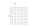
- FIG. 1 is a perspective view showing an example of a microarray device.
- Cross-sectional view B showing an example of a microarray device Plan view B showing an example of a microarray device
- Cross-sectional view C showing an example of a microarray device
- Cross-sectional view D showing an example of a microarray device
- FIG. 1 is a cross-sectional view showing an example of a microarray device.
- FIG. 5 is a cross-sectional view showing an example of a microarray device.
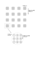
- Cross-sectional view G showing an example of a microarray device Plan view G showing an example of a microarray device A perspective view G showing an example of a microarray device A diagram showing an example of an inspection system.
- Bitmap Pattern Partial
- Bitmap Pattern (Overall) Graph showing the number of microdot light emitters used and the misclassification rate
- the microarray device of the present invention has a plurality of microdot light emitting parts arranged two-dimensionally, and a plurality of microwell structures arranged two-dimensionally. This feature is a technical feature common to or corresponding to each of the following embodiments.
- One embodiment of the microarray device of the present invention includes an organic light-emitting diode, which has a plurality of the microdot light-emitting portions arranged two-dimensionally.
- One embodiment of the microarray device of the present invention includes an organic light-emitting diode, the organic light-emitting diode having an anode, a receiving layer, a cathode, a sealing member, a circuit, and a power receiving section, and the receiving layer having an insulating section and a plurality of the microdot light-emitting sections arranged two-dimensionally.
- One embodiment of the microarray device of the present invention has two or more types of microdot light-emitting parts with different maximum emission wavelengths. This increases wavelength selectivity and explanatory variables, improving the accuracy of data analysis.
- the microdot light-emitting units include at least two types of microdot light-emitting units having a maximum emission wavelength of less than 380 nm, microdot light-emitting units having a maximum emission wavelength of 380 nm or more and less than 500 nm, and microdot light-emitting units having a maximum emission wavelength of 500 nm or more. This further improves the accuracy of data analysis.
- the microdot light-emitting units include at least a microdot light-emitting unit having a maximum emission wavelength of less than 380 nm, a microdot light-emitting unit having a maximum emission wavelength of 380 nm or more and less than 500 nm, and a microdot light-emitting unit having a maximum emission wavelength of 500 nm or more. This further improves the accuracy of data analysis.
- the in-plane coordinates of the microdot light-emitting section and the in-plane coordinates of the microwell structure section at least partially overlap.
- the number of the microdot light-emitting units is greater than the number of the microwell structures, and multiple microdot light-emitting units are located directly below each of the microwell structures. This positional relationship makes it possible to irradiate one microwell structure with excitation light of different wavelengths without using a spectroscopic system. By irradiating one microwell structure 22 with excitation light of different wavelengths, the number of explanatory variables can be increased, improving the accuracy of data analysis.
- the number of the microdot light-emitting sections and the number of the microwell structure sections match, and the in-plane center coordinates of each of the microdot light-emitting sections match the in-plane center coordinates of each of the microwell structure sections.
- One embodiment of the microarray device of the present invention has an insulating portion and a receiving layer having a plurality of the microdot light-emitting portions arranged two-dimensionally, and in the receiving layer, the material of the insulating portion and the material of the microdot light-emitting portion exist with a concentration gradient in the depth direction and in the in-plane direction.
- At least one of the multiple microwell structures contains a sensitizer on the surface. This can improve the sensitivity of data acquisition. Furthermore, by including a sensitizer on the surface, it becomes possible to generate multidimensional data. Specifically, the data generated changes due to interactions such as energy transfer between the specimen and the sensitizer, so data on the molecular structure of the specimen, mixture volume ratio, density, environment, etc. can be generated in a more multidimensional manner.
- At least one of the multiple microwell structures contains a sensitizer on the surface, and the sensitizer uses electromagnetic waves irradiated from the microdot light-emitting section as excitation light to emit one or more of the following types of light: fluorescence, phosphorescence, excimer luminescence, exciplex luminescence, thermally activated delayed fluorescence, excited-state intramolecular proton luminescence, triplet triplet annihilation luminescence, twisted intramolecular charge transfer luminescence, and aggregate organic luminescence. These luminescence mechanisms are suitable for multidimensionalizing generated data.
- At least one of the multiple microwell structures contains a sensitizer on the surface, and the sensitizer is an oligonucleotide.
- the sensitizer is an oligonucleotide.
- Oligonucleotides are preferable as sensitizers because they can be adapted to the shape of the sample. Oligonucleotides are also preferable because, compared to general compounds, the molecular group distance and quantitative ratio can be controlled by block polymerization.
- the method for manufacturing a microarray device of the present invention is a method for manufacturing a microarray device of the present invention, in which the microwell structure is formed by an inkjet method. This allows the microwell structure to be formed easily and quickly.
- the inkjet method is also suitable for forming microwell structures of any shape or minute size.
- the microdot light-emitting sections are formed by an inkjet method. This allows a large number of microdot light-emitting sections to be formed easily and quickly.
- the inkjet method is also suitable for forming microdot light-emitting sections of any shape or minute size.
- the test kit of the present invention is a test kit including a microarray device, and includes the microarray device of the present invention and any one or more of a sensitizer, a specimen, a dropping device, a cover glass, a hardener, a lens, and a microscope.
- the inspection system of the present invention is an inspection system including a microarray device, and includes the microarray device of the present invention, an imaging device, and an analysis device.
- the analysis device extracts RGB data or hyperspectral data from the digital image data generated using the microarray device and the imaging device. This allows for rapid and highly accurate analysis of even large amounts of data or complex data.
- the analysis device uses artificial intelligence to evaluate the condition of the sample. This allows for rapid and highly accurate analysis of even large amounts of data or complex data.
- the testing method of the present invention uses the microarray device of the present invention.
- the microarray device of the present invention has a plurality of microdot light emitting parts arranged two-dimensionally, and a plurality of microwell structures arranged two-dimensionally.
- FIG. 1 is a cross-sectional view showing an example of a microarray device of the present invention.
- the microarray device 100 shown in FIG. 1 includes a sheet-shaped light source unit 10 located on the lower surface of the support 1, and a sheet-shaped multiwell unit 20 located on the upper surface of the support 1.
- the light source unit 10 shown in FIG. 1 is an organic light-emitting diode (OLED).
- the organic light-emitting diode has an anode 11, a receiving layer 19, a cathode 14, a sealing member 15, a barrier material 16, a circuit 17, and a power receiving section 18.
- the receiving layer 19 has an insulating section 12 and a plurality of microdot light-emitting sections 13 arranged two-dimensionally.
- the multiwell unit 20 has a hardened layer 21 and a plurality of microwell structure sections 22 arranged two-dimensionally.
- FIG. 2 is a plan view showing an example of a microarray device of the present invention.
- FIG. 3 is a perspective view showing an example of a microarray device of the present invention.
- electromagnetic waves are irradiated from the microdot light emitter 13, which serves as a light source, to the microwell structure 22, which serves as a reaction site.
- This electromagnetic wave acts as excitation light, causing the specimen present in the microwell structure 22 (or a sensitizer that may be present together with the specimen) to emit light such as fluorescence, generating electromagnetic waves.
- the electromagnetic waves generated from the microwell structure 22 become scientific data on the specimen, substance, or object.
- the microarray device 100 of the present invention has multiple microwell structures 22 that serve as reaction fields, making it possible to generate a large amount of data at once. Also, by having multiple microdot emitters 13 that serve as light sources, the number of microdot emitters 13 for one microwell structure 22 and the positional relationship between the microwell structure 22 and the microdot emitters 13 can be freely adjusted. This makes it possible to change the amount of electromagnetic waves irradiated to each microwell structure 22 and the irradiation angle depending on the microwell structure 22, making it possible to generate a variety of data in a single test. Furthermore, the microarray device 100 of the present invention is easy to handle, making it possible to quickly generate large amounts of data.
- the in-plane coordinates of the microdot light emitter 13 and the in-plane coordinates of the microwell structure 22 can be positioned so that they at least partially overlap. By positioning them in this way, it becomes possible to simultaneously capture the absorption spectrum data and emission spectrum data of the sample during detection. In addition, by positioning them in this way, the optical path length can be shortened, making it possible to provide the microwell structure 13 and the microdot light emitter 22 at a higher density.
- the number of microdot light emitters 13 and the number of microwell structures 22 can be made to match, and the positional relationship can be such that the in-plane center coordinates of each microdot light emitter 13 and the in-plane center coordinates of each microwell structure 22 match.
- the excitation emission efficiency is maximized, thereby improving the accuracy of data analysis.
- the microdot light emitter 13 and the microwell structure 22 can be arranged in a staggered positional relationship. Even in this case, the electromagnetic waves emitted from the microdot light emitter 13 are irradiated onto the microwell structure 22. By adopting such a positional relationship, it is possible to suppress direct detection of the irradiated light from the microdot light emitter 13, which can become noise.
- the number of microdot light emitters 13 can be greater than the number of microwell structures 22, and multiple microdot light emitters 13 can be positioned directly below each microwell structure 22.
- the number of explanatory variables can be increased, and the accuracy of data analysis can be improved.
- the microarray device 100 shown in FIG. 1 is a type that has an organic light-emitting diode as the light source unit 10, but the present invention is not limited to this.
- the support 1 can be one that is transparent to the electromagnetic waves irradiated from the microdot light-emitting section 13.
- the support 1 is not necessary when the multiwell unit 20 is placed directly on the light source unit 10.
- the support 1 is also not necessary when the microdot light-emitting section 13 and the microwell structure section 22 are formed in the same layer or in the same unit.
- the support 1 may be formed by extrusion molding or coating molding of a curable resin such as polyimide or acrylic.
- the support 1 may be in the form of a sheet or may be a three-dimensional support formed by a 3D printer or the like.
- the thickness be less than 1 mm.
- the support 1 can be made of glass, quartz, a transparent resin film, or the like. From the viewpoint of providing flexibility to the microarray device, it is preferable that the support 1 be a resin film.
- resin films include polyesters such as polyethylene terephthalate (PET) and polyethylene naphthalate (PEN), polyethylene, polypropylene, cellophane, cellulose esters or derivatives thereof such as cellulose diacetate, cellulose triacetate (TAC), cellulose acetate butyrate, cellulose acetate propionate (CAP), cellulose acetate phthalate, and cellulose nitrate, polyvinylidene chloride, polyvinyl alcohol, polyethylene vinyl alcohol, syndiotactic polystyrene, polycarbonate, norbornene resin, polymethylpentene, polyether ketone, polyimide, polyether sulfone (PES), polyphenylene sulfide, polysulfones, polyetherimide, polyether ketone imide, polyamide, fluororesin, nylon, polymethyl methacrylate, acrylics or polyarylates, and cycloolefin resins such as Arton (registered trademark) (manuv
- an inorganic gas barrier film, an organic gas barrier film, or an inorganic/organic hybrid gas barrier film may be formed on the surface of the resin film.
- the water vapor permeability (25 ⁇ 0.5°C, relative humidity (90 ⁇ 2)% RH) of the gas barrier film is preferably 0.01 g/( m2 ⁇ 24h) or less, more preferably 10-5 g/( m2 ⁇ 24h) or less.
- the water vapor permeability can be measured by a method conforming to JIS K 7129-1992.
- the oxygen permeability of the gas barrier film is preferably 10-3 mL/( m2 ⁇ 24h ⁇ atm) or less.
- the oxygen permeability can be measured by a method conforming to JIS K 7126-1987.
- the gas barrier film has high barrier properties, with an oxygen permeability of 10 ⁇ 3 mL/(m 2 ⁇ 24 h ⁇ atm) or less and a water vapor permeability of 10 ⁇ 5 g/(m 2 ⁇ 24 h) or less.
- the material from which the gas barrier film is made may be any material that has the function of suppressing the intrusion of moisture, oxygen, etc., which cause deterioration of the element.
- examples of such materials include silicon oxide, silicon dioxide, silicon nitride, etc.
- the method for forming the gas barrier film is not particularly limited.
- methods for forming the gas barrier film include vacuum deposition, sputtering, reactive sputtering, molecular beam epitaxy, cluster ion beam, ion plating, plasma polymerization, atmospheric plasma polymerization, plasma CVD (chemical vapor deposition), laser CVD, thermal CVD, and coating.
- the atmospheric plasma polymerization method described in JP-A-2004-68143 is particularly preferred as a method for forming the gas barrier film.
- the support 1 may be equipped with a filter that converts the wavelength of the electromagnetic waves from the microdot light-emitting unit 13, or a filter that converts the color of the light emitted from the microdot light-emitting unit 13 into multiple colors using a phosphor.
- the microarray device 100 in Fig. 1 has a light source unit 10 which is an organic light emitting diode.
- the light source unit 10 which is an organic light emitting diode has an anode 11, a receiving layer 19, a cathode 14, a sealing member 15, a barrier material 16, a circuit 17, and a power receiving section 18.
- the receiving layer 19 has an insulating section 12 and a microdot light emitting section 13.
- the thickness of the light source unit 10 can be, for example, about 0.2 ⁇ m.
- the anode 11 is preferably made of a metal, alloy, electrically conductive compound, or a mixture thereof having a large work function.
- the work function of the electrode material of the anode 11 is preferably 4 eV or more, more preferably 4.5 V or more.
- Specific examples of such electrode materials include metals such as Au, CuI, indium tin oxide (ITO), SnO 2 , ZnO, and other conductive transparent materials.
- an amorphous material capable of producing a transparent conductive film such as IDIXO (In 2 O 3 -ZnO), may be used.
- a conductive polymer may also be used for the anode 11.
- conductive polymers include PEDOT:PSS, polypyrrole, polyaniline, polythiophene, polythienylenevinylene, polyazulene, polyisothianaphthene, polycarbazole, polyacetylene, polyphenylene, polyphenylenevinylene, polyacene, polyphenylacetylene, polydiacetylene, polynaphthalene, and derivatives thereof. Only one of these electrode materials may be used alone, or two or more materials may be mixed and used. It is also possible to construct an electrode by stacking two or more layers of each material.
- the cathode 14 is preferably made of an electrode material having a small work function (referred to as an electron injecting metal), an alloy, an electrically conductive compound, or a mixture thereof.
- the work function of the electrode material of the cathode 14 is preferably 5 eV or less.
- Specific examples of such electrode materials include sodium, sodium-potassium alloy, magnesium, lithium, silver, a magnesium/copper mixture, a magnesium/silver mixture, a magnesium/aluminum mixture, a magnesium/indium mixture, an aluminum/aluminum oxide (Al 2 O 3 ) mixture, indium, a lithium/aluminum mixture, aluminum, and rare earth metals.
- mixtures of an electron injecting metal and a second metal which has a larger and more stable work function than the electron injecting metal such as a magnesium/silver mixture, a magnesium/aluminum mixture, a magnesium/indium mixture, an aluminum/aluminum oxide ( Al2O3 ) mixture, a lithium/aluminum mixture, and aluminum.
- a transparent or semi-transparent cathode can be produced by depositing a film of the above metal, for example to a thickness of 1 to 20 nm, and then depositing a conductive transparent material on top of it.
- the electrodes are obtained by, for example, forming an electrode material into a thin film by a method such as vapor deposition or sputtering, or by a method such as coating and drying a precursor solution.
- the electrodes (anode 11 and cathode 14) may be provided as a flat film of uniform thickness, or may be provided in a desired pattern shape. In the case of a pattern shape, they can be formed, for example, by a photolithography method, or by an inkjet method for coating a precursor solution. Alternatively, if high pattern precision is not required, they can be formed by vapor deposition or sputtering of the electrode material using a mask of the desired shape.
- the anode 11 is on the microwell structure side, but the cathode 14 may also be on the microwell structure side.
- the electrode on the microwell structure side is preferably transparent or semi-transparent so as to transmit the electromagnetic waves irradiated from the microdot light emitter 13.
- the receiving layer 19 has an insulating portion 12 and a plurality of microdot light emitting portions 13 arranged in a second order.
- the receiving layer 19 is formed by being laminated on at least one of the electrodes (the anode 11 or the cathode 14). It is usually preferable that the receiving layer 19 is formed as a continuous layer.
- the receiving layer 19 is formed so that its entirety is in contact with one of the electrodes.
- the area in which the receiving layer 19 is formed may be, for example, an area that covers the entire surface of the electrode, or an area that covers a specific area of the electrode.
- the constituent material of the insulating portion 12 is preferably at least one type of insulating polymer.
- the "insulating" of the insulating polymer used in the insulating portion 12 means that the electrical resistivity is 1 ⁇ 10 ⁇ m or more, preferably 1 ⁇ 10 ⁇ m or more, and more preferably 1 ⁇ 10 ⁇ m or more.
- the electrical resistivity of the insulating polymer alone is 1 ⁇ 10 ⁇ m or more, leakage current can be suppressed.
- the type of insulating polymer is not particularly limited as long as it is capable of forming the receiving layer 19.
- the insulating polymer is a polymer whose main chain is made up of carbon atoms, which is more stable.
- the insulating polymer is preferably a soluble polymer and preferably exhibits solubility in an aprotic polar solvent.
- the solubility of the insulating polymer in 1.0 g of N,N-dimethylformamide at 25°C is preferably 0.5 mg or more, more preferably 1.0 mg or more, and even more preferably 2.0 mg or more.
- insulating polymers include nonionic polymers such as polystyrene, polymethyl methacrylate, polyvinyl alcohol, polyacrylamide, polyvinylpyrrolidone, polyvinylpolypyrrolidone, polyethylene glycol, polymethyl vinyl ether, and polyisopropylacrylamide; cationic polymers such as sodium polyacrylate, sodium polystyrene sulfonate, sodium polyisopropylene sulfonate, polynaphthalene sulfonic acid condensate salt, and polyethyleneimine xanthate salt; anionic polymers such as dimethylaminomethyl (meth)acrylate quaternary salt, dimethyldiallylammonium chloride, polyamidine, polyvinylimidazoline, dicyandiamide condensate, epichlorohydrin dimethylamine condensate, and polyethyleneimine; and amphoteric polymers such as dimethylaminoethyl (meth)acryl
- the weight-average molecular weight of the insulating polymer is not particularly limited, but is preferably 5 ⁇ 10 3 or more, more preferably 10 ⁇ 10 3 or more. Also, it is preferably 1000 ⁇ 10 3 or less, more preferably 400 ⁇ 10 3 or less. It is considered that the weight-average molecular weight within this range allows the diffusion of the light-emitting compound in the receiving layer 19 to be appropriately controlled.
- the receiving layer 19 may contain other materials and additives.
- additives include halogen elements such as bromine, iodine, and chlorine, halogenated compounds, alkali metals such as Pd, Ca, and Na, alkaline earth metals, and transition metal compounds, complexes, and salts.
- the receiving layer 19 may also contain various functional additives contained in the luminescent ink described below.
- the insulating portion 12 is preferably formed on one of the electrodes (anode 11 or cathode 14) by a wet process.
- wet processes include spin coating, casting, inkjet, die coating, blade coating, roll coating, spray coating, curtain coating, and LB (Langmuir-Blodgett) processes.
- LB Liuir-Blodgett
- a process that is highly suitable for the roll-to-roll process is preferred because it is easy to obtain a homogeneous thin film and has high productivity.
- Processes that are highly suitable for the roll-to-roll process include the die coating, roll coating, inkjet, and spray coating processes.
- the inkjet process is particularly preferred.
- the liquid medium in which the constituent material of the insulating portion 12 is dissolved or dispersed is not particularly limited.
- the liquid medium include halogen-based solvents such as chloroform, carbon tetrachloride, dichloromethane, 1,2-dichloroethane, dichlorobenzene, and dichlorohexanone; ketone-based solvents such as acetone, methyl ethyl ketone, diethyl ketone, methyl isobutyl ketone, n-propyl methyl ketone, and cyclohexanone; aromatic solvents such as benzene, toluene, xylene, mesitylene, and cyclohexylbenzene; aliphatic solvents such as cyclohexane, decalin, and dodecane; ester-based solvents such as ethyl acetate, n-propyl
- the boiling point of these liquid media is preferably lower than the temperature of the drying process in order to quickly dry the liquid media.
- the boiling point of the liquid medium is preferably within the range of 60 to 200°C, and more preferably within the range of 80 to 180°C.
- the coating liquid may contain a surfactant to control the coating area or to suppress the liquid flow caused by the surface tension gradient after coating.
- the liquid flow caused by the surface tension gradient after coating is the liquid flow that causes the phenomenon known as the coffee ring.
- the surfactant is preferably an anionic or nonionic surfactant, for example, from the viewpoint of the effect of moisture contained in the solvent, leveling properties, wettability to the substrate, etc.
- fluorine-containing surfactants, etc., surfactants listed in WO 08/146681, JP 2-41308, etc. can be used.
- the coating liquid used in the wet process may be a solution in which the constituent material of the insulating part 12 is uniformly dissolved in the liquid medium, or a dispersion in which the material is dispersed as a solid in the liquid medium.
- dispersion methods include ultrasonic dispersion, high shear dispersion, and media dispersion.
- the concentration of the coating liquid can be appropriately selected depending on the solubility or dispersibility of the constituent material of the insulating part 12.
- the concentration of the coating liquid can be, for example, within the range of 0.1 to 50%.
- the viscosity of the coating liquid can be appropriately selected depending on the solubility or dispersibility of the material that constitutes the insulating part 12.
- the viscosity of the coating liquid can be, for example, within the range of 0.3 to 100 mPa ⁇ s.
- the thickness of the coating film can be appropriately selected depending on the function required for the insulating portion 12 and the solubility or dispersibility of the constituent materials.
- the thickness of the coating film can be within the range of 1 to 90 ⁇ m, for example.
- a drying process can be performed to remove the liquid medium described above.
- the temperature in the drying process is not particularly limited, but it is preferable to carry out the drying process at a temperature that does not damage the insulating portion 12, electrodes, etc.
- the temperature can be, for example, 80°C or higher, and the upper limit is thought to be around 300°C, although it cannot be generalized as it varies depending on the composition of the coating liquid, etc.
- the drying process time is preferably around 10 seconds to 10 minutes. By adopting such conditions, drying can be carried out quickly.
- a plurality of microdot light emitting units 13 are arranged two-dimensionally.
- Materials constituting the microdot light-emitting section 13 include light-emitting compounds and host compounds.
- the luminescent compound examples include a fluorescent compound, a delayed fluorescent compound, and a phosphorescent compound. From the viewpoint of improving the sensitivity of data acquisition, it is preferable to use a compound that emits blue phosphorescence (a blue phosphorescent luminescent compound).
- the luminescent compound may be a combination of several compounds, such as a combination of different phosphorescent compounds or a combination of a phosphorescent compound and a fluorescent compound. This allows any luminescent color to be obtained.
- the microdot light-emitting unit 13 can also emit white light by containing a plurality of light-emitting compounds with different light-emitting colors.
- the combination of light-emitting compounds that emit white light is not particularly limited, but examples include combinations of blue and orange, blue, green and red, etc.
- the color emitted by a luminescent compound is determined by the color measured using a spectroradiometer CS-1000 (Konica Minolta, Inc.) and applied to the CIE chromaticity coordinates in Figure 3.16 on page 108 of "New Color Science Handbook” (edited by the Color Science Association of Japan, University of Tokyo Press, 1985).
- fluorescent compound refers to a compound that emits fluorescence other than delayed fluorescence.
- Fluorescence refers to light emitted when returning from a singlet excited state to a ground state. Delayed fluorescence will be described later.
- Fluorescent compounds do not necessarily have to be heavy metal complexes like phosphorescent compounds. Fluorescent compounds can be so-called organic compounds that are composed of combinations of common elements such as carbon, oxygen, nitrogen, and hydrogen. Fluorescent compounds may also contain other non-metallic elements such as phosphorus, sulfur, and silicon. Complexes of typical metals such as aluminum and zinc can also be used as fluorescent compounds. In this way, the variety of fluorescent compounds can be said to be almost infinite.
- the fluorescent compound can be appropriately selected from known fluorescent compounds used in the light-emitting layer of an organic EL element.
- fluorescent compounds include anthracene derivatives, pyrene derivatives, chrysene derivatives, fluoranthene derivatives, perylene derivatives, fluorene derivatives, arylacetylene derivatives, styrylarylene derivatives, styrylamine derivatives, arylamine derivatives, boron complexes, coumarin derivatives, pyran derivatives, cyanine derivatives, croconium derivatives, squarium derivatives, oxobenzanthracene derivatives, fluorescein derivatives, rhodamine derivatives, pyrylium derivatives, perylene derivatives, polythiophene derivatives, rare earth complex compounds, polyphenylene derivatives, polyphenylenevinylene derivatives, polythienylenevinylene derivatives, polyaniline derivatives, polyfluorene derivatives, polyvinylcarbazole derivatives, polyarylamine derivatives, etc.
- the term "phosphorescent compound” refers to a compound that emits phosphorescence at room temperature (25° C.) and has a phosphorescence quantum yield of 0.01 or more at 25° C. The phosphorescence quantum yield is preferably 0.1 or more. “Phosphorescence” refers to light emitted when returning from a triplet excited state to the ground state.
- the phosphorescence quantum yield can be measured by the method described in Spectroscopy II, 4th Edition, Experimental Chemistry Lectures 7, p. 398 (1992 edition, Maruzen). There are no limitations on the solvent used for the measurement, and if the phosphorescence quantum yield is 0.01 or more in any solvent, the compound is considered a phosphorescent compound.
- phosphorescence When excited by an electric field, as in an organic EL element, triplet excitons are generated with a 75% probability, and singlet excitons with a 25% probability. Therefore, phosphorescence can achieve a higher luminous efficiency than fluorescence, and is an excellent luminescence method for achieving low power consumption. In terms of luminous efficiency, phosphorescence is theoretically three times more advantageous than fluorescence.
- the phosphorescent compound can be appropriately selected from known compounds used in the light-emitting layer of an organic EL element. Specific examples of known phosphorescent compounds are described in Nature 395, 151 (1998), Appl. Phys. Lett. 78, 1622 (2001), Adv. Mater. 19, 739 (2007), Chem. Mater. 17, 3532 (2005), Adv. Mater. 17,1059 (2005), WO 2009/100991, WO 2008/101842, WO 2003/040257, U.S. Patent Application Publication No. 2006/835469, U.S. Patent Application Publication No. 2006/0202194, U.S. Patent Application Publication No. 2007/0087321, U.S. Patent Application Publication No. 2005/0244673, Inorg.
- organometallic complexes having Ir as the central metal are preferred.
- organometallic complexes containing at least one of the coordination modes of metal-carbon bond, metal-nitrogen bond, metal-oxygen bond, and metal-sulfur bond are more preferred.
- phosphorescent compounds that can be suitably used in the present invention.
- the phosphorescent compounds described in the examples below can also be suitably used in the present invention.
- the term “delayed fluorescent compound” refers to a compound that emits delayed fluorescence.
- “Delayed fluorescence” refers to light emitted when returning from a singlet excited state to a ground state as a result of upconversion caused by reverse intersystem crossing from the lowest excited triplet energy level to the lowest excited singlet energy level. The upconversion occurs when the energy level difference ⁇ E ST between the lowest excited triplet energy level and the lowest excited singlet energy level is extremely small.
- Delayed fluorescence includes thermally activated delayed fluorescence and triplet-triplet annihilation delayed fluorescence.
- delayed fluorescent compounds include thermally activated delayed fluorescent compounds and triplet-triplet annihilation delayed fluorescent compounds.
- thermally activated delayed fluorescent compound refers to a compound that emits thermally activated delayed fluorescence (TADF).
- thermally activated delayed fluorescence (TADF) refers to light emitted when a compound returns from a singlet excited state to a ground state as a result of upconversion from the lowest excited triplet energy level to the lowest excited singlet energy level due to reverse intersystem crossing caused by the absorption of ambient thermal energy.
- TADF thermally activated delayed fluorescence
- thermally activated delayed fluorescent compounds include those described in WO 2011/156793, JP 2011-213643 A, JP 2010-93181 A, Japanese Patent No. 5,366,106, WO 2013/161437, WO 2016/158540, etc.
- the thermally activated delayed fluorescent compound is preferably a compound having a structure represented by the following general formulas (1) to (6).
- Ar 1 to Ar 3 each independently represent a substituted or unsubstituted aryl group. At least one of Ar 1 to Ar 3 represents an aryl group substituted with a group having a structure represented by the following general formula (2)]
- R 1 to R 8 each independently represent a hydrogen atom or a substituent.
- Z represents O, S, O ⁇ C, Ar 4 —N, or a chemical bond.
- Ar 4 represents a substituted or unsubstituted aryl group. Adjacent groups among R 1 to R 8 may form a bond with each other or form a ring via a linking group.
- R 1 to R 5 represents a cyano group
- at least one of R 1 to R 5 represents a group having a structure represented by the following general formula (4)
- the remaining R 1 to R 5 represent a hydrogen atom or a substituent.
- R 21 to R 28 each independently represent a hydrogen atom or a substituent, provided that at least one of the following requirements (A) or (B) is satisfied:
- R 1 and R 2 each independently represent a group having a structure represented by the following general formula (6)]
- R 1 to R 8 each independently represent a hydrogen atom or a substituent.
- Z represents O, S, O ⁇ C, Ar 4 —N, or a bond.
- Ar 4 represents a substituted or unsubstituted aryl group. Adjacent groups among R 1 to R 8 may form a bond with each other or form a ring via a linking group.
- thermally activated delayed fluorescent compounds are listed:
- TTA delayed fluorescence triplet-triplet annihilation delayed fluorescence
- TTA delayed fluorescence triplet-triplet annihilation delayed fluorescence
- T * +T * ⁇ S * +S (In the formula, T * represents a triplet exciton, S * represents a singlet exciton, and S represents a ground state molecule.)
- Known triplet-triplet annihilation delayed fluorescent compounds can be used.
- a host compound is present around the light-emitting compound, since this makes carrier movement smoother and allows for lower voltage.
- the host compound is a compound that transports charges to the light-emitting compound, and light emission by itself is not substantially observed.
- the host compound a compound that has hole transport capability and electron transport capability, prevents the emission wavelength from becoming longer, and has a high glass transition temperature (Tg) is preferred.
- the host compound is preferably a low molecular weight host compound. It is known that when a polymeric host compound is used, the driving voltage generally becomes high (see JP-A-3-171590).
- the proportion of the low molecular weight host is preferably 50% by mass or more of the total host compound, and more preferably 90% by mass or more. At 50% by mass or more, the voltage difference can be reduced, and at 90% by mass or more, the voltage difference can be almost eliminated.
- low molecular weight refers to a molecule with a molecular weight of 2000 or less.
- the host compound may be used alone or in combination with multiple types. By using multiple types of host compounds, it is possible to adjust the transfer of charge.
- the host compound can exist stably in all active species states, including the cation radical state, the anion radical state, and the excited state, and does not undergo chemical changes such as decomposition or addition reactions.
- the host compound has an electron mobility/hole mobility in the range of 0.5 to 2.0, which is the ratio of the electron mobility [cm 2 /(V ⁇ s)] to the hole mobility [cm 2 /(V ⁇ s)].
- the electron mobility [cm 2 /(V ⁇ s)] can be measured by the following method.
- an electron-only device is fabricated.
- the device has a configuration of, for example, an ITO anode/calcium layer/host compound layer/potassium fluoride layer/aluminum cathode.
- the current density-voltage characteristics of the device are obtained.
- the electron mobility can be measured using the current density-voltage characteristics and the space charge limited current equation.
- the hole mobility [cm 2 /(V ⁇ s)] can be measured by the following method.
- a hole-only device is prepared.
- the device has a configuration of, for example, ITO anode/host compound layer/ ⁇ -NPD layer/aluminum cathode.
- the current density-voltage characteristics of the device are obtained.
- the hole mobility can be measured using the current density-voltage characteristics and the space charge limited current equation.
- host compounds are described in JP-A Nos. 2001-257076, 2002-308855, 2001-313179, 2002-319491, 2001-357977, 2002-334786, 2002-8860, and 2002-319491.
- host compounds that can be suitably used in the present invention.
- the host compounds described in the examples below can also be suitably used in the present invention.
- the microdot light emitting sections 13 are preferably formed by the inkjet method. This allows a large number of microdot light emitting sections 13 to be formed easily and quickly.
- the inkjet method is also suitable for forming microdot light emitting sections 13 of any shape or minute size.
- a solution in which a luminescent compound or a host compound is dissolved or dispersed in a solvent (also called “luminescent ink") is dropped onto the insulating part 12.
- concentration of the luminescent compound in the luminescent ink is preferably within the range of 1 to 50 mg/mL.
- Luminous inks can contain various functional additives to improve ejection stability, print head compatibility, storage stability, image storage, and other performance properties.
- various functional additives include viscosity adjusters, surface tension adjusters, resistivity adjusters, film-forming agents, dispersants, surfactants, UV absorbers, antioxidants, anti-fading agents, anti-fungal agents, and anti-rust agents.
- the solvent is not particularly limited as long as it can dissolve or disperse the desired amount of the above material and can eject droplets from an inkjet nozzle.
- solvents include water, alcohols such as methanol, ethanol, propanol, isopropyl alcohol, butanol, hexanol, heptanol, octanol, decanol, cyclohexanol, and terpineol, hydrocarbon compounds such as n-heptane, n-octane, decane, dodecane, tetradecane, toluene, xylene, cymene, durene, indene, dipentene, tetrahydronaphthalene, decahydronaphthalene, and cyclohexylbenzene, and ethylene glycol dimethyl ether, ethylene glycol diethyl ether, ethylene glycol methyl ethyl ether, diethylene glycol dimethyl ether, diethylene glycol diethyl ether, diethylene glycol methyl ethyl ether, 1,2-dimethoxye
- glycol ether ester compounds such as ethylene glycol monomethyl ether acetate, glycol oligomer ether esters such as diethylene glycol monomethyl ether acetate and diethylene glycol monobutyl ether acetate, aliphatic or aromatic esters such as n-propyl acetate, ethyl acetate and propyl benzoate, dicarboxylic acid diesters such as diethyl carbonate, alkoxycarboxylic acid esters such as methyl 3-methoxypropionate and ethyl 3-ethoxypropionate, ketocarboxylic acid esters such as ethyl acetoacetate, and polar compounds such as propylene carbonate, ⁇ -butyrolactone, N-methyl-2-pyrrolidone, dimethylformamide, dimethyl sulfoxide and cyclohexanone.
- glycol ether ester compounds such as ethylene glycol monomethyl ether acetate
- the volume of the luminescent ink droplets when dispensed using the inkjet method is preferably within the range of 1 pL to 1 ⁇ L.
- the size of one microdot light-emitting portion 13 in the in-plane direction is preferably within the range of 30 to 300 ⁇ m when converted into a circular diameter.
- a known inkjet device can be used.
- the IJCS-1 manufactured by Konica Minolta can be used as an inkjet device.
- the head scan speed is preferably a value that allows the dot pitch in the scan direction to be set to an appropriate value.
- the head scan speed is preferably 10 to 200 mm/sec, and more preferably 80 to 100 mm/sec.
- the dot pitch in the scan direction is, for example, 50 to 500 ⁇ m.
- the distance between the ejection nozzles of the head is preferably 50 to 1000 ⁇ m.
- the number of shots required to form one microdot light-emitting section 13 can be set appropriately so that the size of the microdot light-emitting section 13 in the in-plane direction is the desired size.
- Inkjet heads can be, for example, shear mode (piezo) heads or thermal heads.
- Shear mode (piezo) heads have a vibration plate with a piezoelectric element in the ink pressure chamber, and the luminous ink is ejected by the pressure change in the ink pressure chamber caused by this vibration plate.
- Thermal heads have a heating element, and the thermal energy from this heating element causes film boiling of the luminous ink, causing it to be ejected.
- inkjet heads having the configurations described in JP 2012-140017 A, JP 2013-010227 A, JP 2014-058171 A, JP 2014-097644 A, JP 2015-142979 A, JP 2015-142980 A, JP 2016-002675 A, JP 2016-002682 A, JP 2016-107401 A, JP 2017-109476 A, JP 2017-177626 A, etc. can be used.
- the inkjet head is preferably capable of producing droplets at the picoliter level.
- examples of such inkjet heads that can be used include the KM512 and KM1024 manufactured by Konica Minolta.
- the material of the insulating section 12 and the material of the microdot light-emitting section 13 exist in the receiving layer 19 with a concentration gradient in the depth direction and in the in-plane direction.
- Existing with a concentration gradient refers to a state in which the materials exist without a clear boundary between the insulating portion 12 area and the microdot light-emitting portion 13 area.
- this state is achieved by the components of the luminescent ink dissolving part of the components of the insulating portion 12.
- the microdot light-emitting portion 13 may be in the shape of a coffee ring.
- sealing adhesive can be used for the sealing member 15.
- the sealing adhesive include photocurable and heat curable adhesives having reactive vinyl groups such as acrylic acid oligomers and methacrylic acid oligomers, moisture curable adhesives such as 2-cyanoacrylic acid esters, heat and chemical curable (two-part mixture) adhesives such as epoxy adhesives, hot-melt type polyamides, polyesters, polyolefins, and cationic curable ultraviolet curable epoxy resin adhesives.
- sealing adhesive that can be cured at temperatures between room temperature and 80°C.
- the sealing adhesive may contain a desiccant.
- the sealing adhesive may be applied using a dispenser or by printing, such as screen printing.
- the barrier material 16 may be a resin film having a gas barrier film.
- the gas barrier film may be the same as that which the support body may have.
- the circuit 17 is provided to pass electricity from the power receiving portion 18 to the anode 11 and the cathode 14, and the configuration thereof is not particularly limited.
- the power receiving unit 18 is not particularly limited, but may be one capable of receiving power via near field communication (NFC), one capable of receiving power from a battery, one capable of connecting to a power supply cable, or a combination of these, etc. From the viewpoint of miniaturizing the microarray device, it is preferable that the power receiving unit 18 be one capable of receiving power via NFC.
- NFC near field communication
- the multiwell unit 20 has a hardened layer 21 and a plurality of microwell structures 22 arranged two-dimensionally.
- the thickness of the multi-well unit 20 can be, for example, 1 to 100 ⁇ m.
- the multi-well unit 20 can be formed, for example, by applying the material of the hardened layer 21 to areas other than the area that will become the microwell structure 22 on the support 1.
- the application of the material for the hardened layer 21 is preferably performed by an inkjet method, although there is no particular limitation. This allows the multi-well unit 20 and the microwell structure 22 to be formed easily and quickly.
- the inkjet method is also suitable for forming microwell structures 22 of any shape or minute size.
- the inkjet device etc. can be used under the same conditions as for forming the microdot light emitting section 13, for example.
- the material of the cured layer 21 may be composed of, for example, an actinic radiation polymerizable compound and a polymerization initiator. Depending on the type of specimen, an insulating polymer that may constitute the aforementioned receiving layer may also be used as the material of the cured layer 21.
- Actinic ray polymerizable compound refers to a compound that crosslinks or polymerizes when irradiated with actinic rays.
- actinic rays include electron beams, ultraviolet rays, alpha rays, gamma rays, and X-rays. Of the actinic rays, ultraviolet rays and electron beams are preferred.
- actinic ray polymerizable compounds include cationic polymerizable compounds, radical polymerizable compounds, and mixtures thereof. Of the actinic ray polymerizable compounds, radical polymerizable compounds are preferred.
- the actinic ray polymerizable compound may be any of a monomer, a polymerizable oligomer, a prepolymer, and a mixture thereof.
- Radically polymerizable compounds are compounds that have an ethylenically unsaturated double bond group in the molecule. Radical polymerizable compounds can be monofunctional or polyfunctional compounds. Examples of radical polymerizable compounds include various acrylates and methacrylates, which are unsaturated carboxylic acid ester compounds.
- a cationically polymerizable compound is a compound that has a cationically polymerizable group in the molecule.
- Examples of cationically polymerizable compounds include epoxy compounds, vinyl ether compounds, and oxetane compounds.
- the polymerization initiator may be any that can initiate polymerization of an actinic radiation-polymerizable compound.
- the polymerization initiator may be a photoradical initiator.
- the actinic radiation-curable ink contains a cationic polymerizable compound
- the polymerization initiator may be a photocationic initiator (photoacid generator). Note that when the actinic radiation-curable ink can be sufficiently cured without a polymerization initiator, such as when the actinic radiation-curable ink is cured by irradiation with electron beams, a polymerization initiator is not necessary. Any known polymerization initiator may be used.
- the material of the cured layer 21 applied onto the support 1 is cured by irradiation with active rays.
- the active rays to be irradiated can be selected from, for example, electron beams, ultraviolet rays, alpha rays, gamma rays, and X-rays. Irradiation conditions such as irradiation time and illuminance can be appropriately selected depending on the material and thickness of the cured layer 21.
- At least one of the multiple microwell structure portions 22 contains a sensitizer on the surface. This can improve the sensitivity of data acquisition. Furthermore, by including a sensitizer on the surface, it becomes possible to generate multidimensional data. Specifically, the generated data changes due to interactions such as energy transfer between the specimen and the sensitizer, so data on the molecular structure of the specimen, mixture volume ratio, density, environment, etc. can be generated in a more multidimensional manner.
- sensitizers can be used so that different microwell structures 22 contain different sensitizers. This allows data about the sample to be generated in a more multidimensional manner.
- the application of the sensitizer to the microwell structure 22 is preferably carried out by, for example, dispersing or dissolving the sensitizer in a solvent to prepare a sensitizer-containing liquid, and then using an inkjet method.
- the inkjet method allows for precise application to the fine microwell structure 22.
- the light source unit which is an organic light-emitting diode, may have an electron transport layer, a hole blocking layer, an electron injection layer, a hole transport layer, an electron blocking layer, a hole injection layer, etc.
- the layer structure including the electrodes and these layers can be, for example, as follows.
- anode/acceptor layer/cathode ii) anode/acceptor layer/electron transport layer/cathode (iii) anode/hole transport layer/acceptor layer/cathode (iv) anode/hole transport layer/acceptor layer/electron transport layer/cathode (v) anode/hole transport layer/acceptor layer/electron transport layer/electron injection layer/cathode (vi) anode/hole injection layer/hole transport layer/electron blocking layer/acceptor layer/hole blocking layer/electron transport layer/cathode
- Electrode transport layer refers to a layer made of a material that has the function of transporting electrons and that has the function of transmitting electrons injected from the cathode to the receiving layer.
- Examples of materials for the electron transport layer include those described in U.S. Pat. No. 6,528,187, U.S. Pat. No. 7,230,107, U.S. Patent Publication No. 2005/0025993, U.S. Patent Publication No. 2004/0036077, U.S. Patent Publication No. 2009/0115316, U.S. Patent Publication No. 2009/0101870, U.S. Patent Publication No. 2009/0179554, International Publication No. 2003/060956, International Publication No. 2008/132085, Appl. Phys. Lett. 75, 4 (1999), Appl. Phys. Lett. 79, 449 (2001), Appl. Phys. Lett. 81, 162 (2002), Appl.
- hole-blocking layer refers to a layer made of a material that has the ability to transport electrons but has little ability to transport holes.
- the hole-blocking layer can increase the probability of electrons and holes recombining by transporting electrons while blocking holes.
- the materials for the hole blocking layer are preferably the same as those for the electron transport layer described above.
- the “electron injection layer”, also known as the cathode buffer layer, is a layer that is provided between the cathode and the receptor layer to reduce the driving voltage and improve the luminance of emitted light.
- the electron injection layer is described in detail in “Electrode Materials” (pages 123-166) in Chapter 2, Volume 2 of "Organic EL Elements and the Frontier of Their Industrialization” (published by NTS Corporation on November 30, 1998).
- the electron injection layer is preferably provided between the cathode and the receptor layer or between the cathode and the electron transport layer, as necessary.
- hole transport layer refers to a layer made of a material that has the function of transporting holes and that has the function of transmitting holes injected from the anode to the receptor layer.
- the material used in the hole transport layer may have any one of the following properties: hole injection, hole transport, or electron barrier properties.
- hole transport materials include porphyrin derivatives, phthalocyanine derivatives, oxazole derivatives, oxadiazole derivatives, triazole derivatives, imidazole derivatives, pyrazoline derivatives, pyrazolone derivatives, phenylenediamine derivatives, hydrazone derivatives, stilbene derivatives, polyarylalkane derivatives, triarylamine derivatives, carbazole derivatives, indolocarbazole derivatives, isoindole derivatives, acene derivatives such as anthracene and naphthalene, fluorene derivatives, fluorenone derivatives, and polyvinylcarbazole, polymeric materials or oligomers with aromatic amines introduced into the main chain or side chain, polysilane, conductive polymers or oligomers (e.g. PEDOT:PSS, aniline-based copolymers, polyaniline, polythiophene, etc.), etc.
- PEDOT:PSS conductive polymers
- Triarylamine derivatives include benzidine types such as ⁇ -NPD, starburst types such as MTDATA, and compounds with fluorene or anthracene in the triarylamine linking core.
- Hexaazatriphenylene derivatives such as those described in JP-T-2003-519432 and JP-A-2006-135145 can also be used as hole transport materials.
- the hole transport material may be used alone or in combination with multiple types.
- electron blocking layer refers to a layer made of a material that has the ability to transport holes but has little ability to transport electrons.
- the electron blocking layer can increase the probability of electron and hole recombination by blocking electrons while transporting holes.
- the materials for the electron blocking layer are preferably the same as those for the hole transport layer described above.
- the hole injection layer is also described in detail in JP-A-9-45479, JP-A-9-260062, JP-A-8-288069, etc.
- Examples of materials for the hole injection layer include the materials for the hole transport layer described above.
- the microwell structure 22 may be formed in the receiving layer 19, as shown in the cross-sectional views of Figures 7 and 8. Such a microwell structure 22 can be formed by a method of forming it at the same time as forming the receiving layer 19, a method of forming it by drilling holes in the support 1 and the electrode, a method of forming it using a porous material, etc.
- the microdot light-emitting portion 13 is not limited to an organic light-emitting diode light-emitting portion, but may be an inorganic light-emitting diode or a plasma display light-emitting portion.
- Figure 9 is a cross-sectional view of a microarray device 100 in which the light source unit 10 is an inorganic light-emitting diode.
- the microdot light emitter 13 may generate near-infrared light, infrared light, or ultraviolet light.
- the microdot light emitter 13 may be made of PVK, phos, acene, Pt complex thermal deactivator, metal oxide, or composite metal oxide.
- the multiple microdot light-emitting units 13 are two or more types of microdot light-emitting units 13 with different maximum emission wavelengths. This increases the wavelength selectivity and explanatory variables, improving the accuracy of data analysis.
- the multiple microdot light-emitting units 13 preferably include at least two or more of the following: microdot light-emitting units with a maximum emission wavelength of less than 380 nm, microdot light-emitting units with a maximum emission wavelength of 380 nm or more but less than 500 nm, and microdot light-emitting units with a maximum emission wavelength of 500 nm or more, and more preferably include at least all of them. This allows the microarray device 100 to generate data such as that described below, thereby further improving the accuracy of data analysis.
- Electromagnetic waves with wavelengths less than 380 nm contribute, for example, to generating data related to the absorption of excitation light sources and molecular structures.
- Examples of electromagnetic waves in this wavelength range include ultraviolet light with wavelengths of 10 nm or more and less than 380 nm.
- Ultraviolet light includes far ultraviolet light with wavelengths of 10 nm or more and less than 200 nm, and near ultraviolet light with wavelengths of 200 nm or more and less than 380 nm.
- Electromagnetic waves with wavelengths of 380 nm or more and less than 500 nm have a small contribution as an excitation light source for generating emission data of single compounds, for example, but contribute to generating data that emphasizes interactions and excitation and absorption data of cleavage products of conjugated compounds.
- Electromagnetic waves with wavelengths of 500 nm or more contribute to generating data on the absorption of individual compounds, as well as data on aggregates and decomposition products.
- Examples of electromagnetic waves in this wavelength range include green to red visible light with a maximum emission wavelength of 500 nm or more and less than 780 nm, and infrared light with a maximum emission wavelength of 780 nm or more and less than 100 ⁇ m.
- the multiple microdot light-emitting units 13 may generate heat so that the temperature of the microwell structure 22 can be controlled.
- one microwell structure can be provided with one or more microdot light-emitting units. This allows the size, shape, emission wavelength, etc. of the microdot light-emitting unit to be adjusted on demand to suit the sample or sensitizer.
- the light source wavelength, light intensity, temperature, etc. were not controlled for individual wells.
- the microarray device of the present invention can also control the light source wavelength, light intensity, temperature, etc., for individual wells. This makes it possible to intentionally cause chemical or biochemical reactions by exceeding the activation energy of samples or reagents when the purpose is to obtain data for industrial or food processing purposes.
- the arrangement density of the microwell structures 22 is preferably 5/cm2 or more , which enables the miniaturization of the microarray device 100.
- the arrangement density of the microwell structures 22 can be, for example, 5 to 10,000/ cm2 .
- the shape and position of the microwell structure 22 can be freely changed depending on the purpose, such as the structure/fixation of the specimen, centrifugation, light path, reaction path, promotion of drying, prevention of drying, etc.
- the shape of the microwell structure 22 is not limited to a perfect circle, square, hemisphere, square base, etc.
- the shape can be designed to suppress drying of the sample, support, degass, etc., a flow path shape for acquiring reaction time series data or sieve data, a shape suited to light irradiation/removal, etc.
- the size of the microwell structure 22 can be, for example, several tens of ⁇ m depending on the inkjet resolution. Any size larger than that can be freely designed using the input image.
- the method for forming the microwell structure 22 is not limited, but it can be formed by inkjet lamination of a curable resin, 3D printer lamination of a curable resin, laser processing of a resin, photolithography of a curable resin, etc.
- the microwell structure 22 can also be formed by a method of ejecting a solvent into a resin by inkjet to dig holes. Among these, inkjet lamination is preferred because it combines fineness, on-demand properties, and waste-free properties.
- each microwell structure 22 can be different, as shown in the cross-sectional view of FIG. 10, the plan view of FIG. 11, and the perspective view of FIG. 12.
- the sensitizer for example, a compound that improves the visible light imaging sensitivity can be used.
- the compound that improves the visible light imaging sensitivity include the above-mentioned luminescent compounds and compounds that have them as part of their structure. From the viewpoint of enhancing the molecular level interaction with the components contained in the analyte (specimen), it is preferable that the number of aromatic rings, the number of polar substituents, and the number of heteroatoms in these compounds are large. From the same viewpoint, it is also preferable that the number of substituents that cause planar twisting of the interacting rings and steric hindrance of the polar groups and heteroatoms in these compounds is small.
- the sensitizer preferably uses the electromagnetic waves irradiated from the microdot light-emitting section as excitation light to exhibit one or more of the following luminescence: fluorescence, phosphorescence, excimer luminescence, exciplex luminescence, thermally activated delayed fluorescence, excited-state intramolecular proton luminescence, triplet triplet annihilation luminescence, twisted intramolecular charge transfer luminescence, and aggregate organic luminescence. These luminescence mechanisms are suitable for multidimensionalizing the generated data.
- the sensitizer exhibits at least one type of emission selected from fluorescence, excimer emission, and exciplex emission. Furthermore, from the viewpoint of ease of analysis, it is preferable that the sensitizer exhibits at least fluorescence.
- sensitizer for example, those that apply techniques such as polymerization, MOF (metal-organic framework), surface modification of wells or particles, microencapsulation of materials, direct phosphoramidite synthesis extension, PCR (polymerase chain reaction), nanoparticles, etc. can be used.
- MOF metal-organic framework
- PCR polymerase chain reaction
- nanoparticles etc.
- any material that can absorb and/or reflect electromagnetic waves and interact with the specimen can be used, in addition to luminescent materials.
- Oligonucleotides are suitable as sensitizers because they can be adapted to the shape of the sample. Oligonucleotides are also preferable compared to general compounds because the molecular group distance and quantitative ratio can be controlled by block polymerization.
- An oligonucleotide that is preferred as a sensitizer is a compound that has a backbone having one or more structural units that include a pentose- or hexose-derived sugar structure and a phosphate ester bond bound to the sugar structure, and one or more chromophores or luminophores bound to the sugar structure.
- the sugar structure to which the chromophore or luminophore is bound is a ⁇ -form.
- DNA has a structure in which bases are bound to a main chain (deoxyribose) that contains a phosphate ester bond and a structure derived from deoxyribose.
- deoxyribose In natural DNA, all deoxyribose in the main chain is a ⁇ -form. Therefore, if 50% or more of the sugar structure to which the chromophore or luminophore is bound is a ⁇ -form, it can be said that the structure is highly similar to substances that exist in nature, such as DNA and RNA.
- an oligonucleotide in which 50% or more of the sugar structure to which the chromophore or luminophore is bound is a ⁇ -form is effective, especially when the sample is a substance that exists in nature.
- oligonucleotides it is more preferable that 80% or more of the sugar structures to which the chromophore or luminophore is bound are ⁇ -forms, and it is even more preferable that all of them are ⁇ -forms. Whether the sugar structure to which the chromophore or luminophore is bound is ⁇ -form or ⁇ -form can be confirmed by NMR analysis or X-ray crystal structure analysis, etc.
- the main chain of the oligonucleotide may have one or more structural units including a sugar structure derived from a pentose or hexose and a phosphate ester bond bound to the sugar structure.
- the main chain may include only one of the structural units, or may include more than one. That is, the main chain may have one of the sugar structures and one of the phosphate ester bonds bound to the sugar structure, or may have a structure including the sugar structure and the phosphate ester bond alternately.
- both ends of the main chain of the oligonucleotide are sugar structures, so that there is one more sugar structure than the number of phosphate ester bonds.
- the structural units may be the same as or different from each other.
- the number of the structural units contained in the oligonucleotide backbone is appropriately selected depending on the type of sample, etc., but is preferably 2 to 6. As the number of structural units increases, the oligonucleotide is more likely to act specifically on the sample. However, in the present invention, when an oligonucleotide is used as a sensitizer, it is preferable to generate a large amount of data by having the oligonucleotide interact with various positions on the sample. Therefore, it is preferable that the oligonucleotide and the sample have appropriate specificity that is not excessive, and the number of structural units is preferably 6 or less.
- the main chain of the oligonucleotide may partially contain structures other than the structural units containing the pentose or hexose-derived sugar structure and phosphate ester bond, as long as the effect of the present invention is not impaired.
- the structures at both ends of the main chain are not particularly limited, and can be various structures, such as OH groups and alkoxy groups.
- pentoses examples include ribose, deoxyribose, and xylose.
- examples of hexoses include allose, glucose, mannose, etc. If the sugar structure is derived from ribose or deoxyribose, the backbone of the oligonucleotide will have a structure similar to that of DNA or RNA. Therefore, from the viewpoint of facilitating interaction with DNA or RNA, it is preferable that the sugar structure is derived from ribose or deoxyribose.
- the phosphate ester bond is preferably bonded to the carbon at the 3rd position and the carbon at the 5th position of the ribose or deoxyribose.
- the luminophore or chromophore described below is preferably bonded to the 1st position of the ribose or deoxyribose.
- the oligonucleotide preferably contains a structure represented by the following general formula (1a) or (1b).
- Y represents a chromophore or luminophore, as described below.
- the chromophore or luminophore possessed by the oligonucleotide may have a structure that emits a specific type of light by itself in response to a single excitation light, or emits a specific light by the action of multiple chromophores or luminophores.
- the chromophore or luminophore is preferably bound to the sugar structure of the main chain so that the sugar structure is in a ⁇ form.
- chromophore refers to a structure that absorbs light with a wavelength of 300 nm or more.
- “Lumophore” refers to a structure that absorbs light with a wavelength of 300 nm or more and emits light.
- the number of chromophores or luminophores that an oligonucleotide has is not particularly limited, but from the viewpoint that the oligonucleotide is likely to exhibit multiple types of luminescence, it is preferably 2 or more, and more preferably 3 to 6.
- the types may be only one type or two or more types.
- one chromophore or luminophore is usually bound to one sugar structure in the main chain. Therefore, when an oligonucleotide has two or more chromophores or luminophores, it is preferable that the sugar structures in the main chain are also two or more.
- the number of chromophores or luminophores in an oligonucleotide is preferably the same as or less than the number of sugar structures in the main chain described above.
- the number of chromophores or luminophores of an oligonucleotide is less than the number of sugar structures in the backbone, some of the sugar structures are not bound to chromophores or luminophores.
- the sugar structures to which no chromophores or luminophores are bound may not be bound to other atomic groups, but may be bound to natural bases as long as the effect of the present invention is not impaired.
- naturally base refers to adenine, guanine, cytosine, thymine, and uracil.
- the total number of natural bases bound to the sugar structures is preferably 50% or less, more preferably 25% or less, of the total number of sugar structures contained in the backbone.
- the number of natural bases is 50% or less, the association between oligonucleotides is suppressed, and the interaction between the sample and the oligonucleotide tends to be dominant.
- the natural bases and non-natural bases are bound to the sugar structures so that the sugar structures are in the ⁇ form.
- Examples of chromophores or luminophores that emit fluorescence include structures derived from fluorescein, rhodamine, boron dipyrromethene, etc.
- Examples of chromophores or luminophores that emit phosphorescence include structures derived from iridium complexes, platinum complexes, etc.
- Examples of chromophores or luminophores that emit excimer emission include structures derived from pyrene, anthracene, perylene, etc.
- Examples of chromophores or luminophores that emit exciplex emission include structures derived from pyrene-dimethylaniline, etc.
- Examples of chromophores or luminophores that emit thermally activated delayed fluorescence include structures derived from 4CzIPN, DABNA, etc.
- Examples of chromophores or luminophores that emit excited state intramolecular proton emission include structures derived from hydroxyphenylbenzoxazole, etc.
- Examples of chromophores or luminophores that emit triplet triplet annihilation emission include structures derived from 9,10-diphenylanthracene, rubrene, etc.
- Examples of chromophores or luminophores that emit twisted intramolecular charge transfer luminescence include structures derived from diaminoanthracene, diaminonaphthalene, etc.
- Examples of chromophores or luminophores that emit aggregate organic luminescence include structures derived from tetraphenylethene, hexaphenylsilole, etc.
- the molecular weight of the oligonucleotide is appropriately selected depending on the type of chromophore or luminophore possessed by the oligonucleotide, the length of the main chain, etc.
- the molecular weight is preferably 500 to 10,000, and more preferably 100 to 4,000.
- the molecular weight of the oligonucleotide is 10,000 or less, the specificity to the sample is appropriately low, and it is possible to react non-specifically with multiple sites on the sample.
- the above oligonucleotides can be synthesized by the following method. First, prepare a monomer in which a chromophore or luminophore and a phosphate ester are bound to a pentose or hexose. The monomer is polymerized in the desired sequence using the phosphoramidite method with a DNA/RNA synthesizer or the like. This method makes it possible to synthesize a wide variety of oligonucleotides depending on the type of sample.
- a part of the monomer such as a hydroxy group of a sugar structure (e.g., a hydroxy group bonded to the 3rd carbon of ribose or deoxyribose) or a hydroxy group derived from phosphoric acid, is usually supported on a particulate carrier (also referred to as a "carrier particle" in this specification) and a polymerization reaction is carried out.
- a particulate carrier also referred to as a "carrier particle” in this specification
- the carrier particle includes, for example, porous glass or polystyrene.
- the carrier may be removed to obtain only the oligonucleotide, but the oligonucleotide may also be used in a state where it is supported on the carrier particle (also referred to as an "oligonucleotide support" in this specification).
- the surface of the microwell structure 22 may be chemically modified with an inner well surface modifier. This provides the same effect as when the microwell structure 22 contains a sensitizer.
- inner well surface modifiers include polysilazane, polysilazane fluoride, surfactants, and fluorine.
- the specimen is not particularly limited, and various substances and objects can be used as specimens.
- the microarray device of the present invention can be used to evaluate, manage, identify, etc. primary industrial raw materials such as reagents, solutions, mixtures, and food ingredients.
- the microarray device of the present invention can also be used for bioassays such as immunoassays and nucleic acid assays.
- the microarray device of the present invention can also be used to test blood, body fluids, and the like as specimens.
- the microarray device of the present invention can also be used to assure the quality of mixed products such as ink, beverages, seasonings, and preservatives as specimens.
- the microarray device of the present invention can rapidly generate large amounts of scientific data about substances and objects. Therefore, by using the microarray device of the present invention, it is possible to save samples, testing time, and testing reagents, obtain more data, perform multivariate analysis without separation and purification, and simplify the optical system.
- the microarray device of the present invention has a built-in light source, so no optical system is required for the recording device, and images can be easily archived using a smartphone camera, etc. This allows for a wide range of usage scenarios, from primary to secondary industries.
- the test kit according to the present invention includes the microarray device of the present invention and any one or more of a sensitizer, a sample, a dropping device (such as a dropper), a cover glass, a hardener, a lens, and a microscope.
- an inspection system includes the microarray device of the present invention, an imaging device, and an analysis device.
- an imaging device for example, a combination of a photoelectric conversion sensor and an optical device (lens and scanning means) can be used.
- the imaging device may be combined with a loading means, a temperature control means, etc., depending on the case.
- the imaging device may also be combined with an excitation light source separate from the microdot light-emitting unit provided in the microarray device.
- a camera of a smartphone 31 or a combination of this with a microscope lens 32 can also be used.
- An example of an analytical device is a computer capable of running image processing software and data analysis software.
- the analytical device preferably extracts RGB data or hyperspectral data from digital image data generated using a microarray device and an imaging device. This allows for rapid and accurate analysis of large amounts of data or complex data.
- the analytical device preferably uses artificial intelligence to evaluate the condition of the sample. This allows for rapid and highly accurate analysis of large amounts of data or complex data.
- the testing method according to the present invention uses the microarray device of the present invention.
- a sample can be tested in the following manner.
- (4) Using an image recognition script, RGB data or hyperspectral data of the specimen part is obtained.
- the simplest method of acquiring data using the microarray device of the present invention is to convert electromagnetic waves into electrical signals using a photoelectric conversion sensor in sync with excitation light.
- photoelectric conversion sensors include CCD (Charge-Coupled Device) sensors and CMOS (Complementary Metal-Oxide-Semiconductor) sensors.
- CCD Charge-Coupled Device
- CMOS Complementary Metal-Oxide-Semiconductor
- the data converted into electrical signals can be stored on a recording medium, data server, cloud server, etc. Remote data processing is effective when the data acquisition site and the data processing site are different locations.
- Well image data of several million pixels can be obtained as RGB data, emission spectrum data, absorption spectrum data, etc. in a matter of seconds using pattern recognition image processing and scripts.
- Various conditions such as light source wavelength, heat, each inkjet ejection condition, and time series can be added as explanatory variables to the multidimensional and large amount of fingerprint data obtained in this way.
- Testing can be performed without separating the sample, and data-driven analysis can be performed using various data analyses such as regression, principal component analysis, and discriminant analysis, as well as machine learning. Using these methods, it is possible to obtain information for discrimination, prediction, decision-making, etc. by linking it to the physical properties and performance that are the object of the test.
- the target of materials informatics (MI) and process informatics (PI) was the secondary industry.
- DX digital transformation
- the microarray device of the present invention can also be made into a lightweight and extremely thin sheet. By bringing such a microarray device to the site, it is possible to obtain useful data related to multidimensional and large amounts of materials at high density on the spot. In addition, it is possible to process the data remotely via the cloud.
- This method is an important and innovative method that is consistent with the concept of comfortable and safe lives for humanity and the SDGs, represented by decarbonization, and is an excellent method that can be developed into a wide range of applications.
- the data generating system includes, in addition to the above-mentioned inspection system, an inkjet device capable of dispensing a specimen or a sensitizer into a microwell structure of a microarray device.
- the inkjet device preferably includes multiple heads, a liquid exchange delivery system, and ON/OFF image input/output software for the dispensing unit.
- Microarray Devices 101a and 101b and Acquisition of Analysis Data 101 Two microarray devices as shown in Fig. 1 were fabricated according to the following procedure. One was a microarray device 101a containing a sensitizer in the microwell structure, and the other was a microarray device 101b not containing a sensitizer in the microwell structure.
- a gas barrier layer was formed on the entire surface of one side of a polyethylene naphthalate film (manufactured by Teijin DuPont, hereinafter abbreviated as "PEN film”).
- the gas barrier layer was formed using an atmospheric pressure plasma discharge treatment device having a configuration described in JP 2004-68143 A.
- the material of the gas barrier layer was silicon oxide (SiO x ; 1 ⁇ X ⁇ 4).
- the thickness of the gas barrier layer was 500 nm.
- a flexible substrate was produced that had gas barrier properties of an oxygen permeability of 0.001 mL/(m 2 ⁇ 24 h) or less and a water vapor permeability of 0.001 g/(m 2 ⁇ 24 h) or less.
- ITO indium tin oxide
- the support on which the anode was formed was cleaned and lyophilized using an atmospheric pressure plasma discharge treatment device.
- Argon gas was used as the discharge gas
- oxygen gas was used as the reactive gas, supplied at 25°C and 1 L/(min cm).
- the power source used to generate the plasma was a PHF2-K manufactured by Heiden Laboratories, and plasma was generated by applying a voltage of approximately 2 kV.
- an ink 1 for forming an insulating portion having the following composition was ejected by an inkjet method under conditions that the thickness of the layer after drying would be 100 nm so as to cover the entire anode surface.
- an ink 2 for forming an insulating portion was ejected under conditions that the thickness of the layer after drying would be 20 nm.
- a piezo inkjet printer head "KM1024i" manufactured by Konica Minolta was used to eject inks 1 and 2. This formed the insulating portion of the receiving layer.
- inks 1 to 9 for forming a light-emitting portion having the following composition were ejected using an inkjet printer head "KM1024i" in the same manner as described above.
- the bitmap pattern shown in FIG. 14 was used as the input data.
- microdot light-emitting portions 1 to 9 were formed in a circle corresponding to the position of a microwell structure portion having a diameter of 500 ⁇ m, which was to be prepared later, at 60 dpi, every 6 pixels.
- microdot light-emitting portions 1 to 9 were formed in a 3 ⁇ 3 arrangement, at 360 dpi, every 2 pixels, and with a diameter of 100 ⁇ m.
- the dashed circle corresponds to the position of the microwell structure portion.
- the solid circle corresponds to the microdot light-emitting portion.
- the inks 1 to 9 for forming a light-emitting portion contain the following light-emitting dopants (light-emitting compounds) Dp-1 to Dp-9, respectively.
- the insulating portion 2 is dissolved once by the ejected ink, and the luminescent dopant and the host compound in the ink for forming the light-emitting portion are mixed and dried again to form the light-emitting portion.
- the ink was ejected onto the insulating portion under conditions that the layer thickness of the light-emitting portion thus formed would be 30 nm. Next, the ink was dried at 120° C. for 30 minutes under nitrogen to form the microdot light-emitting portion.
- a total of 144 sets of microdot light-emitting sections 1 to 9 were produced in 9 rows and 16 columns.
- the 16 sets in the first row were produced by ejecting only ink 1 for forming the light-emitting section.
- the 16 sets in the second row were produced by ejecting only inks 1 and 2 for forming the light-emitting section.
- the number of inks for forming the light-emitting section was increased to equal the number of rows, and the 16 sets in the ninth row were produced by ejecting all of inks 1 to 9 for forming the light-emitting section.
- the maximum emission wavelengths of the luminescent dopants (luminescent compounds) Dp-1 to Dp-9 are as follows: Dp-1: 477 nm, blue light region Dp-2: 311 nm, ultraviolet region Dp-3: 612 nm, green to red light region Dp-4: 522 nm, green to red light region Dp-5: 347 nm, ultraviolet region Dp-6: 583 nm, green to red light region Dp-7: 362 nm, ultraviolet region Dp-8: 487 nm, blue light region Dp-9: 765 nm, green to red light region
- the extracted anode and cathode were connected to the anode pad and cathode pad of an on-board NCF tag IC: NTAG213F (manufactured by NXP), respectively, to form an anode member.
- the on-board NCF tag IC: NTAG213F was a power receiving antenna that served as a power receiving section.
- ⁇ Preparation of cathode member> (Preparation of cathode film) A separately prepared PEN film was attached to the vacuum deposition apparatus. A tungsten resistance heating boat filled with silver was attached to the vacuum deposition apparatus, and the vacuum chamber was depressurized to 4 ⁇ 10 ⁇ 5 Pa. Thereafter, the boat was energized to heat it, and silver was evaporated to form a cathode having a thickness of 100 nm. The silver surface of the cathode film removed from the vacuum deposition apparatus was spin-coated at 500 rpm with the following ink for forming an electron injection adhesive layer. Then, the film was dried on a hot plate at 120° C. for 10 minutes. Then, the film was cut to a size that could cover the anode and be connected to the extraction electrode to form a cathode film.
- PFN-Br manufactured by Lumtec, molecular weight 10,000
- Branched polyethyleneimine manufactured by Aldrich, molecular weight 10,000
- 2-propanol 1,000 parts by weight
- thermosetting adhesive shown below was uniformly applied to a thickness of 20 ⁇ m along the barrier surface of the substrate using a dispenser. This was dried for 12 hours under a vacuum of 100 Pa or less. Furthermore, the sealing substrate was moved to a nitrogen atmosphere with a dew point temperature of ⁇ 80° C. or less and an oxygen concentration of 0.8 ppm, and dried for 12 hours or more. The moisture content of the sealing adhesive was adjusted to 100 ppm or less.
- thermosetting adhesive an epoxy adhesive made by mixing the following (A) to (C) was used.
- the aforementioned cathode film was placed on the adhesive layer with the cathode surface exposed to form a sealing adhesive member.
- the cathode surface of the sealing adhesive member was placed and adhered to the receptive layer surface including the light-emitting portion of the anode member and the extraction electrode on which the NFC tag was placed.
- a vacuum laminator was used to seal the two together under pressure bonding conditions of a temperature of 90°C and a pressure of 0.1 MPa, forming an OLED substrate.
- the ink for forming the microwell structure having the following composition was ejected at a head heating temperature of 50°C.
- the inkjet printer head "KM1024i" was used for the ejection as described above.
- the bitmap patterns shown in Figs. 14 and 15 were used as input data. According to these bitmap patterns, the outside of the circle was solid-colored so that the inside of the circle of 60 dpi, 6 pixels, and 500 ⁇ m in diameter was left blank.
- the ejection was performed twice by changing the inkjet printing scanning direction by 90°.
- the ink was cured by irradiating with a UV-LED with an illuminance of 2000 mW/ cm2 for 10 seconds, and the thickness of the flat part after curing was 10 um.
- the hole portion surrounded by the cured composition is the microwell structure.
- the layer of the cured composition is the cured layer.
- ⁇ Ink for forming microwell structure Diphenyl(2,4,6-trimethylbenzoyl)phosphine oxide (Sigma-Aldrich): 2 parts by weight 2-phenoxyethyl acrylate (TCI): 45 parts by weight Phenoxydiethylene glycol acrylate (Shin-Nakamura Chemical): 45 parts by weight Polyacrylic acid (Sigma-Aldrich, molecular weight 450,000): 8 parts by weight
- the crude product containing intermediate 3 was mixed with THF (100 mL), 1 M tetrabutylammonium fluoride THF solution (117 mL, 117 mmol), and acetic acid (6.74 mL, 117 mmol), and stirred at 40°C for 2 hours. Water was added to stop the reaction, and separation and extraction were performed with ethyl acetate. The resulting organic phase was dried over magnesium sulfate, and the solvent was distilled off to obtain a crude product, which was purified by silica gel column chromatography to obtain the desired intermediate 4 as a light brown solid (5.87 g, 63%).
- sensitizer-containing solutions 1-16 containing each of sensitizers 1-16 were dried using a centrifugal dryer, and ultrapure water was added to obtain sensitizer-containing solutions 1-16 containing each of sensitizers 1-16. It was confirmed that the sensitizers 1-16 emit fluorescence and excimer emission when exposed to specific excitation light (light with a wavelength of 350 nm).
- Sensitizer-containing solutions 1 to 16 were ejected into the 9-row, 16-column microwell structures, sensitizer 1 was ejected into all microwell structures in column 1, and similarly, corresponding sensitizers were ejected up to column 16. This was designated microarray device 101a. Sensitizer-containing solutions 1 to 16 were ejected using a piezo inkjet printer head "KM1024a" manufactured by Konica Minolta. In addition, the other of the two microarray devices produced was not ejected with the sensitizer-containing solution, and was designated microarray device 101b.
- ⁇ Data Acquisition> (Acquisition of luminescence images)
- the power receiving antenna of the microarray device 101a was held over a USB-powered non-contact IC card reader PaSoRi RC-S300 (manufactured by Sony Corporation) to cause the microdot light emitting part to emit light.
- An image was taken from above the microarray part of the microarray device 101a using a microscope, and a PNG format image 101a was obtained.
- the image 101a was subjected to OpenCV, an open source image processing library, to detect the contour of the outer periphery of each microwell structure, and the RGB values of the center of gravity of the detected contour were obtained.
- RGB values were obtained in the same manner.
- the analytical accuracy was greatly improved by increasing the number of microdot light-emitting elements used from one to two, and by using two or more types of microdot light-emitting elements among those with a maximum emission wavelength of less than 380 nm, those with a maximum emission wavelength of 380 nm or more but less than 500 nm, and those with a maximum emission wavelength of 500 nm or more.
- the number of microdot light-emitting elements used was increased from two to three, and it was found that the analysis accuracy was greatly improved by having all the microdot light-emitting elements, including those with a maximum emission wavelength of less than 380 nm, those with a maximum emission wavelength of 380 nm or more but less than 500 nm, and those with a maximum emission wavelength of 500 nm or more.
- the above-mentioned microarray device enables high-density, multi-dimensional analysis of the interaction state between the sample and the sensitizer using a simple process and energy-saving detection method that utilizes a CMOS sensor of a general-purpose camera, etc.
- the present invention can be used in a microarray device capable of rapidly generating large amounts of scientific data about substances and objects, a method for manufacturing the microarray device, and a test kit, test system, and test method that use the microarray device.
- Microarray device 100 Microarray device 1 Support 10 Light source unit 11 Anode 12 Insulating section 13 Microdot light emitting section 14 Cathode 15 Sealing member 16 Barrier material 17 Circuit 18 Power receiving section 19 Receptive layer 20 Multiwell unit 21 Hardened layer 22 Microwell structure section 31 Smartphone 32 Microscope lens
Landscapes
- Health & Medical Sciences (AREA)
- Physics & Mathematics (AREA)
- Life Sciences & Earth Sciences (AREA)
- Chemical & Material Sciences (AREA)
- Analytical Chemistry (AREA)
- Biochemistry (AREA)
- General Health & Medical Sciences (AREA)
- General Physics & Mathematics (AREA)
- Immunology (AREA)
- Pathology (AREA)
- Nuclear Medicine, Radiotherapy & Molecular Imaging (AREA)
- Measuring Or Testing Involving Enzymes Or Micro-Organisms (AREA)
Priority Applications (1)
| Application Number | Priority Date | Filing Date | Title |
|---|---|---|---|
| JP2024561257A JPWO2024116670A1 (https=) | 2022-11-30 | 2023-10-26 |
Applications Claiming Priority (2)
| Application Number | Priority Date | Filing Date | Title |
|---|---|---|---|
| JP2022-191269 | 2022-11-30 | ||
| JP2022191269 | 2022-11-30 |
Publications (1)
| Publication Number | Publication Date |
|---|---|
| WO2024116670A1 true WO2024116670A1 (ja) | 2024-06-06 |
Family
ID=91323719
Family Applications (1)
| Application Number | Title | Priority Date | Filing Date |
|---|---|---|---|
| PCT/JP2023/038711 Ceased WO2024116670A1 (ja) | 2022-11-30 | 2023-10-26 | マイクロアレイデバイス、マイクロアレイデバイスの製造方法、検査キット、検査システム、及び検査方法 |
Country Status (2)
| Country | Link |
|---|---|
| JP (1) | JPWO2024116670A1 (https=) |
| WO (1) | WO2024116670A1 (https=) |
Cited By (1)
| Publication number | Priority date | Publication date | Assignee | Title |
|---|---|---|---|---|
| CN119985967A (zh) * | 2025-04-15 | 2025-05-13 | 密码子(杭州)科技有限公司 | 一种生物芯片点样方法及点样装置 |
Citations (9)
| Publication number | Priority date | Publication date | Assignee | Title |
|---|---|---|---|---|
| JP2002189026A (ja) * | 2000-08-25 | 2002-07-05 | Stmicroelectronics Srl | Dnaマイクロアレイのイメージなどを自動解析するシステム |
| JP2016534723A (ja) * | 2013-10-22 | 2016-11-10 | キム・ソンチョン | 生体分子と核酸の結合情報を生成するためのマーカー、その製造方法、並びにそれを用いた生体分子分析方法及び装置 |
| JP2018516541A (ja) * | 2015-04-14 | 2018-06-28 | コーニンクレッカ フィリップス エヌ ヴェKoninklijke Philips N.V. | 生物学的組織試料の分子プロファイルの空間マッピング |
| WO2020054562A1 (ja) * | 2018-09-11 | 2020-03-19 | ウシオ電機株式会社 | マイクロプレートリーダー |
| WO2021111898A1 (ja) * | 2019-12-06 | 2021-06-10 | コニカミノルタ株式会社 | 有機エレクトロルミネッセンス素子、その製造方法及び表示装置 |
| WO2021202264A1 (en) * | 2020-03-29 | 2021-10-07 | Agilent Technologies, Inc. | Systems and methods for electronically and optically monitoring biological samples |
| JP2021533830A (ja) * | 2018-08-17 | 2021-12-09 | エンリッチ セラピューティクス インコーポレイテッド | 粒子および細胞を選択かつ単離するシステムおよび方法ならびにその使用 |
| JP2022099677A (ja) * | 2020-12-23 | 2022-07-05 | コニカミノルタ株式会社 | 有機エレクトロルミネッセンス素子、その製造方法、表示装置及び照明装置 |
| WO2023171738A1 (ja) * | 2022-03-10 | 2023-09-14 | コニカミノルタ株式会社 | 解析システム、プレート、および解析方法 |
-
2023
- 2023-10-26 WO PCT/JP2023/038711 patent/WO2024116670A1/ja not_active Ceased
- 2023-10-26 JP JP2024561257A patent/JPWO2024116670A1/ja active Pending
Patent Citations (9)
| Publication number | Priority date | Publication date | Assignee | Title |
|---|---|---|---|---|
| JP2002189026A (ja) * | 2000-08-25 | 2002-07-05 | Stmicroelectronics Srl | Dnaマイクロアレイのイメージなどを自動解析するシステム |
| JP2016534723A (ja) * | 2013-10-22 | 2016-11-10 | キム・ソンチョン | 生体分子と核酸の結合情報を生成するためのマーカー、その製造方法、並びにそれを用いた生体分子分析方法及び装置 |
| JP2018516541A (ja) * | 2015-04-14 | 2018-06-28 | コーニンクレッカ フィリップス エヌ ヴェKoninklijke Philips N.V. | 生物学的組織試料の分子プロファイルの空間マッピング |
| JP2021533830A (ja) * | 2018-08-17 | 2021-12-09 | エンリッチ セラピューティクス インコーポレイテッド | 粒子および細胞を選択かつ単離するシステムおよび方法ならびにその使用 |
| WO2020054562A1 (ja) * | 2018-09-11 | 2020-03-19 | ウシオ電機株式会社 | マイクロプレートリーダー |
| WO2021111898A1 (ja) * | 2019-12-06 | 2021-06-10 | コニカミノルタ株式会社 | 有機エレクトロルミネッセンス素子、その製造方法及び表示装置 |
| WO2021202264A1 (en) * | 2020-03-29 | 2021-10-07 | Agilent Technologies, Inc. | Systems and methods for electronically and optically monitoring biological samples |
| JP2022099677A (ja) * | 2020-12-23 | 2022-07-05 | コニカミノルタ株式会社 | 有機エレクトロルミネッセンス素子、その製造方法、表示装置及び照明装置 |
| WO2023171738A1 (ja) * | 2022-03-10 | 2023-09-14 | コニカミノルタ株式会社 | 解析システム、プレート、および解析方法 |
Cited By (1)
| Publication number | Priority date | Publication date | Assignee | Title |
|---|---|---|---|---|
| CN119985967A (zh) * | 2025-04-15 | 2025-05-13 | 密码子(杭州)科技有限公司 | 一种生物芯片点样方法及点样装置 |
Also Published As
| Publication number | Publication date |
|---|---|
| JPWO2024116670A1 (https=) | 2024-06-06 |
Similar Documents
| Publication | Publication Date | Title |
|---|---|---|
| JP5499972B2 (ja) | 有機エレクトロルミネッセンス素子用材料、および有機エレクトロルミネッセンス素子、これを用いた表示装置、照明装置 | |
| Bai et al. | Predicting dexter energy transfer interactions from molecular orbital overlaps | |
| JP5387563B2 (ja) | 有機エレクトロルミネッセンス素子材料、有機エレクトロルミネッセンス素子、有機エレクトロルミネッセンス素子の製造方法、照明装置及び表示装置 | |
| JP5783007B2 (ja) | 有機エレクトロルミネッセンス素子および照明装置 | |
| JP5653617B2 (ja) | 有機エレクトロルミネッセンス素子、有機エレクトロルミネッセンス素子材料、表示装置及び照明装置 | |
| Zhu et al. | Ultrahighly efficient white quantum dot light‐emitting diodes operating at low voltage | |
| US9257651B2 (en) | Organic electroluminescence element and method for manufacturing organic electroluminescence element | |
| JP6424626B2 (ja) | 有機エレクトロルミネッセンス素子、照明装置及び表示装置 | |
| JP5423363B2 (ja) | 有機エレクトロルミネッセンス素子、表示装置及び照明装置 | |
| Wang et al. | Color conversion efficiency enhancement of colloidal quantum dot through its linkage with synthesized metal nanoparticle on a blue light-emitting diode | |
| WO2024116670A1 (ja) | マイクロアレイデバイス、マイクロアレイデバイスの製造方法、検査キット、検査システム、及び検査方法 | |
| Liao et al. | Optical fingerprint classification of single upconversion nanoparticles by deep learning | |
| Ma et al. | Multi-color light-emitting diodes | |
| Liu et al. | Depolymerizable and recyclable luminescent polymers with high light-emitting efficiencies | |
| Meng et al. | Unconventional, gram-scale synthesis of a molecular dimer organic luminogen with aggregation-induced emission | |
| Jagadhane et al. | Multifunctional fluorescent tetraphenylethene-based reversible mechanochromism for highly selective detection of MnO4–in aqueous media and green organic light emitting diode applications | |
| Leng et al. | Unraveling the mechanism of near-infrared thermally activated delayed fluorescence of TPA-based molecules: Effect of hydrogen bond steric hindrance | |
| Galisteo-López et al. | Nanophotonics for current and future white light-emitting devices | |
| Bezvikonnyi et al. | Derivatives of imidazole and carbazole as bifunctional materials for organic light-emitting diodes | |
| Polgar et al. | Enhancement of red thermally assisted fluorescence in bottlebrush block copolymers | |
| WO2025022794A1 (ja) | 解析装置、および解析方法 | |
| Martin et al. | Simple donor–acceptor luminogen based on an azaindole derivative as solid-state emitter for organic light-emitting devices | |
| Celestino et al. | Tuning nonradiative lifetimes via molecular aggregation | |
| Zhang et al. | Layer-by-layer assembly of stable aqueous quantum dots for luminescent planar plate | |
| JP5803692B2 (ja) | 有機エレクトロルミネッセンス素子及び照明装置 |
Legal Events
| Date | Code | Title | Description |
|---|---|---|---|
| 121 | Ep: the epo has been informed by wipo that ep was designated in this application |
Ref document number: 23897326 Country of ref document: EP Kind code of ref document: A1 |
|
| WWE | Wipo information: entry into national phase |
Ref document number: 2024561257 Country of ref document: JP |
|
| NENP | Non-entry into the national phase |
Ref country code: DE |
|
| 122 | Ep: pct application non-entry in european phase |
Ref document number: 23897326 Country of ref document: EP Kind code of ref document: A1 |