WO2024116412A1 - 半導体製造装置用部材 - Google Patents
半導体製造装置用部材 Download PDFInfo
- Publication number
- WO2024116412A1 WO2024116412A1 PCT/JP2022/044618 JP2022044618W WO2024116412A1 WO 2024116412 A1 WO2024116412 A1 WO 2024116412A1 JP 2022044618 W JP2022044618 W JP 2022044618W WO 2024116412 A1 WO2024116412 A1 WO 2024116412A1
- Authority
- WO
- WIPO (PCT)
- Prior art keywords
- plug
- thread
- gas
- ceramic plate
- semiconductor manufacturing
- Prior art date
- Legal status (The legal status is an assumption and is not a legal conclusion. Google has not performed a legal analysis and makes no representation as to the accuracy of the status listed.)
- Ceased
Links
Images




Classifications
-
- H—ELECTRICITY
- H10—SEMICONDUCTOR DEVICES; ELECTRIC SOLID-STATE DEVICES NOT OTHERWISE PROVIDED FOR
- H10P—GENERIC PROCESSES OR APPARATUS FOR THE MANUFACTURE OR TREATMENT OF DEVICES COVERED BY CLASS H10
- H10P72/00—Handling or holding of wafers, substrates or devices during manufacture or treatment thereof
- H10P72/70—Handling or holding of wafers, substrates or devices during manufacture or treatment thereof for supporting or gripping
Definitions
- the present invention relates to components for semiconductor manufacturing equipment.
- a semiconductor manufacturing device component that includes a ceramic plate having a wafer mounting surface on the upper surface, a plug placement hole that penetrates the ceramic plate in the vertical direction, a plug placed in the plug placement hole, a base plate provided on the lower surface of the ceramic plate, and a gas supply path provided in the base plate.
- Patent Document 1 discloses a structure in which a male thread is provided on the outer peripheral surface of the plug and a female thread is provided on the inner peripheral surface of the plug placement hole, the plug is screwed into the plug placement hole, and gas is supplied from the gas supply path to the wafer mounting surface via the plug.
- the plug screwed into the plug placement hole has a hole that penetrates in the vertical direction, and gas is supplied from the gas supply path to the wafer mounting surface via the hole.
- the plug screwed into the plug placement hole is made of a porous material, and gas is supplied from the gas supply path to the wafer mounting surface via pores present inside. Such a plug can be easily attached and removed by the screw.
- Patent Document 1 when a hole penetrating in the vertical direction is provided in the plug, the distance from the wafer mounting surface to the base plate is short, so the withstand voltage is low and arc discharge can occur through the hole when the wafer is processed with plasma. Also, when the plug is made porous, there are many pores inside the plug, so the withstand voltage is also low and arc discharge can occur through the pores when the wafer is processed with plasma.
- the present invention was made to solve these problems, and its main purpose is to suppress the occurrence of arc discharge in semiconductor manufacturing equipment components equipped with threaded plugs.
- the semiconductor manufacturing equipment member of the present invention comprises: a ceramic plate having a wafer mounting surface on an upper surface thereof; a plug arrangement hole that passes through the ceramic plate in the vertical direction and has an internal thread on an inner circumferential surface; a dense plug having an external thread on an outer circumferential surface thereof and screwed into the internal thread of the plug placement hole; a gas passage provided between the female thread of the plug placement hole and the male thread of the dense plug, the gas passage communicating from the lower surface to the upper surface of the ceramic plate; a conductive base plate bonded to a lower surface of the ceramic plate via a bonding layer; a gas supply path provided in the base plate and the bonding layer for supplying a gas to the gas passage; It is equipped with the following:
- the dense plug is screwed into the plug placement hole, so that if the dense plug needs to be replaced, it can be easily replaced.
- gas is supplied from the gas supply path to the wafer mounting surface via a gas passage between the female thread of the plug placement hole and the male thread of the dense plug, rather than via the dense plug. Because the gas passage is a spiral passage formed along the thread, the creepage distance from the wafer mounting surface to the base plate can be increased. This increases the withstand voltage, making it possible to suppress the occurrence of arc discharge through the gas passage when processing the wafer with plasma.
- up/down, left/right, front/back are merely relative positional relationships. Therefore, when the orientation of a semiconductor manufacturing equipment component is changed, up/down may become left/right and left/right may become up/down, but such cases are also within the technical scope of this invention.
- At least one of the female thread and the male thread may be provided with a deeper valley than the dimension specified by the standard. In this way, the flow rate of gas flowing through the gas passage can be increased.
- At least one of the female thread and the male thread may be provided with a lower crest height than the dimensions specified by the standard. This also makes it possible to increase the flow rate of gas flowing through the gas passage.
- the maximum length of the gas passage in the vertical direction may be 0.5 mm or less. If the maximum length of the gas passage in the vertical direction is 0.5 mm or less, it is possible to suppress the occurrence of abnormal discharge (glow discharge) in the gas passage when processing a wafer with plasma.
- FIG. 2 is a longitudinal sectional view of a semiconductor manufacturing equipment member 10.
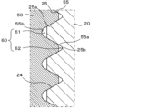
- FIG. FIG. 2 is a partially enlarged view of the female thread 25 and the male thread 55 in FIG. 1 .
- FIG. 13 is a partially enlarged view of another example of the female thread 25 and the male thread 55.
- FIG. 13 is a partially enlarged view of another example of the female thread 25 and the male thread 55.
- FIG. 13 is a partially enlarged view of another example of the female thread 25 and the male thread 55.
- FIG. 13 is a partially enlarged view of another example of the female thread 25 and the male thread 55.
- FIG. 2 is a longitudinal sectional view of a semiconductor manufacturing equipment member 110.
- FIG. 1 is a vertical cross-sectional view of a semiconductor manufacturing equipment member 10
- FIG. 2 is a plan view of a ceramic plate 20
- FIG. 3 is an enlarged view of the female thread 25 and male thread 55 in FIG. 1 (an enlarged view of the area surrounded by the two-dot chain line in FIG. 1).
- the semiconductor manufacturing equipment component 10 includes a ceramic plate 20, a plug placement hole 24, a base plate 30, a dense plug 50, and a gas passage 60.
- the ceramic plate 20 is a ceramic circular plate (e.g., 300 mm in diameter, 5 mm in thickness) made of alumina sintered body or aluminum nitride sintered body.
- the upper surface of the ceramic plate 20 is the wafer mounting surface 21.
- the ceramic plate 20 has an electrode 22 built in.
- the wafer mounting surface 21 of the ceramic plate 20 has a seal band 21a formed along the outer edge, and a plurality of circular small protrusions 21b formed on the entire surface.
- the seal band 21a and the circular small protrusions 21b have the same height, for example, several ⁇ m to several tens of ⁇ m.
- the electrode 22 is a flat mesh electrode used as an electrostatic electrode, and a DC voltage can be applied to it.
- the wafer W When a DC voltage is applied to the electrode 22, the wafer W is attracted and fixed to the wafer mounting surface 21 (specifically, the upper surface of the seal band 21a and the upper surface of the circular small protrusions 21b) by electrostatic attraction force, and when the application of the DC voltage is released, the wafer W is released from the wafer mounting surface 21.
- the portion of the wafer mounting surface 21 on which the seal band 21a and small circular protrusions 21b are not provided is referred to as the reference surface 21c.
- the plug arrangement hole 24 is a through hole that penetrates the ceramic plate 20 in the vertical direction and faces the gas hole 34 of the base plate 30.
- the plug arrangement hole 24 penetrates the electrode 22 in the vertical direction, but the electrode 22 is not exposed on the inner surface of the plug arrangement hole 24.
- the plug arrangement hole 24 has a female thread 25 on its inner surface.
- the plug arrangement hole 24 is provided in multiple locations on the ceramic plate 20 (e.g., multiple locations equally spaced along the circumferential direction).
- the base plate 30 is a circular plate with good thermal conductivity (a circular plate with the same diameter as or larger than the ceramic plate 20). Inside the base plate 30, a refrigerant flow path 32 in which a refrigerant (e.g., an electrically insulating liquid such as a fluorine-based inert liquid) circulates and a gas hole 34 for supplying gas to the gas passage 60 are formed.
- a refrigerant e.g., an electrically insulating liquid such as a fluorine-based inert liquid
- the gas hole 34 is provided so as to penetrate the base plate 30 in the vertical direction.
- the refrigerant flow path 32 is formed in a single line from the inlet to the outlet over the entire surface of the base plate 30 in a plan view.
- materials for the base plate 30 include metals and composite materials. Examples of metals include Al, Al alloys, and Mo.
- composite materials include composite materials of metal and ceramic.
- composite materials of metal and ceramic include metal matrix composite materials (metal matrix composites (MMC)) and ceramic matrix composite materials (ceramic matrix composites (CMC)).
- MMC metal matrix composites
- CMC ceramic matrix composites
- Specific examples of such composite materials include materials containing Si, SiC, and Ti, and materials in which a porous SiC body is impregnated with Al and/or Si.
- a material containing Si, SiC, and Ti is called SiSiCTi
- AlSiC a material in which a porous SiC body is impregnated with Al
- SiSiC a material in which a porous SiC body is impregnated with Si.
- the base plate 30 is also used as an RF electrode. Specifically, an upper electrode (not shown) is disposed above the wafer mounting surface 21, and when high-frequency power is applied between the parallel plate electrodes consisting of the upper electrode and the base plate 30, plasma is generated.
- the metal bonding layer 40 bonds the lower surface of the ceramic plate 20 to the upper surface of the base plate 30.
- the metal bonding layer 40 is formed, for example, by TCB (thermal compression bonding).
- TCB refers to a known method in which a metal bonding material is sandwiched between two members to be bonded, and the two members are pressure-bonded while being heated to a temperature below the solidus temperature of the metal bonding material.
- the metal bonding layer 40 may be a layer formed of solder or a metal brazing material.
- the metal bonding layer 40 has a through hole 42.
- the through hole 42 is formed to a size that includes the plug arrangement hole 24 in a plan view, and is connected to the gas hole 34.
- the gas hole 34 and the through hole 42 correspond to the gas supply path of the present invention.
- the dense plug 50 is an electrically insulating cylindrical member through which gas cannot pass. As shown in FIG. 3, a male thread 55 is provided on the outer peripheral surface of the dense plug 50. The male thread 55 of the dense plug 50 is screwed into the female thread 25 of the plug arrangement hole 24.
- FIG. 3 shows an example in which a standardized general metric thread (JIS B 0205) is used as the female thread 25 and the male thread 55.
- JIS B 0205 standardized general metric thread
- the upper surface of the dense plug 50 is located lower than the upper surface of the seal band 21a and the upper surface of the small circular protrusion 21b. In this embodiment, the upper surface of the dense plug 50 is at the same height as the reference surface 21c of the wafer mounting surface 21.
- the overall length of the dense plug 50 is the same as the overall length of the plug arrangement hole 24.
- a ceramic dense body can be used as the dense plug 50.
- a dense body made of the same material as the ceramic plate 20 can be used as the ceramic dense body.
- the gas passage 60 is provided between the female thread 25 of the plug placement hole 24 and the male thread 55 of the dense plug 50, and communicates from the lower surface to the upper surface (wafer mounting surface 21) of the ceramic plate 20.
- the gas passage 60 is composed of a gap 61 between the crest 25a of the female thread 25 with a trapezoidal cross section and the valley 55b of the male thread 55 with a circular arc cross section (R-shaped), and a gap 62 between the valley 25b of the female thread 25 with a circular arc cross section (R-shaped) and the crest 55a of the male thread 55 with a trapezoidal cross section.
- the gap 61 is formed in a spiral shape along the valley 55b of the male thread 55 so as to communicate from the lower surface to the upper surface (wafer mounting surface 21) of the ceramic plate 20.
- the gap 62 is formed in a spiral shape along the valley 25b of the female thread 25 so as to communicate from the lower surface to the upper surface (wafer mounting surface 21) of the ceramic plate 20.
- the semiconductor manufacturing equipment member 10 is installed in a chamber (not shown), and the wafer W is placed on the wafer placement surface 21. Then, the chamber is depressurized by a vacuum pump to adjust the chamber to a predetermined vacuum level, and a DC voltage is applied to the electrode 22 of the ceramic plate 20 to generate an electrostatic adsorption force, and the wafer W is adsorbed and fixed to the wafer placement surface 21 (specifically, the upper surface of the seal band 21a or the upper surface of the circular small protrusion 21b).
- the chamber is made into a reactive gas atmosphere with a predetermined pressure (for example, several tens to several hundreds of Pa), and in this state, a high-frequency voltage is applied between an upper electrode (not shown) provided on the ceiling part of the chamber and the base plate 30 of the semiconductor manufacturing equipment member 10 to generate plasma.
- a coolant is circulated through the coolant flow path 32 of the base plate 30.
- a backside gas is introduced into the gas hole 34 from a gas cylinder (not shown).
- a thermally conductive gas for example, helium
- the backside gas is supplied and sealed in the space between the back surface of the wafer W and the reference surface 21c of the wafer mounting surface 21 through the gas holes 34, the through holes 42, and the gas passages 60.
- the presence of this backside gas ensures efficient thermal conduction between the wafer W and the ceramic plate 20.
- the backside gas does not pass through the dense plug 50 itself.
- the ceramic plate 20 and the dense plug 50 are prepared.
- the ceramic plate 20 and the dense plug 50 are as already described.
- the dense plug 50 is screwed into the plug arrangement hole 24 of the ceramic plate 20.
- an adhesive knob is attached to the upper or lower surface of the dense plug 50, and the knob is picked up by hand to screw the dense plug 50 into the upper or lower opening of the plug arrangement hole 24.
- the dense plug 50 is screwed so that the upper surface of the dense plug 50 coincides with the reference surface 21c of the wafer mounting surface 21.
- the dense plug 50 is screwed into the plug placement hole 24, so that the dense plug 50 can be easily replaced when it becomes necessary to replace it.
- gas is supplied from the gas hole 34 to the wafer mounting surface 21 through a gas passage 60 between the female thread 25 of the plug placement hole 24 and the male thread 55 of the dense plug 50, rather than through the dense plug 50.
- the gas passage 60 is a spiral passage formed along the female thread 25 and the male thread 55, and can lengthen the distance (creepage distance) from the wafer mounting surface 21 to the base plate 30. This increases the withstand voltage, and can suppress the occurrence of arc discharge through the gas passage 60 when processing the wafer W with plasma.
- the upper surface of the dense plug 50 is located lower than the upper surface of the seal band 21a and the upper surface of the small circular protrusion 21b. Therefore, the wafer W is not lifted up by the upper surface of the dense plug 50.
- the upper surface of the dense plug 50 is at the same height as the reference surface 21c of the wafer mounting surface 21. Therefore, the height of the space between the lower surface of the wafer W and the upper surface of the dense plug 50 is kept low. Therefore, it is possible to prevent discharge from occurring in this space.
- the maximum length Hmax (FIG. 3) of the gas passage 60 (gaps 61, 62) in the vertical direction is preferably 0.5 mm or less. If the maximum length of the gas passage 60 in the vertical direction is 0.5 mm or less, it is possible to suppress the occurrence of abnormal discharge (glow discharge) in the gas passage 60 when processing the wafer W with plasma. For example, when the gas flowing through the gas passage 60 is helium, abnormal discharge occurs when electrons generated as the helium is ionized during plasma generation accelerate and collide with other helium.
- the maximum length Hmax of the gas passage 60 in the vertical direction is 0.5 mm or less, electrons cannot be sufficiently accelerated in the gas passage 60, so the occurrence of abnormal discharge can be suppressed.
- this maximum length it is preferable to set this maximum length to 0.2 mm or less.
- standard metric threads are used as the female thread 25 and the male thread 55, but other standard threads (e.g., metric trapezoidal threads or inch threads (unified threads)) may also be used.
- standardized general purpose metric threads are used as the female thread 25 and the male thread 55, but improved versions of the standardized threads may also be used.
- the height of the threads 55a of the male thread 55 may be lowered and the height of the threads 25a of the female thread 25 may also be lowered compared to a standardized general purpose metric thread (FIG. 3).
- the height of either the threads 55a of the male thread 55 or the threads 25a of the female thread 25 may be lowered compared to a general purpose metric thread.
- the depth of the valley portion 55b of the male thread 55 may be made deeper and the depth of the valley portion 25b of the female thread 25 may be made deeper compared to a general-purpose metric thread. This also increases the flow rate of gas flowing through the gas passage 60 (gaps 61, 62). Note that the depth of either the valley portion 55b of the male thread 55 or the valley portion 25b of the female thread 25 may be made deeper compared to a general-purpose metric thread.
- the height of the crest 55a of the male thread 55 may be made lower and the height of the crest 25a of the female thread 25 may be made lower, and the depth of the valley 55b of the male thread 55 may be made deeper and the depth of the valley 25b of the female thread 25 may be made deeper, compared to a general-purpose metric thread.
- This can further increase the flow rate of gas through the gas passage 60 (gaps 61, 62).
- a slit groove 25c extending laterally may be provided in the valley portion 25b of the female thread 25.
- the slit groove 25c corresponds to an example of increasing the depth of the valley portion 25b. Since the slit groove 25c is formed in a spiral shape along the female thread 25, the flow rate of gas flowing through the gas passage 60 (gap 62) can be increased.
- a slit groove 25c may be provided in the valley portion 25b of the female thread 25 in FIGS. 4 to 6.
- a slit groove similar to the slit groove 25c may be provided in the valley portion 55b of the male thread 55 in FIGS. 3 to 6.
- the crest 25a of the female thread 25 and the crest 55a of the male thread 55 have a trapezoidal cross section, but this is not particularly limited to this and may be, for example, an arc-shaped (R-shaped) cross section.
- the valley 25b of the female thread 25 and the valley 55b of the male thread 55 have a arc-shaped (R-shaped) cross section, but this is not particularly limited to this and may be, for example, a trapezoidal cross section or a triangular cross section.
- the upper surface of the dense plug 50 is at the same height as the reference surface 21c of the wafer mounting surface 21, but this is not particularly limited.
- the difference ⁇ h obtained by subtracting the height of the upper surface of the dense plug 50 from the height of the reference surface 21c of the wafer mounting surface 21 may be in the range of 0.1 mm or less.
- the upper surface of the dense plug 50 may be located at a position lower than the reference surface 21c of the wafer mounting surface 21 by 0.1 mm or less. Even in this way, the height of the space between the lower surface of the wafer W and the upper surface of the dense plug 50 is kept relatively low. Therefore, it is possible to prevent discharge from occurring in this space.
- the overall length of the dense plug 50 is the same as the overall length of the plug placement hole 24, but this is not particularly limited.
- the overall length of the dense plug 50 may be shorter than the overall length of the plug placement hole 24, or the overall length of the dense plug 50 may be longer than the overall length of the plug placement hole 24.
- the base plate 30 is provided with gas holes 34 that constitute the gas supply path, but the present invention is not limited to this.
- the base plate 30 may be provided with a ring portion 64a that is concentric with the base plate 30 in a plan view, an inlet portion 64b that introduces gas from the back surface of the base plate 30 to the ring portion 64a, and a distributor portion 64c that distributes gas from the ring portion 64a to each gas passage 60.
- the number of inlet portions 64b is less than the number of distributor portions 64c, and may be, for example, one. In this way, the number of gas pipes connected to the base plate 30 can be less than the number of gas passages 60 (the number of dense plugs 50). In this case, the dense plug 50 is screwed into the upper opening of the plug arrangement hole 24.
- an electrostatic electrode is exemplified as the electrode 22 built into the ceramic plate 20, but this is not particularly limited.
- a heater electrode resistive heating element
- an RF electrode may be built into the ceramic plate 20.
- the ceramic plate 20 and the base plate 30 are joined by a metal joining layer 40, but a resin joining layer may be used instead of the metal joining layer 40.
- the present invention can be used for components used in semiconductor manufacturing equipment, such as ceramic heaters, electrostatic chuck heaters, and electrostatic chucks.
Landscapes
- Container, Conveyance, Adherence, Positioning, Of Wafer (AREA)
Priority Applications (2)
| Application Number | Priority Date | Filing Date | Title |
|---|---|---|---|
| PCT/JP2022/044618 WO2024116412A1 (ja) | 2022-12-02 | 2022-12-02 | 半導体製造装置用部材 |
| JP2023517749A JP7503708B1 (ja) | 2022-12-02 | 2022-12-02 | 半導体製造装置用部材 |
Applications Claiming Priority (1)
| Application Number | Priority Date | Filing Date | Title |
|---|---|---|---|
| PCT/JP2022/044618 WO2024116412A1 (ja) | 2022-12-02 | 2022-12-02 | 半導体製造装置用部材 |
Publications (1)
| Publication Number | Publication Date |
|---|---|
| WO2024116412A1 true WO2024116412A1 (ja) | 2024-06-06 |
Family
ID=91323173
Family Applications (1)
| Application Number | Title | Priority Date | Filing Date |
|---|---|---|---|
| PCT/JP2022/044618 Ceased WO2024116412A1 (ja) | 2022-12-02 | 2022-12-02 | 半導体製造装置用部材 |
Country Status (2)
| Country | Link |
|---|---|
| JP (1) | JP7503708B1 (https=) |
| WO (1) | WO2024116412A1 (https=) |
Cited By (1)
| Publication number | Priority date | Publication date | Assignee | Title |
|---|---|---|---|---|
| WO2026033968A1 (ja) * | 2024-08-05 | 2026-02-12 | Toto株式会社 | 静電チャック |
Citations (6)
| Publication number | Priority date | Publication date | Assignee | Title |
|---|---|---|---|---|
| KR100650290B1 (ko) * | 2005-11-23 | 2006-11-27 | (주)넥스트인스트루먼트 | 비접촉 반송플레이트 |
| JP2009224526A (ja) * | 2008-03-17 | 2009-10-01 | Hitachi High-Technologies Corp | プラズマ処理装置用試料載置電極 |
| WO2011043063A1 (ja) * | 2009-10-05 | 2011-04-14 | キヤノンアネルバ株式会社 | 基板冷却装置、スパッタリング装置および電子デバイスの製造方法 |
| KR20120067117A (ko) * | 2010-12-15 | 2012-06-25 | 주식회사 토러스기술연구소 | 비접촉 반송플레이트 |
| JP2020150071A (ja) * | 2019-03-12 | 2020-09-17 | 新光電気工業株式会社 | 基板固定装置 |
| US20200411355A1 (en) * | 2019-06-28 | 2020-12-31 | Applied Materials, Inc. | Apparatus for reduction or prevention of arcing in a substrate support |
-
2022
- 2022-12-02 JP JP2023517749A patent/JP7503708B1/ja active Active
- 2022-12-02 WO PCT/JP2022/044618 patent/WO2024116412A1/ja not_active Ceased
Patent Citations (6)
| Publication number | Priority date | Publication date | Assignee | Title |
|---|---|---|---|---|
| KR100650290B1 (ko) * | 2005-11-23 | 2006-11-27 | (주)넥스트인스트루먼트 | 비접촉 반송플레이트 |
| JP2009224526A (ja) * | 2008-03-17 | 2009-10-01 | Hitachi High-Technologies Corp | プラズマ処理装置用試料載置電極 |
| WO2011043063A1 (ja) * | 2009-10-05 | 2011-04-14 | キヤノンアネルバ株式会社 | 基板冷却装置、スパッタリング装置および電子デバイスの製造方法 |
| KR20120067117A (ko) * | 2010-12-15 | 2012-06-25 | 주식회사 토러스기술연구소 | 비접촉 반송플레이트 |
| JP2020150071A (ja) * | 2019-03-12 | 2020-09-17 | 新光電気工業株式会社 | 基板固定装置 |
| US20200411355A1 (en) * | 2019-06-28 | 2020-12-31 | Applied Materials, Inc. | Apparatus for reduction or prevention of arcing in a substrate support |
Cited By (1)
| Publication number | Priority date | Publication date | Assignee | Title |
|---|---|---|---|---|
| WO2026033968A1 (ja) * | 2024-08-05 | 2026-02-12 | Toto株式会社 | 静電チャック |
Also Published As
| Publication number | Publication date |
|---|---|
| JP7503708B1 (ja) | 2024-06-20 |
| JPWO2024116412A1 (https=) | 2024-06-06 |
Similar Documents
| Publication | Publication Date | Title |
|---|---|---|
| KR102755205B1 (ko) | 반도체 제조 장치용 부재 | |
| JP7620578B2 (ja) | 半導体製造装置用部材 | |
| JP7569343B2 (ja) | 半導体製造装置用部材 | |
| JP7569772B2 (ja) | 半導体製造装置用部材 | |
| JP7483121B2 (ja) | 半導体製造装置用部材 | |
| US12211729B2 (en) | Member for semiconductor manufacturing apparatus | |
| US20230154781A1 (en) | Wafer placement table | |
| US12543527B2 (en) | Wafer placement table, and member for semiconductor manufacturing apparatus, using the same | |
| JP7503708B1 (ja) | 半導体製造装置用部材 | |
| KR102690180B1 (ko) | 웨이퍼 배치대 | |
| TW202410283A (zh) | 晶圓載置台 | |
| US20250014875A1 (en) | Wafer placement table | |
| US20230420282A1 (en) | Wafer placement table | |
| KR102875929B1 (ko) | 웨이퍼 배치대 | |
| WO2025069231A1 (ja) | 半導体製造装置用部材 | |
| JP7780062B1 (ja) | ウエハ載置台 | |
| JP7809252B1 (ja) | ウエハ載置台 | |
| JP7621458B2 (ja) | ウエハ載置台 | |
| JP7606598B2 (ja) | ウエハ載置台 | |
| JP7713116B1 (ja) | 半導体製造装置用部材 | |
| WO2025134288A1 (ja) | 半導体製造装置用部材 | |
| WO2025220065A1 (ja) | ウエハ載置台 | |
| WO2025196888A1 (ja) | ウエハ載置台 | |
| KR20260057603A (ko) | 웨이퍼 배치대 |
Legal Events
| Date | Code | Title | Description |
|---|---|---|---|
| WWE | Wipo information: entry into national phase |
Ref document number: 2023517749 Country of ref document: JP |
|
| 121 | Ep: the epo has been informed by wipo that ep was designated in this application |
Ref document number: 22967242 Country of ref document: EP Kind code of ref document: A1 |
|
| NENP | Non-entry into the national phase |
Ref country code: DE |
|
| 122 | Ep: pct application non-entry in european phase |
Ref document number: 22967242 Country of ref document: EP Kind code of ref document: A1 |