WO2024111454A1 - ドライ現像方法及びドライ現像装置 - Google Patents
ドライ現像方法及びドライ現像装置 Download PDFInfo
- Publication number
- WO2024111454A1 WO2024111454A1 PCT/JP2023/040723 JP2023040723W WO2024111454A1 WO 2024111454 A1 WO2024111454 A1 WO 2024111454A1 JP 2023040723 W JP2023040723 W JP 2023040723W WO 2024111454 A1 WO2024111454 A1 WO 2024111454A1
- Authority
- WO
- WIPO (PCT)
- Prior art keywords
- gas
- substrate
- chamber
- dry development
- metal
- Prior art date
- Legal status (The legal status is an assumption and is not a legal conclusion. Google has not performed a legal analysis and makes no representation as to the accuracy of the status listed.)
- Ceased
Links
Images









Classifications
-
- G—PHYSICS
- G03—PHOTOGRAPHY; CINEMATOGRAPHY; ANALOGOUS TECHNIQUES USING WAVES OTHER THAN OPTICAL WAVES; ELECTROGRAPHY; HOLOGRAPHY
- G03F—PHOTOMECHANICAL PRODUCTION OF TEXTURED OR PATTERNED SURFACES, e.g. FOR PRINTING, FOR PROCESSING OF SEMICONDUCTOR DEVICES; MATERIALS THEREFOR; ORIGINALS THEREFOR; APPARATUS SPECIALLY ADAPTED THEREFOR
- G03F7/00—Photomechanical, e.g. photolithographic, production of textured or patterned surfaces, e.g. printing surfaces; Materials therefor, e.g. comprising photoresists; Apparatus specially adapted therefor
- G03F7/26—Processing photosensitive materials; Apparatus therefor
- G03F7/36—Imagewise removal not covered by groups G03F7/30 - G03F7/34, e.g. using gas streams, using plasma
-
- G—PHYSICS
- G03—PHOTOGRAPHY; CINEMATOGRAPHY; ANALOGOUS TECHNIQUES USING WAVES OTHER THAN OPTICAL WAVES; ELECTROGRAPHY; HOLOGRAPHY
- G03F—PHOTOMECHANICAL PRODUCTION OF TEXTURED OR PATTERNED SURFACES, e.g. FOR PRINTING, FOR PROCESSING OF SEMICONDUCTOR DEVICES; MATERIALS THEREFOR; ORIGINALS THEREFOR; APPARATUS SPECIALLY ADAPTED THEREFOR
- G03F7/00—Photomechanical, e.g. photolithographic, production of textured or patterned surfaces, e.g. printing surfaces; Materials therefor, e.g. comprising photoresists; Apparatus specially adapted therefor
- G03F7/004—Photosensitive materials
- G03F7/0042—Photosensitive materials with inorganic or organometallic light-sensitive compounds not otherwise provided for, e.g. inorganic resists
-
- G—PHYSICS
- G03—PHOTOGRAPHY; CINEMATOGRAPHY; ANALOGOUS TECHNIQUES USING WAVES OTHER THAN OPTICAL WAVES; ELECTROGRAPHY; HOLOGRAPHY
- G03F—PHOTOMECHANICAL PRODUCTION OF TEXTURED OR PATTERNED SURFACES, e.g. FOR PRINTING, FOR PROCESSING OF SEMICONDUCTOR DEVICES; MATERIALS THEREFOR; ORIGINALS THEREFOR; APPARATUS SPECIALLY ADAPTED THEREFOR
- G03F7/00—Photomechanical, e.g. photolithographic, production of textured or patterned surfaces, e.g. printing surfaces; Materials therefor, e.g. comprising photoresists; Apparatus specially adapted therefor
- G03F7/004—Photosensitive materials
- G03F7/0042—Photosensitive materials with inorganic or organometallic light-sensitive compounds not otherwise provided for, e.g. inorganic resists
- G03F7/0043—Chalcogenides; Silicon, germanium, arsenic or derivatives thereof; Metals, oxides or alloys thereof
-
- G—PHYSICS
- G03—PHOTOGRAPHY; CINEMATOGRAPHY; ANALOGOUS TECHNIQUES USING WAVES OTHER THAN OPTICAL WAVES; ELECTROGRAPHY; HOLOGRAPHY
- G03F—PHOTOMECHANICAL PRODUCTION OF TEXTURED OR PATTERNED SURFACES, e.g. FOR PRINTING, FOR PROCESSING OF SEMICONDUCTOR DEVICES; MATERIALS THEREFOR; ORIGINALS THEREFOR; APPARATUS SPECIALLY ADAPTED THEREFOR
- G03F7/00—Photomechanical, e.g. photolithographic, production of textured or patterned surfaces, e.g. printing surfaces; Materials therefor, e.g. comprising photoresists; Apparatus specially adapted therefor
- G03F7/004—Photosensitive materials
- G03F7/09—Photosensitive materials characterised by structural details, e.g. supports, auxiliary layers
- G03F7/11—Photosensitive materials characterised by structural details, e.g. supports, auxiliary layers having cover layers or intermediate layers, e.g. subbing layers
-
- G—PHYSICS
- G03—PHOTOGRAPHY; CINEMATOGRAPHY; ANALOGOUS TECHNIQUES USING WAVES OTHER THAN OPTICAL WAVES; ELECTROGRAPHY; HOLOGRAPHY
- G03F—PHOTOMECHANICAL PRODUCTION OF TEXTURED OR PATTERNED SURFACES, e.g. FOR PRINTING, FOR PROCESSING OF SEMICONDUCTOR DEVICES; MATERIALS THEREFOR; ORIGINALS THEREFOR; APPARATUS SPECIALLY ADAPTED THEREFOR
- G03F7/00—Photomechanical, e.g. photolithographic, production of textured or patterned surfaces, e.g. printing surfaces; Materials therefor, e.g. comprising photoresists; Apparatus specially adapted therefor
- G03F7/26—Processing photosensitive materials; Apparatus therefor
- G03F7/30—Imagewise removal using liquid means
- G03F7/32—Liquid compositions therefor, e.g. developers
- G03F7/325—Non-aqueous compositions
-
- H—ELECTRICITY
- H10—SEMICONDUCTOR DEVICES; ELECTRIC SOLID-STATE DEVICES NOT OTHERWISE PROVIDED FOR
- H10P—GENERIC PROCESSES OR APPARATUS FOR THE MANUFACTURE OR TREATMENT OF DEVICES COVERED BY CLASS H10
- H10P50/00—Etching of wafers, substrates or parts of devices
- H10P50/20—Dry etching; Plasma etching; Reactive-ion etching
- H10P50/28—Dry etching; Plasma etching; Reactive-ion etching of insulating materials
- H10P50/282—Dry etching; Plasma etching; Reactive-ion etching of insulating materials of inorganic materials
- H10P50/283—Dry etching; Plasma etching; Reactive-ion etching of insulating materials of inorganic materials by chemical means
- H10P50/285—Dry etching; Plasma etching; Reactive-ion etching of insulating materials of inorganic materials by chemical means of materials not containing Si, e.g. PZT or Al2O3
-
- H—ELECTRICITY
- H10—SEMICONDUCTOR DEVICES; ELECTRIC SOLID-STATE DEVICES NOT OTHERWISE PROVIDED FOR
- H10P—GENERIC PROCESSES OR APPARATUS FOR THE MANUFACTURE OR TREATMENT OF DEVICES COVERED BY CLASS H10
- H10P76/00—Manufacture or treatment of masks on semiconductor bodies, e.g. by lithography or photolithography
- H10P76/40—Manufacture or treatment of masks on semiconductor bodies, e.g. by lithography or photolithography of masks comprising inorganic materials
- H10P76/408—Manufacture or treatment of masks on semiconductor bodies, e.g. by lithography or photolithography of masks comprising inorganic materials characterised by their sizes, orientations, dispositions, behaviours or shapes
- H10P76/4085—Manufacture or treatment of masks on semiconductor bodies, e.g. by lithography or photolithography of masks comprising inorganic materials characterised by their sizes, orientations, dispositions, behaviours or shapes characterised by the processes involved to create the masks
Definitions
- An exemplary embodiment of the present disclosure relates to a dry development method and a dry development apparatus.
- Patent Document 1 discloses a technique for forming a metal-containing film on a semiconductor substrate that can be patterned using extreme ultraviolet light (hereinafter referred to as "EUV"). Patent Document 1 discloses a technique for selectively removing unexposed regions that have not been exposed to EUV using boron trichloride.
- EUV extreme ultraviolet light
- This disclosure provides technology that allows metal-containing resist to be developed appropriately.
- a dry development method includes: (a) providing a substrate on a substrate support in a chamber, the substrate comprising an undercoat and a metal-containing resist on the undercoat, the metal-containing resist having a first exposed region and a second unexposed region; (b) forming a metal fluoride layer on a surface of the second region by supplying a first process gas containing a fluorine-containing gas into the chamber; and (c) removing the metal fluoride layer by supplying a second process gas containing a chlorine-containing gas into the chamber.
- a technique is provided that allows metal-containing resist to be properly developed.
- FIG. 1 is a schematic diagram of a dry development apparatus according to an exemplary embodiment.
- FIG. 2 is a schematic diagram of a dry development apparatus according to another exemplary embodiment.
- FIG. 3 is a schematic diagram of a dry development apparatus according to another exemplary embodiment.
- FIG. 4 is a flow chart of a dry development method according to one exemplary embodiment.
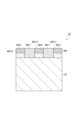
- FIG. 5 is a cross-sectional view of an example substrate to which the method of FIG. 4 may be applied.
- FIG. 6 is a cross-sectional view of another example substrate to which the method of FIG. 4 can be applied.
- FIG. 7 is a cross-sectional view of another example substrate to which the method of FIG. 4 can be applied.
- FIG. 5 is a cross-sectional view of an example substrate to which the method of FIG. 4 may be applied.
- FIG. 6 is a cross-sectional view of another example substrate to which the method of FIG. 4 can be applied.
- FIG. 7 is a cross-sectional view of another example substrate to which
- FIG. 8 is a cross-sectional view illustrating a step of a dry development method according to an exemplary embodiment.
- FIG. 9 is a cross-sectional view illustrating a step of a dry development method according to an exemplary embodiment.
- FIG. 10 is a cross-sectional view illustrating a step of a dry development method according to an exemplary embodiment.
- FIG. 11 is a schematic diagram of a dry development apparatus according to another exemplary embodiment.
- FIG. 12 is a schematic diagram of a dry development apparatus according to another exemplary embodiment.
- FIG. 13 is a schematic diagram of a substrate support according to another exemplary embodiment.
- FIG. 14 is a flow chart of a dry development method according to another exemplary embodiment.
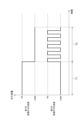
- FIG. 15 is a diagram illustrating an example of control of the flow rates of the first process gas and the second process gas.
- FIG. 16 is a diagram showing another example of control of the flow rates of the first process gas and the second process gas.
- FIG. 17 is a flowchart of a dry development method according to another exemplary embodiment.
- FIG. 18 is a schematic diagram of a substrate processing system according to an exemplary embodiment.
- FIG. 19 is a flow chart of a substrate processing method according to one exemplary embodiment.
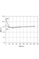
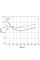
- FIG. 20 is a graph showing an example of the results of the first experiment.
- FIG. 21 is a graph showing an example of the results of the second experiment.
- FIG. 22 is a graph showing an example of the results of the third experiment.
- FIG. 23 is a table showing an example of the results of the fourth experiment.
- FIG. 1 is a schematic diagram of a dry development apparatus according to one exemplary embodiment.
- the heat treatment system includes a heat treatment apparatus 100 and a control unit 200.
- the heat treatment system is an example of a dry development system.
- the heat treatment apparatus 100 is an example of a dry development apparatus.
- the heat treatment apparatus 100 has a processing chamber 102 (chamber) that is configured to be airtight.
- the processing chamber 102 is, for example, an airtight cylindrical container, and is configured to be able to control the atmosphere inside.
- a side wall heater 104 is provided on the side wall of the processing chamber 102.
- a ceiling heater 130 is provided on the ceiling wall (top plate) of the processing chamber 102.
- a ceiling surface 140 of the ceiling wall (top plate) of the processing chamber 102 is formed, for example, as a horizontal flat surface. The temperature of the ceiling surface 140 is controlled by the ceiling heater 130.
- a substrate support 121 is provided at the lower side of the processing chamber 102.
- the substrate support 121 constitutes a mounting portion on which the substrate W is mounted.
- the substrate support 121 may have, for example, a circular surface (upper surface) or a horizontally formed surface (upper surface).
- the substrate W is mounted on the surface of the substrate support 121.
- a stage heater 120 is embedded in the substrate support 121. This stage heater 120 can heat the substrate W mounted on the substrate support 121.
- a ring assembly 125 may be disposed in the substrate support 121 so as to surround the substrate W.
- the ring assembly 125 may include one or more annular members. By disposing the ring assembly 125, the temperature controllability of the outer peripheral region of the substrate W can be improved.
- the ring assembly 125 may be made of an inorganic material or an organic material depending on the intended heat treatment.
- the substrate support 121 is supported in the processing chamber 102 by pillars 122 provided on the bottom surface of the processing chamber 102.
- a number of lift pins 123 that, for example, rise and fall vertically are provided on the circumferential outer side of the pillars 122.
- the lift pins 123 are inserted into a number of through holes provided at intervals in the circumferential direction of the substrate support 121.
- the lifting and lowering operation of the lift pins 123 is controlled by a lifting mechanism 124.
- the side wall of the processing chamber 102 is provided with an exhaust port 131 having an opening.
- the exhaust port 131 is connected to an exhaust mechanism 132 via an exhaust pipe.
- the exhaust mechanism 132 is composed of a vacuum pump, a valve, etc., and adjusts the exhaust flow rate from the exhaust port 131.
- the pressure inside the processing chamber 102 is adjusted by adjusting the exhaust flow rate, etc., using the exhaust mechanism 132.
- a transfer port for a substrate W (not shown) that can be opened and closed is formed in a position different from the position of the exhaust port 131 in the side wall of the processing chamber 102.
- a gas nozzle 141 is provided on the sidewall of the processing chamber 102 at a position different from the exhaust port 131 and the transfer port for the substrate W.
- the gas nozzle 141 supplies processing gas into the processing chamber 102.
- the gas nozzle 141 is provided on the sidewall of the processing chamber 102 on the opposite side of the exhaust port 131 when viewed from the center of the substrate support part 121.
- the gas nozzle 141 is formed in a rod shape that protrudes from the sidewall of the processing chamber 102 toward the center of the processing chamber 102.
- the tip of the gas nozzle 141 extends, for example horizontally, from the sidewall of the processing chamber 102.
- the processing gas is discharged into the processing chamber 102 from an outlet provided at the tip of the gas nozzle 141.
- the discharged processing gas flows in the direction of the arrow AR1 shown in FIG. 1 and is exhausted from the exhaust port 131.
- the tip of the gas nozzle 141 may extend diagonally downward toward the substrate W, or may extend diagonally upward toward the ceiling surface 140 of the processing chamber 102.
- the gas nozzle 141 may be provided, for example, in the ceiling wall of the processing chamber 102.
- the exhaust port 131 may be provided in the bottom surface of the processing chamber 102.
- the heat treatment apparatus 100 has a gas supply pipe 152 that is connected to a gas nozzle 141 from the outside of the processing chamber 102.
- a piping heater 160 for heating the inside of the gas supply pipe 152 is provided around the gas supply pipe 152.
- the gas supply pipe 152 is connected to a gas supply unit 170.
- the gas supply unit 170 includes at least one gas source and at least one flow rate controller.
- the gas supply unit may include a vaporizer that vaporizes the gas source in a liquid state.
- the control unit 200 processes computer-executable instructions that cause the heat treatment device 100 to perform the various steps described in this disclosure.
- the control unit 200 may be configured to control each element of the heat treatment device 100 to perform the various steps described herein. In one embodiment, a part or all of the control unit 200 may be included in the heat treatment device 100.
- the control unit 200 may include a processing unit 200a1, a storage unit 200a2, and a communication interface 200a3.
- the control unit 200 is realized, for example, by a computer 200a.
- the processing unit 200a1 may be configured to perform various control operations by reading a program from the storage unit 200a2 and executing the read program. This program may be stored in the storage unit 200a2 in advance, or may be acquired via a medium when necessary.
- the acquired program is stored in the storage unit 200a2 and is read from the storage unit 200a2 by the processing unit 200a1 and executed.
- the medium may be various storage media readable by the computer 200a, or may be a communication line connected to the communication interface 200a3.
- the processing unit 200a1 may be a CPU (Central Processing Unit).
- the storage unit 200a2 may include a RAM (Random Access Memory), a ROM (Read Only Memory), a HDD (Hard Disk Drive), a SSD (Solid State Drive), or a combination thereof.
- the communication interface 200a3 may communicate with the heat treatment device 100 via a communication line such as a LAN (Local Area Network).
- FIG. 2 is a schematic diagram of a dry developing apparatus according to another exemplary embodiment.
- the plasma processing system includes a plasma processing apparatus 1 and a control unit 2.
- the plasma processing system is an example of a dry developing system
- the plasma processing apparatus 1 is an example of a dry developing apparatus.
- the plasma processing apparatus 1 includes a plasma processing chamber (hereinafter also simply referred to as a "processing chamber") 10, a substrate support unit 11, and a plasma generation unit 12.
- the plasma processing chamber 10 has a plasma processing space.
- the plasma processing chamber 10 also has at least one gas supply port for supplying at least one processing gas to the plasma processing space, and at least one gas exhaust port for exhausting gas from the plasma processing space.
- the gas supply port is connected to a gas supply unit 20 described later, and the gas exhaust port is connected to an exhaust system 40 described later.
- the substrate support unit 11 is disposed in the plasma processing space and has a substrate support surface for supporting a substrate W.
- the plasma generating unit 12 is configured to generate plasma from at least one processing gas supplied into the plasma processing space.
- the plasma formed in the plasma processing space may be capacitively coupled plasma (CCP), inductively coupled plasma (ICP), electron-cyclotron-resonance plasma (ECR plasma), helicon wave plasma (HWP), or surface wave plasma (SWP), etc.
- various types of plasma generating units may be used, including an alternating current (AC) plasma generating unit and a direct current (DC) plasma generating unit.
- the AC signal (AC power) used in the AC plasma generation unit has a frequency in the range of 100 kHz to 10 GHz.
- the AC signal includes an RF (Radio Frequency) signal and a microwave signal.
- the RF signal has a frequency in the range of 100 kHz to 150 MHz.
- the control unit 2 processes computer-executable instructions that cause the plasma processing apparatus 1 to perform the various steps described in this disclosure.
- the control unit 2 may be configured to control each element of the plasma processing apparatus 1 to perform the various steps described herein. In one embodiment, a part or all of the control unit 2 may be included in the plasma processing apparatus 1.
- the control unit 2 is realized by, for example, a computer 2a.
- the control unit 2 may include a processing unit 2a1, a memory unit 2a2, and a communication interface 2a3. Each component of the control unit 2 may be the same as each component of the control unit 200 (see FIG. 1) described above.
- FIG. 3 is a schematic diagram of a dry development device according to another exemplary embodiment.
- the capacitively coupled plasma processing apparatus 1 includes a plasma processing chamber 10, a gas supply unit 20, a power supply 30, and an exhaust system 40.
- the plasma processing apparatus 1 also includes a substrate support unit 11 and a gas inlet unit.
- the gas inlet unit is configured to introduce at least one processing gas into the plasma processing chamber 10.
- the gas inlet unit includes a shower head 13.
- the substrate support unit 11 is disposed in the plasma processing chamber 10.
- the shower head 13 is disposed above the substrate support unit 11. In one embodiment, the shower head 13 constitutes at least a part of the ceiling of the plasma processing chamber 10.
- the plasma processing chamber 10 has a plasma processing space 10s defined by the shower head 13, the sidewall 10a of the plasma processing chamber 10, and the substrate support unit 11.
- the plasma processing chamber 10 is grounded.
- the shower head 13 and the substrate support unit 11 are electrically insulated from the housing of the plasma processing chamber 10.
- the substrate support 11 includes a main body 111 and a ring assembly 112.
- the main body 111 has a central region 111a for supporting the substrate W and an annular region 111b for supporting the ring assembly 112.
- a wafer is an example of a substrate W.
- the annular region 111b of the main body 111 surrounds the central region 111a of the main body 111 in a plan view.
- the substrate W is disposed on the central region 111a of the main body 111
- the ring assembly 112 is disposed on the annular region 111b of the main body 111 so as to surround the substrate W on the central region 111a of the main body 111. Therefore, the central region 111a is also called a substrate support surface for supporting the substrate W, and the annular region 111b is also called a ring support surface for supporting the ring assembly 112.
- the main body 111 includes a base 1110 and an electrostatic chuck 1111.
- the base 1110 includes a conductive member.
- the conductive member of the base 1110 may function as a lower electrode.
- the electrostatic chuck 1111 is disposed on the base 1110.
- the electrostatic chuck 1111 includes a ceramic member 1111a and an electrostatic electrode 1111b disposed within the ceramic member 1111a.
- the ceramic member 1111a has a central region 111a. In one embodiment, the ceramic member 1111a also has an annular region 111b. Note that other members surrounding the electrostatic chuck 1111, such as an annular electrostatic chuck or an annular insulating member, may have the annular region 111b.
- the ring assembly 112 may be disposed on the annular electrostatic chuck or the annular insulating member, or may be disposed on both the electrostatic chuck 1111 and the annular insulating member.
- At least one RF/DC electrode coupled to an RF power source 31 and/or a DC power source 32, which will be described later, may be disposed within the ceramic member 1111a.
- the at least one RF/DC electrode functions as a lower electrode.
- the RF/DC electrode is also called a bias electrode.
- the conductive member of the base 1110 and the at least one RF/DC electrode may function as multiple lower electrodes.
- the electrostatic electrode 1111b may function as a lower electrode.
- the substrate support 11 includes at least one lower electrode.
- the ring assembly 112 includes one or more annular members.
- the one or more annular members include one or more edge rings and at least one cover ring.
- the edge rings are formed of a conductive or insulating material, and the cover rings are formed of an insulating material.
- the substrate support 11 may include a temperature adjustment module configured to adjust at least one of the electrostatic chuck 1111, the ring assembly 112, and the substrate to a target temperature.
- the temperature adjustment module may include a heater, a heat transfer medium, a flow passage 1110a, or a combination thereof.
- a heat transfer fluid such as brine or a gas flows through the flow passage 1110a.
- the flow passage 1110a is formed in the base 1110, and one or more heaters are disposed in the ceramic member 1111a of the electrostatic chuck 1111.
- the substrate support 11 may also include a heat transfer gas supply configured to supply a heat transfer gas to a gap between the back surface of the substrate W and the central region 111a.
- the shower head 13 is configured to introduce at least one processing gas from the gas supply unit 20 into the plasma processing space 10s.
- the shower head 13 has at least one gas supply port 13a, at least one gas diffusion chamber 13b, and multiple gas inlets 13c.
- the processing gas supplied to the gas supply port 13a passes through the gas diffusion chamber 13b and is introduced into the plasma processing space 10s from the multiple gas inlets 13c.
- the shower head 13 also includes at least one upper electrode.
- the gas introduction unit may include, in addition to the shower head 13, one or more side gas injectors (SGI) attached to one or more openings formed in the side wall 10a.
- SGI side gas injectors
- the gas supply unit 20 may include at least one gas source 21 and at least one flow controller 22.
- the gas supply unit 20 is configured to supply at least one process gas from a respective gas source 21 through a respective flow controller 22 to the showerhead 13.
- Each flow controller 22 may include, for example, a mass flow controller or a pressure-controlled flow controller.
- the gas supply unit 20 may include at least one flow modulation device that modulates or pulses the flow rate of the at least one process gas.
- the power supply 30 includes an RF power supply 31 coupled to the plasma processing chamber 10 via at least one impedance matching circuit.
- the RF power supply 31 is configured to supply at least one RF signal (RF power) to at least one lower electrode and/or at least one upper electrode. This causes a plasma to be formed from at least one processing gas supplied to the plasma processing space 10s.
- the RF power supply 31 can function as at least a part of the plasma generating unit 12.
- a bias RF signal to at least one lower electrode, a bias potential is generated on the substrate W, and ion components in the formed plasma can be attracted to the substrate W.
- the RF power supply 31 includes a first RF generating unit 31a and a second RF generating unit 31b.
- the first RF generating unit 31a is coupled to at least one lower electrode and/or at least one upper electrode via at least one impedance matching circuit and configured to generate a source RF signal (source RF power) for plasma generation.
- the source RF signal has a frequency in the range of 10 MHz to 150 MHz.
- the first RF generating unit 31a may be configured to generate multiple source RF signals having different frequencies. The generated one or more source RF signals are supplied to at least one lower electrode and/or at least one upper electrode.
- the second RF generator 31b is coupled to at least one lower electrode via at least one impedance matching circuit and configured to generate a bias RF signal (bias RF power).
- the frequency of the bias RF signal may be the same as or different from the frequency of the source RF signal.
- the bias RF signal has a frequency lower than the frequency of the source RF signal.
- the bias RF signal has a frequency in the range of 100 kHz to 60 MHz.
- the second RF generator 31b may be configured to generate multiple bias RF signals having different frequencies.
- the generated one or more bias RF signals are provided to at least one lower electrode. Also, in various embodiments, at least one of the source RF signal and the bias RF signal may be pulsed.
- the power supply 30 may include a DC power supply 32 coupled to the plasma processing chamber 10.
- the DC power supply 32 includes a first DC generator 32a and a second DC generator 32b.
- the first DC generator 32a is connected to at least one lower electrode and configured to generate a first DC signal.
- the generated first DC signal is applied to the at least one lower electrode.
- the second DC generator 32b is connected to at least one upper electrode and configured to generate a second DC signal.
- the generated second DC signal is applied to the at least one upper electrode.
- the first and second DC signals may be pulsed.
- a sequence of voltage pulses is applied to at least one lower electrode and/or at least one upper electrode.
- the voltage pulses may have a rectangular, trapezoidal, triangular or combination thereof pulse waveform.
- a waveform generator for generating a sequence of voltage pulses from the DC signal is connected between the first DC generator 32a and at least one lower electrode.
- the first DC generator 32a and the waveform generator constitute a voltage pulse generator.
- the second DC generator 32b and the waveform generator constitute a voltage pulse generator
- the voltage pulse generator is connected to at least one upper electrode.
- the voltage pulses may have a positive polarity or a negative polarity.
- the sequence of voltage pulses may also include one or more positive polarity voltage pulses and one or more negative polarity voltage pulses within one period.
- the first and second DC generating units 32a and 32b may be provided in addition to the RF power source 31, or the first DC generating unit 32a may be provided in place of the second RF generating unit 31b.
- the exhaust system 40 may be connected to, for example, a gas exhaust port 10e provided at the bottom of the plasma processing chamber 10.
- the exhaust system 40 may include a pressure regulating valve and a vacuum pump. The pressure in the plasma processing space 10s is adjusted by the pressure regulating valve.
- the vacuum pump may include a turbomolecular pump, a dry pump, or a combination thereof.
- FIG. 4 is a flow chart of a dry development method (hereinafter, referred to as "method MT1") according to one exemplary embodiment.
- the method MT1 includes a step ST11 of providing a substrate W, a step ST12 of supplying a first processing gas, and a step ST13 of supplying a second processing gas.
- the method MT1 may include a step ST14 of determining whether or not a stop condition is satisfied after the step ST13.
- the method MT1 may include a step ST15 of purging the internal space of the chamber 102 between the steps ST12 and ST13.
- the method MT1 may include a step ST16 of purging the internal space of the chamber 102 between the steps ST13 and ST14. At least one of the steps ST15 and ST16 may be performed.
- the method MT1 may not include the steps ST15 and ST16.
- Method MT1 may be performed using any one of the substrate processing systems described above (see Figures 1 to 3), or may be performed using two or more of these substrate processing systems.
- method MT1 may be performed by a heat treatment system (see Figure 1).
- the control unit 200 controls each part of the heat treatment apparatus 100 to perform method MT1 on a substrate W.
- Step ST11 Providing a substrate
- the substrate W is provided in the processing chamber 102 of the thermal processing apparatus 100.
- the substrate W is provided on the substrate support 121, for example, by lowering the lift pins 123.
- the temperature of the substrate support 121 is adjusted to a set temperature.
- the temperature adjustment of the substrate support 121 may be performed by controlling the output of one or more of the sidewall heater 104, the stage heater 120, the ceiling heater 130, and the piping heater 160.
- the temperature of the substrate support 121 may be adjusted to a set temperature before step ST11. That is, the substrate W may be provided on the substrate support 121 after the temperature of the substrate support 121 is adjusted to the set temperature.
- FIG. 5 is a cross-sectional view of an example substrate W to which method MT1 can be applied.
- the substrate W includes an undercoat film UF and a metal-containing resist MF formed on the undercoat film UF.
- the substrate W may be used in the manufacture of semiconductor devices.
- the semiconductor devices include, for example, memory devices such as DRAMs and 3D-NAND flash memories, and logic devices.
- the metal-containing resist MF may contain at least one selected from the group consisting of tin (Sn), hafnium (Hf) and titanium (Ti).
- the metal-containing resist MF may contain, for example, at least one selected from the group consisting of tin oxide, hafnium oxide and titanium oxide, or may contain an organic substance.
- the metal-containing resist MF may be an EUV resist. As shown in FIG. 5, the metal-containing resist MF has an exposed first region MF1 and an unexposed second region MF2. The first region MF1 may be an exposed region exposed by EUV. The second region MF2 may be an unexposed region not exposed by EUV.
- the undercoat film UF may be formed on a silicon wafer.
- the undercoat film UF may be a carbon-containing film, a dielectric film, a metal film, a semiconductor film, or a laminated film thereof.
- FIGS. 6 and 7 are cross-sectional views of another example of a substrate W to which method MT1 can be applied.
- the base film UF may be composed of a first film UF1, a second film UF2, and a third film UF3.
- the base film UF may be composed of a second film UF2 and a third film UF3.
- the first film UF1 is, for example, a spin-on-glass (SOG) film, a SiC film, a SiON film, a Si-containing antireflective film (SiARC), or a carbon-containing film.
- the second film UF2 is, for example, a spin-on-carbon (SOC) film, an amorphous carbon film, or a silicon-containing film.
- the third film UF3 is, for example, a silicon-containing film.
- the silicon-containing film is, for example, a silicon oxide film, a silicon nitride film, a silicon oxynitride film, a silicon carbonitride film, a polycrystalline silicon film, or a carbon-containing silicon film.
- the third film UF3 may be formed by stacking a plurality of types of silicon-containing films.
- the third film UF3 may be formed by alternately stacking a silicon oxide film and a silicon nitride film.
- the third film UF3 may be formed by alternately stacking a silicon oxide film and a polycrystalline silicon film.
- the third film UF3 may be a stacked film including a silicon nitride film, a silicon oxide film, and a polycrystalline silicon film.
- the third film UF3 may be formed by stacking a silicon oxide film and a silicon carbonitride film.
- the third film UF3 may be a laminated film including a silicon oxide film, a silicon nitride film, and a silicon carbonitride film.
- the substrate W is formed as follows. First, a metal-containing photoresist film is formed on an undercoat film that has been subjected to adhesion treatment or the like.
- the film may be formed by a dry process, a wet process such as a solution coating method, or both a dry process and a wet process.
- a surface modification process of the undercoat film may be performed.
- the wafer after the film formation is heated, i.e., pre-baked (Post Apply Bake: PAB). An additional heating process may be performed after the pre-baking.
- the wafer after the heating process is transported to an exposure device, and the photoresist film is irradiated with EUV through an exposure mask (reticle).
- the first region MF1 is a region corresponding to an opening provided in the exposure mask (reticle).
- the second region MF2 is a region corresponding to a pattern provided in the exposure mask (reticle).
- EUV has a wavelength in the range of, for example, 10 nm to 20 nm. EUV may have a wavelength in the range of 11 nm to 14 nm, and in one example has a wavelength of 13.5 nm.
- the exposed wafer is transferred from the exposure tool to a thermal processing tool under atmospheric control and is subjected to a heat treatment, i.e., a post-exposure bake (PEB). The exposed wafer may be further heat-treated after the PEB.
- PEB post-exposure bake
- FIGS. 8 to 10 are cross-sectional views showing a step of a dry development method according to an exemplary embodiment.
- FIG. 8 is a cross-sectional view of the substrate W in step ST12.
- a first processing gas containing a fluorine-containing gas is supplied into the processing chamber 10, thereby forming a metal fluoride layer MF21 on the surface of the second region MF2 as shown in FIG. 8.
- step ST12 the fluorine contained in the fluorine-containing gas reacts with a metal (e.g., tin) present on the surface of the second region MF2 to form a metal fluoride layer MF21 (e.g., a tin fluoride (SnF) layer).
- a metal e.g., tin
- the metal fluoride layer MF21 may be formed without generating plasma.
- the supply of the first processing gas may be stopped.
- the fluorine-containing gas may include at least one selected from the group consisting of hydrogen fluoride gas (HF gas) and xenon fluoride gas (e.g., XeF2 gas).
- the first process gas may include an inert gas.
- the inert gas may include a noble gas.
- the inert gas may include at least one selected from the group consisting of nitrogen gas ( N2 gas), argon gas (Ar gas), xenon gas (Xe gas), and krypton gas (Kr gas).
- the partial pressure of the fluorine-containing gas supplied into the processing chamber 10 may be controlled.
- the partial pressure of the fluorine-containing gas may be 13.3 Pa or more.
- the partial pressure of the fluorine-containing gas may be 13.3 kPa or less.
- the partial pressure of the fluorine-containing gas may be 13.3 Pa or more and 13.3 kPa or less.
- the partial pressure of the fluorine-containing gas may be 0.1 Torr or more.
- the partial pressure of the fluorine-containing gas may be 100 Torr or less.
- the partial pressure of the fluorine-containing gas may be 0.1 Torr or more and 100 Torr or less.
- the substrate support 121 may be heated.
- Step ST12 may be performed in a state in which the temperature of the substrate support 121 is set to a first temperature.
- the first temperature may be 0° C. or higher.
- the first temperature may be 30° C. or higher.
- the first temperature may be 100° C. or higher.
- the first temperature may be 300° C. or lower.
- the first temperature may be 30° C. or higher and 300° C. or lower.
- Step ST15 Purge
- an inert gas may be supplied into the chamber 102, and gas or the like may be exhausted from within the chamber 102.
- the inert gas may include at least one selected from the group consisting of nitrogen gas and argon gas.
- Step ST13 Supply of second processing gas 9 is a cross-sectional view of the substrate W in step ST13.
- a second processing gas containing a chlorine-containing gas is supplied into the processing chamber 10 to remove the metal fluoride layer MF21 as shown in FIG. 9.
- the metal fluoride layer MF21 can be selectively removed from the first region MF1 by a reaction between the chlorine-containing gas and the metal fluoride layer MF21.
- a volatile metal chloride can be generated by an exchange reaction between the chlorine in the chlorine-containing gas and the fluorine in the metal fluoride layer MF21.
- a recess RE can be formed in the substrate W as shown in FIG.
- the supply of the second processing gas can be stopped.
- the chlorine-containing gas may include at least one selected from the group consisting of silicon tetrachloride gas ( SiCl4 gas), titanium tetrachloride gas ( TiCl4 gas), dimethylaluminum chloride gas (DMAC gas), thionyl chloride gas ( SOCl2 gas), and acetyl chloride gas ( CH3COCl gas).
- the second process gas may include an inert gas.
- the inert gas may include a noble gas.
- the inert gas may include at least one selected from the group consisting of nitrogen gas ( N2 gas), argon gas (Ar gas), xenon gas (Xe gas), and krypton gas (Kr gas).
- the pressure in the processing chamber 10 in step ST13 may be lower than the pressure in the processing chamber in step ST12.
- the partial pressure of the chlorine-containing gas supplied into the processing chamber 10 may be controlled.
- the partial pressure of the chlorine-containing gas may be 13.3 Pa or more.
- the partial pressure of the chlorine-containing gas may be 13.3 kPa or less.
- the partial pressure of the chlorine-containing gas may be 13.3 Pa or more and 13.3 kPa or less.
- the partial pressure of the chlorine-containing gas may be 0.1 Torr or more.
- the partial pressure of the fluorine-containing gas may be 100 Torr or less.
- the partial pressure of the chlorine-containing gas may be 0.1 Torr or more and 100 Torr or less.
- the substrate support 121 may be heated.
- Step ST13 may be performed in a state in which the temperature of the substrate support 121 is set to a second temperature.
- the second temperature may be the same as the first temperature, or may be higher than the first temperature.
- the second temperature may be 30°C or higher, or 100°C or higher.
- the second temperature may be 300°C or lower, or 200°C or lower.
- the second temperature may be 30°C or higher and 300°C or lower.
- Step ST16 Purge
- an inert gas may be supplied into the chamber 102, and gas or the like may be exhausted from within the chamber 102.
- the inert gas may include at least one selected from the group consisting of nitrogen gas and argon gas.
- Step ST12 and step ST13 may be repeated in this order. That is, method MT1 may include a step of repeating step ST12 and step ST13 (corresponding to step ST14). In the step of repeating step ST12 and step ST13, at least one of step ST15 and step ST16 may be repeated. The step of repeating step ST12 and step ST13 may be repeated a predetermined number of times. The step of repeating step ST12 and step ST13 may be repeated until the recess RE reaches the base film UF (until the base film UF is exposed). The step of performing step ST12 and step ST13 once each may be considered as one cycle. In this case, the thickness of the second region MF2 removed per cycle in the direction from the metal-containing resist MF toward the base film UF may be 5 nm or more and 20 nm or less.
- the process of repeating process ST12 and process ST13 may include changing at least one selected from the group consisting of the pressure in the chamber 102, the temperature of the substrate support part 121, the processing time of process ST12, and the processing time of process ST13, depending on the aspect ratio of the recess RE formed in process ST13.
- the process of repeating process ST12 and process ST13 may include performing at least one of lowering the pressure in the chamber 102, lowering the temperature of the substrate support part 121, shortening the processing time of process ST12, and shortening the processing time of process ST13, depending on an increase in the aspect ratio of the recess RE formed in process ST13.
- each parameter may be adjusted according to the aspect ratio of recessed portion RE each time steps ST12 and ST13 are repeated.
- Each parameter may be adjusted based on the absolute value of the aspect ratio, or based on the increase in the aspect ratio. For example, in method MT1, each parameter may be decreased by several percent to several tens of percent according to the increase in the aspect ratio of recessed portion RE each time steps ST12 and ST13 are repeated. A limit may be set on the number of times each parameter is adjusted.
- a table showing the relationship between the aspect ratio of the recess RE and each parameter may be stored in the memory unit 200a2 of the control unit 200.
- the control unit 200 may adjust each parameter based on the table stored in the memory unit 200a2.
- the method MT1 may include a step ST14 for determining whether or not a stop condition is satisfied.
- the stop condition may be satisfied when the removal amount (depth of the recess RE) of the second region MF2 reaches a threshold value.
- the stop condition may be satisfied when the undercoat film UF is exposed.
- the stop condition may be satisfied when the total processing time of the steps ST12 and ST13 reaches a threshold value.
- the stop condition may be satisfied when the number of repetitions of the steps ST12 and ST13 reaches a threshold value.
- the steps ST12 and ST13 may be repeated again.
- the processing conditions may be changed from the previous cycle to perform the next cycle.
- the partial pressure of the fluorine-containing gas and the partial pressure of the chlorine-containing gas may be changed.
- the temperature of the substrate support 121 may be changed, or the type of noble gas may be changed.
- the above-mentioned changes may be appropriately combined.
- the stop condition is satisfied in step ST14 (step ST14: YES)
- the method MT1 may end.
- the second region MF2 can be selectively removed relative to the first region MF1.
- the metal-containing resist can be appropriately developed.
- the first region MF1 can be removed at a first rate, while the second region MF2 can be removed at a second rate that is higher than the first rate.
- the first rate is, for example, 1 nm/cycle or less.
- the second rate is, for example, 2 nm/cycle or more and 10 nm/cycle or less.
- the second region MF2 can be removed with a high selectivity ratio (the ratio of the rate at which the second region MF2 is removed to the rate at which the first region MF1 is removed) relative to the first region MF1.
- both the first region MF1 and the second region MF2 contain bonds between tin and oxygen (Sn-O bonds).
- Sn-O bonds bonds between tin and oxygen
- the first region MF1 contains a greater number of Sn-O bonds than the second region MF2. In other words, the density of Sn-O bonds per unit volume is relatively high in the first region MF1.
- the replacement of Sn-F bonds by the fluorine-containing gas is more likely to occur to a deeper position in the second region MF2 than in the first region MF1. Furthermore, the number of organic ligands contained in the second region MF2 is greater than the number of organic ligands contained in the first region MF1. Therefore, the second region MF2 is more likely to volatilize than the first region MF1.
- the thickness of the metal fluoride layer MF21 formed in step ST12 saturates at a certain point. Therefore, the depth of the recess RE formed in step ST13 (the amount of the second region MF2 removed) can be controlled. Therefore, according to method MT1, high in-plane uniformity can be obtained for the depth of the recess RE. In other words, the difference between the depth of the recess RE at the center of the substrate W and the depth of the recess RE at the periphery of the substrate W can be reduced.
- step ST12 damage to the substrate W or the substrate support part 121 can be suppressed compared to when plasma is used.
- process ST12 if the first temperature of the substrate support portion 121 is 30°C or higher, the reaction between the second region MF2 and the fluorine-containing gas is promoted.
- the second temperature of the substrate support part 121 in step ST13 may be higher than the first temperature of the substrate support part 121 in step ST12.
- the reaction between the metal fluoride layer MF21 and the chlorine-containing gas is promoted, and therefore the removal of the metal fluoride layer MF21 is also promoted.
- the metal fluoride layer MF21 is a SnF layer
- the reaction between the chlorine-containing gas and SnF may exchange F in SnF for Cl.
- highly volatile SnCl may be generated.
- method MT1 includes repeating steps ST12 and ST13, the thickness of the second region MF2 that is removed in the direction from the metal-containing resist MF toward the undercoat film UF can be increased.
- the process of repeating step ST12 and step ST13 may include performing at least one of the following in response to an increase in the aspect ratio of the recessed portion RE formed in step ST13: lowering the pressure in the chamber 102, lowering the temperature of the substrate support portion 121, shortening the processing time of step ST12, and shortening the processing time of step ST13.
- the recessed portion RE of the metal-containing resist MF tends to have an inverted tapered shape that becomes wider toward the bottom (toward the undercoat film UF).
- the progress of dry development is suppressed, for example, by lowering the pressure in the chamber 102 in response to an increase in the aspect ratio of the recessed portion RE.
- the sidewall of the recessed portion RE is less likely to be scraped off, and the sidewall shape of the recessed portion RE after development can be made closer to vertical.
- FIGS. 11 and 12 are diagrams that show a schematic diagram of a dry developing apparatus according to another exemplary embodiment.
- FIG. 11 is a schematic cross-sectional view showing a configuration example of the heat treatment apparatus 100a.
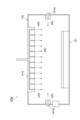
- FIG. 12 is a schematic plan view showing a configuration example of the heat treatment apparatus 100a.
- the heat treatment apparatus 100a includes a shower head 141a provided on the ceiling of the processing chamber 102 and a plurality of gas nozzles 141b provided on the side wall of the processing chamber 102.
- the shower head 141a may be disposed so as to face the substrate support 121.
- the plurality of gas nozzles 141b may be disposed, for example, on the side wall of the processing chamber 102 at equal intervals along the circumferential direction.
- the plurality of gas nozzles 141b may include a first gas nozzle 141b1 and a second gas nozzle 141b2.
- the first gas nozzle 141b1 and the second gas nozzle 141b2 may be arranged alternately.
- the types of gas supplied from the shower head 141a, the gas nozzle 141b1, and the gas nozzle 141b2 into the processing chamber 102 may be the same or different.
- the gas from the shower head 141a is supplied into the processing chamber 102 in the direction of the arrow AR2 shown in FIG. 11.
- the gas from the gas nozzle 141b1 is supplied into the processing chamber 102 in the direction of the arrow AR3 shown in FIG. 11 and FIG. 12.
- the gas from the gas nozzle 141b2 is supplied into the processing chamber 102 in the direction of the arrow AR4 shown in FIG. 11 and FIG. 12.
- the flow rates of the gas supplied from the shower head 141a, the gas nozzle 141b1, and the gas nozzle 141b2 into the processing chamber 102 may be the same or different.
- Heaters may be arranged on the sidewalls of the substrate support 121 and the processing chamber 102.
- a gas exhaust port may be located at the bottom of the processing chamber 102 .
- the heat treatment apparatus 100a makes it easy to control the gas density in the processing chamber 102, improving the in-plane uniformity in the development of the metal-containing resist MF.
- a substrate support 121a shown in FIG. 13 may be used instead of the substrate support 121 shown in FIG. 13 is a diagram showing a schematic view of a substrate support 121a according to another exemplary embodiment.
- the substrate support 121a shown in FIG. 13 has a plurality of zones, and each zone is provided with a heater electrode.
- the substrate support 121a has zones Z1 to Z14.
- the heater electrodes of the zones Z1 to Z14 are configured to be able to be supplied with power independently. That is, the substrate support 121a is configured to be able to control the temperature independently for each zone. Therefore, the substrate support 121a can improve the in-plane uniformity in the development of the metal-containing resist MF.
- the method MT1 may be performed by the plasma processing apparatus 1 shown in FIG. 2 and FIG. 3 instead of the heat treatment apparatus 100a.
- the metal fluoride layer MF21 may be generated by using plasma generated from a first processing gas containing a fluorine-containing gas.
- the fluorine-containing gas may include at least one selected from the group consisting of hydrogen fluoride gas (HF gas), xenon fluoride gas, fluorocarbon gas, hydrofluorocarbon gas, nitrogen fluoride gas, and sulfur fluoride gas.
- the fluorocarbon gas may include at least one selected from the group consisting of C 4 F 6 gas, C 4 F 8 gas, C 3 F 8 gas, and CF 4 gas.
- the hydrofluorocarbon gas may include at least one selected from the group consisting of CHF 3 gas and CH 2 F 2 gas.
- the nitrogen fluoride gas may include NF 3 gas.
- the sulfur fluoride gas may include SF6 gas.
- a precoat may be applied to the sidewall of the processing chamber 102 or parts in the processing chamber 102 such as the substrate support 121 (hereinafter also referred to as “chamber parts") before the start of development.
- the precoat may be performed by atomic layer deposition (hereinafter also referred to as "ALD method"), chemical vapor deposition (hereinafter also referred to as "CVD method”), or the like.
- a gas capable of forming a film having resistance to a processing gas containing a carboxylic acid may be selected as the gas for forming the precoat.
- a silicon-containing gas may be used as the gas for forming the precoat.
- the silicon-containing gas may include at least one selected from the group consisting of aminosilane and SiCl4 .
- a silicon oxide film may be formed as a precoat on the sidewall of the processing chamber 102 or the parts in the chamber. This makes it possible to suppress corrosion of the sidewall of the processing chamber 102 or the parts in the chamber caused by the processing gas.
- the sidewalls of the processing chamber 102 and the parts inside the chamber may be made of a material that is resistant to processing gases containing carboxylic acids, etc.
- the inside of the processing chamber 102 may be cleaned after development.
- the processing chamber 102 and the parts inside the chamber may be heated, and then a cleaning gas may be supplied into the processing chamber 102.
- a gas containing hydrogen halide may be used as the cleaning gas.
- the gas containing hydrogen halide may include at least one selected from the group consisting of hydrogen bromide gas (HBr gas) and hydrogen fluoride gas.
- the cleaning may be performed by a thermal atomic layer etching method (hereinafter also referred to as the "thermal ALE method"). This makes it possible to remove metal oxides that adhere to the sidewalls of the processing chamber 102 and the parts inside the chamber during development.
- the base film UF may be etched using the metal-containing resist MF developed by the method MT1 as a mask.
- the etching conditions for the base film UF may be selected based on the film type of the base film UF.
- the etching of the base film UF may be performed by the plasma processing apparatus 1 shown in FIG.
- [Seventh embodiment] 14 is a flowchart of a dry development method (hereinafter referred to as "method MT2") according to another exemplary embodiment.
- the method MT2 includes a step ST21 of providing a substrate W and a step ST22 of supplying a processing gas.
- the method MT2 may include a step ST23 of determining whether a stop condition is satisfied after the step ST22.
- the substrate W may be the same as the substrate W of the first embodiment.
- the method MT2 develops the metal-containing resist MF.
- a process gas containing a fluorine-containing gas and a chlorine-containing gas is supplied into the process chamber 102 to remove the second region MF2.
- a mixed gas containing a fluorine-containing gas and a chlorine-containing gas may be supplied as the process gas. That is, in step ST22, a fluorine-containing gas and a chlorine-containing gas may be supplied simultaneously.
- a step of forming a metal fluoride layer MF21 on the surface of the second region MF2 with a fluorine-containing gas and a step of removing the metal fluoride layer MF21 with a chlorine-containing gas may be performed simultaneously.
- the types of gases contained in the fluorine-containing gas and the chlorine-containing gas may be the same as those in method MT1.
- the ratio (F2/F1) of the flow rate F2 of the chlorine-containing gas to the flow rate F1 of the fluorine-containing gas may be adjusted as appropriate.
- F2/F1 may be changed during the performance of step ST22.
- F2/F1 may be changed as appropriate according to the processing time of step ST22 or according to the aspect ratio of the recess RE formed in step ST22. For example, as the aspect ratio of the recess RE increases, the flow rates of the fluorine-containing gas and the chlorine-containing gas may be adjusted so that F2/F1 increases, or the flow rates of the fluorine-containing gas and the chlorine-containing gas may be adjusted so that F2/F1 decreases.
- Process ST22 may include reducing the pressure in the chamber 102 in response to an increase in the aspect ratio of the recess RE.
- Process ST22 may include changing at least one selected from the group consisting of the pressure in the chamber 102, the temperature of the substrate support part 121, the processing time of process ST12, and the processing time of process ST13 in response to an increase in the aspect ratio of the recess RE.
- process ST22 may include performing at least one of reducing the pressure in the chamber 102, reducing the temperature of the substrate support part 121, shortening the processing time of process ST12, and shortening the processing time of process ST13 in response to an increase in the aspect ratio of the recess RE.
- Each parameter may be adjusted based on the absolute value of the aspect ratio, or based on the increase in the aspect ratio.
- the pressure in the chamber 102 may be reduced in response to the increase in the aspect ratio of the recess RE.
- Step ST22 may include a first period and a second period following the first period.
- F2/F1 in the first period may be larger or smaller than F2/F1 in the second period.
- step ST22 the temperature of the substrate support 121 can be controlled.
- An example of the temperature of the substrate support 121 in step ST22 may be the same as the example of the temperature of the substrate support 121 in step ST12 or step ST13 of method MT1.
- the method MT2 may have a step ST23 for determining whether or not a stop condition is satisfied.
- the step ST23 may be performed in the same manner as the step ST14 of the method MT1.
- the stop condition may be satisfied when the amount of removal of the second region MF2 (depth of the recess RE) reaches a threshold value.
- the stop condition may be satisfied when the base film UF is exposed.
- the stop condition may be satisfied when the processing time of the step ST22 reaches a threshold value.
- the step ST23 if the stop condition is not satisfied (step ST23: NO), the step ST22 may be repeated. In that case, in the method MT2, the processing conditions may be changed from the previous step ST22 to perform the next step ST22.
- step ST23 the partial pressure of the fluorine-containing gas and the partial pressure of the chlorine-containing gas may be changed.
- the temperature of the substrate support 121 may be changed, or the type of noble gas may be changed.
- the above-mentioned changes may be appropriately combined.
- Eighth embodiment 15 is a diagram showing an example of control of the flow rate of the first process gas and the flow rate of the second process gas in the method MT1.
- the step of repeating the steps ST12 and ST13 in the method MT1 may include a first period P1 in which the step ST12 is performed for a first processing time T1 and the step ST13 is performed for a second processing time T2.
- the step of repeating the steps ST12 and ST13 may include a second period P2 after the first period P1.
- the step ST12 is performed for a third processing time T3 that is shorter than the first processing time T1
- the step ST13 is performed for a fourth processing time T4 that is shorter than the second processing time T2.
- the flow rate of the first processing gas is at a high level, while the flow rate of the second processing gas is adjusted to a low level.
- process ST12 proceeds.
- the high level flow rate may be greater than the low level flow rate.
- the low level flow rate may be 50% or less of the high level flow rate, or may be 20% or less.
- the low level flow rate may be zero.
- the flow rate of the first processing gas is at a low level, while the flow rate of the second processing gas is adjusted to a high level. As a result, during the second processing time T2, process ST13 proceeds.
- the flow rate of the first processing gas is at a high level, while the flow rate of the second processing gas is adjusted to a low level.
- process ST12 proceeds.
- the flow rate of the first processing gas is adjusted to a low level, while the flow rate of the second processing gas is adjusted to a high level.
- step ST13 proceeds.
- the length of the third processing time T3 may be 80% or less, 50% or less, or 20% or less of the length of the first processing time T1.
- the length of the fourth processing time T4 may be 80% or less, 50% or less, or 20% or less of the length of the second processing time T2.
- the progress of dry development is suppressed as the aspect ratio of the recessed portion RE increases.
- the sidewall of the recessed portion RE is less likely to be scraped off, and the shape of the sidewall of the recessed portion RE after development can be made closer to vertical.
- the second period P2 is performed at the end of the dry development (when the bottom of the recessed portion RE reaches the base film UF during the second period P2), the removal selectivity of the second region MF2 relative to the base film UF can be improved.
- [Ninth embodiment] 16 is a diagram showing another example of the control of the flow rate of the first process gas and the flow rate of the second process gas in the method MT1.
- one of the first process gas and the second process gas may be continuously supplied into the chamber 102.
- the other of the first process gas and the second process gas may be supplied into the chamber 102 so that a Hi level flow rate (first gas flow rate) and a Low level flow rate (second gas flow rate) lower than the Hi level flow rate are alternated.
- the other of the first process gas and the second process gas may be intermittently supplied into the chamber 102.
- both the first process gas and the second process gas may be supplied into the chamber 102 so that a Hi level flow rate and a Low level flow rate are alternated.
- step ST12 proceeds during a first processing time T1
- step ST13 proceeds during a second processing time T2 following the first processing time T1.
- the low level flow rate may be 50% or less of the high level flow rate, or it may be 20% or less.
- the low level flow rate may be zero.
- the first processing gas is continuously supplied into the chamber 102 at a high level.
- the second processing gas is supplied into the chamber 102 so that the flow rate is alternately high and low. This is not limited to the above, and during the first processing time T1, the first processing gas may be supplied into the chamber 102 so that the flow rate is alternately high and low.
- the second processing gas may be continuously supplied into the chamber 102 at a high level.
- At least one of the first processing gas and the second processing gas may be pulse-controlled by the control unit 200 so that a high level flow rate and a low level flow rate are alternately supplied.
- the duty ratio of the pulse in the pulse control may be 50%.
- the duty ratio of the pulse in the pulse control may be 20% or more, or 70% or more.
- the method according to the ninth embodiment can reduce the amount of gas used compared to when both the first processing gas and the second processing gas are supplied continuously.
- FIG. 17 is a flow chart of a dry development method (hereinafter referred to as "method MT3") according to another exemplary embodiment.
- the method MT3 may be performed by the plasma processing apparatus 1 of FIG. 2 or FIG. 3.
- the method MT3 may have a step ST12A and a step ST12B instead of the step ST12 in the method MT1.
- the step ST12B may be performed after the step ST12A or before the step ST12A.
- the metal fluoride layer MF21 may be formed on the surface of the second region MF2 by supplying a first processing gas containing a fluorine-containing gas into the processing chamber 10 without generating plasma (see FIG. 8).
- the metal fluoride layer MF21 may be generated by using plasma generated from the first processing gas containing a fluorine-containing gas.
- active species such as fluorine ions and fluorine radicals can be generated.
- Example of the configuration of a substrate processing system 18 is a schematic diagram of a substrate processing system SS according to an example embodiment, which includes a first carrier station CS1, a first processing station PS1, a first interface station IS1, an exposure apparatus EX, a second interface station IS2, a second processing station PS2, a second carrier station CS2, and a controller CT.
- the first carrier station CS1 loads and unloads the first carrier C1 between the substrate processing system SS and an external system.
- the first carrier station CS1 has a loading stage on which multiple first loading plates ST1 are provided.
- the first carrier C1 is loaded on each of the first loading plates ST1.
- the first carrier C1 has a housing capable of accommodating multiple substrates W therein.
- the first carrier C1 is loaded on each of the first loading plates ST1 when it is accommodating multiple substrates W or when it is empty and does not accommodate any substrates W.
- the first carrier C1 is, in one example, a FOUP (Front Opening Unified Pod).
- the first carrier station CS1 transports the substrate W between the first carrier C1 and the first processing station PS1.
- the first carrier station CS1 is provided with a first transport device HD1 located between the mounting table and the first processing station PS1.
- the first processing station PS1 is provided with a second transport device HD2.
- the first transport device HD1 transports the substrate W between the first carrier C1 on each first mounting plate ST1 and the second transport device HD2 in the first processing station PS1.
- a load lock module may be provided between the first carrier station CS1 and the first processing station PS1.
- the load lock module can switch the pressure in the load lock module to atmospheric pressure or vacuum.
- "Atmospheric pressure" may be the pressure inside the first transport device HD1.
- “Vacuum” is a pressure lower than atmospheric pressure, and may be a medium vacuum of, for example, 0.1 Pa to 100 Pa.
- the inside of the second transport device HD2 may be atmospheric pressure or vacuum.
- the load lock module may, for example, transfer a substrate W from a first transfer device HD1 at atmospheric pressure to a second transfer device HD2 at vacuum.
- the load lock module may, for example, transfer a substrate W from a second transfer device HD2 at vacuum to a first transfer device HD1 at atmospheric pressure.
- the first processing station PS1 performs various processes on the substrate W.
- the first processing station PS1 includes a pre-processing module PM1, a resist film forming module PM2, and a first heat treatment module PM3 (hereinafter collectively referred to as the "first substrate processing module PMa").
- the second transport device HD2 in the first processing station PS1 transports the substrate W.
- the second transport device HD2 transports the substrate W between the first substrate processing modules PMa.
- the second transport device HD2 transports the substrate W between the first processing station PS1 and the first carrier station CS1, or between the first processing station PS1 and the first interface station IS1.
- the pre-treatment module PM1 performs pre-treatment on the substrate W.
- the pre-treatment module PM1 includes a temperature adjustment unit that adjusts the temperature of the substrate W, or a high-precision temperature adjustment unit that adjusts the temperature of the substrate W with high precision.
- the pre-treatment module PM1 includes a hydrophobization treatment unit that performs a surface modification treatment on the substrate W.
- Each treatment unit in the pre-treatment module PM1 may be configured to include a heat treatment device 100 (see FIG. 1) and a plasma treatment device 1 (see FIG. 2 and FIG. 3).
- the resist film forming module PM2 forms a resist film on the substrate W.
- the resist film forming module PM2 includes a dry coating unit.
- the dry coating unit forms a resist film on the substrate W using a dry process such as a vapor phase deposition method.
- the dry coating unit may include a CVD device or an ALD (Atomic Layer Deposition) device that chemically vapor deposits a resist film on the substrate W.
- the dry coating unit may include a PVD (Physical Vapor Deposition) device that physically vapor deposits a resist film.
- the dry coating unit may be a heat treatment device 100 (see FIG. 1) or a plasma treatment device 1 (see FIG. 2 and FIG. 3).
- the resist film forming module PM2 includes a wet coating unit.
- the wet coating unit forms a resist film on the substrate W using a wet process such as a solution coating method.
- the resist film forming module PM2 includes both a wet coating unit and a dry coating unit.
- the first thermal treatment module PM3 thermally treats the substrate W.
- the first thermal treatment module PM3 includes one or more of a pre-bake (PAB) unit that heat-treats the substrate W on which a resist film has been formed, a temperature adjustment unit that adjusts the temperature of the substrate W, and a high-precision temperature adjustment unit that adjusts the temperature of the substrate W with high precision.
- PAB pre-bake
- Each of these units may have one or more thermal treatment devices.
- the multiple thermal treatment devices may be configured by stacking the thermal treatment devices.
- the thermal treatment device may be, for example, the thermal treatment device 100 (see FIG. 1).
- the thermal treatment may be performed at a predetermined temperature using a predetermined gas.
- the first interface station IS1 has a third transport device HD3.
- the third transport device HD3 transports the substrate W between the first processing station PS1 and the exposure device EX.
- the third transport device HD3 has a housing that houses the substrate W.
- the third transport device HD3 may be configured to be able to control the temperature, humidity, pressure, etc. within the housing.
- the exposure apparatus EX exposes the resist film on the substrate W using an exposure mask (reticle).
- the exposure apparatus EX may be, for example, an EUV exposure apparatus that uses EUV as a light source.
- the second interface station IS2 has a fourth transport device HD4.
- the fourth transport device HD4 transports the substrate W between the exposure device EX and the second processing station PS2.
- the fourth transport device HD4 has a housing that houses the substrate W.
- the fourth transport device HD4 may be configured to be able to control the temperature, humidity, pressure, etc. within the housing.
- the second processing station PS2 performs various processes on the substrate W.
- the second processing station PS2 includes a second heat treatment module PM4, a measurement module PM5, a development module PM6, and a third heat treatment module PM7 (hereinafter collectively referred to as the "second substrate processing module PMb").
- the second processing station PS2 has a fifth transport device HD5.
- the fifth transport device HD5 transports the substrate W.
- the fifth transport device HD5 transports the substrate W between the second substrate processing modules PMb.
- the fifth transport device HD5 transports the substrate W between the second processing station PS2 and the second carrier station CS2, or between the second processing station PS2 and the second interface station IS2.
- the second thermal treatment module PM4 performs thermal treatment on the substrate W.
- the second thermal treatment module PM4 may include a post-exposure bake (PEB) unit that heat-treats the substrate W after exposure.
- the second thermal treatment module PM4 may include a temperature adjustment unit that adjusts the temperature of the substrate W.
- the second thermal treatment module PM4 may include a high-precision temperature adjustment unit that adjusts the temperature of the substrate W with high precision.
- the second thermal treatment module PM4 may include any one or more of these.
- Each of these units may have one or more thermal treatment devices.
- the multiple thermal treatment devices may be configured by stacking the thermal treatment devices.
- the thermal treatment device may be, for example, the thermal treatment device 100 (see FIG. 1).
- the thermal treatment may be performed at a predetermined temperature using a predetermined gas.
- the measurement module PM5 measures the substrate W.
- the measurement module PM5 includes an imaging unit including a stage for placing the substrate W, an imaging device, a lighting device, and various sensors (temperature sensor, reflectance measurement sensor, etc.).
- the imaging device may be, for example, a CCD camera that captures an image of the appearance of the substrate W, or a hyperspectral camera that captures images by dispersing light into wavelengths.
- the hyperspectral camera can measure one or more of the pattern shape, dimensions, film thickness, composition, and film density of the resist film.
- the developing module PM6 develops the substrate W.
- the developing module PM6 includes a dry developing unit that dry develops the substrate W.
- the dry developing unit may be, for example, the heat treatment device 100 (see FIG. 1) or the plasma treatment device 1 (see FIG. 2 and FIG. 3).
- the third heat treatment module PM7 heat treats the substrate W.
- the third heat treatment module PM7 may include a post bake (PB) unit that heat treats the substrate W after development.
- the third heat treatment module PM7 may include a temperature adjustment unit that adjusts the temperature of the substrate W.
- the third heat treatment module PM7 may include a high-precision temperature adjustment unit that adjusts the temperature of the substrate W with high precision.
- the third heat treatment module PM7 may include any one or more of these.
- Each of these units may have one or more heat treatment devices.
- the multiple heat treatment devices may be configured by stacking the heat treatment devices.
- the heat treatment device may be, for example, the heat treatment device 100 (see FIG. 1).
- the heat treatment may be performed at a predetermined temperature using a predetermined gas.
- the second carrier station CS2 transports the second carrier C2 between the substrate processing system SS and an external system.
- the configuration and functions of the second carrier station CS2 may be the same as those of the first carrier station CS1 described above.
- the control unit CT controls each component of the substrate processing system SS to perform the above-mentioned series of processes on the substrate W.
- the control unit CT stores a recipe in which the process procedure, process conditions, transport conditions, etc. are set.
- the control unit CT controls each component of the substrate processing system SS according to the recipe.
- the control unit CT may have some or all of the functions of each control unit (control unit 200, control unit 2, control unit 400) shown in Figures 1 to 4.
- FIG. 19 is a flowchart of a substrate processing method (hereinafter, referred to as "method MT4") according to one exemplary embodiment.
- method MT4 includes steps ST100 to ST900.
- Step ST100 is a step of performing a pretreatment on a substrate.
- Step ST200 is a step of forming a resist film on a substrate W.
- Step ST300 is a step of performing a heat treatment (pre-bake: PAB) on the substrate W on which the resist film has been formed.
- Step ST400 is a step of exposing the substrate W to EUV light.
- Step ST500 is a step of performing a heat treatment (post-exposure bake: PEB) on the substrate W after exposure.
- PEB post-exposure bake
- Step ST600 is a step of measuring the substrate W.
- Step ST700 is a step of developing the resist film on the substrate W.
- Step ST800 is a step of performing a heat treatment (post-bake: PB) on the substrate W after development.
- Step ST900 is a step of etching the substrate W.
- the method MT4 may not include one or more of the above steps. For example, the method MT4 may not include the step ST600, or the step ST700 may be performed after the step ST500.
- Method MT4 may be performed using the substrate processing system SS shown in FIG. 18.
- a control unit CT of the substrate processing system SS controls each part of the substrate processing system SS to perform method MT4 on a substrate W.
- Step ST100 Pretreatment
- a first carrier C1 accommodating a plurality of substrates W is loaded into a first carrier station CS1 of a substrate processing system SS.
- the first carrier C1 is placed on a first placement plate ST1.
- the first transport device HD1 sequentially takes out each substrate W from the first carrier C1 and transports it to a second transport device HD2 in a first processing station PS1.
- the substrate W is transported to a pre-processing module PM1 by the second transport device HD2.
- the substrate W is pre-processed by the pre-processing module PM1.
- the pre-processing may include, for example, one or more of temperature adjustment of the substrate W, formation of a part or all of an undercoat film on the substrate W, heating treatment of the substrate W, and high-precision temperature adjustment of the substrate W.
- the pre-processing may include a surface modification treatment of the substrate W.
- Step S200 Forming a resist film
- the substrate W is transported to the resist film forming module PM2 by the second transport device HD2.
- a resist film is formed on the substrate W by the resist film forming module PM2.
- the resist film is formed by a wet process such as a solution coating method.
- the resist film is formed by spin-coating the resist film on the substrate W using a wet coating unit of the resist film forming module PM2.
- the resist film is formed on the substrate W by a dry process such as a vapor phase deposition method.
- the resist film is formed by vapor-depositing the resist film on the substrate W using a dry coating unit of the resist film forming module PM2.
- the formation of a resist film on the substrate W may be performed using both a dry process and a wet process.
- a second resist film may be formed on the first resist film by a wet process.
- the film thickness, material, and composition of the first resist film may be the same as or different from the film thickness, material, and composition of the second resist film.
- Step ST300: PAB Next, the substrate W is transported to the first thermal treatment module PM3 by the second transport device HD2.
- the substrate W is subjected to a heat treatment (pre-baking: PAB) by the first thermal treatment module PM3.
- the pre-baking may be performed in an air atmosphere or in an inert atmosphere.
- the substrate W may be heated to 50° C. or more and 250° C. or less, 50° C. or more and 200° C. or less, or 80° C. or more and 150° C. or less.
- the pre-baking may be performed continuously by the dry coating unit that performed the process ST200.
- a process Edge Bead Removal: EBR
- EBR Err Bead Removal
- Step ST400 EUV exposure
- the substrate W is transferred by the second transport device HD2 to the third transport device HD3 in the first interface station IS1.
- the substrate W is then transported by the third transport device HD3 to the exposure apparatus EX.
- the substrate W is EUV exposed through an exposure mask (reticle) in the exposure apparatus EX.
- a first region that is EUV exposed and a second region that is not EUV exposed are formed on the substrate W in accordance with the pattern of the exposure mask (reticle).
- the substrate W is transferred from the fourth transfer device HD4 in the second interface station IS2 to the fifth transfer device HD5 in the second processing station PS2.
- the substrate W is then transferred by the fifth transfer device HD5 to the second thermal treatment module PM4, where it is subjected to a heat treatment (post-exposure bake: PEB).
- the post-exposure bake may be performed in an air atmosphere. In the post-exposure bake, the substrate W may be heated to 180° C. or more and 250° C. or less.
- Step ST600 Measurement
- the substrate W is transported to the measurement module PM5 by the fifth transport device HD5.
- the substrate W is measured by the measurement module PM5.
- the measurement may be optical measurement.
- the measurement by the measurement module PM5 includes measurement of the appearance and dimensions of the substrate W using a CCD camera.
- the measurement by the measurement module PM5 includes measurement of one or more of the pattern shape, dimensions, film thickness, composition, and film density of the resist film (hereinafter also referred to as "pattern shape, etc.”) using a hyperspectral camera.
- control unit CT determines whether or not there is an exposure abnormality in the substrate W based on the measured appearance, dimensions, pattern shape, etc. of the substrate W. In one embodiment, if the control unit CT determines that there is an exposure abnormality in the substrate W, the substrate W may be reworked or discarded without being developed by process ST700. Reworking of the substrate W may be performed by removing the resist on the substrate W and returning to process ST200 to form a resist film again. By performing reworking before development, damage to the substrate W can be avoided or suppressed.
- Step ST700 Development
- the substrate W is transported to the developing module PM6 by the fifth transport device HD5.
- the developing module PM6 the resist film of the substrate W is developed.
- the developing process may be performed by dry development.
- the developing process in the step ST700 may be performed by the method MT1 or the method MT2.
- a desorption process may be performed one or more times.
- the desorption process includes a process of descumming the surface of the resist film by an inert gas such as helium or a plasma of the inert gas, or a process of smoothing the surface.
- the developing module PM6 may etch a part of the undercoat film UF after the developing process by using the developed metal-containing resist MF as a mask.
- the substrate W is transported by the fifth transport device HD5 to the third thermal treatment module PM7 and heat-treated (post-baked).
- the post-baking may be performed in an air atmosphere or in a reduced pressure atmosphere containing N2 or O2 .
- the substrate W may be heated to 150°C or higher and 250°C or lower.
- the post-baking may be performed by the second thermal treatment module PM4 instead of the third thermal treatment module PM7.
- the substrate W may be optically measured by the measurement module PM5. This measurement may be performed in addition to or instead of the measurement in the process ST600.
- the controller CT determines the presence or absence of abnormalities such as defects, scratches, and foreign matter adhesion in the developed pattern of the substrate W based on the measured appearance, dimensions, pattern shape, and the like of the substrate W. In one embodiment, when the controller CT determines the presence of an abnormality in the substrate W, the substrate W may be reworked or discarded without etching in the process ST900. In one embodiment, when the controller CT determines that the substrate W has an abnormality, the opening dimensions of the resist film on the substrate W may be adjusted by a dry coating unit (CVD apparatus, ALD apparatus, etc.).
- CVD apparatus chemical vapor deposition apparatus
- ALD apparatus atomic layer deposition
- Step ST900 Etching
- the substrate W is transported by the fifth transport device HD5 to the sixth transport device HD6 in the second carrier station CS2, and then transported by the sixth transport device HD6 to the second carrier C2 of the second mounting plate ST2.
- the second carrier C2 is then transported to a plasma processing system (not shown).
- the undercoat film UF of the substrate W is etched using the developed resist film as a mask. This completes the method MT3.
- the etching may be performed in the plasma processing chamber of the same plasma processing device as the development.
- the etching may be performed in the plasma processing module included in the second processing station PS2.
- the above-mentioned desorption process may be performed one or more times before or during the etching.
- the metal-containing resist MF is an EUV resist and contains tin (Sn).
- the first film UF1 is an SOG film.
- the second film UF2 is an SOC film.
- the third film UF3 is a silicon oxide film.
- a first process gas was supplied into the chamber without generating plasma (step ST12).
- the first process gas was a mixture of hydrogen fluoride gas (HF gas) and argon gas.
- the pressure in the chamber was 106.7 Pa (0.8 Torr).
- the partial pressure of the hydrogen fluoride gas was 88.9 Pa (0.67 Torr).
- the temperature of the substrate support was 120°C.
- a second process gas was supplied into the chamber without generating plasma (step ST13).
- the second process gas was a mixed gas of silicon tetrachloride gas ( SiCl4 gas) and argon gas.
- the pressure in the chamber was 26.7 Pa (0.2 Torr).
- the partial pressure of the silicon tetrachloride gas was 2.4 Pa (0.02 Torr).
- the temperature of the substrate support was 120°C.
- steps ST12 and ST13 were repeated so that each of steps ST12 and ST13 was performed five times.
- the number of times each of steps ST12 and ST13 was performed was defined as the number of cycles.
- the second experiment was carried out in the same manner as the first experiment, except that the step ST13 and the repeating step were not carried out.
- the processing time for the step ST12 was 240 seconds.
- the third experiment was carried out in the same manner as the first experiment, except that the step ST12 and the repeating step were not carried out.
- the processing time for the step ST13 was 240 seconds.
- FIG. 20 is a graph showing an example of the results of the first experiment.
- the horizontal axis indicates the number of cycles
- the vertical axis indicates the film thickness of the first region MF1 and the second region MF2.
- the film thickness of the second region MF2 decreases as the number of cycles increases, and is 0 nm in the fourth cycle. From this result, it can be seen that the second region MF2 can be completely removed without stopping the dry development midway.
- the dotted lines in FIG. 20 are approximate straight lines of the results of the first region MF1 and the second region MF2. From the approximate straight lines, the film thicknesses removed per cycle of the first region MF1 and the second region MF2 were calculated.
- the film thickness of the first region MF1 removed per cycle was 0.8 nm/cycle.
- the film thickness of the second region MF2 removed per cycle was 9 nm/cycle. From this result, it can be seen that the second region MF2 can be removed with a high selectivity relative to the first region MF1.
- Fig. 21 is a graph showing an example of the results of the second experiment.
- the horizontal axis indicates the time for supplying the processing gas
- the vertical axis indicates the film thickness in the first region MF1 and the second region MF2.
- the film thickness in the second region MF2 decreases from the start of the supply of the processing gas until about 30 seconds, but then increases gradually. In other words, it can be seen that if step ST13 is not performed, the dry development stops midway and the second region MF2 cannot be completely removed.
- (Results of the third experiment) 22 is a graph showing an example of the results of the third experiment.
- the film thickness of the second region MF2 decreases from the start of the supply of the processing gas until about 120 seconds, but then increases gradually. In other words, if the process ST12 is not performed, the dry development stops midway, and the second region MF2 cannot be completely removed.
- a substrate was prepared that included a metal-containing resist MF having a first region MF1 and a second region MF2. Each of the first region MF1 and the second region MF2 had a line pattern in a top view. Then, a process of supplying a mixed gas of hydrogen fluoride gas and argon gas to the substrate was performed for 20 seconds. Then, a process of supplying a mixed gas of silicon tetrachloride gas and argon gas to the substrate was performed for 20 seconds. In the fourth experiment, when these two processes constitute one cycle, one to six cycles can be set. The temperature of the substrate support part can be set at 20°C intervals between 60°C and 120°C.
- Fig. 23 is a table showing an example of the results of the fourth experiment.
- the horizontal items indicate the number of cycles
- the vertical items indicate the temperature of the substrate support.
- the measured values of LCD and LWR displayed at the top left indicate values measured under conditions where the number of cycles is 1 and the temperature of the substrate support is 120°C. It can be seen from Fig. 23 that when the temperature of the substrate support is low, the LCD value increases and the LWR value decreases. It can also be seen that under conditions where the temperature of the substrate support is 60°C, the decrease in the LCD value and the increase in the LWR value are suppressed even if the number of cycles is increased.
- [E1] (a) providing a substrate on a substrate support in a chamber, the substrate comprising an liner and a metal-containing resist on the liner, the metal-containing resist having a first area that is exposed to light and a second area that is not exposed to light; (b) supplying a first process gas into the chamber, the first process gas including a fluorine-containing gas, to form a metal fluoride layer on a surface of the second region; (c) removing the metal fluoride layer by supplying a second process gas into the chamber, the second process gas comprising a chlorine-containing gas;
- a dry development method comprising:
- the (d) is changing at least one selected from the group consisting of a pressure in the chamber, a temperature of the substrate support, a processing time of the process (b), and a processing time of the process (c) according to an aspect ratio of a recess formed in the metal-containing resist in the process (c);
- the (d) is performing at least one of reducing the pressure in the chamber, reducing the temperature of the substrate support, shortening the processing time of (b), and shortening the processing time of (c) in response to an increase in the aspect ratio of the recess formed in the metal-containing resist in (c);
- the (d) is a first period in which (b) is performed in a first processing time and (c) is performed in a second processing time; a second period after the first period, in which (b) is performed for a third processing time shorter than the first processing time, and (c) is performed for a fourth processing time shorter than the second processing time;
- the dry development method according to any one of [E11] to [E13],
- one of the first process gas and the second process gas is supplied sequentially into the chamber; the other of the first process gas and the second process gas is supplied into the chamber at a first gas flow rate alternated with a second gas flow rate less than the first gas flow rate;
- the dry development method according to any one of [E11] to [E14].
- the (b) is forming the metal fluoride layer without generating a plasma; generating a plasma from the first process gas to form the metal fluoride layer;
- the dry development method according to any one of [E1] to [E15],
- [E20] (b) is carried out at a first temperature;
- a chamber a substrate support for supporting a substrate in the chamber, the substrate comprising an undercoat and a metal-containing resist on the undercoat, the metal-containing resist having a first region that is exposed and a second region that is not exposed; a gas supply configured to supply a first process gas comprising a fluorine-containing gas and a second process gas comprising a chlorine-containing gas into the chamber;
- a control unit Equipped with The control unit is supplying the first process gas into the chamber to form a metal fluoride layer on a surface of the second region; a dry development apparatus configured to control the gas supply to remove the metal fluoride layer by supplying the second process gas into the chamber.
- 1,100...dry developing apparatus 10,102...chamber (processing chamber), 11,121...substrate support section, 2,200...control section, 20,170...gas supply section, UF...undercoat film, MF...metal-containing resist, MF1...first region, MF2...second region, MF21...metal fluoride layer, MT1, MT2, MT3...dry developing method, W...substrate.
Landscapes
- Physics & Mathematics (AREA)
- General Physics & Mathematics (AREA)
- Chemical & Material Sciences (AREA)
- Organic Chemistry (AREA)
- Engineering & Computer Science (AREA)
- Metallurgy (AREA)
- Architecture (AREA)
- Structural Engineering (AREA)
- Drying Of Semiconductors (AREA)
- Photosensitive Polymer And Photoresist Processing (AREA)
- Exposure Of Semiconductors, Excluding Electron Or Ion Beam Exposure (AREA)
- Internal Circuitry In Semiconductor Integrated Circuit Devices (AREA)
Priority Applications (7)
| Application Number | Priority Date | Filing Date | Title |
|---|---|---|---|
| KR1020257019343A KR20250114329A (ko) | 2022-11-25 | 2023-11-13 | 드라이 현상 방법 및 드라이 현상 장치 |
| JP2024560082A JP7746601B2 (ja) | 2022-11-25 | 2023-11-13 | ドライ現像方法及びドライ現像装置 |
| CN202380080057.4A CN120225962A (zh) | 2022-11-25 | 2023-11-13 | 干式显影方法及干式显影装置 |
| EP23894463.1A EP4617778A1 (en) | 2022-11-25 | 2023-11-13 | Dry developing method and dry developing device |
| TW112144906A TW202437029A (zh) | 2022-11-25 | 2023-11-21 | 乾式顯影方法及乾式顯影裝置 |
| US19/216,780 US20250284198A1 (en) | 2022-11-25 | 2025-05-23 | Dry development method and dry development apparatus |
| JP2025153796A JP2026001012A (ja) | 2022-11-25 | 2025-09-17 | ドライ現像方法及びドライ現像装置 |
Applications Claiming Priority (4)
| Application Number | Priority Date | Filing Date | Title |
|---|---|---|---|
| US202263427956P | 2022-11-25 | 2022-11-25 | |
| US63/427,956 | 2022-11-25 | ||
| JP2023059944 | 2023-04-03 | ||
| JP2023-059944 | 2023-04-03 |
Related Child Applications (1)
| Application Number | Title | Priority Date | Filing Date |
|---|---|---|---|
| US19/216,780 Continuation US20250284198A1 (en) | 2022-11-25 | 2025-05-23 | Dry development method and dry development apparatus |
Publications (1)
| Publication Number | Publication Date |
|---|---|
| WO2024111454A1 true WO2024111454A1 (ja) | 2024-05-30 |
Family
ID=91195601
Family Applications (1)
| Application Number | Title | Priority Date | Filing Date |
|---|---|---|---|
| PCT/JP2023/040723 Ceased WO2024111454A1 (ja) | 2022-11-25 | 2023-11-13 | ドライ現像方法及びドライ現像装置 |
Country Status (7)
| Country | Link |
|---|---|
| US (1) | US20250284198A1 (https=) |
| EP (1) | EP4617778A1 (https=) |
| JP (2) | JP7746601B2 (https=) |
| KR (1) | KR20250114329A (https=) |
| CN (1) | CN120225962A (https=) |
| TW (1) | TW202437029A (https=) |
| WO (1) | WO2024111454A1 (https=) |
Citations (4)
| Publication number | Priority date | Publication date | Assignee | Title |
|---|---|---|---|---|
| WO2020264571A1 (en) * | 2019-06-28 | 2020-12-30 | Lam Research Corporation | Dry chamber clean of photoresist films |
| WO2020264158A1 (en) * | 2019-06-26 | 2020-12-30 | Lam Research Corporation | Photoresist development with halide chemistries |
| JP2021523403A (ja) | 2018-05-11 | 2021-09-02 | ラム リサーチ コーポレーションLam Research Corporation | Euvパターン化可能ハードマスクを形成するための方法 |
| JP2023170393A (ja) * | 2022-05-19 | 2023-12-01 | 東京エレクトロン株式会社 | プラズマ処理方法及びプラズマ処理システム |
-
2023
- 2023-11-13 KR KR1020257019343A patent/KR20250114329A/ko active Pending
- 2023-11-13 CN CN202380080057.4A patent/CN120225962A/zh active Pending
- 2023-11-13 EP EP23894463.1A patent/EP4617778A1/en active Pending
- 2023-11-13 JP JP2024560082A patent/JP7746601B2/ja active Active
- 2023-11-13 WO PCT/JP2023/040723 patent/WO2024111454A1/ja not_active Ceased
- 2023-11-21 TW TW112144906A patent/TW202437029A/zh unknown
-
2025
- 2025-05-23 US US19/216,780 patent/US20250284198A1/en active Pending
- 2025-09-17 JP JP2025153796A patent/JP2026001012A/ja active Pending
Patent Citations (4)
| Publication number | Priority date | Publication date | Assignee | Title |
|---|---|---|---|---|
| JP2021523403A (ja) | 2018-05-11 | 2021-09-02 | ラム リサーチ コーポレーションLam Research Corporation | Euvパターン化可能ハードマスクを形成するための方法 |
| WO2020264158A1 (en) * | 2019-06-26 | 2020-12-30 | Lam Research Corporation | Photoresist development with halide chemistries |
| WO2020264571A1 (en) * | 2019-06-28 | 2020-12-30 | Lam Research Corporation | Dry chamber clean of photoresist films |
| JP2023170393A (ja) * | 2022-05-19 | 2023-12-01 | 東京エレクトロン株式会社 | プラズマ処理方法及びプラズマ処理システム |
Non-Patent Citations (1)
| Title |
|---|
| See also references of EP4617778A1 |
Also Published As
| Publication number | Publication date |
|---|---|
| JP2026001012A (ja) | 2026-01-06 |
| EP4617778A1 (en) | 2025-09-17 |
| US20250284198A1 (en) | 2025-09-11 |
| JP7746601B2 (ja) | 2025-09-30 |
| JPWO2024111454A1 (https=) | 2024-05-30 |
| TW202437029A (zh) | 2024-09-16 |
| KR20250114329A (ko) | 2025-07-29 |
| CN120225962A (zh) | 2025-06-27 |
Similar Documents
| Publication | Publication Date | Title |
|---|---|---|
| KR101578939B1 (ko) | 처리 시스템 및 가스 분배 시스템 | |
| JP2011526082A (ja) | フォトマスクプラズマエッチングの間のインサイチュによるチャンバのドライクリーニングのための方法及び装置 | |
| US20250174466A1 (en) | Substrate processing method and substrate processing apparatus | |
| TW202308466A (zh) | 電漿處理方法、電漿處理裝置及電漿處理系統 | |
| US20250226222A1 (en) | Substrate processing method and substrate processing system | |
| JP7746601B2 (ja) | ドライ現像方法及びドライ現像装置 | |
| JP7696065B2 (ja) | 基板処理方法及び基板処理システム | |
| JP7813388B2 (ja) | 基板処理方法及び基板処理システム | |
| JP7811427B2 (ja) | 基板処理方法及び基板処理システム | |
| JP7854771B2 (ja) | プラズマ処理方法、プラズマ処理装置及びプラズマ処理システム | |
| WO2024070834A1 (ja) | 基板処理方法及び基板処理システム | |
| WO2025234182A1 (ja) | 基板処理方法及び基板処理装置 |
Legal Events
| Date | Code | Title | Description |
|---|---|---|---|
| 121 | Ep: the epo has been informed by wipo that ep was designated in this application |
Ref document number: 23894463 Country of ref document: EP Kind code of ref document: A1 |
|
| WWE | Wipo information: entry into national phase |
Ref document number: 2024560082 Country of ref document: JP |
|
| WWE | Wipo information: entry into national phase |
Ref document number: 202380080057.4 Country of ref document: CN |
|
| WWE | Wipo information: entry into national phase |
Ref document number: 1020257019343 Country of ref document: KR Ref document number: 2023894463 Country of ref document: EP |
|
| ENP | Entry into the national phase |
Ref document number: 2023894463 Country of ref document: EP Effective date: 20250611 |
|
| NENP | Non-entry into the national phase |
Ref country code: DE |
|
| WWP | Wipo information: published in national office |
Ref document number: 202380080057.4 Country of ref document: CN |
|
| WWP | Wipo information: published in national office |
Ref document number: 1020257019343 Country of ref document: KR |
|
| WWP | Wipo information: published in national office |
Ref document number: 2023894463 Country of ref document: EP |