WO2024105980A1 - 電波反射装置の駆動方法 - Google Patents
電波反射装置の駆動方法 Download PDFInfo
- Publication number
- WO2024105980A1 WO2024105980A1 PCT/JP2023/032663 JP2023032663W WO2024105980A1 WO 2024105980 A1 WO2024105980 A1 WO 2024105980A1 JP 2023032663 W JP2023032663 W JP 2023032663W WO 2024105980 A1 WO2024105980 A1 WO 2024105980A1
- Authority
- WO
- WIPO (PCT)
- Prior art keywords
- radio wave
- wave reflecting
- electrode
- potential
- signal line
- Prior art date
- Legal status (The legal status is an assumption and is not a legal conclusion. Google has not performed a legal analysis and makes no representation as to the accuracy of the status listed.)
- Ceased
Links
Images






Classifications
-
- H—ELECTRICITY
- H01—ELECTRIC ELEMENTS
- H01Q—ANTENNAS, i.e. RADIO AERIALS
- H01Q3/00—Arrangements for changing or varying the orientation or the shape of the directional pattern of the waves radiated from an antenna or antenna system
- H01Q3/44—Arrangements for changing or varying the orientation or the shape of the directional pattern of the waves radiated from an antenna or antenna system varying the electric or magnetic characteristics of reflecting, refracting, or diffracting devices associated with the radiating element
- H01Q3/46—Active lenses or reflecting arrays
-
- H—ELECTRICITY
- H01—ELECTRIC ELEMENTS
- H01Q—ANTENNAS, i.e. RADIO AERIALS
- H01Q15/00—Devices for reflection, refraction, diffraction or polarisation of waves radiated from an antenna, e.g. quasi-optical devices
- H01Q15/14—Reflecting surfaces; Equivalent structures
- H01Q15/148—Reflecting surfaces; Equivalent structures with means for varying the reflecting properties
-
- H—ELECTRICITY
- H01—ELECTRIC ELEMENTS
- H01Q—ANTENNAS, i.e. RADIO AERIALS
- H01Q15/00—Devices for reflection, refraction, diffraction or polarisation of waves radiated from an antenna, e.g. quasi-optical devices
- H01Q15/24—Polarising devices; Polarisation filters
Definitions
- One embodiment of the present invention relates to a method for driving a radio wave reflecting device.
- the dielectric constant of the liquid crystal layer can be controlled by adjusting the electric field applied to the liquid crystal layer containing the liquid crystal molecules to control the orientation of the liquid crystal molecules.
- Metasurfaces that utilize this property and can control the reflection properties of the liquid crystal layer with respect to radio waves are known (see, for example, Patent Documents 1 and 2).
- One of the embodiments of the present invention aims to provide a new driving method for a radio wave reflecting device with a liquid crystal layer.
- one of the embodiments of the present invention aims to provide a driving method for a radio wave reflecting device with a liquid crystal layer that can prevent a decrease in the reflection characteristics.
- the radio wave reflecting device includes a first scanning line to an mth scanning line, a first signal line to an nth signal line, and a plurality of radio wave reflecting elements.
- the plurality of radio wave reflecting elements are electrically connected to corresponding scanning lines and signal lines, and each has a first electrode, a second electrode, and a liquid crystal layer sandwiched between the first electrode and the second electrode.
- the driving method includes supplying a common potential to the second electrode in a plurality of consecutive frame periods, supplying a scanning signal to the first scanning line to the mth scanning line in each of the plurality of frame periods, and supplying a control signal to the plurality of radio wave reflecting elements via the first signal line to the nth signal line in each of the plurality of frame periods.
- the polarity of the common potential is inverted every j frame periods.
- the scanning signal is supplied in a first order from the first signal line to the nth signal line or a second order from the nth signal line to the first signal line.
- the first order and the second order are switched every k frame periods.
- m and n are each selected from natural numbers greater than or equal to 2
- j and k are each selected from natural numbers greater than or equal to 1.
- FIG. 1 is a schematic top view of a radio wave reflecting device according to an embodiment of the present invention
- 1 is a schematic end view of a radio wave reflecting device according to an embodiment of the present invention
- 5A and 5B are schematic top views for explaining a method of driving a radio wave reflecting device according to an embodiment of the present invention.
- FIG. 4 is a schematic end view illustrating a method of driving a radio wave reflecting device according to an embodiment of the present invention.
- FIG. 4 is a schematic end view illustrating a method of driving a radio wave reflecting device according to an embodiment of the present invention.
- 5A to 5C are schematic diagrams illustrating a method of driving a radio wave reflecting device according to an embodiment of the present invention.
- 5A to 5C are schematic diagrams illustrating a method of driving a radio wave reflecting device according to an embodiment of the present invention.
- 5 is a timing chart showing a method of driving a radio wave reflecting device according to an embodiment of the present invention.
- 5 is a timing chart showing a method of driving a radio wave reflecting device according to an embodiment of the present invention.
- 5 is a timing chart showing an example of a method for driving a radio wave reflecting device.
- 5 is a timing chart showing a method of driving a radio wave reflecting device according to an embodiment of the present invention.
- 5 is a timing chart showing a method of driving a radio wave reflecting device according to an embodiment of the present invention.
- 5 is a timing chart showing a method of driving a radio wave reflecting device according to an embodiment of the present invention.
- 5 is a timing chart showing a method of driving a radio wave reflecting device according to an embodiment of the present invention.
- 5 is a timing chart showing a method of driving a radio wave reflecting device according to an embodiment of
- the term "on top” is used, unless otherwise specified, to include both a case in which another structure is placed directly on top of a structure so as to be in contact with the structure, and a case in which another structure is placed above a structure via yet another structure.
- This radio wave reflecting device is a so-called liquid crystal metasurface reflector, and is a device that utilizes the change in dielectric constant caused by the change in orientation of the liquid crystal layer due to an electric field to reflect irradiated radio waves in any direction.
- There is no restriction on the frequency of the wavelength that can be reflected for example, in the range of 400 MHz to 50 GHz.
- this radio wave reflecting device can be used to reflect radio waves in the 400 MHz to 6.0 GHz band, the 2.5 GHz to 4.7 GHz band, and the 24 GHz to 50 GHz band.
- the radio wave reflecting device 100 has a substrate 102 and an opposing substrate not shown in FIG. 1, and various patterned insulating films, semiconductor films, and conductive films are formed between them. By appropriately stacking these films, a plurality of radio wave reflecting elements 130 arranged in a matrix of m rows and n columns are formed.
- the radio wave reflecting device 100 has a scanning line driving circuit 104 for supplying scanning signals to the radio wave reflecting elements 130, and a signal line driving circuit 106 for supplying control signals.
- the scanning line driving circuit 104 and the signal line driving circuit 106 may be formed of insulating films, semiconductor films, or conductive films formed on the substrate 102, or may be formed by mounting an integrated circuit formed on a semiconductor substrate on the substrate 102.
- the scanning line driving circuit 104 may be one or more, and in the latter case, as shown in FIG. 1, two scanning line driving circuits 104 may be arranged on the substrate 102 so as to sandwich the plurality of radio wave reflecting elements 130.
- the signal line driving circuit 106 is arranged on one side of the substrate 102.
- m and n are independently selected from natural numbers equal to or greater than 2.
- a plurality of scanning lines and a plurality of signal lines extend from the scanning line driving circuit 104 and the signal line driving circuit 106, respectively, and are electrically connected to the radio wave reflecting element 130. Therefore, the radio wave reflecting element 130 is electrically connected to the corresponding scanning lines and signal lines.
- a plurality of terminals 108 are further provided on the substrate 102, and various signals for driving the radio wave reflecting element 130 are supplied via the terminals 108 from an external circuit (not shown).
- the scanning line driving circuit 104 and the signal line driving circuit 106 generate scanning signals and control signals based on the supplied signals and supply them to the radio wave reflecting element 130.
- FIG. 2 shows a schematic diagram of a part of an end surface of the radio wave reflecting device 100.
- Each of the radio wave reflecting elements 130 is connected to an element circuit including at least one transistor.
- Each element circuit may include multiple transistors and one or multiple capacitive elements.
- one transistor 150 and one radio wave reflecting element 130 connected thereto, and a part of an adjacent radio wave reflecting element 130 are shown.
- the element circuit and the radio wave reflecting element 130 are provided on the substrate 102 directly or via an undercoat 112 of any configuration.
- the transistor included in the element circuit is not limited in structure and may be a bottom-gate type transistor or a top-gate type transistor. Alternatively, the transistor may be a transistor having gate electrodes above and below a semiconductor film.
- the transistor illustrated in FIG. 2 is a bottom-gate type transistor, and is composed of a gate electrode 152, a gate insulating film 154 on the gate electrode 152, a semiconductor film 156 on the gate insulating film 154, and a pair of terminals 158, 160 on the semiconductor film 156.
- a planarization film 164 is provided on the transistor 150, and the radio wave reflecting element 130 is formed thereon.
- interlayer insulating films 162, 166 may be provided between the transistor 150 and the planarization film 164 or on the planarization film 164, respectively.
- the radio wave reflecting element 130 includes a first electrode (also called a patch electrode) 132, a first alignment film 134 on the first electrode 132, a liquid crystal layer 136 on the first alignment film 134, a second alignment film 138 on the liquid crystal layer 136, and a second electrode 140 on the second alignment film 138.
- the second electrode 140 is provided on the counter substrate 110 (below the counter substrate 110 in FIG. 2) directly or via an overcoat 114 of any configuration.
- the first electrode 132 is electrically connected to the transistor 150 via an opening provided in the interlayer insulating film 162 or the planarization film 164, etc., so that a control signal is supplied from the signal line driving circuit 106 to the radio wave reflecting element 130.
- the substrate 102 and the counter substrate 110 are provided to provide the radio wave reflecting device 100 with physical strength and to provide a surface for arranging the radio wave reflecting element 130.
- the substrate 102 and the counter substrate 110 may contain inorganic insulators such as glass and quartz, semiconductors such as silicon, polymers such as polyimide, polycarbonate, and polyester, and metals such as aluminum, copper, and stainless steel.
- a film containing an insulator such as silicon oxide or silicon nitride as an undercoat 112 or an overcoat 114 on the surface on which the radio wave reflecting element 130 is provided, that is, the surface of the substrate 102 facing the counter substrate 110 and the surface of the counter substrate 110 facing the substrate 102.
- the substrate 102 and the counter substrate 110 may or may not transmit visible light.
- the substrate 102 and the counter substrate 110 may also be flexible.
- the gate electrode 152, gate insulating film 154, semiconductor film 156, terminals 158, 160, and interlayer insulating films 162, 166 and planarization film 164 that constitute the transistor 150 can be formed by appropriately applying known methods using known materials, and therefore detailed description will be omitted.
- the gate electrode 152 and terminals 158, 160 are formed by forming a film containing a metal such as tantalum, molybdenum, titanium, or aluminum using a sputtering method or a chemical vapor deposition (CVD) method, and appropriately patterning the film by a photolithography process.
- the semiconductor film 156 is formed as a film containing a group 14 element such as silicon, or a film containing an oxide of a group 13 element such as indium or gallium.
- the semiconductor film 156 may also be formed by applying a sputtering method or a CVD method.
- the gate insulating film 154 and the interlayer insulating films 162 and 166 contain silicon-containing inorganic compounds such as silicon oxide and silicon nitride, and are formed by applying a sputtering method or a CVD method.
- the planarizing film 164 contains polymers such as acrylic resin, epoxy resin, polyimide, polyamide, and silicon resin, and can be formed by appropriately utilizing a wet film forming method such as a spin coat method, an inkjet method, or a printing method. By providing the planarizing film 164, the radio wave reflecting element 130 can be formed on a flat surface.
- the first electrode 132 includes, for example, a metal such as copper, aluminum, tungsten, molybdenum, or titanium, or an alloy including at least one of these metals.
- the first electrode 132 may include a conductive oxide having light transmission properties, such as indium zinc oxide (IZO) or indium tin oxide (ITO).
- the first electrode 132 may have a single-layer structure, or may have a laminated structure in which layers of different compositions are laminated. For example, a laminated structure of a layer including a conductive oxide and a layer including the above-mentioned metal or alloy may be adopted.
- the first electrode 132 may have a mesh shape in order to impart light transmission properties to the radio wave reflecting device 100 including a metal or alloy.
- the first alignment film 134 provided on the multiple first electrodes 132 is provided to control the alignment of the liquid crystal molecules that make up the liquid crystal layer 136 provided thereon.
- the first alignment film 134 can be provided continuously across the multiple radio wave reflecting elements 130. In other words, it can be provided so as to be shared by all of the radio wave reflecting elements 130 without being separated between adjacent radio wave reflecting elements 130.
- the first alignment film 134 contains a polymer such as polyimide or polyester.
- the first alignment film 134 is formed by using a wet film formation method such as an inkjet method, a spin coating method, a printing method, or a dip coating method, and the surface is subjected to a rubbing treatment.
- the first alignment film 134 may be formed by a photo-alignment treatment.
- the liquid crystal layer 136 contains liquid crystal molecules.
- the structure of the liquid crystal molecules is not limited. Therefore, the liquid crystal molecules may be nematic liquid crystal, or may be smectic liquid crystal, cholesteric liquid crystal, or chiral smectic liquid crystal.
- the thickness of the liquid crystal layer 136 is, for example, 20 ⁇ m to 50 ⁇ m, or 30 ⁇ m to 50 ⁇ m. Although not shown, spacers may be provided in the liquid crystal layer 136 to maintain this thickness throughout the entire radio wave reflecting device 100. If the above-mentioned thickness of the liquid crystal layer 136 is adopted in a liquid crystal display device, the high responsiveness required for displaying moving images cannot be obtained, and it becomes extremely difficult to function as a liquid crystal display device.
- the second orientation film 138 is also provided to control the orientation of the liquid crystal molecules, and has a similar configuration to the first orientation film 134.
- the second orientation film 138 can also be formed so that it is continuous across adjacent radio wave reflecting elements 130 and shared by multiple radio wave reflecting elements 130.
- the first orientation film 134 and the second orientation film 138 are arranged so that the direction in which the first orientation film 134 orients the liquid crystal molecules is parallel to that of the second orientation film 138.
- the first orientation film 134 and the second orientation film 138 orient the liquid crystal molecules in a certain direction.
- the second electrode 140 is supplied with a common potential directly from an external circuit (not shown) or via the signal line driving circuit 106.
- An electric field is generated in the liquid crystal layer 136 due to the difference between the electric potential of the control signal given to the first electrode 132 and the common potential, and the electric field causes the liquid crystal molecules to be oriented, thereby controlling the dielectric constant of the liquid crystal layer 136.
- the second electrode 140 may also contain, for example, a metal such as copper, aluminum, tungsten, molybdenum, or titanium, an alloy containing at least one of these metals, or a conductive oxide such as ITO or IZO.
- the second electrode 140 may also have a single-layer structure, or may have a layered structure in which layers of different compositions are layered.
- the second electrode 140 may also be formed by applying a sputtering method, a CVD method, or the like.
- the second electrode 140 may be provided for each radio wave reflecting element 130, or may be provided as a single electrode integrated across multiple radio wave reflecting elements 130 so as to be shared by multiple radio wave reflecting elements 130. Therefore, the second electrode 140 is also called a common electrode.
- the radio wave reflecting element 130 may or may not transmit visible light. For example, visible light may be blocked by using a metal or alloy having a thickness that does not transmit visible light for the first electrode 132 and the second electrode 140.
- FIG. 3 shows a schematic top view showing the arrangement of the radio wave reflecting elements 130 in the radio wave reflecting device 100.
- the multiple radio wave reflecting elements 130 are arranged in a matrix of m rows and n columns.
- scanning lines G1 to Gm extend for supplying scanning signals to the transistors Tr connected to the multiple radio wave reflecting elements 130 arranged in each row.
- source lines S1 to Sn extend for supplying control potentials to the transistors Tr connected to the multiple radio wave reflecting elements 130 arranged in each column.
- the radio wave reflecting elements 130 located in each row are connected to the same scanning line G via an element circuit, and the radio wave reflecting elements 130 located in each column are connected to the same source line S via an element circuit.
- the transistor Tr shown in FIG. 3 is a switching transistor that controls the on-off of each element circuit, and may be the transistor 150 (see FIG. 2) connected to the radio wave reflecting element 130, or may be a transistor different from the transistor 150. Therefore, the transistor Tr may be directly connected to the radio wave reflecting element 130, or may be connected to the radio wave reflecting element 130 via another transistor or a capacitance element.
- the element circuit is opened by supplying a scanning signal to the gate of the transistor Tr via the scanning line G, and a control signal is supplied to the first electrode 132 of each radio wave reflecting element 130 via the signal lines S 1 to S n .
- the radio wave reflecting elements 130 arranged in x rows and y columns may be represented as RE xy
- the potential of the control signal supplied to the radio wave reflecting element RE xy may be represented as P xy .
- x and y are variables, and are natural numbers selected from 1 to m and 1 to n, respectively.
- the first alignment film 134 and the second alignment film 138 have the same direction for aligning the liquid crystal molecules, so when no potential difference is applied between the first electrode 132 and the second electrode 140, no vertical electric field is generated in the liquid crystal layer 136, and the liquid crystal molecules are splay-aligned.
- the orientation of the liquid crystal layer 136 is the same between the radio wave reflecting elements 130, and therefore the dielectric constant is also constant in the liquid crystal layer 136. Therefore, as represented by the dotted arc in FIG. 4A, which is a schematic end view of a plurality of radio wave reflecting elements 130, the spread (phase) of the reflected wave generated by the reflection of the radio wave incident from the first electrode 132 side (solid white arrow in FIG.
- the incident radio wave is reflected specularly by the radio wave reflecting device 100, and a reflected wave (dotted white arrow in FIG. 4A) having the same exit angle as the incident angle is generated.
- the liquid crystal molecules rise and bend due to the generated vertical electric field.
- the dielectric constant of the liquid crystal layer 136 changes between the radio wave reflecting elements 130 depending on the strength of the vertical electric field.
- the phase of the reflected wave changes, and accordingly, the reflection direction of the incident radio wave (solid white arrow in Figure 7B) can be changed (see the dotted white arrow in Figure 4B).
- the reflection direction can be controlled by changing the strength of the vertical electric field formed in the radio wave reflecting element 130.
- the dielectric constant of the liquid crystal layer 136 is changed periodically and stepwise.
- the orientation of the liquid crystal molecules is determined by the absolute value of the difference between the potential of the control signal and the common potential. For this reason, as shown in FIG. 5A, for example, by fixing the common potential supplied to the second electrode 140 of the radio wave reflecting elements 130 arranged in 8 rows and 8 columns, and periodically and stepwise changing the potential of the control signal supplied to the first electrode 132 in the row direction, radio waves can be reflected in a direction rotated around an axis parallel to the column direction (axis perpendicular to the scanning line G). Similarly, by periodically and stepwise changing the potential of the control signal in the column direction (FIG. 5B), radio waves can be reflected in a direction rotated around an axis parallel to the row direction (axis parallel to the scanning line G).
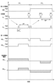
- FIG. 6 An example of a timing chart showing this driving method is shown in Fig. 6.
- This chart shows the potential change of the second electrode 140 and the potential change of the scanning line G and the signal line S over two frame periods (first frame period FP1 and second frame period FP2 ) out of a plurality of frame periods each having a fixed time.
- the time of each frame period is appropriately selected from the range of, for example, 1/180 seconds to 1 second.
- Each frame period includes m subframe periods SFP 1 to SFP m .
- a scanning signal is supplied from each scanning line G.
- the potential of the scanning signal becomes a potential that opens each element circuit (hereinafter, for convenience, this potential is referred to as High)
- a control signal is supplied from a signal line S to n radio wave reflecting elements 130 arranged in the row to which the scanning signal is supplied.
- the period during which control signals are supplied to all radio wave reflecting elements 130 in each frame period, that is, the time until all subframe periods SFP 1 to SFP m are completed, is the writing period WP.
- the potential of the control signal is determined by the direction in which the radio wave is reflected, so that the potential of the control signal supplied from one signal line may change periodically and stepwise for each subframe period, as shown in FIG. 6, for example.
- the absolute value of the potential of the control signal is appropriately selected from a range of 0 V or more and 20 V or less.
- the dielectric constant may be constant over the entire liquid crystal layer 136, and therefore the potential of the control signal may be constant in each frame period.
- the potential of the scanning line G becomes a potential that closes the element circuit (hereinafter, for convenience, this potential is referred to as Low).
- the element circuit maintains the potential of the first electrode 132 of each radio wave reflecting element 130 for a certain period (holding period HP).
- holding period HP ends in each frame period, all radio wave reflecting elements 130 are reset. That is, after the holding period HP, a scanning signal with a High potential is supplied from all scanning lines G to open the element circuit, and at the same time, a reset signal is supplied from the signal line S. This period is called the reset period RP.
- the potential of the reset signal is set so that the potential of the first electrode 132 becomes the potential of the common potential (COM) of the second electrode 140.
- a common potential is supplied to the second electrode 140. More specifically, either a positive potential (High) or a negative potential (Low) relative to a reference potential such as the ground potential is supplied to the second electrode 140 as the common potential.
- the absolute value of the potential supplied to the second electrode 140 may be selected, for example, from the range of 0V to 20V.
- the direction of reflection of radio waves is determined by the amount of change in the dielectric constant of the liquid crystal layer 136.
- common potential inversion driving (COM inversion driving) is adopted, which can increase the electric field strength by increasing the potential applied to the liquid crystal layer 136.
- the polarity of the common potential is changed every j frames.
- j is selected from natural numbers equal to or greater than 1, independent of m and n, and may be an odd or even number.
- the upper limit of j is, for example, 6.
- j is 1, and the radio wave reflecting device 100 is driven so that the common potential switches between High and Low for j frame periods, i.e., every frame period.
- the polarity of the control signal is also inverted every j frame period at the same time as the polarity inversion of the common potential. That is, when the common potential is Low (first frame period FP 1 in FIG. 6), a control signal having a positive potential with respect to the reference potential is supplied to the radio wave reflecting element 130 via the signal line S. On the other hand, when the common potential is High (second frame period FP 2 in FIG. 6), a control signal having a negative potential with respect to the reference potential is supplied to the radio wave reflecting element 130 via the signal line S.
- the signal line S 1 sequentially supplies positive potentials P 11 , P 21 , P 31 , . . . in the writing period WP of the first frame period FP 1 , and sequentially supplies negative potentials -P 11 , -P 21 , -P 31 , . . . in the writing period WP of the second frame period FP 2 .
- the potential of the reset signal if the polarity of the common potential is inverted every j frame periods, the polarity of the reset signal is also inverted every j frame periods. Therefore, the potential of the reset signal is Low during frame periods when the common potential is Low, and the potential of the reset signal is High during frame periods when the common potential is High.
- the scanning direction is reversed every k frame periods in order to suppress the row dependency of the magnitude of the effective voltage, which is the product of the voltage applied to the liquid crystal layer 136 and the application time, and to reduce the difference between rows of the effective voltage applied to the liquid crystal layer 136.
- the order of supplying the scanning signal to the scanning line G i.e., the order of supplying a High potential to open the element circuit, the same applies below
- scanning signals are supplied to m scanning lines G in either the first order of the first scanning line G1, the second scanning line G2, ..., to the mth scanning line, or the second order of the mth scanning line, the (m-1)th scanning line, ..., to the first scanning line.
- the first order and the second order are switched every k frame periods.
- k is a natural number equal to or greater than 1, independent of j, m, and n, and may be an even number or an odd number.
- the upper limit of k is, for example, 6.
- k and j may be the same or different. In the latter case, k may be greater than or less than j.
- k is 1, and the first order and the second order are switched every frame period. Therefore, in the first frame period FP1 and the second frame period FP2 , signal lines are supplied to the scanning lines G according to the first order and the second order, respectively.
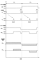
- Fig. 7 shows a timing chart including the potential change of the first electrode 132 and the electric field change occurring in the liquid crystal layer 136 when the radio wave reflecting device 100 is driven according to the example shown in Fig. 6.
- this timing chart for the purpose of facilitating understanding, the potential change of the first electrode 132 and the electric field change of the liquid crystal layer 136 of the radio wave reflecting elements RE11 and REm1 located in the first row, first column and the m-th row, first column are shown.
- the potential of the control signal supplied to the first electrode 132 is determined by the direction in which the radio wave is reflected, but for the sake of convenience, the potential of the control signal will be described as being High or Low here.
- a low common potential is supplied to the second electrode 140, and during that time, a scanning signal is supplied to the scanning line G according to the first order. Therefore, the potential of the first electrode 132 of the radio wave reflecting element RE11 located in the first row becomes high in the first subframe period SFP1 , and then the potential is maintained until the holding period HP ends, and returns to low in the reset period RP.
- the potential of the first electrode 132 of the radio wave reflecting element REm1 located in the mth row remains low until the mth subframe period SFPm, and becomes high in the mth subframe period SFPm . This potential is maintained until the holding period HP ends, and returns to low in the reset period RP.
- the polarity of the common potential is inverted and changes to High.
- all the first electrodes 132 that were at a Low potential at the end of the first frame period FP1 are capacitively coupled to the second electrodes 140 via the liquid crystal layer 136, so that their potentials become High.
- scanning signals are supplied to the scanning lines G in the second order.
- the polarity of the common potential is inverted, the polarity of the potential of the control signal is also inverted. Therefore, the potential of the first electrode 132 of the radio wave reflecting element REm1 to which writing is first performed in the second frame period FP2 is maintained at Low until the reset period RP.
- the potential of the first electrode 132 of the radio wave reflecting element RE11 which has changed to High due to capacitive coupling, returns to Low in the m -th subframe period SFPm, and the Low potential is maintained until the reset period RP.
- the first order is adopted during frame periods when the common potential is low, and the second order is adopted during frame periods when the common potential is high.
- the periods between the rows i.e., the periods of High and Low
- the periods between the rows are different between the radio wave reflecting elements RE11 and REm1 in each of the first frame period FP1 and the second frame period FP2 .
- the electric field generated in the liquid crystal layer 136 is determined by the potential difference between the first electrode 132 and the second electrode 140, the effective voltage applied to the liquid crystal layer 136 between the radio wave reflecting elements RE11 and REm1 in each of the first frame period FP1 and the second frame period FP2 is different, and the time during which the electric field exists is also different.
- the electric field is generated in the radio wave reflecting element RE11 from the first subframe period SFP1 to the end of the holding period HP, whereas the electric field is generated in the radio wave reflecting element REm1 from the m - th subframe period SFPm to the end of the holding period HP. Therefore, an electric field is generated for a longer time in the radio wave reflecting element RE11 than in the radio wave reflecting element REm1 .
- this state is reversed.
- the effective voltage and electric field applied to the liquid crystal layer 136 between the radio wave reflecting elements RE11 and REm1 are the same. Therefore, the difference in effective voltage and electric field between the first row and the m-th row is eliminated over a plurality of frame periods including the first frame period FP1 and the second frame period FP2 .
- the same can be said for the radio wave reflecting elements 130 located in the second row to the (m-1)-th row, so that the row dependency of the difference in effective voltage and electric field is eliminated in all columns by this scanning direction reversal driving.
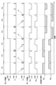
- FIG. 8 a timing chart for the case where the scanning direction inversion drive is not applied is shown in FIG. 8.
- the period in which the potential of the control signal is High is long for the radio wave reflecting element RE1
- the period in which the potential of the control signal is Low is also long for the radio wave reflecting element RE1 . Therefore, the effective voltage and electric field applied to the liquid crystal layer 136 in any frame period is larger for the radio wave reflecting element RE11 than for the radio wave reflecting element REm1 , and this difference is not eliminated even if it is integrated over a plurality of frame periods. Therefore, even if the same signal is input, the reflection phase that is actually set by the row is different, so that the radio wave cannot be reflected in the intended direction, and the reflection characteristics are deteriorated.
- the radio wave reflection device 100 is driven by scanning direction inversion driving, so that the effective voltage and electric field applied to the liquid crystal layer 136 are integrated over multiple frame periods to eliminate row dependency. This makes it possible to effectively suppress deterioration of the reflection characteristics.
- a reset period RP is provided after the end of the holding period HP, and the potentials of the first electrode 132 and the second electrode 140 are set to be the same or substantially the same.
- the potential of the first electrode 132 also shifts with the inversion of the common potential, but by setting this reset period RP, problems associated with the potential shift can be prevented. More specifically, for example, when the potential of the second electrode 140 inverts from Low to High, the potential of the first electrode 132 also rises due to capacitive coupling, but since the potential of the first electrode 132 is set to Low prior to the inversion of the common potential, this potential change is limited to a change from Low to High. The same is true in the reverse case. Therefore, potential changes that exceed the withstand voltages of various elements such as transistors and capacitive elements provided in the element circuit are prevented, and destruction of the element circuit can be prevented.
- the polarity of the common potential may be inverted every frame period, and the scanning direction may be inverted every several frame periods.
- the polarity of the common potential is inverted every frame period, but the scanning direction is inverted every two frame periods.
- the row dependency of the effective voltage and electric field applied to the liquid crystal layer 136 can be eliminated by integrating a plurality of frame periods (here, four frame periods including at least the first frame period FP1 to the fourth frame period FP4).
- the polarity of the common potential may be inverted every two or three frame periods, and the scanning direction may be inverted every frame period.
- FIG. 10 shows a case where j and k are 2 and 1, respectively
- FIG. 11 shows a case where j and k are 3 and 1 , respectively.
- the polarity of the common potential is inverted every two frame periods, but the scanning direction is inverted every frame period.
- the row dependency of the effective voltage and electric field applied to the liquid crystal layer 136 can be eliminated by integrating a plurality of frame periods (here, four frame periods including at least the first frame period FP1 to the fourth frame period FP4).
- the polarity of the common potential is inverted every three frame periods, but the scanning direction is inverted every frame period. Even in this case, the row dependency of the effective voltage and electric field applied to the liquid crystal layer 136 can be eliminated by integrating a plurality of frame periods (here, six frame periods including at least the first frame period FP1 to the sixth frame period FP6).
- the scanning direction may be reversed every several frame periods.
- a case where j and k are both 2 is shown in FIG. 12.
- the polarity of the common potential and the scanning direction are reversed every two frame periods.
- the row dependency of the effective voltage and electric field applied to the liquid crystal layer 136 can be eliminated by integrating several frame periods (here, four frame periods including at least the first frame period FP1 to the fourth frame period FP4).
- the scanning direction is reversed at the same time as the polarity of the common potential is reversed, and the scanning directions are opposite to each other between two consecutive frames in which the polarity of the common potential is reversed.
- the scanning direction may be the same over two consecutive frames in which the polarity of the common potential is reversed, and the polarity of the common potential may be the same between two consecutive frames in which the scanning direction is reversed.
- the driving method of the radio wave reflecting device 100 not only is the potential (common potential) of the second electrode 140 shared by the multiple radio wave reflecting elements 130 inverted every frame period or every multiple frame periods, but the order in which scanning signals are supplied to the scanning lines is also switched every frame period or every multiple frame periods.
- this driving method not only can a large electric field be generated in the liquid crystal layer 136, but the row dependency of the effective voltage and electric field applied to the liquid crystal layer 136 can be eliminated, and as a result, a deterioration in the reflection characteristics can be prevented.
- radio wave reflecting device 100: radio wave reflecting device, 102: substrate, 104: scanning line driving circuit, 106: signal line driving circuit, 108: terminal, 110: opposing substrate, 112: undercoat, 114: overcoat, 130: radio wave reflecting element, 132: first electrode, 134: first alignment film, 136: liquid crystal layer, 138: second alignment film, 140: second electrode, 150: transistor, 152: gate electrode, 154: gate insulating film, 156: semiconductor film, 158: terminal, 160: terminal, 162: interlayer insulating film, 164: planarizing film, 166: interlayer insulating film
Landscapes
- Physics & Mathematics (AREA)
- Electromagnetism (AREA)
- Liquid Crystal (AREA)
- Liquid Crystal Display Device Control (AREA)
Priority Applications (2)
| Application Number | Priority Date | Filing Date | Title |
|---|---|---|---|
| JP2024558663A JPWO2024105980A1 (https=) | 2022-11-15 | 2023-09-07 | |
| US19/177,785 US20250309553A1 (en) | 2022-11-15 | 2025-04-14 | Method for driving radio-wave reflector |
Applications Claiming Priority (2)
| Application Number | Priority Date | Filing Date | Title |
|---|---|---|---|
| JP2022182599 | 2022-11-15 | ||
| JP2022-182599 | 2022-11-15 |
Related Child Applications (1)
| Application Number | Title | Priority Date | Filing Date |
|---|---|---|---|
| US19/177,785 Continuation US20250309553A1 (en) | 2022-11-15 | 2025-04-14 | Method for driving radio-wave reflector |
Publications (1)
| Publication Number | Publication Date |
|---|---|
| WO2024105980A1 true WO2024105980A1 (ja) | 2024-05-23 |
Family
ID=91084254
Family Applications (1)
| Application Number | Title | Priority Date | Filing Date |
|---|---|---|---|
| PCT/JP2023/032663 Ceased WO2024105980A1 (ja) | 2022-11-15 | 2023-09-07 | 電波反射装置の駆動方法 |
Country Status (3)
| Country | Link |
|---|---|
| US (1) | US20250309553A1 (https=) |
| JP (1) | JPWO2024105980A1 (https=) |
| WO (1) | WO2024105980A1 (https=) |
Citations (4)
| Publication number | Priority date | Publication date | Assignee | Title |
|---|---|---|---|---|
| JP2004109824A (ja) * | 2002-09-20 | 2004-04-08 | Seiko Epson Corp | 電気光学装置、電気光学装置の駆動方法、電気光学装置の駆動回路および電子機器 |
| JP2005532590A (ja) * | 2002-07-05 | 2005-10-27 | サムスン エレクトロニクス カンパニー リミテッド | 液晶表示装置及びその駆動方法 |
| WO2017149646A1 (ja) * | 2016-03-01 | 2017-09-08 | 株式会社オルタステクノロジー | 液晶表示装置 |
| WO2022211035A1 (ja) * | 2021-03-31 | 2022-10-06 | 株式会社ジャパンディスプレイ | 電波反射板 |
-
2023
- 2023-09-07 JP JP2024558663A patent/JPWO2024105980A1/ja active Pending
- 2023-09-07 WO PCT/JP2023/032663 patent/WO2024105980A1/ja not_active Ceased
-
2025
- 2025-04-14 US US19/177,785 patent/US20250309553A1/en active Pending
Patent Citations (4)
| Publication number | Priority date | Publication date | Assignee | Title |
|---|---|---|---|---|
| JP2005532590A (ja) * | 2002-07-05 | 2005-10-27 | サムスン エレクトロニクス カンパニー リミテッド | 液晶表示装置及びその駆動方法 |
| JP2004109824A (ja) * | 2002-09-20 | 2004-04-08 | Seiko Epson Corp | 電気光学装置、電気光学装置の駆動方法、電気光学装置の駆動回路および電子機器 |
| WO2017149646A1 (ja) * | 2016-03-01 | 2017-09-08 | 株式会社オルタステクノロジー | 液晶表示装置 |
| WO2022211035A1 (ja) * | 2021-03-31 | 2022-10-06 | 株式会社ジャパンディスプレイ | 電波反射板 |
Also Published As
| Publication number | Publication date |
|---|---|
| JPWO2024105980A1 (https=) | 2024-05-23 |
| US20250309553A1 (en) | 2025-10-02 |
Similar Documents
| Publication | Publication Date | Title |
|---|---|---|
| US7227609B2 (en) | In-plane switching mode thin film transistor liquid crystal display device with wide viewing angle | |
| US8149369B2 (en) | In-plane switching mode LCD device | |
| JP3008928B2 (ja) | 液晶表示装置 | |
| KR100293436B1 (ko) | 횡전계방식액정표시장치 | |
| US7969519B2 (en) | Liquid crystal display device and method of fabricating the same | |
| KR20090015243A (ko) | 박막 트랜지스터 기판 및 이를 구비하는 액정 표시 장치 | |
| US20240243485A1 (en) | Intelligent reflecting surface | |
| US7599036B2 (en) | In-plane switching active matrix liquid crystal display apparatus | |
| US20090086118A1 (en) | Array substrate, display panel having the same and method of driving the same | |
| US20070002251A1 (en) | Thin film transistor array panel and method for manufacturing the same | |
| US20040207788A1 (en) | Liquid crystal display device | |
| KR100311531B1 (ko) | 횡전계방식액정표시장치및그제조방법 | |
| US6456352B1 (en) | Liquid crystal display device | |
| WO2024105980A1 (ja) | 電波反射装置の駆動方法 | |
| CN101201522B (zh) | 液晶显示设备及其制造方法 | |
| WO2024157610A1 (ja) | 電波反射装置 | |
| WO2024202779A1 (ja) | 電波反射装置および電波反射装置の駆動方法 | |
| JPH11194365A (ja) | 液晶表示素子及び液晶表示装置 | |
| US20250372872A1 (en) | Intelligent reflecting surface and method for driving the intelligent reflecting surface | |
| KR100268008B1 (ko) | 액정표시 소자 | |
| TWI400805B (zh) | 基板,具其之液晶顯示面板及具其之液晶顯示裝置 | |
| US20260018800A1 (en) | Intelligent reflecting surface | |
| US20150146124A1 (en) | Liquid crystal display and manufacturing method thereof | |
| KR101163396B1 (ko) | 횡전계모드 액정표시소자 및 그 제조방법 | |
| WO2025033055A1 (ja) | 電波反射装置 |
Legal Events
| Date | Code | Title | Description |
|---|---|---|---|
| 121 | Ep: the epo has been informed by wipo that ep was designated in this application |
Ref document number: 23891139 Country of ref document: EP Kind code of ref document: A1 |
|
| WWE | Wipo information: entry into national phase |
Ref document number: 2024558663 Country of ref document: JP |
|
| NENP | Non-entry into the national phase |
Ref country code: DE |
|
| 122 | Ep: pct application non-entry in european phase |
Ref document number: 23891139 Country of ref document: EP Kind code of ref document: A1 |