WO2024101006A1 - 半導体装置 - Google Patents
半導体装置 Download PDFInfo
- Publication number
- WO2024101006A1 WO2024101006A1 PCT/JP2023/034189 JP2023034189W WO2024101006A1 WO 2024101006 A1 WO2024101006 A1 WO 2024101006A1 JP 2023034189 W JP2023034189 W JP 2023034189W WO 2024101006 A1 WO2024101006 A1 WO 2024101006A1
- Authority
- WO
- WIPO (PCT)
- Prior art keywords
- region
- electrode
- film
- trench
- main surface
- Prior art date
- Legal status (The legal status is an assumption and is not a legal conclusion. Google has not performed a legal analysis and makes no representation as to the accuracy of the status listed.)
- Ceased
Links
Images











Classifications
-
- H—ELECTRICITY
- H10—SEMICONDUCTOR DEVICES; ELECTRIC SOLID-STATE DEVICES NOT OTHERWISE PROVIDED FOR
- H10D—INORGANIC ELECTRIC SEMICONDUCTOR DEVICES
- H10D62/00—Semiconductor bodies, or regions thereof, of devices having potential barriers
- H10D62/10—Shapes, relative sizes or dispositions of the regions of the semiconductor bodies; Shapes of the semiconductor bodies
- H10D62/124—Shapes, relative sizes or dispositions of the regions of semiconductor bodies or of junctions between the regions
- H10D62/126—Top-view geometrical layouts of the regions or the junctions
- H10D62/127—Top-view geometrical layouts of the regions or the junctions of cellular field-effect devices, e.g. multicellular DMOS transistors or IGBTs
-
- H—ELECTRICITY
- H10—SEMICONDUCTOR DEVICES; ELECTRIC SOLID-STATE DEVICES NOT OTHERWISE PROVIDED FOR
- H10D—INORGANIC ELECTRIC SEMICONDUCTOR DEVICES
- H10D12/00—Bipolar devices controlled by the field effect, e.g. insulated-gate bipolar transistors [IGBT]
-
- H—ELECTRICITY
- H10—SEMICONDUCTOR DEVICES; ELECTRIC SOLID-STATE DEVICES NOT OTHERWISE PROVIDED FOR
- H10D—INORGANIC ELECTRIC SEMICONDUCTOR DEVICES
- H10D12/00—Bipolar devices controlled by the field effect, e.g. insulated-gate bipolar transistors [IGBT]
- H10D12/411—Insulated-gate bipolar transistors [IGBT]
- H10D12/441—Vertical IGBTs
- H10D12/461—Vertical IGBTs having non-planar surfaces, e.g. having trenches, recesses or pillars in the surfaces of the emitter, base or collector regions
- H10D12/481—Vertical IGBTs having non-planar surfaces, e.g. having trenches, recesses or pillars in the surfaces of the emitter, base or collector regions having gate structures on slanted surfaces, on vertical surfaces, or in grooves, e.g. trench gate IGBTs
-
- H—ELECTRICITY
- H10—SEMICONDUCTOR DEVICES; ELECTRIC SOLID-STATE DEVICES NOT OTHERWISE PROVIDED FOR
- H10D—INORGANIC ELECTRIC SEMICONDUCTOR DEVICES
- H10D30/00—Field-effect transistors [FET]
- H10D30/60—Insulated-gate field-effect transistors [IGFET]
-
- H—ELECTRICITY
- H10—SEMICONDUCTOR DEVICES; ELECTRIC SOLID-STATE DEVICES NOT OTHERWISE PROVIDED FOR
- H10D—INORGANIC ELECTRIC SEMICONDUCTOR DEVICES
- H10D62/00—Semiconductor bodies, or regions thereof, of devices having potential barriers
- H10D62/10—Shapes, relative sizes or dispositions of the regions of the semiconductor bodies; Shapes of the semiconductor bodies
-
- H—ELECTRICITY
- H10—SEMICONDUCTOR DEVICES; ELECTRIC SOLID-STATE DEVICES NOT OTHERWISE PROVIDED FOR
- H10D—INORGANIC ELECTRIC SEMICONDUCTOR DEVICES
- H10D62/00—Semiconductor bodies, or regions thereof, of devices having potential barriers
- H10D62/10—Shapes, relative sizes or dispositions of the regions of the semiconductor bodies; Shapes of the semiconductor bodies
- H10D62/102—Constructional design considerations for preventing surface leakage or controlling electric field concentration
- H10D62/103—Constructional design considerations for preventing surface leakage or controlling electric field concentration for increasing or controlling the breakdown voltage of reverse-biased devices
- H10D62/105—Constructional design considerations for preventing surface leakage or controlling electric field concentration for increasing or controlling the breakdown voltage of reverse-biased devices by having particular doping profiles, shapes or arrangements of PN junctions; by having supplementary regions, e.g. junction termination extension [JTE]
- H10D62/106—Constructional design considerations for preventing surface leakage or controlling electric field concentration for increasing or controlling the breakdown voltage of reverse-biased devices by having particular doping profiles, shapes or arrangements of PN junctions; by having supplementary regions, e.g. junction termination extension [JTE] having supplementary regions doped oppositely to or in rectifying contact with regions of the semiconductor bodies, e.g. guard rings with PN or Schottky junctions
-
- H—ELECTRICITY
- H10—SEMICONDUCTOR DEVICES; ELECTRIC SOLID-STATE DEVICES NOT OTHERWISE PROVIDED FOR
- H10D—INORGANIC ELECTRIC SEMICONDUCTOR DEVICES
- H10D62/00—Semiconductor bodies, or regions thereof, of devices having potential barriers
- H10D62/10—Shapes, relative sizes or dispositions of the regions of the semiconductor bodies; Shapes of the semiconductor bodies
- H10D62/102—Constructional design considerations for preventing surface leakage or controlling electric field concentration
- H10D62/112—Constructional design considerations for preventing surface leakage or controlling electric field concentration for preventing surface leakage due to surface inversion layers, e.g. by using channel stoppers
-
- H—ELECTRICITY
- H10—SEMICONDUCTOR DEVICES; ELECTRIC SOLID-STATE DEVICES NOT OTHERWISE PROVIDED FOR
- H10D—INORGANIC ELECTRIC SEMICONDUCTOR DEVICES
- H10D62/00—Semiconductor bodies, or regions thereof, of devices having potential barriers
- H10D62/10—Shapes, relative sizes or dispositions of the regions of the semiconductor bodies; Shapes of the semiconductor bodies
- H10D62/17—Semiconductor regions connected to electrodes not carrying current to be rectified, amplified or switched, e.g. channel regions
- H10D62/393—Body regions of DMOS transistors or IGBTs
-
- H—ELECTRICITY
- H10—SEMICONDUCTOR DEVICES; ELECTRIC SOLID-STATE DEVICES NOT OTHERWISE PROVIDED FOR
- H10D—INORGANIC ELECTRIC SEMICONDUCTOR DEVICES
- H10D62/00—Semiconductor bodies, or regions thereof, of devices having potential barriers
- H10D62/60—Impurity distributions or concentrations
-
- H—ELECTRICITY
- H10—SEMICONDUCTOR DEVICES; ELECTRIC SOLID-STATE DEVICES NOT OTHERWISE PROVIDED FOR
- H10D—INORGANIC ELECTRIC SEMICONDUCTOR DEVICES
- H10D64/00—Electrodes of devices having potential barriers
- H10D64/01—Manufacture or treatment
- H10D64/011—Manufacture or treatment of electrodes ohmically coupled to a semiconductor
-
- H—ELECTRICITY
- H10—SEMICONDUCTOR DEVICES; ELECTRIC SOLID-STATE DEVICES NOT OTHERWISE PROVIDED FOR
- H10D—INORGANIC ELECTRIC SEMICONDUCTOR DEVICES
- H10D64/00—Electrodes of devices having potential barriers
- H10D64/111—Field plates
- H10D64/117—Recessed field plates, e.g. trench field plates or buried field plates
-
- H—ELECTRICITY
- H10—SEMICONDUCTOR DEVICES; ELECTRIC SOLID-STATE DEVICES NOT OTHERWISE PROVIDED FOR
- H10D—INORGANIC ELECTRIC SEMICONDUCTOR DEVICES
- H10D64/00—Electrodes of devices having potential barriers
- H10D64/20—Electrodes characterised by their shapes, relative sizes or dispositions
-
- H—ELECTRICITY
- H10—SEMICONDUCTOR DEVICES; ELECTRIC SOLID-STATE DEVICES NOT OTHERWISE PROVIDED FOR
- H10D—INORGANIC ELECTRIC SEMICONDUCTOR DEVICES
- H10D64/00—Electrodes of devices having potential barriers
- H10D64/20—Electrodes characterised by their shapes, relative sizes or dispositions
- H10D64/23—Electrodes carrying the current to be rectified, amplified, oscillated or switched, e.g. sources, drains, anodes or cathodes
- H10D64/232—Emitter electrodes for IGBTs
-
- H—ELECTRICITY
- H10—SEMICONDUCTOR DEVICES; ELECTRIC SOLID-STATE DEVICES NOT OTHERWISE PROVIDED FOR
- H10D—INORGANIC ELECTRIC SEMICONDUCTOR DEVICES
- H10D64/00—Electrodes of devices having potential barriers
- H10D64/20—Electrodes characterised by their shapes, relative sizes or dispositions
- H10D64/27—Electrodes not carrying the current to be rectified, amplified, oscillated or switched, e.g. gates
-
- H—ELECTRICITY
- H10—SEMICONDUCTOR DEVICES; ELECTRIC SOLID-STATE DEVICES NOT OTHERWISE PROVIDED FOR
- H10D—INORGANIC ELECTRIC SEMICONDUCTOR DEVICES
- H10D64/00—Electrodes of devices having potential barriers
- H10D64/20—Electrodes characterised by their shapes, relative sizes or dispositions
- H10D64/27—Electrodes not carrying the current to be rectified, amplified, oscillated or switched, e.g. gates
- H10D64/311—Gate electrodes for field-effect devices
- H10D64/411—Gate electrodes for field-effect devices for FETs
- H10D64/511—Gate electrodes for field-effect devices for FETs for IGFETs
- H10D64/517—Gate electrodes for field-effect devices for FETs for IGFETs characterised by the conducting layers
- H10D64/519—Gate electrodes for field-effect devices for FETs for IGFETs characterised by the conducting layers characterised by their top-view geometrical layouts
-
- H—ELECTRICITY
- H10—SEMICONDUCTOR DEVICES; ELECTRIC SOLID-STATE DEVICES NOT OTHERWISE PROVIDED FOR
- H10D—INORGANIC ELECTRIC SEMICONDUCTOR DEVICES
- H10D64/00—Electrodes of devices having potential barriers
- H10D64/60—Electrodes characterised by their materials
- H10D64/66—Electrodes having a conductor capacitively coupled to a semiconductor by an insulator, e.g. MIS electrodes
-
- H—ELECTRICITY
- H10—SEMICONDUCTOR DEVICES; ELECTRIC SOLID-STATE DEVICES NOT OTHERWISE PROVIDED FOR
- H10D—INORGANIC ELECTRIC SEMICONDUCTOR DEVICES
- H10D84/00—Integrated devices formed in or on semiconductor substrates that comprise only semiconducting layers, e.g. on Si wafers or on GaAs-on-Si wafers
-
- H—ELECTRICITY
- H10—SEMICONDUCTOR DEVICES; ELECTRIC SOLID-STATE DEVICES NOT OTHERWISE PROVIDED FOR
- H10D—INORGANIC ELECTRIC SEMICONDUCTOR DEVICES
- H10D84/00—Integrated devices formed in or on semiconductor substrates that comprise only semiconducting layers, e.g. on Si wafers or on GaAs-on-Si wafers
- H10D84/01—Manufacture or treatment
- H10D84/02—Manufacture or treatment characterised by using material-based technologies
- H10D84/03—Manufacture or treatment characterised by using material-based technologies using Group IV technology, e.g. silicon technology or silicon-carbide [SiC] technology
- H10D84/038—Manufacture or treatment characterised by using material-based technologies using Group IV technology, e.g. silicon technology or silicon-carbide [SiC] technology using silicon technology, e.g. SiGe
-
- H—ELECTRICITY
- H10—SEMICONDUCTOR DEVICES; ELECTRIC SOLID-STATE DEVICES NOT OTHERWISE PROVIDED FOR
- H10P—GENERIC PROCESSES OR APPARATUS FOR THE MANUFACTURE OR TREATMENT OF DEVICES COVERED BY CLASS H10
- H10P14/00—Formation of materials, e.g. in the shape of layers or pillars
- H10P14/40—Formation of materials, e.g. in the shape of layers or pillars of conductive or resistive materials
-
- H—ELECTRICITY
- H10—SEMICONDUCTOR DEVICES; ELECTRIC SOLID-STATE DEVICES NOT OTHERWISE PROVIDED FOR
- H10W—GENERIC PACKAGES, INTERCONNECTIONS, CONNECTORS OR OTHER CONSTRUCTIONAL DETAILS OF DEVICES COVERED BY CLASS H10
- H10W10/00—Isolation regions in semiconductor bodies between components of integrated devices
-
- H—ELECTRICITY
- H10—SEMICONDUCTOR DEVICES; ELECTRIC SOLID-STATE DEVICES NOT OTHERWISE PROVIDED FOR
- H10W—GENERIC PACKAGES, INTERCONNECTIONS, CONNECTORS OR OTHER CONSTRUCTIONAL DETAILS OF DEVICES COVERED BY CLASS H10
- H10W10/00—Isolation regions in semiconductor bodies between components of integrated devices
- H10W10/01—Manufacture or treatment
-
- H—ELECTRICITY
- H10—SEMICONDUCTOR DEVICES; ELECTRIC SOLID-STATE DEVICES NOT OTHERWISE PROVIDED FOR
- H10W—GENERIC PACKAGES, INTERCONNECTIONS, CONNECTORS OR OTHER CONSTRUCTIONAL DETAILS OF DEVICES COVERED BY CLASS H10
- H10W20/00—Interconnections in chips, wafers or substrates
- H10W20/01—Manufacture or treatment
-
- H—ELECTRICITY
- H10—SEMICONDUCTOR DEVICES; ELECTRIC SOLID-STATE DEVICES NOT OTHERWISE PROVIDED FOR
- H10W—GENERIC PACKAGES, INTERCONNECTIONS, CONNECTORS OR OTHER CONSTRUCTIONAL DETAILS OF DEVICES COVERED BY CLASS H10
- H10W20/00—Interconnections in chips, wafers or substrates
- H10W20/40—Interconnections external to wafers or substrates, e.g. back-end-of-line [BEOL] metallisations or vias connecting to gate electrodes
Definitions
- This disclosure relates to a semiconductor device.
- Patent Document 1 discloses a semiconductor device including a semiconductor substrate, multiple trench structures, and a gate pad portion.
- the multiple trench structures are formed on the surface of the semiconductor substrate.
- the gate pad portion is disposed on the semiconductor substrate so as to cover the multiple trench structures.
- the purpose of this disclosure is to provide a semiconductor device that can reduce leakage current.
- One embodiment of the present disclosure includes a chip having a first main surface and a second main surface opposite the first main surface, an active region provided on the first main surface, a peripheral region outside the active region and provided on the peripheral portion of the first main surface, a drift region of a first conductivity type formed inside the chip, a first medium concentration region of the first conductivity type as a carrier accumulation region formed in a surface layer portion of the drift region on the first main surface side in the active region and having a first conductivity type impurity concentration higher than that of the drift region, a channel region of a second conductivity type in the surface layer portion of the first main surface in the active region and disposed on the first main surface side of the first medium concentration region, a first high concentration region of the first conductivity type disposed in the surface layer portion of the channel region and having a first conductivity type impurity concentration higher than that of the first medium concentration region, and a first high concentration region of the first conductivity type extending from the first main surface to the first high concentration region, the channel region, and the first medium
- a semiconductor device includes a trench gate structure that reaches the drift region through a concentration region, a second medium concentration region of a first conductivity type selectively formed in a surface layer portion of the drift region on the first main surface side in the peripheral region, a second high concentration region of a first conductivity type as a channel stop region that is a surface layer portion of the first main surface in the peripheral region and is arranged on the first main surface side with respect to the second medium concentration region and has a first conductivity type impurity concentration higher than that of the second medium concentration region, a channel stop contact region of a second conductivity type formed in a surface layer portion of the second medium concentration region on the second high concentration region side, a channel stop electrode that is arranged on the first main surface in the peripheral region so as to cover the channel stop contact region, and a channel stop connection electrode that electrically connects the channel stop electrode and the channel stop contact region.
- This configuration can reduce leakage current.
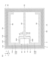
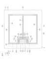
- FIG. 1 is a plan view showing a semiconductor device according to an embodiment.
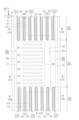
- FIG. 2 is a plan view showing the layout of the first main surface.
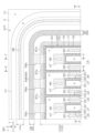
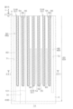
- FIG. 3 is an enlarged plan view showing the active region and the peripheral region.
- FIG. 4 is a cross-sectional view taken along line IV-IV shown in FIG.
- FIG. 5 is a cross-sectional view taken along line V-V shown in FIG.
- FIG. 6 is a cross-sectional view taken along the line VI-VI shown in FIG.
- FIG. 7 is an enlarged plan view showing the active and boundary regions.
- FIG. 8 is a cross-sectional view taken along line VIII-VIII shown in FIG.
- FIG. 9 is a cross-sectional view taken along line IX-IX shown in FIG.
- FIG. 1 is a plan view showing a semiconductor device according to an embodiment.
- FIG. 2 is a plan view showing the layout of the first main surface.
- FIG. 3 is an enlarged plan view showing the active region and the peripheral region.
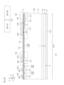
- FIG. 10A is a schematic cross-sectional view showing the structure of the inner peripheral part of the outer peripheral region.
- FIG. 10B is a schematic cross-sectional view showing the structure of a portion outside of FIG. 10A.
- FIG. 10C is an enlarged cross-sectional view showing a detailed structure of region XC in FIG. 10B.
- FIG. 10D is an enlarged cross-sectional view showing a detailed structure of region XD in FIG. 10B.
- FIG. 10E is an enlarged cross-sectional view showing a part of a semiconductor device according to a comparative example, and corresponds to FIG. 10D.
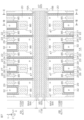
- FIG. 11 is an enlarged plan view showing the pad area.
- FIG. 12 is an enlarged plan view showing the gate resistor structure shown in FIG. FIG.
- FIG. 13 is an enlarged plan view showing an inner part of the gate resistor structure shown in FIG.
- FIG. 14 is an enlarged plan view showing one end of the gate resistor structure shown in FIG. 15 is an enlarged plan view showing the other end of the gate resistor structure shown in FIG. 16 is a cross-sectional view taken along line XVI-XVI shown in FIG. 13.
- FIG. 17 is a cross-sectional view taken along line XVII-XVII shown in FIG. 18 is a cross-sectional view taken along line XVIII-XVIII shown in FIG.
- FIG. 19 is a cross-sectional view taken along line XIX-XIX shown in FIG.
- FIG. 20 is a cross-sectional view taken along the line XX-XX shown in FIG.
- FIG. 21 is a cross-sectional view taken along line XXI-XXI shown in FIG. 15.
- FIG. 22 is a cross-sectional view taken along line XXII-XXII shown in FIG. 12.
- FIG. 23 is a plan view showing the layout of the resistance film, the gate electrode film, and the gate wiring film.
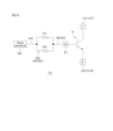
- FIG. 24 is an electrical circuit diagram showing a gate resistor structure, a gate terminal electrode, and a gate wiring electrode.
- FIG. 25 is a graph showing simulation results of leakage current Ics [A] versus collector-emitter voltage Vce [V] for each of the semiconductor device according to this embodiment and the semiconductor device according to the comparative example.
- this phrase includes a numerical value (shape) equal to the numerical value (shape) of the comparison target, as well as a numerical error (shape error) within a range of ⁇ 10% based on the numerical value (shape) of the comparison target.
- the words “first,” “second,” “third,” etc. are used, but these are symbols added to the names of each structure to clarify the order of explanation, and are not added with the intention of limiting the names of each structure.
- FIG. 1 is a plan view showing a semiconductor device 1A according to the first embodiment.
- FIG. 2 is a plan view showing the layout of a first main surface 3.
- FIG. 3 is an enlarged plan view showing an active region 6 and a peripheral region 9.
- FIG. 4 is a cross-sectional view taken along line IV-IV shown in FIG. 3.
- FIG. 5 is a cross-sectional view taken along line V-V shown in FIG. 3.
- FIG. 6 is a cross-sectional view taken along line VI-VI shown in FIG. 3.
- FIG. 7 is an enlarged plan view showing the active region 6 and the boundary region 8.
- FIG. 8 is a cross-sectional view taken along line VIII-VIII shown in FIG. 7.
- FIG. 9 is a cross-sectional view taken along line IX-IX shown in FIG. 7.
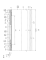
- FIG. 10A is a schematic cross-sectional view showing the structure of the inner peripheral portion of the outer peripheral region.
- FIG. 10B is a schematic cross-sectional view showing the structure of a portion further outboard than FIG. 10A.
- FIG. 10C is an enlarged cross-sectional view showing the detailed structure of region XC in FIG. 10B.
- FIG. 10D is an enlarged cross-sectional view showing the detailed structure of region XD in FIG. 10B.
- the semiconductor device 1A is an IGBT semiconductor device equipped with an IGBT (Insulated Gate Bipolar Transistor). With reference to Figures 1 to 10D, the semiconductor device 1A includes a chip 2 having a hexahedral shape (specifically, a rectangular parallelepiped shape). The chip 2 may be referred to as a "semiconductor chip.” In this embodiment, the chip 2 has a single-layer structure made of a silicon single crystal substrate (semiconductor substrate).
- the chip 2 has a first main surface 3 on one side, a second main surface 4 on the other side, and first to fourth side surfaces 5A to 5D connecting the first main surface 3 and the second main surface 4.
- the first main surface 3 and the second main surface 4 are formed in a quadrangular shape when viewed in a plan view from their normal direction Z (hereinafter simply referred to as "plan view").
- the normal direction Z is also the thickness direction of the chip 2.
- the first side surface 5A and the second side surface 5B extend in a first direction X along the first main surface 3 and face a second direction Y that intersects with the first direction X along the first main surface 3. Specifically, the second direction Y is perpendicular to the first direction X.
- the third side surface 5C and the fourth side surface 5D extend in the second direction Y and face the first direction X.
- the semiconductor device 1A includes a plurality of active regions 6 spaced apart on the first main surface 3.
- the plurality of active regions 6 include a first active region 6A and a second active region 6B.
- the first active region 6A is provided in an area on the first side surface 5A side of a line that crosses the center of the first main surface 3 in the first direction X.
- the second active region 6B is provided in an area on the second side surface 5B side of a line that crosses the center of the first main surface 3 in the first direction X.
- each active region 6 is formed in a polygonal shape having four sides parallel to the periphery of the chip 2 in a plan view.
- the planar shape of each active region 6 is arbitrary.
- the semiconductor device 1A includes an inactive region 7 provided in a region outside the multiple active regions 6 on the first main surface 3.
- the inactive region 7 includes a boundary region 8 and a peripheral region 9.
- the boundary region 8 is provided in a band shape extending in the first direction X in the region between the first active region 6A and the second active region 6B. In this embodiment, the boundary region 8 is located on a straight line that crosses the center of the first main surface 3 in the first direction X.
- the boundary region 8 includes a pad region 10 having a relatively large width in the second direction Y, and a street region 11 having a width in the second direction Y that is smaller than the width of the pad region 10.
- the pad region 10 may be referred to as a "first boundary region” or a "wide region”.
- the street region 11 may be referred to as a "second boundary region", a "line region” or a "narrow region”.
- the pad region 10 is provided in an area on one side in the first direction X (the third side surface 5C side). In this embodiment, the pad region 10 is located on a straight line that crosses the center of the first main surface 3 in the first direction X in a plan view, and is provided in a rectangular shape near the center of the third side surface 5C.
- the street region 11 is provided in an area on the other side in the first direction X (the fourth side surface 5D side) of the pad region 10. In this embodiment, the street region 11 is pulled out in a strip shape from the pad region 10 toward the fourth side surface 5D side, and is located on a straight line that crosses the center of the first main surface 3 in the first direction X.
- the peripheral region 9 is provided on the periphery of the chip 2 so as to collectively surround the multiple active regions 6.
- the peripheral region 9 is provided in a ring shape (a square ring shape in this embodiment) extending along the periphery (first to fourth side faces 5A to 5D) of the chip 2.
- the peripheral region 9 is connected to the pad region 10 on one side (the third side face 5C side) of the first main surface 3, and is connected to the street region 11 on the other side (the fourth side face 5D side) of the first main surface 3.
- the semiconductor device 1A includes an n-type (first conductivity type) drift region 12 formed inside the chip 2.
- the drift region 12 is formed throughout the entire interior of the chip 2.
- the chip 2 is made of an n-type semiconductor substrate (n-type semiconductor chip), and the drift region 12 is formed using the n-type chip 2.
- the semiconductor device 1A includes an n-type buffer region 13 formed in a surface layer of the second main surface 4.
- the buffer region 13 is formed in a layer extending along the second main surface 4 over the entire area of the second main surface 4.
- the buffer region 13 has a higher n-type impurity concentration than the drift region 12.
- the presence or absence of the buffer region 13 is optional, and a configuration without the buffer region 13 may be adopted.
- the semiconductor device 1A includes a p-type (second conductivity type) collector region 14 formed in a surface layer portion of the second main surface 4.
- the collector region 14 is formed in a surface layer portion on the second main surface 4 side of the buffer region 13.
- the collector region 14 is formed in a layer shape extending along the second main surface 4 over the entire area of the second main surface 4.
- the collector region 14 is exposed from the second main surface 4 and parts of the first to fourth side surfaces 5A to 5D.
- the semiconductor device 1A includes a plurality of trench isolation structures 15 formed on the first main surface 3 so as to separate a plurality of active regions 6.
- a gate potential is applied to the plurality of trench isolation structures 15.
- the trench isolation structures 15 may also be referred to as “trench gate isolation structures” or “trench gate connection structures.”
- the plurality of trench isolation structures 15 include a first trench isolation structure 15A on the first active region 6A side and a second trench isolation structure 15B on the second active region 6B side.
- the first trench isolation structure 15A surrounds the first active region 6A and separates the first active region 6A from the boundary region 8 and the outer peripheral region 9.
- the first trench isolation structure 15A is formed in a polygonal ring shape having four sides parallel to the periphery of the chip 2 in a plan view.
- the first trench isolation structure 15A has a bent portion that separates the pad region 10 and street region 11 of the boundary region 8 in a plan view.
- the second trench isolation structure 15B surrounds the second active region 6B and separates the second active region 6B from the boundary region 8 and the outer peripheral region 9.
- the second trench isolation structure 15B is formed in a polygonal ring shape having four sides parallel to the periphery of the chip 2 in a plan view.
- the second trench isolation structure 15B has a bent portion that separates the pad region 10 and street region 11 of the boundary region 8 in a plan view.
- the trench isolation structure 15 preferably has a width less than the width of the street region 11.
- the width of the trench isolation structure 15 is the width in a direction perpendicular to the direction in which the trench isolation structure 15 extends.
- the width of the trench isolation structure 15 may be 0.1 ⁇ m or more and 2.5 ⁇ m or less.
- the width of the trench isolation structure 15 is preferably 0.3 ⁇ m or more and 1 ⁇ m or less.
- the width of the trench isolation structure 15 is preferably 0.4 ⁇ m or more and 0.7 ⁇ m or less.
- the trench isolation structure 15 may have a depth of 1 ⁇ m or more and 20 ⁇ m or less.
- the depth of the trench isolation structure 15 is preferably 4 ⁇ m or more and 10 ⁇ m or less.
- the trench isolation structure 15 includes an isolation trench 16, an isolation insulating film 17, and an isolation buried electrode 18.
- the isolation trench 16 is formed in the first main surface 3 and defines the wall surface of the trench isolation structure 15.
- the isolation insulating film 17 covers the wall surface of the isolation trench 16 in a film-like manner.
- the isolation insulating film 17 may include at least one of a silicon oxide film, a silicon nitride film, and an aluminum oxide film.
- the isolation insulating film 17 preferably has a single-layer structure made of a single insulating film. It is particularly preferable that the isolation insulating film 17 includes a silicon oxide film made of an oxide of the chip 2.
- the isolation buried electrode 18 is buried in the isolation trench 16 with the isolation insulating film 17 in between.
- the isolation buried electrode 18 may include conductive polysilicon. A gate potential is applied to the isolation buried electrode 18.
- the semiconductor device 1A includes an IGBT structure Tr (transistor structure) formed in each active region 6.
- the IGBT structure Tr is not formed in the inactive region 7. Since the configuration on the second active region 6B side (the configuration of the IGBT structure Tr) is substantially the same as the configuration on the first active region 6A side (the configuration of the IGBT structure Tr), the configuration on the first active region 6A side will be described below.
- the configuration on the second active region 6B side is linearly symmetrical to the configuration on the first active region 6A side across the boundary region 8.
- the description of the structure on the second active region 6B side is omitted, as the description of the structure on the first active region 6A side applies.
- the semiconductor device 1A includes an n-type first medium concentration region 19 as a carrier accumulation region formed in the surface layer of the first main surface 3 in the first active region 6A.
- the first medium concentration region 19 is formed in the surface layer of the drift region 12 on the first main surface 3 side.
- the first medium concentration region 19 extends in a layer shape along the first main surface 3 and is connected to the inner peripheral wall of the trench isolation structure 15.
- the first medium concentration region 19 is formed shallower than the trench isolation structure 15 and has a bottom located on the first main surface 3 side of the bottom wall of the trench isolation structure 15.
- the bottom of the first medium concentration region 19 is preferably located on the first main surface 3 side of the intermediate depth range of the trench isolation structure 15.
- the thickness of the first medium concentration region 19 may be about 2 ⁇ m.
- the first intermediate concentration region 19 has a higher n-type impurity concentration than the drift region 12.
- the drift region 12 may be referred to as the "first drift region,” and the first intermediate concentration region 19 may be referred to as the "second drift region.”
- the first intermediate concentration region 19 is formed to reduce the apparent resistivity of the drift region 12 and reduce conduction losses by accumulating holes from the p-type collector region 14.
- the n-type impurity concentration of drift region 12 gradually decreases from the surface of drift region 12 on the first main surface 3 side toward the surface of drift region 12 on the second main surface 4 side.
- the n-type impurity concentration of drift region 12 is preferably, for example, 1.0 ⁇ 10 13 cm -3 or more and 1.0 ⁇ 10 15 cm -3 or less.
- the n-type impurity concentration of first intermediate concentration region 19 is preferably, for example, 1.0 ⁇ 10 15 cm -3 or more.
- the n-type impurity concentration of first intermediate concentration region 19 may be, for example, 1.0 ⁇ 10 15 cm -3 or more and 1.0 ⁇ 10 17 cm -3 or less.
- the semiconductor device 1A includes a p-type channel region 20 formed in the surface layer of the first main surface 3 in the first active region 6A.
- the channel region 20 may be referred to as a "body region” or a "base region”.
- the channel region 20 is formed in the surface layer of the first intermediate concentration region 19 on the first main surface 3 side.
- the channel region 20 extends in a layered manner along the first main surface 3 and is connected to the inner peripheral wall of the trench isolation structure 15.
- the channel region 20 is formed shallower than the trench isolation structure 15 and has a bottom located on the first main surface 3 side of the bottom wall of the trench isolation structure 15. It is preferable that the bottom of the channel region 20 is located on the first main surface 3 side of the intermediate depth range of the trench isolation structure 15.
- the thickness of the channel region 20 may be about 1 ⁇ m.
- the semiconductor device 1A includes a plurality of first trench structures 21 formed on the first main surface 3 in the first active region 6A.
- a gate potential is applied to the plurality of first trench structures 21.
- the first trench structures 21 may be referred to as "trench gate structures.”
- the plurality of first trench structures 21 penetrate the channel region 20 to reach the drift region 12.
- the plurality of first trench structures 21 are arranged at intervals in the first direction X in a plan view, and are each formed in a band shape extending in the second direction Y. In other words, the plurality of first trench structures 21 are arranged in a stripe shape extending in the second direction Y.
- Each first trench structure 21 has one end on the boundary region 8 side and the other end on the outer periphery region 9 side in the longitudinal direction (second direction Y).
- One end and the other end of the multiple first trench structures 21 are mechanically and electrically connected to the trench isolation structure 15.
- the multiple first trench structures 21, together with the trench isolation structure 15, form a ladder-shaped trench structure.
- the connection portion between the first trench structure 21 and the trench isolation structure 15 may be considered as part of the trench isolation structure 15 and/or part of the first trench structure 21.
- the spacing between the multiple first trench structures 21 is preferably less than the width of the street region 11.
- the width of the first trench structure 21 is preferably less than the width of the street region 11.
- the width of the first trench structure 21 is the width in a direction perpendicular to the direction in which the first trench structure 21 extends.
- the width of the first trench structure 21 may be 0.1 ⁇ m or more and 2.5 ⁇ m or less.
- the width of the first trench structure 21 is preferably 0.3 ⁇ m or more and 1 ⁇ m or less.
- the width of the first trench structure 21 is 0.4 ⁇ m or more and 0.7 ⁇ m or less. It is preferable that the width of the first trench structure 21 is approximately equal to the width of the trench isolation structure 15.
- the first trench structure 21 may have a depth of 1 ⁇ m or more and 20 ⁇ m or less. It is preferable that the depth of the first trench structure 21 is 4 ⁇ m or more and 10 ⁇ m or less. It is preferable that the depth of the first trench structure 21 is approximately equal to the depth of the trench isolation structure 15.
- the first trench structure 21 includes a first trench 22, a first insulating film 23, and a first buried electrode 24.
- the first trench 22 is formed in the first main surface 3 and defines the wall surface of the first trench structure 21.
- the first trench 22 communicates with the isolation trench 16 at both ends in the second direction Y.
- the sidewall of the first trench 22 communicates with the sidewall of the isolation trench 16, and the bottom wall of the first trench 22 communicates with the bottom wall of the isolation trench 16.
- the first insulating film 23 covers the wall surface of the first trench 22 in a film-like manner.
- the first insulating film 23 may include at least one of a silicon oxide film, a silicon nitride film, and an aluminum oxide film. It is preferable that the first insulating film 23 has a single-layer structure consisting of a single insulating film.
- the first insulating film 23 includes a silicon oxide film made of an oxide of the chip 2.
- the first insulating film 23 is made of the same insulating film as the isolation insulating film 17.
- the first insulating film 23 is connected to the isolation insulating film 17 at the communicating portion between the isolation trench 16 and the first trench 22.
- the first buried electrode 24 is buried in the first trench 22 with the first insulating film 23 sandwiched therebetween.
- the first buried electrode 24 may contain conductive polysilicon.
- a gate potential is applied to the first buried electrode 24.
- the first buried electrode 24 is mechanically and electrically connected to the isolated buried electrode 18 at the communicating portion between the isolation trench 16 and the first trench 22.
- the semiconductor device 1A includes a plurality of second trench structures 25 formed in the regions between adjacent first trench structures 21 in the first main surface 3 of the first active region 6A.
- the second trench structures 25 may be referred to as "emitter trench structures.”
- Each second trench structure 25 is formed at a distance from the plurality of first trench structures 21 in the first direction X in a plan view, and is formed in a square ring shape extending in the second direction Y.
- the width of the second trench structure 25 is preferably less than the width of the street region 11.
- the width of the second trench structure 25 is the width in a direction perpendicular to the direction in which the second trench structure 25 extends.
- the width of the second trench structure 25 may be 0.1 ⁇ m or more and 2.5 ⁇ m or less.
- the width of the second trench structure 25 is preferably 0.3 ⁇ m or more and 1 ⁇ m or less.
- the width of the second trench structure 25 is particularly preferably 0.4 ⁇ m or more and 0.7 ⁇ m or less.
- the width of the second trench structure 25 is preferably approximately equal to the width of the first trench structure 21.
- the second trench structure 25 may have a depth of 1 ⁇ m or more and 20 ⁇ m or less.
- the depth of the second trench structure 25 is preferably 4 ⁇ m or more and 10 ⁇ m or less.
- the depth of the second trench structure 25 is preferably approximately equal to the depth of the first trench structure 21.
- the second trench structure 25 includes a second trench 26, a second insulating film 27, and a second buried electrode 28.
- the second trench 26 is formed in the first main surface 3 and defines the wall surface of the second trench structure 25.
- the second insulating film 27 covers the wall surface of the second trench 26 in a film-like manner.
- the second insulating film 27 may include at least one of a silicon oxide film, a silicon nitride film, and an aluminum oxide film. It is preferable that the second insulating film 27 has a single-layer structure consisting of a single insulating film. It is particularly preferable that the second insulating film 27 includes a silicon oxide film consisting of an oxide of the chip 2. In this embodiment, the second insulating film 27 is made of the same insulating film as the first insulating film 23.
- the second buried electrode 28 is buried in the second trench 26 with the second insulating film 27 sandwiched therebetween.
- the second buried electrode 28 may include conductive polysilicon.
- An emitter potential is applied to the second buried electrode 28.
- the semiconductor device 1A includes a plurality of n-type emitter regions 29 formed in a surface layer portion of the channel region 20 in the first active region 6A.
- the emitter regions 29 are an example of a "first high concentration region” in this disclosure and may be referred to as a "first high concentration region”.
- the plurality of emitter regions (first high concentration regions) 29 each have a higher n-type impurity concentration than the first intermediate concentration region 19.
- the plurality of emitter regions 29 are formed on both sides of the plurality of first trench structures 21, respectively.
- the n-type impurity concentration of the emitter regions 29 is preferably, for example, not less than 1.0 ⁇ 10 19 cm -3 and not more than 1.0 ⁇ 10 21 cm -3 .
- the multiple emitter regions 29 are each formed in a band shape extending along the multiple first trench structures 21 in a planar view.
- the multiple emitter regions 29 may be formed at intervals along the multiple first trench structures 21 in a planar view.
- the multiple emitter regions 29 are formed in the region between the first trench structure 21 and the second trench structure 25 so as to be connected to the first trench structure 21 and the second trench structure 25. It is preferable that the emitter regions 29 are not formed in the region between the trench isolation structure 15 and the outermost second trench structure 25.
- the semiconductor device 1A includes a plurality of contact holes 30 formed in the first main surface 3 so as to expose the emitter region 29 in the first active region 6A.
- the contact holes 30 are an example of a "first contact hole” in this disclosure.
- the plurality of contact holes 30 are formed on both sides of the plurality of first trench structures 21 at intervals from the plurality of first trench structures 21.
- the plurality of contact holes 30 may each be formed in a tapered shape in which the opening width narrows from the opening toward the bottom wall.
- the multiple contact holes 30 penetrate the emitter region 29 so as to reach the channel region 20.
- the multiple contact holes 30 may be spaced away from the bottom of the emitter region 29 toward the first main surface 3 so as not to reach the channel region 20.
- the multiple contact holes 30 are each formed in a band shape extending along the multiple first trench structures 21 in a plan view. In terms of the longitudinal direction (second direction Y), it is preferable that the multiple contact holes 30 are shorter than the multiple first trench structures 21. It is particularly preferable that the multiple contact holes 30 are shorter than the multiple second trench structures 25.
- the semiconductor device 1A includes a plurality of p-type channel contact regions 31 formed in a surface layer portion of the channel region 20 of the first active region 6A in a region different from the plurality of emitter regions 29.
- the plurality of channel contact regions 31 have a higher p-type impurity concentration than the channel region 20.
- the plurality of channel contact regions 31 are each formed in a band shape extending along the corresponding contact hole 30 in a plan view.
- the bottoms of the plurality of channel contact regions 31 are each formed in a region between the bottom wall of the corresponding contact hole 30 and the bottom of the channel region 20.
- the p-type impurity concentration of the channel region 20 is preferably, for example, not less than 1.0 ⁇ 10 16 cm ⁇ 3 and not more than 1.0 ⁇ 10 18 cm ⁇ 3
- the p-type impurity concentration of the channel contact region 31 is preferably, for example, not less than 1.0 ⁇ 10 18 cm ⁇ 3 and not more than 1.0 ⁇ 10 20 cm ⁇ 3 .
- the semiconductor device 1A includes a plurality of p-type floating regions 32 formed in regions surrounded by a plurality of second trench structures 25 in the surface layer portion of the first main surface 3 of the first active region 6A.
- the plurality of floating regions 32 are formed in an electrically floating state.
- an emitter potential may be applied to the plurality of floating regions 32.
- the plurality of floating regions 32 have a higher p-type impurity concentration than the channel region 20.
- Each floating region 32 extends in a layer shape along the first main surface 3 and is connected to the inner peripheral wall of each second trench structure 25. It is preferable that each floating region 32 is formed deeper than the middle part of the depth range of the second trench structure 25. In this embodiment, each floating region 32 is formed deeper than the second trench structure 25 and has a portion that covers the bottom wall of the second trench structure 25.
- the first active region 6A includes, as an IGBT structure Tr, a channel region 20, a plurality of first trench structures 21, a plurality of second trench structures 25, a plurality of emitter regions 29, a plurality of contact holes 30, a plurality of channel contact regions 31, and a plurality of floating regions 32.
- the second active region 6B includes, as an IGBT structure Tr, a channel region 20, a plurality of first trench structures 21, a plurality of second trench structures 25, a plurality of emitter regions 29, a plurality of contact holes 30, a plurality of channel contact regions 31, and a plurality of floating regions 32.
- the semiconductor device 1A includes a p-type boundary well region 40 formed in the surface layer of the first main surface 3 in the boundary region 8.
- the boundary well region 40 has a higher p-type impurity concentration than the channel region 20.
- the boundary well region 40 may have a lower p-type impurity concentration than the channel region 20.
- the boundary well region 40 is formed in a band shape extending in the first direction X along the boundary region 8 in a plan view.
- the boundary well region 40 is formed in a layer shape extending along the first main surface 3 in the region sandwiched between the first trench isolation structure 15A and the second trench isolation structure 15B, and is exposed from the first main surface 3.
- the boundary well region 40 is formed in the region sandwiched between the multiple first trench structures 21 on the first active region 6A side and the multiple first trench structures 21 on the second active region 6B side.
- the boundary well region 40 includes a first boundary well region 40A formed in the pad region 10, and a second boundary well region 40B formed in the street region 11.
- the first boundary well region 40A has a relatively large region width in the second direction Y.
- the first boundary well region 40A is formed in a polygonal shape (a square shape in this embodiment) in a plan view. It is preferable that the first boundary well region 40A is formed over the entire pad region 10.
- the second boundary well region 40B has a width in the second direction Y that is smaller than the width of the first boundary well region 40A, and is pulled out in a strip from the first boundary well region 40A toward the street region 11.
- the second boundary well region 40B is located on a straight line that crosses the center of the first main surface 3 in the first direction X.
- the second boundary well region 40B extends in a strip so as to be located on one side (the third side surface 5C side) and the other side (the fourth side surface 5D side) of the straight line that crosses the center of the first main surface 3 in the second direction Y.
- the boundary well region 40 is preferably formed deeper than the channel region 20. It is particularly preferable that the boundary well region 40 is formed deeper than the multiple trench isolation structures 15 (multiple first trench structures 21). In this embodiment, the boundary well region 40 has a width in the second direction Y that is greater than the width of the boundary region 8, and is pulled out from the boundary region 8 into the multiple active regions 6.
- the boundary well region 40 is connected to multiple trench isolation structures 15 adjacent in the second direction Y.
- the boundary well region 40 has a portion that covers the bottom walls of the multiple trench isolation structures 15.
- the boundary well region 40 has a portion that crosses the multiple trench isolation structures 15 and covers the bottom walls of the multiple first trench structures 21.
- the boundary well region 40 covers the sidewalls of the trench isolation structure 15 and the sidewalls of the trench structures in the active regions 6, and is connected to each channel region 20 in the surface portion of the first main surface 3.
- the depth of the boundary well region 40 may be 1 ⁇ m or more and 20 ⁇ m or less.
- the depth of the boundary well region 40 is preferably 5 ⁇ m or more and 10 ⁇ m or less.
- the semiconductor device 1A includes a p-type peripheral well region 41 formed in the surface layer of the first main surface 3 in the peripheral region 9.
- the peripheral well region 41 has a higher p-type impurity concentration than the channel region 20.
- the peripheral well region 41 may have a lower p-type impurity concentration than the channel region 20. It is preferable that the p-type impurity concentration of the peripheral well region 41 is approximately equal to the p-type impurity concentration of the boundary well region 40.
- the peripheral well region 41 is formed in a layer extending along the first main surface 3 and is exposed from the first main surface 3.
- the peripheral well region 41 is formed at a distance inward from the periphery (first to fourth side surfaces 5A to 5D) of the first main surface 3.
- the peripheral well region 41 is formed in a band shape extending along the multiple active regions 6 in a planar view.
- the peripheral well region 41 is formed in a ring shape (a square ring in this embodiment) that collectively surrounds the multiple active regions 6 in a planar view.
- the peripheral well region 41 is preferably formed deeper than the channel region 20. It is particularly preferable that the peripheral well region 41 is formed deeper than the multiple trench isolation structures 15 (multiple first trench structures 21). The peripheral well region 41 preferably has a depth approximately equal to that of the boundary well region 40.
- the peripheral well region 41 is connected to the multiple trench isolation structures 15.
- the peripheral well region 41 has a portion that covers the bottom walls of the multiple trench isolation structures 15.
- the peripheral well region 41 is pulled out from the peripheral region 9 into the multiple active regions 6.
- the peripheral well region 41 has a portion that crosses the multiple trench isolation structures 15 and covers the bottom walls of the multiple first trench structures 21.
- the peripheral well region 41 covers the sidewalls of the trench isolation structure 15 and the sidewalls of the multiple first trench structures 21 in each active region 6, and is connected to multiple channel regions 20 in the surface portion of the first main surface 3.
- the peripheral well region 41 is connected to the boundary well region 40 at the connection portion of the boundary region 8 and the peripheral region 9. In other words, the peripheral well region 41, together with the boundary well region 40, defines multiple active regions 6.
- the semiconductor device 1A includes at least one (in this embodiment, multiple) p-type field region 42 formed in the surface layer of the first main surface 3 in the peripheral region 9.
- the number of field regions 42 is arbitrary and may be 1 to 20 (typically 3 to 10).
- the multiple field regions 42 may have a higher p-type impurity concentration than the channel region 20.
- the multiple field regions 42 may have a higher p-type impurity concentration than the peripheral well region 41.
- the multiple field regions 42 may have a lower p-type impurity concentration than the peripheral well region 41.
- the multiple field regions 42 may have a p-type impurity concentration approximately equal to that of the peripheral well region 41.
- the multiple field regions 42 are formed in an electrically floating state.
- the multiple field regions 42 are formed in the region between the periphery of the chip 2 and the peripheral well region 41, spaced apart from the periphery of the chip 2 and the peripheral well region 41.
- the multiple field regions 42 are formed in a band shape extending along the peripheral well region 41 in a plan view.
- the multiple field regions 42 are formed in a ring shape (square ring shape) surrounding the peripheral well region 41 in a plan view.
- the multiple field regions 42 are preferably formed deeper than the channel region 20.
- the multiple field regions 42 may be formed to a depth approximately equal to that of the peripheral well region 41.
- the multiple field regions 42 may be formed shallower than the peripheral well region 41.
- the multiple field regions 42 may be formed to a constant depth.
- the spacing between the multiple field regions 42 may gradually increase toward the peripheral edge of the chip 2.
- Each of the multiple field regions 42 has a width smaller than the width of the peripheral well region 41.
- the outermost field region 42 of the multiple field regions 42 may be formed wider than the other field regions 42.
- the semiconductor device 1A includes at least one (in this embodiment, multiple) p-type field contact region 111 formed in the surface layer portion on the first main surface 3 side of each field region 42.
- two field contact regions 111 are formed for one field region 42.
- the field contact region 111 has the same p-type impurity concentration as the channel contact region 31.
- Such a field contact region 111 can be formed simultaneously with the channel contact region 31, for example, in the process of forming the channel contact region 31.
- the semiconductor device 1A includes an n-type second medium concentration region 121 formed in the surface layer of the first main surface 3 at a distance from the multiple field regions 42 toward the periphery of the chip 2 in the outer periphery region 9.
- the second medium concentration region 121 has a higher n-type impurity concentration than the drift region 12.
- the second medium concentration region 121 has the same n-type impurity concentration as the first medium concentration region 19 serving as a carrier accumulation region.
- the second medium concentration region 121 is formed in a band shape extending along the periphery of the chip 2 in a plan view.
- the second medium concentration region 121 is formed in a ring shape (quadratic ring shape) surrounding a plurality of field regions 42 in a plan view.
- the second medium concentration region 121 may be exposed from the first to fourth side faces 5A to 5D.
- the second medium concentration region 121 is formed in an electrically floating state.
- the depth position of the bottom surface of the second medium concentration region 121 is equal to the depth position of the bottom surface of the first medium concentration region 19.
- Such a second medium concentration region 121 can be formed simultaneously with the first medium concentration region 19, for example, in the process of forming the first medium concentration region 19.
- the semiconductor device 1A includes an n-type second high concentration region 43 as a channel stop region formed in the surface layer portion on the first main surface 3 side of the second medium concentration region 121.
- the surface of the second high concentration region 43 on the second main surface 4 side is covered by the second medium concentration region 121.
- the second high concentration region 43 is a surface layer portion on the first main surface 3 side, and is disposed on the first main surface 3 side with respect to the second medium concentration region 121.
- the second high concentration region 43 has a higher n-type impurity concentration than the second medium concentration region 121.
- the second high concentration region 43 has the same n-type impurity concentration as the emitter region (first high concentration region) 29.
- Such a second high concentration region 43 can be formed simultaneously with the emitter region 29, for example, in the process of forming the emitter region 29.
- the second high concentration region 43 is formed in a band shape extending along the periphery of the chip 2 in a plan view.
- the second high concentration region 43 is formed in a ring shape (quadratic ring shape) surrounding the multiple field regions 42 in a plan view.
- the second high concentration region 43 may be exposed from the first to fourth side faces 5A to 5D.
- the inner peripheral edge of the bottom surface of the second medium concentration region 121 is covered by the second high concentration region 43.
- the inner peripheral edge of the second medium concentration region 121 is located closer to the field region 42 than the inner peripheral edge of the second high concentration region 43.
- the second high concentration region 43 is formed in an electrically floating state.
- the semiconductor device 1A includes at least one (in this embodiment, multiple) p-type channel stop contact region 122 formed in a region different from the second high concentration region 43 in the surface layer portion of the second medium concentration region 121 on the first main surface 3 side.
- the channel stop contact region 122 is formed in the surface layer portion of the second medium concentration region 121 on the second high concentration region 43 side.
- a part of the channel stop contact region 122 may be formed in the second high concentration region 43.
- the channel stop contact region 122 may be formed at the boundary between the second high concentration region 43 and the second medium concentration region 121, spanning them.
- the bottom surface of the channel stop contact region 122 is covered by the second medium concentration region 121.
- two channel stop contact regions 122 are formed.
- the channel stop contact region 122 has the same p-type impurity concentration as the channel contact region 31.
- Such a channel stop contact region 122 can be formed simultaneously with the channel contact region 31, for example, in the process of forming the channel contact region 31.
- the semiconductor device 1A includes a main surface insulating film 45 that selectively covers the first main surface 3.
- the main surface insulating film 45 selectively covers the first main surface 3 in the active region 6, the boundary region 8, and the peripheral region 9.
- the main surface insulating film 45 may include at least one of a silicon oxide film, a silicon nitride film, and an aluminum oxide film.
- the main surface insulating film 45 preferably has a single-layer structure made of a single insulating film. It is particularly preferable that the main surface insulating film 45 includes a silicon oxide film made of an oxide of the chip 2. In this embodiment, the main surface insulating film 45 is made of the same insulating film as the first insulating film 23 (isolation insulating film 17). The main surface insulating film 45 covers the first main surface 3 so as to expose the trench isolation structure 15, the first trench structure 21, and the second trench structure 25.
- the main surface insulating film 45 is connected to the isolation insulating film 17, the first insulating film 23, and the second insulating film 27, and exposes the isolation buried electrode 18, the first buried electrode 24, and the second buried electrode 28.
- the main surface insulating film 45 selectively covers the boundary well region 40, the peripheral well region 41, the field region 42, the second high concentration region 43, and the second medium concentration region 121 in the boundary region 8 and the peripheral region 9.
- the semiconductor device 1A includes a field insulating film 46 that selectively covers the first main surface 3 in the peripheral region 9.
- the main surface insulating film 45 and the field insulating film 46 are examples of a "surface insulating film" in this disclosure.
- the field insulating film 46 may include at least one of a silicon oxide film, a silicon nitride film, and an aluminum oxide film.
- the field insulating film 46 is thicker than the main surface insulating film 45.
- the field insulating film 46 includes a first field insulating film 131, a plurality of second field insulating films 132, and a third field insulating film 133.
- the first field insulating film 131 is formed on the first main surface 33, straddling the outer peripheral edge of the peripheral well region 41 and the inner peripheral edge of the innermost field region 42.
- the first field insulating film 131 is formed in a ring shape extending along the peripheral well region 41.
- the second field insulating film 132 is formed on the first main surface 33, straddling the outer peripheral edge of the inner field region 42 of two adjacent field regions 42 and the inner peripheral edge of the outer field region 42.
- Each second field insulating film 132 is formed in a ring shape extending along the inner field region 42 of the corresponding two field regions 42.
- the third field insulating film 133 is formed on the first main surface 33 so as to cover the region from a position close to the outer peripheral edge of the outermost field region 42 to the vicinity of the second medium concentration region 121.
- the third field insulating film 133 is formed at a distance from the second medium concentration region 121 towards the outermost field region 42.
- the third field insulating film 133 is formed in a ring shape extending along the outermost field region 42.
- the inner edge of the first field insulating film 131 is connected to the outer edge of the main surface insulating film 45 on the outer periphery well region 41.
- the outer edge of the first field insulating film 131 is connected to the inner edge of the main surface insulating film 45 that covers the middle part of the width of the innermost field region 42.
- the inner edge of the second field insulating film 132 that spans two adjacent field regions 42 is connected to the outer edge of the main surface insulating film 45 that covers the middle part of the width of the inner field region 42, and the outer edge of the second field insulating film 132 is connected to the inner edge of the main surface insulating film 45 that covers the middle part of the width of the outer field region 42.
- the inner edge of the third field insulating film 133 is connected to the outer edge of the main surface insulating film 45 that covers the middle part of the width of the outermost field region 42.
- the outer edge of the third field insulating film 133 is connected to the inner edge of the main surface insulating film 45 that is formed closer to the periphery of the chip 2.
- the semiconductor device 1A includes a plurality of emitter electrode films 47 arranged on the first main surface 3 so as to cover the plurality of second trench structures 25 in the active region 6.
- the plurality of emitter electrode films 47 are arranged on the main surface insulating film 45.
- the plurality of emitter electrode films 47 may include conductive polysilicon.
- the multiple emitter electrode films 47 cover both ends of the multiple second trench structures 25 in the second direction Y.
- the multiple emitter electrode films 47 are formed in a band shape extending in the second direction Y in the region between the corresponding second trench structures 25 and trench isolation structures 15.
- the multiple emitter electrode films 47 are formed at intervals from the trench isolation structures 15 toward the second trench structures 25.
- the multiple emitter electrode films 47 face the channel region 20 with the main surface insulating film 45 in between.
- the multiple emitter electrode films 47 are each formed integrally with the second buried electrodes 28 of the multiple second trench structures 25.
- the multiple emitter electrode films 47 are each made up of a portion of the second buried electrode 28 that is pulled out in a film-like form onto the first main surface 3 (main surface insulating film 45).
- the multiple emitter electrode films 47 may also be formed separately from the second buried electrodes 28.
- FIG. 11 is an enlarged plan view showing the pad region 10.
- FIG. 12 is an enlarged plan view showing the gate resistance structure 50 shown in FIG. 11.
- FIG. 13 is an enlarged plan view showing the inner part of the gate resistance structure 50 shown in FIG. 12.
- FIG. 14 is an enlarged plan view showing one end of the gate resistance structure 50 shown in FIG. 12.
- FIG. 15 is an enlarged plan view showing the other end of the gate resistance structure 50 shown in FIG. 12.
- FIG. 16 is a cross-sectional view taken along line XVI-XVI shown in FIG. 13.
- FIG. 17 is a cross-sectional view taken along line XVII-XVII shown in FIG. 13.
- FIG. 18 is a cross-sectional view taken along line XVIII-XVIII shown in FIG. 13.
- FIG. 19 is a cross-sectional view taken along line XIX-XIX shown in FIG. 13.
- FIG. 20 is a cross-sectional view taken along line XX-XX shown in FIG. 14.
- FIG. 21 is a cross-sectional view taken along line XXI-XXI in FIG. 15.
- FIG. 22 is a cross-sectional view taken along line XXII-XXII in FIG. 12.
- FIG. 23 is a plan view showing the layout of the resistance film 60, gate electrode film 64, and gate wiring film 65.
- FIG. 24 is an electrical circuit diagram showing the gate resistance structure 50, gate terminal electrode 90, and gate wiring electrode 93.
- the semiconductor device 1A includes a gate resistance structure 50 formed in the pad region 10.
- the gate resistance structure 50 constitutes a gate resistance RG for the gate of the IGBT (first trench structure 21 of the IGBT structure Tr).
- the gate resistance structure 50 includes a plurality of trench resistance structures 51 formed on the first main surface 3 in the pad region 10. A gate potential is applied to the plurality of trench resistance structures 51, but the plurality of trench resistance structures 51 do not contribute to channel control.
- the multiple gate resistance structures 50 form a first trench group 52 and a second trench group 53.
- the first trench group 52 includes multiple first trench resistance structures 51A that form part of the multiple trench resistance structures 51, and is provided on one side in the second direction Y (the first side surface 5A side).
- the number of first trench resistance structures 51A is arbitrary and is adjusted based on the resistance value to be achieved.
- the first trench group 52 may include 2 to 100 first trench resistance structures 51A.
- the number of first trench resistance structures 51A is preferably 50 or less.
- the number of first trench resistance structures 51A may be 25 or less.
- the number of first trench resistance structures 51A is preferably 5 or more.
- the gate resistance structure 50 may include a single first trench resistance structure 51A instead of the first trench group 52.
- the first trench group 52 is provided in a region on one side (first side surface 5A) in the second direction Y of a straight line that crosses the center of the first main surface 3 in the first direction X.
- the first trench group 52 is preferably arranged in the pad region 10 so as to be biased toward the active region 6 (street region 11) rather than the peripheral region 9.
- the first trench group 52 is arranged at intervals from the center of the pad region 10 toward the active region 6 (street region 11).
- the multiple first trench resistance structures 51A are formed on the first main surface 3 at intervals from the multiple trench isolation structures 15 (multiple first trench structures 21).
- the multiple first trench resistance structures 51A are arranged at intervals in the first direction X in a plan view, and are each formed in a band shape extending in the second direction Y. In other words, the multiple first trench resistance structures 51A are arranged in a stripe shape extending in the second direction Y.
- the multiple first trench resistance structures 51A have one end on one side in the second direction Y (the first side surface 5A side) and the other end on the other side in the second direction Y (the second side surface 5B side).
- the multiple first trench resistance structures 51A are formed at intervals from the bottom of the boundary well region 40 (first boundary well region 40A) toward the first main surface 3 so as to be located within the boundary well region 40 (first boundary well region 40A), and face the drift region 12 across a portion of the boundary well region 40. In other words, the multiple first trench resistance structures 51A do not penetrate the boundary well region 40 (first boundary well region 40A).
- the spacing between the multiple first trench resistance structures 51A is preferably less than the width of the street region 11.
- the spacing between the multiple first trench resistance structures 51A is preferably approximately equal to the spacing between the first trench structure 21 and the second trench structure 25.
- the spacing between the multiple first trench resistance structures 51A may be smaller than the spacing between the first trench structure 21 and the second trench structure 25.
- the spacing between the multiple first trench resistance structures 51A may be larger than the spacing between the first trench structure 21 and the second trench structure 25.
- the width of the first trench resistance structure 51A is preferably less than the width of the street region 11.
- the width of the first trench resistance structure 51A is a width in a direction perpendicular to the direction in which the first trench resistance structure 51A extends.
- the width of the first trench resistance structure 51A may be 0.1 ⁇ m or more and 2.5 ⁇ m or less.
- the width of the first trench resistance structure 51A is preferably 0.3 ⁇ m or more and 1 ⁇ m or less. It is particularly preferable that the width of the first trench resistance structure 51A is 0.4 ⁇ m or more and 0.7 ⁇ m or less. It is preferable that the width of the first trench resistance structure 51A is approximately equal to the width of the first trench structure 21.
- the first trench resistance structure 51A may have a depth of 1 ⁇ m or more and 20 ⁇ m or less. It is preferable that the depth of the first trench resistance structure 51A is 4 ⁇ m or more and 10 ⁇ m or less. It is preferable that the depth of the first trench resistance structure 51A is approximately equal to the depth of the first trench structure 21.
- the second trench group 53 includes a plurality of second trench resistance structures 51B that form part of the plurality of trench resistance structures 51, and are spaced apart from the first trench group 52 on the other side in the second direction Y (the second side surface 5B side).
- the number of second trench resistance structures 51B is arbitrary and is adjusted based on the resistance value to be achieved. For example, when a resistance value approximately equal to the resistance value on the first trench group 52 side is to be realized, the second trench group 53 may include the same number of second trench resistance structures 51B as the number of first trench resistance structures 51A.
- the second trench group 53 may include a number of second trench resistance structures 51B different from the number of first trench resistance structures 51A.
- the number of second trench resistance structures 51B may be less than the number of first trench resistance structures 51A.
- the number of second trench resistance structures 51B may be greater than the number of first trench resistance structures 51A.
- the second trench group 53 may include 2 to 100 second trench resistance structures 51B.
- the number of second trench resistance structures 51B is preferably 50 or less.
- the number of second trench resistance structures 51B may be 25 or less.
- the number of second trench resistance structures 51B is preferably 5 or more.
- the semiconductor device 1A may include a single second trench resistance structure 51B instead of the second trench group 53.
- the second trench group 53 is provided in a region on the other side in the second direction Y (second side surface 5B) of a straight line that crosses the center of the first main surface 3 in the first direction X.
- the second trench group 53 faces the first trench group 52 in the second direction Y.
- the second trench group 53 is preferably arranged so as to be biased toward the active region 6 side (street region 11 side) rather than the outer periphery region 9 in the pad region 10.
- the second trench group 53 is arranged at intervals from the center of the pad region 10 toward the active region 6 side (street region 11 side).
- the second trench resistance structures 51B are formed on the first main surface 3 at intervals from the trench isolation structures 15 (the first trench structures 21).
- the second trench resistance structures 51B are arranged at intervals in the first direction X in a plan view, and are each formed in a band shape extending in the second direction Y.
- the multiple second trench resistance structures 51B are arranged in a stripe pattern extending in the second direction Y.
- the multiple second trench resistance structures 51B each face the multiple first trench resistance structures 51A in a one-to-one correspondence in the second direction Y.
- the multiple second trench resistance structures 51B are each arranged in the same straight line as the multiple first trench resistance structures 51A.
- the multiple second trench resistance structures 51B each have one end on one side in the second direction Y (the first side surface 5A side) and the other end on the other side in the second direction Y (the second side surface 5B side).
- the second trench resistance structures 51B are formed at intervals from the bottom of the boundary well region 40 (first boundary well region 40A) toward the first main surface 3 so as to be located within the boundary well region 40 (first boundary well region 40A), and face the drift region 12 across a portion of the boundary well region 40. In other words, the second trench resistance structures 51B do not penetrate the boundary well region 40 (first boundary well region 40A).
- the spacing between the multiple second trench resistance structures 51B is preferably less than the width of the street region 11.
- the spacing between the multiple second trench resistance structures 51B is preferably approximately equal to the spacing between adjacent first trench structures 21 and second trench structures 25.
- the spacing between the multiple second trench resistance structures 51B may be smaller than the spacing between the first trench structures 21 and second trench structures 25.
- the spacing between the multiple second trench resistance structures 51B may be larger than the spacing between the first trench structures 21 and second trench structures 25.
- the spacing between the multiple second trench resistance structures 51B may be smaller than the spacing between the multiple first trench resistance structures 51A.
- the spacing between the multiple second trench resistance structures 51B may be larger than the spacing between the multiple first trench resistance structures 51A. It is preferable that the spacing between the multiple second trench resistance structures 51B is approximately equal to the spacing between the multiple first trench resistance structures 51A.
- the width of the second trench resistance structure 51B is preferably less than the width of the street region 11.
- the width of the second trench resistance structure 51B is the width in a direction perpendicular to the direction in which the second trench resistance structure 51B extends.
- the width of the second trench resistance structure 51B may be 0.1 ⁇ m or more and 2.5 ⁇ m or less.
- the width of the second trench resistance structure 51B is preferably 0.3 ⁇ m or more and 1 ⁇ m or less. It is particularly preferable that the width of the second trench resistance structure 51B is 0.4 ⁇ m or more and 0.7 ⁇ m or less.
- the width of the second trench resistance structure 51B is preferably approximately equal to the width of the first trench resistance structure 51A.
- the second trench resistance structure 51B has a length in the second direction Y that is approximately equal to the length of the first trench resistance structure 51A.
- the second trench resistance structure 51B may be longer than the first trench resistance structure 51A in the second direction Y.
- the second trench resistance structure 51B may be shorter than the first trench resistance structure 51A in the second direction Y. The length of the first trench resistance structure 51A and the length of the second trench resistance structure 51B are adjusted according to the resistance value to be achieved.
- the second trench resistance structure 51B may have a depth of 1 ⁇ m or more and 20 ⁇ m or less.
- the depth of the second trench resistance structure 51B is preferably 4 ⁇ m or more and 10 ⁇ m or less.
- the depth of the second trench resistance structure 51B is preferably approximately equal to the depth of the first trench resistance structure 51A (first trench structure 21).
- the trench resistance structure 51 includes a resistive trench 54, a resistive insulating film 55, and a resistive buried electrode 56.
- the resistive trench 54 is formed in the first main surface 3, and defines the wall surface of the trench resistance structure 51.
- the resistive insulating film 55 covers the wall surface of the resistive trench 54 in the form of a film.
- the resistive insulating film 55 is connected to the main surface insulating film 45 on the first main surface 3.
- the resistive insulating film 55 may include at least one of a silicon oxide film, a silicon nitride film, and an aluminum oxide film. It is preferable that the resistive insulating film 55 has a single-layer structure made of a single insulating film. It is particularly preferable that the resistive insulating film 55 includes a silicon oxide film made of an oxide of the chip 2.
- the resistor-buried electrode 56 is buried in the resistor trench 54 with a resistor insulating film 55 sandwiched therebetween.
- the resistor-buried electrode 56 may contain conductive polysilicon. A gate potential is applied to the resistor-buried electrode 56.
- the gate resistor structure 50 includes a space region 57 defined in the pad region 10 between the first trench group 52 and the second trench group 53.
- the space region 57 is formed by a flat portion of the first main surface 3 in the region between the other ends of the multiple first trench resistor structures 51A and one ends of the multiple second trench resistor structures 51B.
- the space region 57 is partitioned into a rectangular shape in a plan view.
- the space region 57 exposes the boundary well region 40 from the first main surface 3.
- the space region 57 is formed on a straight line that crosses the center of the first main surface 3 in the first direction X in a plan view, and faces the street region 11 in the first direction X.
- the space region 57 has a space width along the second direction Y.
- the space width is larger than the width in the first direction X of the first trench resistance structure 51A (second trench resistance structure 51B).
- the space width is larger than the distance between two first trench resistance structures 51A (second trench resistance structures 51B) adjacent to each other in the first direction X.
- the space width is preferably larger than the width in the first direction X of the first trench group 52 (second trench group 53).
- the space width may be smaller than the width in the first direction X of the first trench group 52 (second trench group 53).
- the space width is preferably smaller than the length in the second direction Y of the first trench group 52 (second trench group 53).
- the space width may be approximately equal to the width in the second direction Y of the street region 11.
- the space width may be larger than the width in the second direction Y of the street region 11.
- the space width may be smaller than the width in the second direction Y of the street region 11.
- the gate resistor structure 50 includes a resistive film 60 arranged on the first main surface 3 so as to cover the multiple trench resistor structures 51 in the pad region 10. Specifically, the resistive film 60 is arranged on the main surface insulating film 45.
- the resistive film 60 includes at least one of a conductive polysilicon film and an alloy film.
- the alloy film may include alloy crystals composed of metallic elements and non-metallic elements.
- the alloy film may include at least one of a CrSi film, a CrSiN film, a CrSiO film, a TaN film, and a TiN film.
- the resistive film 60 includes conductive polysilicon.
- the thickness of the resistive film 60 is adjusted as appropriate depending on the resistance value to be achieved. It is preferable that the thickness of the resistive film 60 is equal to or less than the depth of the first trench resistance structure 51A (second trench resistance structure 51B). It is particularly preferable that the thickness of the resistive film 60 is less than the depth of the first trench resistance structure 51A (second trench resistance structure 51B).
- the thickness of the resistive film 60 is preferably 0.5 times or more the width of the first trench resistance structure 51A (second trench resistance structure 51B).
- the thickness of the resistive film 60 may be 0.05 ⁇ m or more and 2.5 ⁇ m or less.
- the thickness of the resistive film 60 is preferably 0.5 ⁇ m or more and 1.5 ⁇ m or less.
- the thickness of the resistive film 60 may be 0.1 nm or more and 100 nm or less.
- the resistive film 60 is formed in a band shape extending in the second direction Y, and has a first end 60A on one side in the second direction Y (the first side surface 5A side) and a second end 60B on the other side in the second direction Y (the second side surface 5B side).
- the resistive film 60 has a width in the first direction X that is greater than the width in the first direction X of the first trench group 52 (second trench group 53).
- the width of the resistive film 60 may be less than the space width. Of course, the width of the resistive film 60 may be greater than or equal to the space width. It is preferable that the resistive film 60 has a uniform width in the first direction X.
- the resistive film 60 has a portion located on one side (first side surface 5A side) and a portion located on the other side (second side surface 5B side) in the second direction Y with respect to a line that crosses the center of the first main surface 3 in the first direction X.
- the resistive film 60 faces the first active region 6A, the second active region 6B, and the street region 11 in the first direction X.
- the resistive film 60 faces the multiple trench isolation structures 15, the multiple first trench structures 21, and the multiple second trench structures 25 in the first direction X.
- the resistive film 60 has a first covering portion 61 covering the space region 57, a second covering portion 62 covering the first trench group 52, and a third covering portion 63 covering the second trench group 53.
- the first covering portion 61 is a portion that covers the first main surface 3 in the area outside the first trench group 52 (plurality of first trench resistance structures 51A) and the second trench group 53 (plurality of second trench resistance structures 51B).
- the first covering portion 61 is located in the middle between the first end portion 60A and the second end portion 60B, and faces the boundary well region 40 across the main surface insulating film 45 in the thickness direction.
- the second covering portion 62 forms the first end 60A of the resistive film 60 and covers all of the first trench resistance structures 51A.
- the second covering portion 62 forms the first end 60A on the outer side (the peripheral edge side of the pad region 10) of one end of the multiple first trench resistance structures 51A.
- the first end 60A faces the first covering portion 61 across the first trench group 52 in a plan view.
- the second covering portion 62 is connected to the resistor-embedded electrodes 56 of the multiple first trench resistance structures 51A and faces the boundary well region 40 across the main surface insulating film 45 in the thickness direction.
- the third covering portion 63 forms the second end portion 60B of the resistive film 60 and covers all the second trench resistance structures 51B.
- the third covering portion 63 forms the second end portion 60B on the outer side (the peripheral side of the pad region 10) of the other ends of the multiple second trench resistance structures 51B.
- the second end portion 60B faces the first covering portion 61 across the second trench group 53 in a plan view.
- the third covering portion 63 is connected to the resistor-embedded electrodes 56 of the multiple second trench resistance structures 51B and faces the boundary well region 40 across the main surface insulating film 45 in the thickness direction.
- the resistive film 60 is formed integrally with the resistor-buried electrodes 56 of the multiple first trench resistor structures 51A in the second covering portion 62, and is formed integrally with the resistor-buried electrodes 56 of the multiple second trench resistor structures 51B in the third covering portion 63.
- the resistive film 60 is formed by a portion of the resistor-buried electrode 56 that is extended in the form of a film onto the first main surface 3 (main surface insulating film 45).
- the resistive film 60 may be formed separately from the resistor-buried electrode 56.
- the semiconductor device 1A includes a gate electrode film 64 disposed on the first main surface 3 so as to be adjacent to the resistive film 60. Specifically, the gate electrode film 64 is disposed on the main surface insulating film 45.
- the gate electrode film 64 includes at least one of a conductive polysilicon film and an alloy film.
- the alloy film may include alloy crystals composed of a metallic element and a non-metallic element.
- the alloy film may include at least one of a CrSi film, a CrSiN film, a CrSiO film, a TaN film, and a TiN film.
- the gate electrode film 64 is preferably formed of the same resistive material as the resistive film 60. In this embodiment, the gate electrode film 64 includes conductive polysilicon. The gate electrode film 64 preferably has a thickness approximately equal to that of the resistive film 60.
- the gate electrode film 64 is disposed on the main surface insulating film 45 at a distance from the resistive film 60 toward the inner side of the pad region 10 (the third side surface 5C side), and is physically separated from the resistive film 60.
- the gate electrode film 64 is formed at a distance from the multiple trench isolation structures 15 toward the inner side of the pad region 10 in a plan view.
- the gate electrode film 64 faces the boundary well region 40 (first boundary well region 40A) across the main surface insulating film 45.
- the gate electrode film 64 is formed in a polygonal shape (a square shape in this embodiment) in a plan view. In this embodiment, the gate electrode film 64 is formed in a rectangular shape extending in the second direction Y along the resistive film 60.
- the semiconductor device 1A includes a gate wiring film 65 arranged on the first main surface 3 adjacent to the resistive film 60 so as to face the gate electrode film 64 with the resistive film 60 in between.
- the gate wiring film 65 is arranged on the main surface insulating film 45.
- the gate wiring film 65 includes at least one of a conductive polysilicon film and an alloy film.
- the alloy film may include alloy crystals composed of a metallic element and a non-metallic element.
- the alloy film may include at least one of a CrSi film, a CrSiN film, a CrSiO film, a TaN film, and a TiN film.
- the gate wiring film 65 is preferably formed of the same resistive material as the resistive film 60. In this embodiment, the gate wiring film 65 includes conductive polysilicon. The gate wiring film 65 preferably has a thickness approximately equal to that of the resistive film 60.
- the gate wiring film 65 is disposed on the main surface insulating film 45 at a distance from the gate electrode film 64, and is physically separated from the gate electrode film 64.
- the gate wiring film 65 has a first connection portion connected to the first end 60A of the resistive film 60, and a second connection portion connected to the second end 60B of the resistive film 60.
- the gate wiring film 65 is electrically connected to the multiple trench resistance structures 51 via the resistive film 60. Specifically, the gate wiring film 65 is electrically connected to the multiple first trench resistance structures 51A between the first covering portion 61 and the second covering portion 62 of the resistive film 60, and is electrically connected to the multiple second trench resistance structures 51B between the second covering portion 62 and the third covering portion 63 of the resistive film 60.
- the gate wiring film 65 includes a first lower wiring portion 66, a second lower wiring portion 67, and a third lower wiring portion 68.
- the first lower wiring portion 66 is routed to the pad region 10. Specifically, the first lower wiring portion 66 surrounds the resistive film 60 and the gate electrode film 64 in the pad region 10 from multiple directions (three directions in this embodiment).
- the first lower wiring portion 66 includes a first lower line portion 69 and multiple second lower line portions 70A, 70B.
- the first lower line portion 69 is arranged on the street region 11 side of the resistive film 60 in the pad region 10.
- the first lower line portion 69 is arranged on the first main surface 3 adjacent to the resistive film 60 so as to face the gate electrode film 64 across the resistive film 60 in a plan view.
- the first lower line portion 69 faces the boundary well region 40 (first boundary well region 40A) across the main surface insulating film 45 in the thickness direction.
- the first lower line portion 69 is formed in a band shape extending in the second direction Y along the resistive film 60.
- the first lower line portion 69 has a length in the second direction Y that is greater than the length of the resistive film 60 and the length of the gate electrode film 64.
- the first lower line portion 69 has one end on one side in the second direction Y (the first side surface 5A side) and the other end on the other side in the second direction Y (the second side surface 5B side).
- the multiple second lower line portions 70A, 70B include a second lower line portion 70A on one side and a second lower line portion 70B on the other side.
- the second lower line portion 70A is arranged in a region on one side (first side surface 5A side) of the resistive film 60 and the gate electrode film 64 in the pad region 10 in the second direction Y.
- the second lower line portion 70B is arranged in a region on the other side (second side surface 5B side) of the resistive film 60 and the gate electrode film 64 in the pad region 10 in the second direction Y.
- the second lower line portion 70A is formed in a band shape extending in the first direction X, and has one end connected to one end of the first lower line portion 69, and the other end located on the peripheral side (third side surface 5C side) of the chip 2.
- the second lower line portion 70A is further connected to the first end 60A of the resistive film 60, and is formed at a distance from the gate electrode film 64.
- the second lower line portion 70A constitutes a first connection portion for the first end 60A.
- the second lower line portion 70A faces the boundary well region 40 (first boundary well region 40A) across the main surface insulating film 45 in the thickness direction.
- the second lower line portion 70B is formed in a band shape extending in the first direction X, and has one end connected to the other end of the first lower line portion 69, and the other end located on the peripheral side (third side surface 5C side) of the chip 2.
- the other side second lower line portion 70B is further connected to the second end 60B of the resistive film 60, and is formed at a distance from the gate electrode film 64.
- the second lower line portion 70B constitutes a second connection portion for the second end portion 60B.
- the other second lower line portion 70B faces the one second lower line portion 70A across the gate electrode film 64.
- the other second lower line portion 70B faces the boundary well region 40 (first boundary well region 40A) across the main surface insulating film 45 in the thickness direction.
- the second lower wiring portion 67 is routed to the street region 11. Specifically, the second lower wiring portion 67 is pulled out from the first lower wiring portion 66 to the street region 11. More specifically, the second lower wiring portion 67 is pulled out from the inner portion (the center portion in this embodiment) of the first lower line portion 69 to the street region 11, and is formed in a band shape extending in the first direction X.
- the second lower wiring portion 67 crosses the center of the chip 2.
- the second lower wiring portion 67 extends in a band shape so as to be located in an area on one side (the third side surface 5C side) and an area on the other side (the fourth side surface 5D side) of the first direction X with respect to a straight line that crosses the center of the first main surface 3 in the second direction Y.
- the second lower wiring portion 67 has one end connected to the first lower line portion 69 (the first lower wiring portion 66) on one side of the first direction X, and the other end on the other side of the first direction X.
- the second lower wiring portion 67 faces the boundary well region 40 (second boundary well region 40B) across the main surface insulating film 45 in the thickness direction.
- the second lower wiring portion 67 has a width greater than the width of the street region 11 in the second direction Y, and is drawn out from the street region 11 to the multiple active regions 6.
- the second lower wiring portion 67 covers the multiple trench isolation structures 15 in the multiple active regions 6.
- the second lower wiring portion 67 also covers the ends of the first trench structures 21 in the active regions 6. As a result, the second lower wiring portion 67 is electrically connected to the isolated buried electrodes 18 and the first buried electrodes 24, and transmits the gate potential to the isolated buried electrodes 18 and the first buried electrodes 24.
- the second lower wiring portion 67 is integrally formed with the multiple isolated buried electrodes 18 and the multiple first buried electrodes 24.
- the second lower wiring portion 67 is composed of a portion of the multiple isolated buried electrodes 18 and a portion of the multiple first buried electrodes 24 that are pulled out in a film-like manner onto the first main surface 3 (main surface insulating film 45).
- the second lower wiring portion 67 may be formed separately from the multiple isolated buried electrodes 18 and the multiple first buried electrodes 24.
- the third lower wiring portion 68 is routed to the outer peripheral region 9. Specifically, the third lower wiring portion 68 is pulled out from the first lower wiring portion 66 to the outer peripheral region 9. More specifically, the third lower wiring portion 68 is pulled out from the other ends of the multiple second lower line portions 70A, 70B to one side (first side surface 5A side) and the other side (second side surface 5B side) of the outer peripheral region 9, and is formed in a band shape extending along the outer peripheral region 9.
- the third lower wiring portion 68 sandwiches multiple active regions 6.
- the third lower wiring portion 68 extends along the periphery (first side surfaces 5A-5D) of the chip 2 so as to surround the multiple active regions 6 in a planar view, and is connected to the other end of the second lower wiring portion 67.
- the third lower wiring portion 68, together with the second lower wiring portion 67 surrounds the multiple active regions 6.
- the third lower wiring portion 68 faces the inner portion of the peripheral well region 41 across the main surface insulating film 45. Specifically, the third lower wiring portion 68 faces the inner portion of the peripheral well region 41 at a distance inward from the inner and outer edges of the peripheral well region 41 in a plan view.
- the third lower wiring portion 68 has a plurality of lead-out portions 68a that are led out from the peripheral region 9 to the plurality of active regions 6 in the portion extending along the first side surface 5A.
- the plurality of lead-out portions 68a cover the first trench isolation structure 15A on the first active region 6A side, and cover the second trench isolation structure 15B on the second active region 6B side.
- the multiple drawers 68a cover the ends of the multiple first trench structures 21.
- the third lower wiring portion 68 is electrically connected to the multiple isolated buried electrodes 18 and the multiple first buried electrodes 24 in the first active region 6A, and transmits the gate potential to the multiple isolated buried electrodes 18 and the multiple first buried electrodes 24.
- a single pull-out portion 68a may be formed that extends in a strip along the first trench isolation structure 15A.
- a single pull-out portion 68a may be formed that extends in a strip along the second trench isolation structure 15B.
- the third lower wiring portion 68 is integrally formed with the multiple isolated buried electrodes 18 and the multiple first buried electrodes 24.
- the third lower wiring portion 68 is composed of a portion of the multiple isolated buried electrodes 18 and a portion of the multiple first buried electrodes 24 that are pulled out in a film-like manner onto the first main surface 3 (main surface insulating film 45).
- the third lower wiring portion 68 may be formed separately from the multiple isolated buried electrodes 18 and the multiple first buried electrodes 24.
- the semiconductor device 1A includes a first slit 71 defined in a region between the resistive film 60 and the gate electrode film 64.
- the first slit 71 is formed in a band shape extending in the second direction Y in a plan view, and defines the first to third covering portions 61 to 63 of the resistive film 60.
- the first slit 71 exposes the main surface insulating film 45.
- the first slit 71 is formed outward from the multiple trench resistance structures 51 in a plan view, and faces the boundary well region 40 (first boundary well region 40A) in the thickness direction. In other words, the first slit 71 does not face the trench resistance structures 51 in the thickness direction.
- the first slit 71 has a first length in the second direction Y.
- the first slit 71 is formed narrower than the gate electrode film 64 in the first direction X.
- the first slit 71 is preferably formed narrower than the resistive film 60 in the first direction X.
- the first slit 71 is preferably formed narrower than the first trench group 52 in the first direction X.
- the first slit 71 is preferably formed wider than the trench resistive structure 51 in the first direction X.
- the width of the first slit 71 may be 0.1 ⁇ m or more and 10 ⁇ m or less.
- the width of the first slit 71 may be 0.1 ⁇ m or more and 0.5 ⁇ m or less, 0.5 ⁇ m or more and 1 ⁇ m or less, 1 ⁇ m or more and 2.5 ⁇ m or less, 2.5 ⁇ m or more and 5 ⁇ m or less, 5 ⁇ m or more and 7.5 ⁇ m or less, or 7.5 ⁇ m or more and 10 ⁇ m or less.
- the width of the first slit 71 is preferably 3 ⁇ m or more and 7 ⁇ m or less.
- the semiconductor device 1A includes a second slit 72 defined in a region between the resistive film 60 and the gate wiring film 65.
- the second slit 72 is defined in a region between the resistive film 60 and the first lower line portion 69.
- the second slit 72 faces the first slit 71 across the resistive film 60.
- the second slit 72 is formed in a band shape extending in the second direction Y in a plan view, and divides the first to third covering portions 61 to 63 of the resistive film 60.
- the second slit 72 extends parallel to the first slit 71, and divides the resistive film 60 together with the first slit 71.
- the second slit 72 exposes the main surface insulating film 45.
- the second slits 72 are formed outward from the multiple trench resistance structures 51 in a plan view, and face the boundary well region 40 (first boundary well region 40A) in the thickness direction. In other words, the second slits 72 do not face the trench resistance structures 51 in the thickness direction.
- the second slits 72 face the first slits 71 in a plan view, sandwiching the multiple first trench resistance structures 51A and the multiple second trench resistance structures 51B between them.
- the second slit 72 has a second length in the second direction Y.
- the second length may be different from the first length of the first slit 71. It is preferable that the second length is equal to or less than the first length from the viewpoint of properly connecting the resistive film 60 and the gate wiring film 65. In this embodiment, the second length is less than the first length. Of course, the second length may be approximately equal to the first length. Also, the second length may be greater than the first length.
- the second slit 72 is formed narrower than the gate electrode film 64 in the first direction X.
- the second slit 72 is preferably formed narrower than the first lower line portion 69 in the first direction X. It is particularly preferable that the second slit 72 is formed narrower than the resistance film 60 in the first direction X.
- the second slit 72 is preferably formed narrower than the first trench group 52 in the first direction X.
- the second slit 72 is preferably formed wider than the trench resistance structure 51.
- the width of the second slit 72 may be 0.1 ⁇ m or more and 10 ⁇ m or less.
- the width of the second slit 72 may be 0.1 ⁇ m or more and 0.5 ⁇ m or less, 0.5 ⁇ m or more and 1 ⁇ m or less, 1 ⁇ m or more and 2.5 ⁇ m or less, 2.5 ⁇ m or more and 5 ⁇ m or less, 5 ⁇ m or more and 7.5 ⁇ m or less, or 7.5 ⁇ m or more and 10 ⁇ m or less.
- the width of the second slit 72 is preferably 3 ⁇ m or more and 7 ⁇ m or less.
- the width of the second slit 72 may be equal to or greater than the width of the first slit 71.
- the width of the second slit 72 may be less than the width of the first slit 71.
- the width of the second slit 72 may be approximately equal to the width of the first slit 71.
- the semiconductor device 1A includes a plurality of third slits 73 defined in a region between the gate electrode film 64 and the gate wiring film 65.
- the plurality of third slits 73 are each defined in a region between the gate electrode film 64 and the plurality of second lower line portions 70A, 70B.
- the multiple third slits 73 are each formed in a band shape extending in the first direction X in a plan view, exposing the main surface insulating film 45.
- the multiple third slits 73 are connected to the first slits 71, and face each other in the second direction Y with the gate electrode film 64 in between.
- the multiple third slits 73, together with the first slits 71 partition the gate electrode film 64.
- the multiple third slits 73, together with the first slits 71 physically and electrically separate the gate electrode film 64 from the gate wiring film 65.
- the third slit 73 is formed narrower than the gate electrode film 64. It is preferable that the third slit 73 is formed narrower than the second lower line portions 70A, 70B. It is particularly preferable that the third slit 73 is formed narrower than the resistance film 60. It is preferable that the third slit 73 is formed narrower than the first trench group 52 (second trench group 53). It is preferable that the third slit 73 is formed wider than the trench resistance structure 51.
- the width of the third slit 73 may be 0.1 ⁇ m or more and 10 ⁇ m or less.
- the width of the third slit 73 may be 0.1 ⁇ m or more and 0.5 ⁇ m or less, 0.5 ⁇ m or more and 1 ⁇ m or less, 1 ⁇ m or more and 2.5 ⁇ m or less, 2.5 ⁇ m or more and 5 ⁇ m or less, 5 ⁇ m or more and 7.5 ⁇ m or less, or 7.5 ⁇ m or more and 10 ⁇ m or less.
- the width of the third slit 73 is preferably 3 ⁇ m or more and 7 ⁇ m or less.
- the width of the third slit 73 may be equal to or greater than the width of the first slit 71.
- the width of the third slit 73 may be less than the width of the first slit 71.
- the width of the third slit 73 may be approximately equal to the width of the first slit 71.
- the semiconductor device 1A includes an interlayer insulating film 74 that covers the main surface insulating film 45 and the field insulating film 46.
- the interlayer insulating film 74 is thicker than the main surface insulating film 45.
- the interlayer insulating film 74 may have a single-layer structure made of a single insulating film, or a layered structure including multiple insulating films.
- the interlayer insulating film 74 may include at least one of a silicon oxide film, a silicon nitride film, and an aluminum oxide film.
- the interlayer insulating film 74 may have a layered structure including multiple silicon oxide films.
- the interlayer insulating film 74 may include at least one of an NSG (Non-doped Silicate Glass) film, a PSG (Phosphor Silicate Glass) film, and a BPSG (Boron Phosphor Silicate Glass) film, which are examples of silicon oxide films.
- the NSG film, PSG film, and BPSG film may be layered in any order.
- the interlayer insulating film 74 covers the main surface insulating film 45 in the active region 6, the boundary region 8, and the peripheral region 9.
- the interlayer insulating film 74 covers the trench isolation structures 15, the first trench structures 21, and the second trench structures 25 in the active region 6.
- the interlayer insulating film 74 covers the field insulating film 46 in the peripheral region 9.
- the interlayer insulating film 74 covers the trench resistor structures 51 (resistance buried electrodes 56), resistor film 60, gate electrode film 64, and gate wiring film 65 in the pad region 10.
- the interlayer insulating film 74 covers the boundary well region 40 (first boundary well region 40A) in the pad region 10, sandwiching the main surface insulating film 45 therebetween.
- the interlayer insulating film 74 selectively covers the peripheral well region 41, field region 42, second high concentration region (channel stop region) 43, and second medium concentration region 121, sandwiching the main surface insulating film 45 and field insulating film 46 therebetween.
- the interlayer insulating film 74 enters the first slit 71 from above the resistive film 60 and the gate electrode film 64, and has a portion that covers the main surface insulating film 45 within the first slit 71.
- the interlayer insulating film 74 faces the boundary well region 40 (first boundary well region 40A) in the thickness direction within the first slit 71, sandwiching the main surface insulating film 45 therebetween.
- the interlayer insulating film 74 electrically insulates the resistive film 60 and the gate electrode film 64 within the first slit 71.
- the interlayer insulating film 74 enters the second slit 72 from above the resistive film 60 and the gate wiring film 65 (first lower line portion 69), and has a portion that covers the main surface insulating film 45 within the second slit 72.
- the interlayer insulating film 74 faces the boundary well region 40 (first boundary well region 40A) in the thickness direction within the second slit 72, sandwiching the main surface insulating film 45 therebetween.
- the interlayer insulating film 74 electrically insulates the resistive film 60 and the gate wiring film 65 (first lower line portion 69) within the second slit 72.
- the interlayer insulating film 74 enters the third slits 73 from above the gate electrode film 64 and the gate wiring film 65 (second lower line portions 70A, 70B), and has a portion that covers the main surface insulating film 45 within the third slits 73.
- the interlayer insulating film 74 faces the boundary well region 40 (first boundary well region 40A) in the thickness direction within the third slits 73, sandwiching the main surface insulating film 45 therebetween.
- the interlayer insulating film 74 electrically insulates the gate electrode film 64 and the gate wiring film 65 within the multiple third slits 73.
- the interlayer insulating film 74 has an insulating main surface 75 extending along the first main surface 3 (main surface insulating film 45).
- the insulating main surface 75 has a first recess portion 76, a second recess portion 77, and multiple third recess portions 78 in the pad region 10 (see Figures 16 to 22).
- the first recess portion 76 is formed in a portion that covers the first slit 71.
- the first recess portion 76 is recessed toward the first slit 71, and is formed in a band shape extending in the second direction Y along the first slit 71 in a plan view.
- the second recess portion 77 is formed in a portion covering the second slit 72.
- the second recess portion 77 is recessed toward the second slit 72, and is formed in a band shape extending in the second direction Y along the second slit 72 in a plan view.
- the multiple third recess portions 78 are each formed in a portion covering the multiple third slits 73.
- the multiple third recess portions 78 are each recessed toward the corresponding third slit 73, and are each formed in a band shape extending in the first direction X along the corresponding third slit 73 in a plan view.
- the semiconductor device 1A includes at least one (in this embodiment, multiple) first resistor connection electrodes 81 embedded in the interlayer insulating film 74 so as to be electrically connected to the resistive film 60.
- the first resistor connection electrode 81 may be referred to as a "first resistor via electrode.”
- the first resistor connection electrode 81 may include at least one of a Ti film, a TiN film, a W film, an Al film, a Cu film, an Al alloy film, a Cu alloy film, and a conductive polysilicon film.
- the first resistor connection electrode 81 has a layered structure including a Ti film and a W film.
- the multiple first resistor connection electrodes 81 are connected to the first covering portion 61 of the resistive film 60. That is, the multiple first resistor connection electrodes 81 are connected to a portion of the resistive film 60 that covers the area outside the multiple trench resistance structures 51. Specifically, the multiple first resistor connection electrodes 81 are connected to a portion of the resistive film 60 that covers the space region 57 between the first trench group 52 (multiple first trench resistance structures 51A) and the second trench group 53 (multiple second trench resistance structures 51B).
- the multiple first resistor connection electrodes 81 are formed in a region spaced apart in the second direction Y from the multiple trench resistor structures 51 in a planar view, and do not face the multiple trench resistor structures 51 in the first direction X.
- the multiple first resistor connection electrodes 81 are each formed in a band shape extending in the first direction X in a planar view, and are arranged at intervals in the second direction Y.
- the multiple first resistor connection electrodes 81 are arranged in stripes extending in the first direction X in a planar view.
- the multiple first resistor connection electrodes 81 extend in a direction intersecting (orthogonal in this embodiment) the extension direction of the resistive film 60 (multiple trench resistor structures 51). That is, the multiple first resistor connection electrodes 81 intersect (orthogonal) with the current direction of the resistive film 60. This allows the current to be appropriately spread from the multiple first resistor connection electrodes 81 to the resistive film 60. That is, current constriction caused by the layout of the multiple first resistor connection electrodes 81 is suppressed, and undesirable fluctuations (increases) in the resistance value caused by the current constriction are suppressed.
- the multiple first resistor connection electrodes 81 face only the flat portion of the first main surface 3 across the resistive film 60, and do not face the trench resistor structure 51 across the resistive film 60.
- the multiple first resistor connection electrodes 81 face the boundary well region 40 (first boundary well region 40A) across the resistive film 60 and the main surface insulating film 45.
- the multiple first resistor connection electrodes 81 are formed in a region sandwiched between the first slit 71 and the second slit 72 and spaced apart from the first slit 71 and the second slit 72 in a plan view.
- the multiple first resistor connection electrodes 81 are formed narrower than the resistive film 60 in the first direction X.
- the multiple first resistor connection electrodes 81 face one or more first trench resistor structures 51A on one side in the second direction Y (first side surface 5A side), and face one or more second trench resistor structures 51B on the other side in the second direction Y (second side surface 5B side).
- the multiple first resistor connection electrodes 81 only need to face at least two of the multiple first trench resistance structures 51A in the second direction Y, and do not need to face all of the first trench resistance structures 51A. In this embodiment, the multiple first resistor connection electrodes 81 face some of the multiple first trench resistance structures 51A in the second direction Y. Of course, the multiple first resistor connection electrodes 81 may face all of the first trench resistance structures 51A in the second direction Y.
- the multiple first resistor connection electrodes 81 only need to face at least two of the multiple second trench resistance structures 51B in the second direction Y, and do not need to face all of the first trench resistance structures 51A. In this embodiment, the multiple first resistor connection electrodes 81 face some of the multiple second trench resistance structures 51B in the second direction Y. Of course, the multiple first resistor connection electrodes 81 may face all of the second trench resistance structures 51B in the second direction Y.
- the multiple first resistor connection electrodes 81 have a first connection area S1 with respect to the resistive film 60.
- the first connection area S1 is defined by the total planar area of the multiple first resistor connection electrodes 81.
- the first connection area S1 is defined by the planar area of the single first resistor connection electrode 81.
- the first connection area S1 is adjusted according to the first current I1 flowing through the first resistor connection electrode 81 (see FIG. 12).
- the semiconductor device 1A includes at least one (in this embodiment, multiple) second resistor connection electrodes 82 embedded in the interlayer insulating film 74 so as to be electrically connected to the resistive film 60 at a location different from the first resistor connection electrode 81.
- the second resistor connection electrode 82 may be referred to as a "second resistor via electrode.”
- the second resistor connection electrode 82 may include at least one of a Ti film, a TiN film, a W film, an Al film, a Cu film, an Al alloy film, a Cu alloy film, and a conductive polysilicon film.
- the second resistor connection electrode 82 has a layered structure including a Ti film and a W film.
- the multiple second resistor connection electrodes 82 are connected to the second covering portion 62 of the resistive film 60.
- the multiple second resistor connection electrodes 82 are embedded in the portion of the resistive film 60 that covers the first trench group 52 (the multiple first trench resistor structures 51A).
- the multiple second resistor connection electrodes 82 form a first gate resistor R1 between the multiple first resistor connection electrodes 81.
- the first gate resistor R1 is composed of the resistive film 60 and the multiple first trench resistor structures 51A, which are located in the region between the multiple first resistor connection electrodes 81 and the multiple second resistor connection electrodes 82.
- the resistance value of the first gate resistor R1 is adjusted by the distance between the multiple first resistor connection electrodes 81 and the multiple second resistor connection electrodes 82.
- the multiple second resistor connection electrodes 82 are formed in a region facing the multiple first trench resistor structures 51A in the first direction X in a planar view.
- the multiple second resistor connection electrodes 82 extend in a direction different from the first resistor connection electrodes 81 in a planar view.
- the multiple second resistor connection electrodes 82 are each formed in a band shape extending in the second direction Y in a planar view, and are arranged at intervals in the first direction X.
- the multiple second resistor connection electrodes 82 are arranged in stripes extending in the second direction Y in a planar view.
- the second resistor connection electrodes 82 are each disposed in a region between adjacent first trench resistance structures 51A at a distance from the first trench resistance structures 51A in a plan view. In other words, the second resistor connection electrodes 82 are arranged alternately with the first trench resistance structures 51A in the first direction X.
- the multiple second resistor connection electrodes 82 face only the flat portion of the first main surface 3 across the resistive film 60, and do not face the trench resistor structure 51 across the resistive film 60.
- the multiple second resistor connection electrodes 82 face the boundary well region 40 (first boundary well region 40A) across the resistive film 60 and the main surface insulating film 45.
- the second resistor connection electrodes 82 only need to be arranged in a portion of the region between the first trench resistance structures 51A, and do not necessarily need to be arranged in the entire region between the first trench resistance structures 51A.
- the second resistor connection electrodes 82 only need to be arranged in at least one region located on the active region 6 side among the regions between the first trench resistance structures 51A, and do not need to be arranged in at least one region located on the gate electrode film 64 side.
- At least one of the multiple second resistor connection electrodes 82 faces the multiple first resistor connection electrodes 81 in the second direction Y in a plan view. In this case, it is preferable that at least one of the multiple second resistor connection electrodes 82 located on the gate electrode film 64 side faces the multiple first resistor connection electrodes 81 in the second direction Y.
- At least one of the multiple second resistor connection electrodes 82 located on the active region 6 side does not have to face the multiple first resistor connection electrodes 81 in the second direction Y.
- all of the second resistor connection electrodes 82 may be arranged to face the multiple first resistor connection electrodes 81 in the second direction Y.
- the multiple second resistor connection electrodes 82 have a length in the second direction Y that is less than the length of the multiple first trench resistance structures 51A. It is preferable that the multiple second resistor connection electrodes 82 are arranged in a region on the other end side of the multiple first trench resistance structures 51A with respect to the longitudinal middle portion of the multiple first trench resistance structures 51A.
- the length of the multiple second resistor connection electrodes 82 is preferably 1/100 or more and 1/2 or less of the length of the multiple first trench resistor structures 51A.
- the length of the multiple second resistor connection electrodes 82 may be 1/20 or more and 1/4 or less of the length of the multiple first trench resistor structures 51A.
- the multiple second resistor connection electrodes 82 have a second connection area S2 with respect to the resistive film 60.
- the second connection area S2 is defined by the total planar area of the multiple second resistor connection electrodes 82.
- the second connection area S2 is defined by the planar area of the single second resistor connection electrode 82.
- the second connection area S2 may be approximately equal to the first connection area S1.
- the second connection area S2 may be greater than the first connection area S1.
- the second connection area S2 may be less than the first connection area S1.
- the second connection area S2 is adjusted according to the current ratio I2/I1 (shunt ratio) of the second current I2 flowing through the second resistor connection electrode 82 to the first current I1 flowing through the first resistor connection electrode 81 (see FIG. 12).
- the value of the area ratio S2/S1 of the second connection area S2 to the first connection area S1 is set to be equal to or greater than the value of the current ratio I2/I1.
- the area ratio S2/S1 is set to be equal to or greater than 1.
- the area ratio S2/S1 is set to be equal to or greater than 1/2.
- the area ratio S2/S1 is set to 1/4 or more.
- the current ratio I2/I1 is approximately 1/2
- the second connection area S2 is 1/2 or more times the first connection area S1. It is preferable that the second connection area S2 is 2 or less times the first connection area S1.
- the semiconductor device 1A includes at least one (in this embodiment, multiple) third resistor connection electrodes 83 embedded in the interlayer insulating film 74 so as to be electrically connected to the resistive film 60 at a location different from the first resistor connection electrode 81 and the second resistor connection electrode 82.
- the third resistor connection electrode 83 may be referred to as a "third resistor via electrode.”
- the third resistor connection electrode 83 may include at least one of a Ti film, a TiN film, a W film, an Al film, a Cu film, an Al alloy film, a Cu alloy film, and a conductive polysilicon film.
- the third resistor connection electrode 83 has a layered structure including a Ti film and a W film.
- the multiple third resistor connection electrodes 83 are connected to the third covering portion 63 of the resistive film 60.
- the multiple third resistor connection electrodes 83 are embedded in the portion of the resistive film 60 that covers the second trench group 53 (the multiple second trench resistor structures 51B).
- the third resistor connection electrodes 83 form a second gate resistor R2 between the first resistor connection electrodes 81.
- the second gate resistor R2 is formed by the resistive film 60 and the second trench resistor structures 51B in the region between the first resistor connection electrodes 81 and the third resistor connection electrodes 83.
- the resistance value of the second gate resistor R2 is adjusted by the distance between the multiple first resistor connection electrodes 81 and the multiple third resistor connection electrodes 83.
- the resistance value of the second gate resistor R2 is approximately equal to the resistance value of the first gate resistor R1.
- the distance between the multiple first resistor connection electrodes 81 and the multiple third resistor connection electrodes 83 is approximately equal to the distance between the multiple first resistor connection electrodes 81 and the multiple second resistor connection electrodes 82.
- the resistance value of the second gate resistor R2 may be different from the resistance value of the first gate resistor R1.
- the distance between the multiple first resistor connection electrodes 81 and the multiple third resistor connection electrodes 83 may be different from the distance between the multiple first resistor connection electrodes 81 and the multiple second resistor connection electrodes 82.
- the resistance value of the second gate resistor R2 may be less than the resistance value of the first gate resistor R1.
- the distance between the multiple first resistor connection electrodes 81 and the multiple third resistor connection electrodes 83 may be set to be less than the distance between the multiple first resistor connection electrodes 81 and the multiple second resistor connection electrodes 82.
- the resistance value of the second gate resistor R2 may be greater than the resistance value of the first gate resistor R1.
- the distance between the multiple first resistor connection electrodes 81 and the multiple third resistor connection electrodes 83 may be set to be greater than the distance between the multiple first resistor connection electrodes 81 and the multiple second resistor connection electrodes 82.
- the multiple third resistor connection electrodes 83 are formed in a region facing the multiple second trench resistor structures 51B in the first direction X in a planar view.
- the multiple third resistor connection electrodes 83 extend in a direction different from the first resistor connection electrodes 81 in a planar view.
- the multiple third resistor connection electrodes 83 are each formed in a band shape extending in the second direction Y in a planar view, and are arranged at intervals in the first direction X.
- the multiple third resistor connection electrodes 83 are arranged in stripes extending in the second direction Y in a planar view.
- the third resistor connection electrodes 83 are each disposed in a region between adjacent second trench resistance structures 51B at a distance from the second trench resistance structures 51B in a plan view. In other words, the third resistor connection electrodes 83 are arranged alternately with the second trench resistance structures 51B in the first direction X.
- the multiple third resistor connection electrodes 83 face only the flat portion of the first main surface 3 across the resistive film 60, and do not face the trench resistor structure 51 across the resistive film 60.
- the multiple third resistor connection electrodes 83 face the boundary well region 40 (first boundary well region 40A) across the resistive film 60 and the main surface insulating film 45.
- the multiple third resistor connection electrodes 83 only need to be arranged in a portion of the region between the multiple second trench resistance structures 51B, and do not necessarily need to be arranged in the entire region between the multiple second trench resistance structures 51B.
- the multiple third resistor connection electrodes 83 only need to be arranged in at least one region located on the active region 6 side of the region between the multiple second trench resistance structures 51B, and do not need to be arranged in at least one region located on the gate electrode film 64 side.
- At least one of the multiple third resistor connection electrodes 83 faces the multiple first resistor connection electrodes 81 in the second direction Y in a plan view. In this case, it is preferable that at least one of the multiple third resistor connection electrodes 83 located on the gate electrode film 64 side faces the multiple first resistor connection electrodes 81 in the second direction Y.
- At least one of the multiple third resistor connection electrodes 83 located on the active region 6 side does not have to face the multiple first resistor connection electrodes 81 in the second direction Y.
- all of the third resistor connection electrodes 83 may be arranged to face the multiple first resistor connection electrodes 81 in the second direction Y.
- the number of the multiple third resistor connection electrodes 83 is set equal to the number of the multiple second resistor connection electrodes 82, and all of the third resistor connection electrodes 83 face all of the second resistor connection electrodes 82 in a one-to-one correspondence in the second direction Y.
- the number of the third resistor connection electrodes 83 may be greater than the number of the second resistor connection electrodes 82, or may be less than the number of the second resistor connection electrodes 82.
- the third resistor connection electrodes 83 have a length in the second direction Y that is less than the length of the second trench resistance structures 51B. It is preferable that the third resistor connection electrodes 83 are arranged in a region on the other end side of the second trench resistance structures 51B with respect to the longitudinal middle portion of the second trench resistance structures 51B.
- the length of the multiple third resistor connection electrodes 83 is preferably 1/100 or more and 1/2 or less of the length of the multiple second trench resistance structures 51B.
- the length of the multiple third resistor connection electrodes 83 may be 1/20 or more and 1/4 or less of the length of the multiple second trench resistance structures 51B.
- the length of the third resistor connection electrode 83 may be approximately equal to the length of the second trench resistance structure 51B.
- the length of the third resistor connection electrode 83 may be greater than the length of the second trench resistance structure 51B.
- the length of the third resistor connection electrode 83 may be less than the length of the second trench resistance structure 51B.
- the multiple third resistor connection electrodes 83 have a third connection area S3 with respect to the resistive film 60.
- the third connection area S3 is defined by the total planar area of the multiple third resistor connection electrodes 83.
- the third connection area S3 is defined by the planar area of the single third resistor connection electrode 83.
- the third connection area S3 is adjusted according to the current ratio I3/I1 (shunt ratio) of the third current I3 flowing through the third resistor connection electrode 83 to the first current I1 flowing through the first resistor connection electrode 81 (see FIG. 12).
- the value of the current ratio I3/I1 of the third connection area S3 to the first connection area S1 is set to be equal to or greater than the value of the current ratio I3/I1.
- the current ratio I3/I1 is 1, it is preferable that the current ratio I3/I1 is set to be equal to or greater than 1.
- the current ratio I3/I1 is 1/2, it is preferable that the current ratio I3/I1 is set to be equal to or greater than 1/2.
- the current ratio I3/I1 is 1/4, it is preferable that the current ratio I3/I1 is set to 1/4 or more.
- the third connection area S3 is set to 1/2 or more times the first connection area S1. It is preferable that the third connection area S3 is equal to or less than twice the first connection area S1.
- the third current I3 may be greater than the second current I2 or less than the second current I2.
- the semiconductor device 1A includes a plurality of gate connection electrodes 84 embedded in the interlayer insulating film 74 so as to be electrically connected to the gate wiring film 65 in the inactive region 7.
- the gate connection electrodes 84 may be referred to as "gate via electrodes.”
- the plurality of gate connection electrodes 84 may include at least one of a Ti film, a TiN film, a W film, an Al film, a Cu film, an Al alloy film, a Cu alloy film, and a conductive polysilicon film.
- the plurality of gate connection electrodes 84 has a laminated structure including a Ti film and a W film.
- the multiple gate connection electrodes 84 include at least one (multiple in this embodiment) first gate connection electrode 84A and at least one (multiple in this embodiment) second gate connection electrode 84B.
- the multiple first gate connection electrodes 84A are embedded in a portion of the interlayer insulating film 74 that covers the second lower wiring portion 67 in the street region 11, and are electrically connected to the second lower wiring portion 67 (see Figures 7 to 9).
- the multiple first gate connection electrodes 84A are formed at intervals in the second direction Y and in a band shape extending in the first direction X.
- the multiple second gate connection electrodes 84B are embedded in the portion of the interlayer insulating film 74 that covers the third lower wiring portion 68 in the peripheral region 9, and are electrically connected to the third lower wiring portion 68 (see Figures 3 to 6).
- the multiple second gate connection electrodes 84B are formed at intervals from the inner edge side to the outer edge side of the third lower wiring portion 68, and are formed in a band shape extending along the third lower wiring portion 68.
- the semiconductor device 1A includes a plurality of first emitter connection electrodes 85 that penetrate the main surface insulating film 45 and are embedded in the interlayer insulating film 74 so as to be electrically connected to a plurality of emitter regions 29 in the active region 6.
- the first emitter connection electrodes 85 may also be referred to as "first emitter via electrodes.”
- the first emitter connection electrodes 85 are an example of a "first connection electrode" in this disclosure.
- the multiple first emitter connection electrodes 85 may include at least one of a Ti film, a TiN film, a W film, an Al film, a Cu film, an Al alloy film, a Cu alloy film, and a conductive polysilicon film.
- the multiple first emitter connection electrodes 85 have a layered structure including a Ti film and a W film.
- the multiple first emitter connection electrodes 85 penetrate the interlayer insulating film 74 and the main surface insulating film 45 and are embedded in the multiple contact holes 30, respectively.
- the multiple first emitter connection electrodes 85 are each formed in a strip shape extending in the second direction Y along the multiple first trench structures 21 in a plan view. That is, in this embodiment, the multiple first emitter connection electrodes 85 extend in the same direction as the extension direction of the multiple second resistor connection electrodes 82 and the extension direction of the multiple third resistor connection electrodes 83.
- the multiple first emitter connection electrodes 85 are each electrically connected to the emitter region 29 and the channel contact region 31 in the corresponding contact holes 30.
- the semiconductor device 1A includes a plurality of second emitter connection electrodes 86 that penetrate the main surface insulating film 45 and are embedded in the interlayer insulating film 74 so as to be electrically connected to a plurality of emitter electrode films 47 in the active region 6.
- the second emitter connection electrodes 86 may also be referred to as "second emitter via electrodes.”
- the multiple second emitter connection electrodes 86 may include at least one of a Ti film, a TiN film, a W film, an Al film, a Cu film, an Al alloy film, a Cu alloy film, and a conductive polysilicon film.
- the multiple second emitter connection electrodes 86 have a layered structure including a Ti film and a W film.
- the multiple second emitter connection electrodes 86 are electrically connected to the second buried electrode 28 via the multiple emitter electrode films 47.
- the semiconductor device 1A includes at least one (in this embodiment, multiple) first well connection electrodes 87 that penetrate the main surface insulating film 45 and are embedded in the interlayer insulating film 74 so as to be electrically connected to the inner edge of the peripheral well region 41.
- the first well connection electrodes 87 may also be referred to as "first well via electrodes.”
- the multiple first well connection electrodes 87 may include at least one of a Ti film, a TiN film, a W film, an Al film, a Cu film, an Al alloy film, a Cu alloy film, and a conductive polysilicon film.
- the multiple first well connection electrodes 87 have a layered structure including a Ti film and a W film.
- the multiple first well connection electrodes 87 are arranged at intervals from the inner edge side to the outer edge side of the peripheral well region 41.
- the multiple first well connection electrodes 87 are arranged on the inner edge side of the peripheral well region 41 with respect to the widthwise middle portion of the peripheral well region 41, and are electrically connected to a region on the inner edge side of the peripheral well region 41.
- the multiple first well connection electrodes 87 are arranged in a region between the inner edge of the peripheral well region 41 and the third lower wiring portion 68 of the gate wiring film 65.
- the multiple first well connection electrodes 87 each extend in a strip shape along the inner edge of the peripheral well region 41.
- the multiple first well connection electrodes 87 each have multiple segment portions 87a in the portion extending in the first direction X (see FIG. 3).
- the multiple segment portions 87a are each disposed in the region between the multiple draw-out portions 68a of the gate wiring film 65 (third lower wiring portion 68) at a distance from the multiple draw-out portions 68a.
- the multiple segment portions 87a are omitted.
- the semiconductor device 1A includes at least one (in this embodiment, multiple) second well connection electrodes 88 that penetrate the main surface insulating film 45 and are embedded in the interlayer insulating film 74 so as to be electrically connected to the outer edge of the peripheral well region 41.
- the second well connection electrodes 88 may be referred to as "second well via electrodes.”
- the multiple second well connection electrodes 88 may include at least one of a Ti film, a TiN film, a W film, an Al film, a Cu film, an Al alloy film, a Cu alloy film, and a conductive polysilicon film.
- the multiple second well connection electrodes 88 have a layered structure including a Ti film and a W film.
- the multiple second well connection electrodes 88 are arranged at intervals from the inner edge side to the outer edge side of the peripheral well region 41.
- the multiple second well connection electrodes 88 are arranged on the outer edge side of the peripheral well region 41 with respect to the widthwise middle part of the peripheral well region 41, and are electrically connected to the region on the outer edge side of the peripheral well region 41.
- the multiple second well connection electrodes 88 are arranged in the region between the outer edge of the peripheral well region 41 and the third lower wiring portion 68 of the gate wiring film 65.
- the multiple second well connection electrodes 88 each extend in a band shape along the outer edge of the peripheral well region 41.
- the semiconductor device 1A includes a plurality of field contact holes 112 that continuously penetrate the interlayer insulating film 74 and the main surface insulating film 45 in the peripheral region 9 so as to expose a plurality of field contact regions 111, respectively.
- two field contact holes 112 are formed for one field region 42.
- each of the multiple field contact holes 112 is formed in a band shape extending along the corresponding field region 42.
- each of the multiple field contact holes 112 is formed in a ring shape (square ring shape) extending along the corresponding field region 42.
- the semiconductor device 1A includes at least one field connection electrode 89 (in this embodiment, multiple field connection electrodes 89) embedded in the field contact holes 112 so as to be electrically connected to the field contact regions 111 of the corresponding field regions 42.
- the field connection electrodes 89 penetrate the interlayer insulating film 74 and the main surface insulating film 45 and are electrically connected to the field contact regions 111.
- one field connection electrode 89 is connected to each of the two field contact regions 111 formed in one field region 42.
- a single field contact region 111 may be formed for one field region 42, and a single field connection electrode 89 may be connected to the single field contact region 111.
- the field connection electrode 89 may be referred to as a "field via electrode.”
- the multiple field connection electrodes 89 may include at least one of a Ti film, a TiN film, a W film, an Al film, a Cu film, an Al alloy film, a Cu alloy film, and a conductive polysilicon film.
- the multiple field connection electrodes 89 have a layered structure including a Ti film and a W film.
- the multiple field connection electrodes 89 are each formed in a band shape extending along the corresponding field region 42. In this embodiment, the multiple field connection electrodes 89 are each formed in a ring shape (square ring shape) extending along the corresponding field region 42. In this embodiment, the multiple field connection electrodes 89 are formed in an electrically floating state.
- the semiconductor device 1A includes a plurality of channel stop contact holes 123 that continuously penetrate the interlayer insulating film 74, the main surface insulating film 45, and the second high concentration region 43 in the peripheral region 9 so as to expose the plurality of channel stop contact regions 122, respectively.
- two channel stop contact holes 123 are formed.
- the channel stop contact holes 123 are an example of a "second contact hole" in this disclosure.
- the multiple channel stop contact holes 123 are each formed in a band shape extending along the second high concentration region 43 in a plan view.
- the multiple channel stop contact holes 123 are each formed in a ring shape (square ring shape) extending along the second high concentration region 43.
- the semiconductor device 1A includes at least one (in this embodiment, multiple) channel stop connection electrodes 124 embedded in the channel stop contact holes 123 so as to be electrically connected to the channel stop contact regions 122 of the second high concentration region 43.
- one channel stop connection electrode 124 is connected to each of the two channel stop contact regions 122.
- a single channel stop contact region 122 may be formed for the second high concentration region 43, and a single channel stop connection electrode 124 may be connected to the single channel stop contact region 122.
- the channel stop connection electrode 124 may be referred to as a "channel stop via electrode.”
- the multiple channel stop connection electrodes 124 may include at least one of a Ti film, a TiN film, a W film, an Al film, a Cu film, an Al alloy film, a Cu alloy film, and a conductive polysilicon film.
- the multiple channel stop connection electrodes 124 have a layered structure including a Ti film and a W film.
- the multiple channel stop connection electrodes 124 are each formed in a band shape extending along the second high concentration region 43. In this embodiment, the multiple channel stop connection electrodes 124 are each formed in a ring shape (square ring shape) extending along the second high concentration region 43. In this embodiment, the multiple channel stop connection electrodes 124 are formed in an electrically floating state.
- the semiconductor device 1A includes a gate terminal electrode 90 arranged on the first main surface 3 so as to be electrically connected to the gate resistor structure 50 in the pad region 10 (non-active region 7). Specifically, the gate terminal electrode 90 is arranged on the interlayer insulating film 74.
- the gate terminal electrode 90 may be referred to as a "gate pad” or a "gate pad electrode.”
- the gate terminal electrode 90 is preferably made of a conductive material different from that of the resistive film 60.
- the gate terminal electrode 90 is preferably made of a conductive material different from that of the gate electrode film 64.
- the gate terminal electrode 90 has a lower resistance value than the trench resistance structure 51 and the resistive film 60, and is electrically connected to the trench resistance structure 51 via the resistive film 60.
- the gate terminal electrode 90 has a lower resistance value than that of the gate electrode film 64.
- the gate terminal electrode 90 is made of a metal film.
- the gate terminal electrode 90 may be referred to as a "gate metal terminal.”
- the gate terminal electrode 90 may include at least one of a Ti film, a TiN film, a W film, an Al film, a Cu film, an Al alloy film, a Cu alloy film, and a conductive polysilicon film.
- the gate terminal electrode 90 may include at least one of a pure Cu film (Cu film with a purity of 99% or more), a pure Al film (Al film with a purity of 99% or more), an AlCu alloy film, an AlSi alloy film, and an AlSiCu alloy film.
- the gate terminal electrode 90 has a layered structure including a Ti film and an Al alloy film (AlCu alloy film in this embodiment) layered in this order from the chip 2 side.
- the gate terminal electrode 90 preferably has a thickness greater than the thickness of the resistive film 60 (the thickness of the gate electrode film 64).
- the thickness of the gate terminal electrode 90 may be 1 ⁇ m or more and 10 ⁇ m or less.
- the gate terminal electrode 90 preferably has a planar area of 1% or more and 30% or less of the planar area of the first main surface 3. It is particularly preferable that the planar area of the gate terminal electrode 90 is 25% or less of the planar area of the first main surface 3.
- the planar area of the gate terminal electrode 90 may be 10% or less of the planar area of the first main surface 3.
- the gate terminal electrode 90 is disposed on the interlayer insulating film 74 so as to cover the resistive film 60 and the gate electrode film 64 in the pad region 10.
- the gate terminal electrode 90 covers the multiple first resistor connection electrodes 81 in the portion covering the resistive film 60, and is electrically connected to the multiple first resistor connection electrodes 81. In other words, the gate terminal electrode 90 is electrically connected to the resistive film 60 (first covering portion 61) via the multiple first resistor connection electrodes 81.
- the gate terminal electrode 90 includes a first electrode portion 91 and a second electrode portion 92.
- the first electrode portion 91 has a relatively wide electrode width in the second direction Y.
- the first electrode portion 91 is a portion that forms the terminal body of the gate terminal electrode 90, and is located in an area outside the first resistor connection electrode 81 in a plan view.
- the first electrode portion 91 may be referred to as the "terminal body portion.”
- a bonding wire is connected to the first electrode portion 91. Therefore, the first electrode portion 91 is formed to be wider than the bonding wire joint.
- the first electrode portion 91 is formed in a polygonal shape (a square shape in this embodiment) having four sides parallel to the periphery of the chip 2 (the periphery of the pad region 10) in a plan view.
- the first electrode portion 91 is disposed in a region facing the gate electrode film 64 with the interlayer insulating film 74 sandwiched therebetween.
- the first electrode portion 91 covers 50% or more of the area of the gate electrode film 64 in a planar view. It is particularly preferable that the first electrode portion 91 covers 90% or more of the area of the gate electrode film 64 in a planar view. In this embodiment, the first electrode portion 91 has an electrode width wider than the gate electrode film 64 and covers the entire area of the gate electrode film 64.
- the flatness of the first electrode portion 91 is enhanced by the gate electrode film 64.
- the first electrode portion 91 may be electrically insulated from the gate electrode film 64 by the interlayer insulating film 74.
- the first electrode portion 91 may be electrically connected to the gate electrode film 64 via one or more gate connection electrodes 84 embedded in the interlayer insulating film 74.
- the first electrode portion 91 covers the first slit 71 with the interlayer insulating film 74 in between, and backfills the first recess portion 76 of the interlayer insulating film 74 (insulating main surface 75).
- a gate terminal electrode 90 first electrode portion 91
- the gate terminal electrode 90 (first electrode portion 91) covers the entire area of the first slit 71 with the interlayer insulating film 74 sandwiched therebetween.
- the gate terminal electrode 90 (first electrode portion 91) fills the entire first recess portion 76 of the interlayer insulating film 74 (insulating main surface 75).
- This configuration provides a layout that avoids the problem of electrode residue in the first recess portion 76.
- This disclosure does not exclude configurations that include a gate terminal electrode 90 (first electrode portion 91) that partially exposes the first recess portion 76.
- the first electrode portion 91 is extended from above the gate electrode film 64 across the first slit 71 onto the resistive film 60 in a plan view.
- the first electrode portion 91 covers the edge of the resistive film 60 with the interlayer insulating film 74 sandwiched between them.
- the first electrode portion 91 covers the edge of the resistive film 60 with a gap on the gate electrode film 64 side with respect to a straight line that crosses the center of the resistive film 60 in the second direction Y.
- the first electrode portion 91 may cover one or more trench resistance structures 51 with the resistive film 60 in between, in the portion covering the resistive film 60.
- the first electrode portion 91 may cover one or more first trench resistance structures 51A with the resistive film 60 in between.
- the first electrode portion 91 may cover one or more second trench resistance structures 51B with the resistive film 60 in between.
- the first electrode portion 91 covers one first trench resistance structure 51A and one second trench resistance structure 51B with the resistive film 60 in between.
- the first electrode portion 91 covers the multiple third slits 73 with the interlayer insulating film 74 in between, and backfills the multiple third recesses 78 in the interlayer insulating film 74 (insulating main surface 75).
- a gate terminal electrode 90 first electrode portion 91
- the gate terminal electrode 90 (first electrode portion 91) covers the entire area of the multiple third recess portions 78 with the interlayer insulating film 74 in between.
- the gate terminal electrode 90 (first electrode portion 91) fills the entire area of the third recess portion 78 of the interlayer insulating film 74 (insulating main surface 75).
- This configuration provides a layout that avoids the problem of electrode residue in the multiple third recess portions 78.
- This disclosure does not exclude forms that include a gate terminal electrode 90 (first electrode portion 91) that partially exposes the multiple third recess portions 78.
- the first electrode portion 91 is extended from above the gate electrode film 64 across the third slits 73 onto the second lower line portions 70A, 70B in a plan view.
- the first electrode portion 91 covers the edges of the second lower line portions 70A, 70B with the interlayer insulating film 74 in between.
- the second electrode portion 92 has an electrode width in the second direction Y that is smaller than that of the first electrode portion 91, and is composed of an extension portion that is extended in the second direction Y so as to protrude from the first electrode portion 91 toward the multiple first resistor connection electrodes 81.
- the second electrode portion 92 may be referred to as a "terminal extension portion.”
- a bonding wire is not connected to the second electrode portion 92. Therefore, the second electrode portion 92 is formed to be narrower than the bonding wire joint.
- the protruding direction of the second electrode portion 92 is the same as the extending direction of the multiple first resistor connection electrodes 81.
- the second electrode portion 92 is pulled out from the center of the first electrode portion 91 and covers all of the first resistor connection electrodes 81.
- the second electrode portion 92 is formed at a distance from the first slit 71 toward the second slit 72 in a plan view, and does not intersect with the first slit 71. Furthermore, the second electrode portion 92 is formed at a distance from the second slit 72 toward the first slit 71 in a plan view, and does not intersect with the second slit 72. In other words, the second electrode portion 92 has a width smaller than the width of the resistive film 60 in the first direction X, and is disposed only in the region directly above the resistive film 60.
- the second electrode portion 92 faces the space region 57 across the main surface insulating film 45, the resistive film 60, and the interlayer insulating film 74. In other words, the second electrode portion 92 faces the flat portion of the first main surface 3 in the thickness direction. The second electrode portion 92 also faces the boundary well region 40 (first boundary well region 40A) in the thickness direction.
- the second electrode portion 92 has a width in the first direction X that is greater than the width in the first direction X of the trench resistance structure 51.
- the second electrode portion 92 has a width in the second direction Y that is smaller than the length in the second direction Y of the trench resistance structure 51. It is preferable that the second electrode portion 92 has a width in the second direction Y that is smaller than the space width of the space region 57.
- the second electrode portion 92 is formed at a distance from the other end portion (first trench group 52) of the multiple first trench resistance structures 51A toward the space region 57. Also, in this embodiment, the second electrode portion 92 is formed at a distance from one end portion (second trench group 53) of the multiple second trench resistance structures 51B toward the space region 57. In other words, the second electrode portion 92 faces only the space region 57 in the thickness direction, and does not face the multiple trench resistance structures 51 in the thickness direction.
- the second electrode portion 92 may face the other ends (first trench group 52) of the multiple first trench resistance structures 51A in the thickness direction. Also, the second electrode portion 92 may face one ends (second trench group 53) of the multiple second trench resistance structures 51B in the thickness direction. In consideration of the flatness of the second electrode portion 92, it is preferable that the second electrode portion 92 is formed in a region outside the multiple trench resistance structures 51 and spaced apart from the multiple trench resistance structures 51 in a planar view.
- the semiconductor device 1A includes a gate wiring electrode 93 arranged on the first main surface 3 so as to be electrically connected to the gate resistor structure 50 in the pad region 10 (non-active region 7).
- the gate wiring electrode 93 is arranged on the interlayer insulating film 74.
- the gate wiring electrode 93 may also be referred to as a "gate finger” or a "gate finger electrode.”
- the gate terminal electrode 90 and the gate wiring electrode 93 are an example of a "gate electrode" in this disclosure.
- the gate wiring electrode 93 is preferably made of a conductive material different from that of the resistive film 60.
- the gate wiring electrode 93 is preferably made of a conductive material different from that of the gate wiring film 65.
- the gate wiring electrode 93 has a lower resistance value than the trench resistance structure 51 and the resistive film 60, and is electrically connected to the gate terminal electrode 90 via the trench resistance structure 51 and the resistive film 60.
- the gate wiring electrode 93 has a lower resistance value than the gate wiring film 65.
- the gate wiring electrode 93 is made of a metal film.
- the gate wiring electrode 93 may be referred to as a "gate metal wiring.”
- the gate wiring electrode 93 may include at least one of a Ti film, a TiN film, a W film, an Al film, a Cu film, an Al alloy film, a Cu alloy film, and a conductive polysilicon film.
- the gate wiring electrode 93 may include at least one of a pure Cu film, a pure Al film, an AlCu alloy film, an AlSi alloy film, and an AlSiCu alloy film.
- the gate wiring film 65 has a layered structure including a Ti film and an Al alloy film (an AlCu alloy film in this embodiment) layered in this order from the chip 2 side. In other words, the gate wiring film 65 has the same electrode configuration as the gate terminal electrode 90.
- the gate wiring electrode 93 preferably has a thickness greater than the thickness of the resistive film 60 (the thickness of the gate wiring film 65).
- the thickness of the gate wiring electrode 93 may be 1 ⁇ m or more and 10 ⁇ m or less.
- the thickness of the gate wiring electrode 93 is preferably approximately equal to the thickness of the gate terminal electrode 90.
- the gate wiring electrode 93 is routed through the area between the active region 6 and the inactive region 7, electrically connected to the first trench structure 21 (trench isolation structure 15) in the active region 6, and electrically connected to the resistive film 60 in the inactive region 7. Specifically, the gate wiring electrode 93 is electrically connected to the first end 60A and the second end 60B of the resistive film 60 via the gate wiring film 65.
- the gate wiring electrode 93 constitutes a parallel resistance circuit PR including a first gate resistance R1 and a second gate resistance R2 between itself and the gate terminal electrode 90 (see also FIG. 24).
- the parallel resistance circuit PR constitutes a gate resistance RG interposed between the gate terminal electrode 90 and the gate wiring electrode 93.
- the parallel resistance circuit PR is also established between the gate electrode film 64 and the gate wiring film 65.
- the gate wiring electrode 93 includes a first upper wiring portion 94, a second upper wiring portion 95, and a third upper wiring portion 96.
- the first upper wiring portion 94 is disposed in the pad region 10 so as to surround the gate terminal electrode 90 from multiple directions (three directions in this embodiment), and is disposed on the first lower wiring portion 66 of the gate wiring film 65 with the interlayer insulating film 74 in between.
- the first upper wiring portion 94 includes a first upper line portion 97 and a plurality of second upper line portions 98A, 98B.
- the first upper line portion 97 is disposed in a region in the pad region 10 that covers the first lower line portion 69 of the gate wiring film 65 with the interlayer insulating film 74 in between, and is formed in a band shape extending in the second direction Y.
- the first upper line portion 97 has one end on one side in the second direction Y (the first side surface 5A side) and the other end on the other side in the second direction Y (the second side surface 5B side).
- the first upper line portion 97 covers the second slit 72 with the interlayer insulating film 74 in between, and backfills the second recess portion 77 of the interlayer insulating film 74 (insulating main surface 75).
- the gate wiring electrode 93 (first upper line portion 97) forms a short circuit with the gate terminal electrode 90 (first electrode portion 91) that does not go through the gate resistor structure 50. Therefore, it is preferable that the gate wiring electrode 93 (first upper line portion 97) covers the entire area of the second slit 72 with the interlayer insulating film 74 in between.
- the gate wiring electrode 93 (first upper line portion 97) fills the entire second recess portion 77 of the interlayer insulating film 74 (insulating main surface 75).
- This configuration provides a layout that avoids the problem of electrode residue in the second recess portion 77.
- This disclosure does not exclude forms that include a gate terminal electrode 90 (first electrode portion 91 and/or second electrode portion 92) that intersects with the second recess portion 77, and a gate wiring electrode 93 (first upper line portion 97) that partially exposes the second recess portion 77.
- the first upper line portion 97 is drawn out from above the gate wiring film 65 (first lower line portion 69) across the second slit 72 onto the resistive film 60 in a plan view.
- the first upper line portion 97 covers the edge of the resistive film 60 with the interlayer insulating film 74 in between.
- the first upper line portion 97 may also cross a straight line that crosses the center of the resistive film 60 in the second direction Y, and cover a portion of the resistive film 60 that is located in the area on the gate electrode film 64 side of the straight line.
- the first upper line portion 97 is formed at a distance in the first direction X from the first electrode portion 91 and the second electrode portion 92 of the gate terminal electrode 90.
- the first upper line portion 97 has a recess 97a recessed in the first direction X along the second electrode portion 92 in the portion along the second electrode portion 92 of the gate terminal electrode 90.
- the first upper line portion 97 includes a first connection region 101 and a second connection region 102.
- the first connection region 101 is formed in a region on one side (first side surface 5A side) of the recess 97a in the second direction Y, and faces the second electrode portion 92 in the second direction Y.
- the first connection region 101 covers the second covering portion 62 of the resistive film 60 with the interlayer insulating film 74 in between.
- the first connection region 101 covers the first trench group 52 (multiple first trench resistance structures 51A) with the interlayer insulating film 74 and the second covering portion 62 of the resistive film 60 in between.
- the first connection region 101 further covers the multiple second resistor connection electrodes 82 and is electrically connected to the multiple second resistor connection electrodes 82. As a result, the first connection region 101 is electrically connected to the second covering portion 62 of the resistive film 60 and the first trench group 52 (multiple first trench resistor structures 51A) via the multiple second resistor connection electrodes 82.
- the first connection region 101 only needs to cover one or more first trench resistance structures 51A adjacent to one or more second resistor connection electrodes 82, and does not need to cover all of the first trench resistance structures 51A. Of course, the first connection region 101 may cover all of the first trench resistance structures 51A.
- the second connection region 102 is formed in a region on the other side (second side surface 5B side) of the recess 97a in the second direction Y, and faces the second electrode portion 92 in the second direction Y.
- the second connection region 102 covers the third covering portion 63 of the resistive film 60 with the interlayer insulating film 74 in between.
- the second connection region 102 covers the second trench group 53 (multiple second trench resistance structures 51B) with the interlayer insulating film 74 and the third covering portion 63 of the resistive film 60 in between.
- the second connection region 102 further covers the multiple third resistor connection electrodes 83 and is electrically connected to the multiple third resistor connection electrodes 83. As a result, the second connection region 102 is electrically connected to the third covering portion 63 of the resistive film 60 and the second trench group 53 (multiple second trench resistor structures 51B) via the multiple third resistor connection electrodes 83.
- the second connection region 102 only needs to cover one or more second trench resistance structures 51B adjacent to one or more third resistor connection electrodes 83, and does not need to cover all of the second trench resistance structures 51B.
- the second connection region 102 may cover all of the second trench resistance structures 51B.
- the facing area of the gate wiring electrode 93 (first upper line portion 97) relative to the resistive film 60 is preferably larger than the facing area of the gate terminal electrode 90 (first electrode portion 91 and second electrode portion 92) relative to the resistive film 60.
- the facing area of the gate wiring electrode 93 may be smaller than the facing area of the gate terminal electrode 90.
- the gate wiring electrode 93 (first upper line portion 97) will be electrically connected to the gate terminal electrode 90 (first electrode portion 91) via the electrode residue.
- the gate wiring electrode 93 (first upper line portion 97) and the gate terminal electrode 90 (first electrode portion 91) form a short circuit that does not go through the gate resistor structure 50.
- the first upper line portion 97 is formed at a distance from the first recess portion 76 (first slit 71) toward the second recess portion 77 (second slit 72) in a plan view and does not intersect with the first recess portion 76 (first slit 71).
- the gate terminal electrode 90 (first electrode portion 91) covers the entire area of the first recess portion 76.
- the first upper line portion 97 faces the first electrode portion 91 and the second electrode portion 92 of the gate terminal electrode 90 in the first direction X in the region above the resistive film 60.
- This configuration provides a layout that avoids the problem of electrode residue in the first recess portion 76.
- This disclosure does not exclude a configuration that includes a gate terminal electrode 90 (first electrode portion 91) that partially exposes the first recess portion 76, and a first upper line portion 97 that intersects with the first recess portion 76.
- the first current I1 applied to the gate terminal electrode 90 (second electrode portion 92) is transmitted to the first covering portion 61 of the resistive film 60 via the multiple first resistor connection electrodes 81.
- the first current I1 transmitted to the first covering portion 61 is divided into a second current I2 on the second covering portion 62 (first trench group 52) side of the resistive film 60, and a third current I3 on the third covering portion 63 (second trench group 53) side of the resistive film 60.
- the second current I2 is transmitted to the first connection region 101 of the first upper line portion 97 via the plurality of second resistor connection electrodes 82, and the third current I3 is transmitted to the second connection region 102 of the first upper line portion 97 via the plurality of third resistor connection electrodes 83.
- the gate wiring electrode 93 (first upper line portion 97) constitutes a parallel resistance circuit PR including the first gate resistor R1 and the second gate resistor R2 between the gate wiring electrode 93 (first upper line portion 97) and the gate terminal electrode 90 (second electrode portion 92) (see also FIG. 24).
- the second upper line portions 98A, 98B include a second upper line portion 98A on one side and a second upper line portion 98B on the other side.
- the second upper line portion 98A is disposed in a region on one side (first side surface 5A side) of the gate terminal electrode 90 in the second direction Y in the pad region 10.
- the second upper line portion 98B is disposed in a region on the other side (second side surface 5B side) of the gate terminal electrode 90 in the second direction Y in the pad region 10.
- the second upper line portion 98A is formed in a band shape extending in the first direction X, and has one end connected to one end of the first upper line portion 97, and the other end located on the peripheral side (third side surface 5C side) of the chip 2.
- the second upper line portion 98A covers the second lower line portion 70A of the gate wiring film 65 with the interlayer insulating film 74 sandwiched therebetween.
- the second upper line portion 98A is formed at a distance from the first electrode portion 91 of the gate terminal electrode 90 on one side in the second direction Y.
- the second upper line portion 98B is formed in a band shape extending in the first direction X, and has one end connected to the other end of the first upper line portion 97, and the other end located on the peripheral side (third side surface 5C side) of the chip 2.
- the second upper line portion 98B covers the second lower line portion 70B of the gate wiring film 65 with the interlayer insulating film 74 in between.
- the second upper line portion 98B is formed at a distance from the first electrode portion 91 of the gate terminal electrode 90 on the other side in the second direction Y, and faces the second upper line portion 98A with the first electrode portion 91 in between.
- the gate wiring electrode 93 (second upper line portions 98A, 98B) forms a short circuit with the gate terminal electrode 90 (first electrode portion 91) that does not go through the gate resistor structure 50. Therefore, it is preferable that the second upper line portions 98A, 98B are disposed at a distance from the first recess portion 76 and do not have a portion that covers the first recess portion 76 (a portion that intersects with the first recess portion 76).
- This configuration provides a layout that avoids the problem of electrode residue in the first recess 76.
- the present disclosure does not exclude a configuration that includes a gate terminal electrode 90 (first electrode portion 91) that partially exposes the first recess 76 and second upper line portions 98A, 98B that intersect with the first recess 76.
- a gate terminal electrode 90 first electrode portion 91
- second upper line portions 98A, 98B that intersect with the multiple third recesses 78
- the second upper line portions 98A, 98B are disposed at a distance from the third recess portions 78 and do not have a portion that covers the third recess portions 78 (a portion that intersects with the third recess portions 78).
- This configuration provides a layout that avoids the problem of electrode residue in the third recess portions 78.
- the gate terminal electrode 90 (first electrode portion 91) covers the entire area of the third recess portions 78.
- the second upper line portions 98A, 98B face the first electrode portion 91 of the gate terminal electrode 90 in the second direction Y in the region above the second lower line portions 70A, 70B.
- This disclosure does not exclude configurations including a gate terminal electrode 90 (first electrode portion 91) that partially exposes the multiple third recess portions 78, and the second upper line portions 98A, 98B that intersect with the multiple third recess portions 78.
- the second upper line portions 98A, 98B preferably cover the inner portions of the second lower line portions 70A, 70B with a gap from the periphery of the second lower line portions 70A, 70B in a plan view.
- the second upper line portions 98A, 98B face only the second lower line portions 70A, 70B across the interlayer insulating film 74, and do not face the main surface insulating film 45 across the interlayer insulating film 74.
- the second upper wiring portion 95 is pulled out from the first upper wiring portion 94 to the street region 11 and covers the second lower wiring portion 67 of the gate wiring film 65 with the interlayer insulating film 74 sandwiched therebetween. Specifically, the second upper wiring portion 95 is pulled out from the inner portion (the center portion in this embodiment) of the first upper line portion 97 and is formed in a band shape extending in the first direction X.
- the second upper wiring portion 95 crosses the center of the chip 2.
- the second upper wiring portion 95 extends in a band shape so as to be located in an area on one side (the third side surface 5C side) and an area on the other side (the fourth side surface 5D side) of the first direction X with respect to a straight line crossing the center of the first main surface 3 in the second direction Y.
- the second upper wiring portion 95 has one end connected to the first upper wiring portion 94 on one side of the first direction X, and the other end on the other side of the first direction X.
- the other end of the second upper wiring portion 95 consists of an open end.
- the second upper wiring portion 95 covers the multiple first gate connection electrodes 84A and is electrically connected to the second lower wiring portion 67 via the multiple first gate connection electrodes 84A.
- the second upper wiring portion 95 has a width smaller than the width of the street region 11 in the second direction Y, and is formed at a distance inward from the multiple active regions 6 into the street region 11. In other words, the second upper wiring portion 95 is formed at a distance from the multiple trench isolation structures 15 (multiple first trench structures 21) in a plan view.
- the third upper wiring portion 96 is pulled out from the first upper wiring portion 94 to the peripheral region 9 and covers the third lower wiring portion 68 of the gate wiring film 65 with the interlayer insulating film 74 sandwiched therebetween. Specifically, the third upper wiring portion 96 is pulled out from the other ends of the multiple second upper line portions 98A, 98B to one side (first side surface 5A side) and the other side (second side surface 5B side) of the peripheral region 9, and is formed in a band shape extending along the peripheral region 9.
- the third upper wiring portion 96 sandwiches the multiple active regions 6. Specifically, the third upper wiring portion 96 extends along the periphery (first side surfaces 5A-5D) of the chip 2 so as to surround the multiple active regions 6 in a planar view. As a result, the third upper wiring portion 96, together with the second upper wiring portion 95, surrounds the multiple active regions 6. In this embodiment, the third upper wiring portion 96 is formed at a distance from the second upper wiring portion 95. The third upper wiring portion 96 may be connected to the second upper wiring portion 95.
- the third upper wiring portion 96 covers the multiple second gate connection electrodes 84B and is electrically connected to the third lower wiring portion 68 via the multiple second gate connection electrodes 84B. It is preferable that the third upper wiring portion 96 has a width smaller than the width of the third lower wiring portion 68 in a planar view. It is preferable that the third upper wiring portion 96 covers the inner portion of the third lower wiring portion 68 with a gap from the periphery of the third lower wiring portion 68 in a planar view.
- the semiconductor device 1A includes an emitter terminal electrode 103 arranged on the first main surface 3 at a distance from the gate terminal electrode 90 and the gate wiring electrode 93 in the active region 6.
- the emitter terminal electrode 103 is arranged on the interlayer insulating film 74.
- the emitter terminal electrode 103 may be referred to as an "emitter pad” or an "emitter pad electrode.”
- the emitter terminal electrode 103 is preferably made of a conductive material different from that of the resistive film 60.
- the emitter terminal electrode 103 is preferably made of a conductive material different from that of the emitter electrode film 47.
- the emitter terminal electrode 103 has a lower resistance value than the trench resistor structure 51 and the resistor film 60.
- the emitter terminal electrode 103 is made of a metal film.
- the emitter terminal electrode 103 may be referred to as an "emitter metal terminal.”
- the emitter terminal electrode 103 may include at least one of a Ti film, a TiN film, a W film, an Al film, a Cu film, an Al alloy film, a Cu alloy film, and a conductive polysilicon film.
- the emitter terminal electrode 103 may include at least one of a pure Cu film, a pure Al film, an AlCu alloy film, an AlSi alloy film, and an AlSiCu alloy film.
- the emitter terminal electrode 103 has a layered structure including a Ti film and an Al alloy film (an AlCu alloy film in this embodiment) layered in this order from the chip 2 side.
- the emitter terminal electrode 103 has the same electrode configuration as the gate terminal electrode 90.
- the emitter terminal electrode 103 preferably has a thickness greater than the thickness of the resistive film 60 (the thickness of the gate electrode film 64).
- the thickness of the emitter terminal electrode 103 may be 1 ⁇ m or more and 10 ⁇ m or less.
- the thickness of the emitter terminal electrode 103 is preferably approximately equal to the thickness of the gate terminal electrode 90.
- the emitter terminal electrode 103 has a planar area larger than the planar area of the gate terminal electrode 90.
- the planar area of the emitter terminal electrode 103 is preferably 50% or more and 90% or less of the planar area of the first main surface 3. It is particularly preferable that the planar area of the emitter terminal electrode 103 is 70% or more of the planar area of the first main surface 3.
- the emitter terminal electrode 103 includes a first emitter terminal electrode 103A and a second emitter terminal electrode 103B.
- the first emitter terminal electrode 103A is disposed in a region between the second upper wiring portion 95 and the third upper wiring portion 96 on a portion of the interlayer insulating film 74 that covers the first active region 6A.
- the first emitter terminal electrode 103A is drawn out from the first active region 6A to the peripheral region 9 in a plan view.
- the first emitter terminal electrode 103A covers the multiple first emitter connection electrodes 85 and multiple second emitter connection electrodes 86 in the first active region 6A, and covers the multiple first well connection electrodes 87 in the peripheral region 9.
- the first emitter terminal electrode 103A is electrically connected to the multiple second trench structures 25, the multiple emitter regions 29, and the multiple channel contact regions 31 via the multiple first emitter connection electrodes 85 and multiple second emitter connection electrodes 86.
- the first emitter terminal electrode 103A is electrically connected to the inner edge of the peripheral well region 41 via the multiple first well connection electrodes 87.
- the second emitter terminal electrode 103B is disposed in the region between the second upper wiring portion 95 and the third upper wiring portion 96 on the portion of the interlayer insulating film 74 that covers the second active region 6B.
- the second emitter terminal electrode 103B is extended from the second active region 6B to the peripheral region 9 in a plan view.
- the second emitter terminal electrode 103B covers the multiple first emitter connection electrodes 85 and multiple second emitter connection electrodes 86 in the second active region 6B, and covers the multiple first well connection electrodes 87 in the peripheral region 9.
- the second emitter terminal electrode 103B is electrically connected to the multiple second trench structures 25, the multiple emitter regions 29, and the multiple channel contact regions 31 via the multiple first emitter connection electrodes 85 and multiple second emitter connection electrodes 86.
- the second emitter terminal electrode 103B is electrically connected to the inner edge of the peripheral well region 41 via the multiple first well connection electrodes 87.
- the semiconductor device 1A includes an emitter wiring electrode 104 that is extended from the emitter terminal electrode 103 to a region outside the gate wiring electrode 93 on the interlayer insulating film 74.
- the emitter wiring electrode 104 may be referred to as an "emitter finger” or an “emitter finger electrode.”
- the emitter wiring electrode 104 is preferably made of a conductive material different from that of the resistive film 60.
- the emitter wiring electrode 104 is preferably made of a conductive material different from that of the emitter electrode film 47.
- the emitter terminal electrode 103 and the emitter wiring electrode 104 are an example of a "first main electrode" in this disclosure.
- the emitter wiring electrode 104 has a lower resistance value than the trench resistor structure 51 and the resistor film 60.
- the emitter wiring electrode 104 is made of a metal film.
- the emitter wiring electrode 104 may be referred to as an "emitter metal wiring.”
- the emitter wiring electrode 104 may include at least one of a Ti film, a TiN film, a W film, an Al film, a Cu film, an Al alloy film, a Cu alloy film, and a conductive polysilicon film.
- the emitter wiring electrode 104 may include at least one of a pure Cu film, a pure Al film, an AlCu alloy film, an AlSi alloy film, and an AlSiCu alloy film.
- the emitter wiring electrode 104 has a layered structure including a Ti film and an Al alloy film (an AlCu alloy film in this embodiment) layered in this order from the chip 2 side.
- the emitter wiring electrode 104 has the same electrode configuration as the emitter terminal electrode 103.
- the emitter wiring electrode 104 preferably has a thickness greater than the thickness of the resistive film 60 (the thickness of the gate electrode film 64).
- the thickness of the emitter wiring electrode 104 may be 1 ⁇ m or more and 10 ⁇ m or less.
- the thickness of the emitter wiring electrode 104 is preferably approximately equal to the thickness of the gate terminal electrode 90 (emitter terminal electrode 103).
- the emitter wiring electrode 104 is connected to both the first emitter terminal electrode 103A and the second emitter terminal electrode 103B, and is extended from the first emitter terminal electrode 103A and the second emitter terminal electrode 103B to an area outside the gate wiring electrode 93 (third upper wiring portion 96).
- the emitter wiring electrode 104 is formed in a band shape extending along the periphery of the chip 2 so as to surround the gate terminal electrode 90, the gate wiring electrode 93, the first emitter terminal electrode 103A, and the second emitter terminal electrode 103B.
- the emitter wiring electrode 104 is formed in a ring shape (specifically, a square ring shape) extending along the periphery of the chip 2 (first to fourth side surfaces 5A to 5D), and collectively surrounds the gate terminal electrode 90, the gate wiring electrode 93, the first emitter terminal electrode 103A, and the second emitter terminal electrode 103B.
- the emitter wiring electrode 104 is routed over a portion of the interlayer insulating film 74 that covers the outer edge of the peripheral well region 41.
- the emitter wiring electrode 104 covers a plurality of second well connection electrodes 88 and is electrically connected to the outer edge of the peripheral well region 41 via the plurality of second well connection electrodes 88.
- the semiconductor device 1A includes a plurality of field electrodes 105 arranged on the interlayer insulating film 74 in the peripheral region 9.
- the plurality of field electrodes 105 may include at least one of a Ti film, a TiN film, a W film, an Al film, a Cu film, an Al alloy film, a Cu alloy film, and a conductive polysilicon film.
- the multiple field electrodes 105 may include at least one of a pure Cu film, a pure Al film, an AlCu alloy film, an AlSi alloy film, and an AlSiCu alloy film. As shown in FIG. 10C, in this embodiment, the multiple field electrodes 105 have a layered structure including a barrier metal film 105A and a main metal film 105B layered in this order from the chip 2 side.
- the barrier metal film 105A is, for example, a laminated film including a Ti film and a TiN film laminated in this order from the chip 2 side.
- the main metal film 105B is, for example, an Al alloy film (in this embodiment, an AlCu alloy film).
- the multiple field electrodes 105 cover the corresponding field regions 42 in a one-to-one correspondence. Each field electrode 105 collectively covers the corresponding multiple field connection electrodes 89. The multiple field electrodes 105 are each electrically connected to the corresponding field region 42 via the corresponding multiple field connection electrodes 89. The multiple field electrodes 105 are formed in an electrically floating state.
- the multiple field electrodes 105 are formed in a band shape extending along the corresponding field region 42.
- the multiple field electrodes 105 are formed in a ring shape (square ring shape) extending along the corresponding field region 42.
- the outermost field electrode 105 includes a field pull-out portion 105a that is pulled out toward the periphery of the chip 2, and is formed wider than the other field electrodes 105.
- the outermost field electrode 105 may have the same width as the other field electrodes 105.
- the semiconductor device 1A includes a field plate 141 disposed in the peripheral region 9 between the main surface insulating film 45, the third field insulating film 133, and the interlayer insulating film 74.
- the field plate 141 may include a conductive polysilicon film.
- the field plate 141 is selectively arranged in a region between the outermost field electrode 105 and the innermost channel stop connection electrode 124 in a plan view.
- the field plate 141 is arranged to cover the outer peripheral edge of the third field insulating film 133 and the portion of the main surface insulating film 45 between the outer peripheral edge of the third field insulating film 133 and the inner peripheral edge of the second high concentration region 43.
- the field plate 141 is covered by the interlayer insulating film 74.
- the field plate 141 is formed in a band shape extending along the second high concentration region 43.
- the field plate 141 is formed in a ring shape (square ring shape) extending along the second high concentration region 43.
- the inner peripheral edge of the second medium concentration region 12 is located between the inner peripheral edge of the field plate 141 and the outer peripheral edge of the field plate 141.
- the field plate 141 is covered by the interlayer insulating film 74.
- the semiconductor device 1A includes at least one (in this embodiment, multiple) plate contact hole 142 that penetrates the interlayer insulating film 74 so as to expose a portion of the field plate 141.
- two plate contact holes 142 are formed.
- the multiple plate contact holes 142 are each formed in a band shape extending along the field plate 141 in a plan view.
- the multiple plate contact holes 142 are each formed in a ring shape (square ring shape) extending along the field plate 141.
- the semiconductor device 1A includes at least one (in this embodiment, multiple) plate connection electrodes 143 embedded in the plate contact holes 142 so as to be electrically connected to the field plate 141.
- two plate connection electrodes 143 are provided, embedded in each of the two plate contact holes 142.
- a single plate contact hole 142 may be formed, and a single plate connection electrode 143 may be embedded in the single plate contact hole 142.
- the plate connection electrode 143 may be referred to as a "plate via electrode.”
- the multiple plate connection electrodes 143 may include at least one of a Ti film, a TiN film, a W film, an Al film, a Cu film, an Al alloy film, a Cu alloy film, and a conductive polysilicon film.
- the multiple plate connection electrodes 143 have a layered structure including a Ti film and a W film.
- the multiple plate connection electrodes 143 are each formed in a band shape extending along the field plate 141.
- the multiple plate connection electrodes 143 are each formed in a ring shape (square ring shape) extending along the field plate 141.
- the semiconductor device 1A includes a channel stop electrode 106 disposed on the interlayer insulating film 74 in the peripheral region 9.
- the channel stop electrode 106 may be referred to as an "EQR (EQui-potential Ring) electrode.”
- the channel stop electrode 106 may include at least one of a Ti film, a TiRiN film, a W film, an Al film, a Cu film, an Al alloy film, a Cu alloy film, and a conductive polysilicon film.
- the channel stop electrode 106 may include at least one of a pure Cu film, a pure Al film, an AlCu alloy film, an AlSi alloy film, and an AlSiCu alloy film.
- the channel stop electrode 106 has a layered structure including a barrier metal film 106A and a main metal film 106B, which are layered in this order from the chip 2 side, as shown in FIG. 10D.
- the barrier metal film 106A is made of, for example, a layered film including a Ti film and a TiN film, which are layered in this order from the chip 2 side.
- the main metal film 106B is made of, for example, an Al alloy film (an AlCu alloy film in this embodiment).
- the channel stop electrode 106 is disposed on the interlayer insulating film 74 so as to cover the field plate 141 and the multiple channel stop connection electrodes 124.
- the channel stop electrode 106 is formed in a band shape extending along the periphery of the chip 2.
- the channel stop electrode 106 is formed in a ring shape (square ring shape) extending along the periphery of the chip 2.
- the channel stop electrode 106 is disposed at a distance from the periphery of the chip 2.
- the channel stop electrode 106 is electrically connected to the second high concentration region 43 and the channel stop contact region 122 via a plurality of channel stop connection electrodes 124.
- the channel stop electrode 106 is also electrically connected to the field plate 141 via a plurality of plate connection electrodes 143.
- the channel stop electrode 106 is formed in an electrically floating state.
- the semiconductor device 1A includes a collector electrode 107 covering the second main surface 4.
- the collector electrode 107 is an example of a "second main electrode" in this disclosure.
- the collector electrode 107 is electrically connected to the collector region 14 exposed from the second main surface 4.
- the collector electrode 107 forms an ohmic contact with the collector region 14.
- the collector electrode 107 may cover the entire second main surface 4 so as to be continuous with the periphery of the chip 2 (first to fourth side surfaces 5A to 5D).
- a parasitic thyristor which consists of a parasitic npn transistor having the emitter region 29 as the emitter, the drift region 12 and the first medium concentration region 19 as the collector, and the channel region 20 as the base, and a parasitic pnp transistor having the collector region 14 as the emitter, the channel region 20 as the collector, and the drift region 12 and the first medium concentration region 19 as the base.
- the parasitic npn transistor turns on due to a voltage drop caused by the resistance of the channel region 20, which corresponds to the base of the parasitic npn transistor, and the parasitic thyristor is activated. This can cause a phenomenon known as latch-up, in which the IGBT does not turn off and a large current flows.
- a channel contact region 31 having a higher p-type impurity concentration than the channel region 20 is formed in the p-type channel region 20 in the active region 6. Therefore, when the semiconductor device 1A (IGBT) is switched from on to off, a current flows through the channel contact region 31, which has a low resistance value, and the parasitic npn transistor can be prevented from turning on. This improves the latch-up resistance.
- IGBT semiconductor device 1A
- a second medium concentration region 121 of n-type having a higher n-type impurity concentration than the drift region 12 is selectively formed in the surface layer portion of the n-type drift region 12 on the first main surface 3 side in the peripheral portion of the peripheral region 9.
- a second high concentration region 43 of n-type having a higher n-type impurity concentration than the second medium concentration region 121 is formed as a channel stop region in the surface layer portion of the first main surface 3 on the first main surface 3 side of the second medium concentration region 121.
- a p-type channel stop contact region 122 is formed in the surface layer portion of the second medium concentration region 121 on the second high concentration region 43 side.
- the n-type second medium concentration region 121 is formed on the second main surface 4 side relative to the n-type second high concentration region 43 serving as a channel stop region, so that the leakage current can be reduced. The reason for this will be explained below.
- FIG. 10E is an enlarged cross-sectional view showing a portion of a semiconductor device 201 according to a comparative example, and corresponds to FIG. 10D.
- parts corresponding to those in FIG. 10D are denoted by the same reference numerals as in FIG. 10D.
- the structure in the vicinity of the second high concentration region (channel stop layer) 43 shown in FIG. 10E is different from that of the semiconductor device 1A according to the present embodiment.
- the second medium concentration region 121 is not formed in the surface layer portion on the first main surface 3 side of the drift region 12 in the peripheral region 9.
- an n-type second high concentration region 43 is formed as a channel stop region in the surface layer portion on the first main surface 3 side of the drift region 12 in the peripheral portion of the outer periphery region 9.
- a p-type channel stop contact region 122 is formed in the surface layer portion on the second high concentration region 43 side of the drift region 12.
- the bottom surface of the channel stop contact region 122 is in contact with the drift region 12. Therefore, when the semiconductor device 201 (IGBT) is turned off, holes are likely to be injected from the p-type channel stop contact region 122 into the drift region 12, which may increase the leakage current Ices.
- the bottom surface of the channel stop contact region 122 is in contact with the second intermediate concentration region 121, which has a higher n-type impurity concentration than the drift region 12, so that hole injection from the p-type channel stop contact region 122 to the drift region 12 is suppressed when the semiconductor device 1A (IGBT) is off.
- the semiconductor device 1A the semiconductor device 1A according to this embodiment, the leakage current Ices can be reduced compared to the semiconductor device 201 according to the comparative example.
- FIG. 25 is a graph showing the simulation results of leakage current Ices [A] versus collector-emitter voltage Vce [V] for each of the semiconductor device 1A according to this embodiment and the semiconductor device 201 according to the comparative example.
- curve Q1 is a graph showing the simulation results of the semiconductor device 1A according to this embodiment
- curve Q2 is a graph showing the simulation results of the semiconductor device 201 according to the comparative example.
- the second medium concentration region 121 can be formed simultaneously with the first medium concentration region 19 in the process of forming the first medium concentration region 19 as a carrier accumulation region. Therefore, in the semiconductor device 1A according to this embodiment, it is possible to suppress leakage current without increasing the number of manufacturing steps compared to the comparative example.
- the semiconductor device 1A includes a chip 2, a trench resistor structure 51, a resistive film 60, a gate terminal electrode 90, and a gate wiring electrode 93.
- the chip 2 has a first main surface 3.
- the trench resistor structure 51 is formed on the first main surface 3.
- the resistive film 60 is electrically connected to the trench resistor structure 51 on the first main surface 3.
- the gate terminal electrode 90 has a lower resistance value than the resistive film 60, and is electrically connected to the trench resistance structure 51 via the resistive film 60 on the first main surface 3.
- the gate wiring electrode 93 has a lower resistance value than the resistive film 60, and is electrically connected to the gate terminal electrode 90 via the trench resistance structure 51 and the resistive film 60 on the first main surface 3.
- the gate resistor RG including the trench resistor structure 51 and the resistive film 60 can be interposed between the gate terminal electrode 90 and the gate wiring electrode 93.
- the trench resistor structure 51 is incorporated into the chip 2 in the region between the gate terminal electrode 90 and the gate wiring electrode 93, so that an increase in the area occupied by the gate resistor RG with respect to the first main surface 3 can be suppressed. Therefore, in a configuration with a gate resistor RG, a semiconductor device 1A having a novel layout that contributes to miniaturization can be provided.
- the semiconductor device 1A preferably includes a gate electrode film 64 and a gate wiring film 65.
- the gate electrode film 64 is disposed on the first main surface 3 adjacent to the resistive film 60.
- the gate wiring film 65 is disposed on the first main surface 3 adjacent to the resistive film 60 so as to face the gate electrode film 64 with the resistive film 60 in between.
- the gate terminal electrode 90 preferably covers the gate electrode film 64.
- the gate wiring electrode 93 preferably covers the gate wiring film 65.
- the resistive film 60 preferably has a first end 60A on one side and a second end 60B on the other side.
- the gate wiring film 65 preferably has a first connection portion connected to the first end 60A of the resistive film 60, and a second connection portion connected to the second end 60B of the resistive film 60.
- the gate wiring electrode 93 is preferably electrically connected to the resistive film 60 via the gate wiring film 65.
- the gate wiring electrode 93 can be electrically connected to the resistive film 60 via the gate wiring film 65, eliminating the need to directly connect the gate wiring electrode 93 to the resistive film 60. This relaxes the design rules for the gate wiring electrode 93, improving the degree of freedom in designing the gate wiring electrode 93.
- the semiconductor device 1A preferably includes a first slit 71 defined between the resistive film 60 and the gate electrode film 64, and a second slit 72 defined between the resistive film 60 and the gate wiring film 65.
- the first slit 71 and the second slit 72 can properly separate (define) the resistive film 60 from the gate electrode film 64 and the gate wiring film 65. This can improve the accuracy of the resistance value of the resistive film 60.
- the gate terminal electrode 90 preferably covers the resistive film 60 and the gate electrode film 64 across the first slit 71 in a planar view.
- the gate wiring film 65 preferably covers the resistive film 60 and the gate electrode film 64 across the second slit 72 in a planar view.
- the first slit 71 is preferably formed narrower than the resistive film 60.
- the second slit 72 is preferably formed narrower than the resistive film 60.
- the trench resistor structure 51 preferably extends in a strip shape in the second direction Y (one direction) in a planar view.
- the resistive film 60 preferably extends in a strip shape in the second direction Y (one direction) in a planar view.
- the first slit 71 preferably extends in a strip shape in the second direction Y (one direction) in a planar view.
- the second slit 72 preferably extends in a strip shape in the second direction Y (one direction) in a planar view.
- the first slit 71 may have a first length in the second direction Y (one direction), and the second slit 72 may have a second length in the second direction Y (one direction) that is smaller than the first length.
- the semiconductor device 1A preferably includes a third slit 73 defined between the gate electrode film 64 and the gate wiring film 65.
- the third slit 73 can properly separate (define) the gate wiring film 65 from the gate electrode film 64. This can prevent the gate wiring film 65 from forming a short circuit with the gate electrode film 64 that does not go through the resistive film 60.
- the gate terminal electrode 90 preferably covers the gate electrode film 64 and the gate wiring film 65 across the third slit 73 in a plan view.
- multiple trench resistance structures 51 are formed at intervals on the first main surface 3.
- the resistive film 60 covers the multiple trench resistance structures 51.
- the resistive film 60 preferably has a first covering portion 61 that covers the first main surface 3 outside the trench resistance structure 51, and a second covering portion 62 that covers the trench resistance structure 51.
- the gate terminal electrode 90 is preferably electrically connected to the resistive film 60 in the portion that covers the first covering portion 61.
- the gate wiring electrode 93 is preferably electrically connected to the resistive film 60 in the portion that covers the second covering portion 62.
- the semiconductor device 1A preferably includes an interlayer insulating film 74, a first resistor connection electrode 81, and a second resistor connection electrode 82.
- the interlayer insulating film 74 covers the resistive film 60.
- the first resistor connection electrode 81 is embedded in the interlayer insulating film 74 so as to be electrically connected to the resistive film 60.
- the second resistor connection electrode 82 is embedded in the interlayer insulating film 74 so as to be electrically connected to the resistive film 60 at a position different from the first resistor connection electrode 81.
- the gate terminal electrode 90 is preferably arranged on the interlayer insulating film 74 so as to be electrically connected to the resistive film 60 via the first resistor connection electrode 81.
- the gate wiring electrode 93 is preferably arranged on the interlayer insulating film 74 so as to be electrically connected to the resistive film 60 via the second resistor connection electrode 82.
- a gate resistor RG can be formed in the region between the first resistor connection electrode 81 and the second resistor connection electrode 82. The resistance value of the gate resistor RG can be adjusted by adjusting the distance between the first resistor connection electrode 81 and the second resistor connection electrode 82.
- the second resistor connection electrode 82 may extend in a direction different from that of the first resistor connection electrode 81.
- the first resistor connection electrode 81 may extend in a first direction X (one direction) in a plan view
- the second resistor connection electrode 82 may extend in a second direction Y (intersecting direction) that intersects with the first direction X (one direction) in a plan view.
- the plurality of first resistor connection electrodes 81 are preferably embedded in the interlayer insulating film 74.
- the plurality of second resistor connection electrodes 82 are preferably embedded in the interlayer insulating film 74.
- the second connection area S2 of the second resistor connection electrode 82 to the resistive film 60 may be smaller than the first connection area S1 of the first resistor connection electrode 81 to the resistive film 60.
- the gate terminal electrode 90 preferably has a first electrode portion 91 located outside the first resistor connection electrode 81 in a plan view, and a second electrode portion 92 that protrudes from the first electrode portion 91 toward the first resistor connection electrode 81 and is narrower than the first electrode portion 91.
- the first electrode portion 91 is preferably formed as a terminal main body portion of the gate terminal electrode 90.
- the second electrode portion 92 is preferably formed as a terminal pull-out portion pulled out from the terminal main body portion.
- the first electrode portion 91 ensures an area to which a gate potential is applied
- the second electrode portion 92 ensures an area that is electrically connected to the resistive film 60.
- the conductive bonding material can be bonded to the first electrode portion 91. This makes it possible to prevent stress caused by the conductive bonding material from occurring in the resistive film 60 and the trench resistance structure 51. This makes it possible to prevent a deterioration in the electrical characteristics of the gate resistor RG.
- the semiconductor device 1A preferably includes a p-type boundary well region 40 formed in the surface layer of the first main surface 3.
- the boundary well region 40 can improve the breakdown voltage.
- the trench resistance structure 51 is preferably formed at a distance from the bottom of the boundary well region 40 toward the first main surface 3.
- the boundary well region 40 can suppress electric field concentration on the bottom wall of the trench resistance structure 51. Therefore, the breakdown voltage can be appropriately improved.
- the semiconductor device 1A preferably includes an active region 6 provided on the first main surface 3, a non-active region 7 provided outside the active region 6 on the first main surface 3, and a first trench structure 21 (trench gate structure) formed in the active region 6.
- the trench resistance structure 51 is preferably formed in the non-active region 7.
- the resistance film 60 preferably covers the trench resistance structure 51 in the non-active region 7.
- the gate terminal electrode 90 is electrically connected to the resistive film 60 in the non-active region 7.
- the gate wiring electrode 93 is electrically connected to the first trench structure 21 in the active region 6, and is electrically connected to the resistive film 60 in the non-active region 7.
- the above-described embodiment can be implemented in other forms.
- the chip 2 was made of a silicon single crystal substrate.
- the chip 2 may also be made of a SiC (silicon carbide) single crystal substrate.
- the n-type semiconductor region may be replaced with a p-type semiconductor region
- the p-type semiconductor region may be replaced with an n-type semiconductor region.
- a p-type collector region 14 is shown.
- an n-type drain region may be used instead of the p-type collector region 14.
- the buffer region 13 is omitted.
- the n-type drain region may be formed by an n-type semiconductor substrate, and the n-type drift region 12 and the first intermediate concentration region 19 may be formed by an n-type epitaxial layer. It is preferable that the n-type impurity concentration of the drift region 12 and the first intermediate concentration region 19 is less than the n-type impurity concentration of the drain region.
- MISFET Metal Insulator Semiconductor Field Effect Transistor
- the first direction X and the second direction Y are defined by the extension directions of the first to fourth side faces 5A to 5D.
- the first direction X and the second direction Y may be any directions as long as they maintain a mutually intersecting (specifically perpendicular) relationship.
- the first direction X may be the extension direction of the third side face 5C (fourth side face 5D)
- the second direction Y may be the extension direction of the first side face 5A (second side face 5B).
- the first direction X may be a direction intersecting the first to fourth side faces 5A to 5D
- the second direction Y may be a direction intersecting the first to fourth side faces 5A to 5D.
- a chip (2) having a first main surface (3) and a second main surface (4) opposite the first main surface (3); an active region (6) provided on the first main surface (3); a peripheral region (9) provided outside the active region (6) and on the peripheral portion of the first main surface (3); a drift region (12) of a first conductivity type formed inside the chip (2); a first intermediate concentration region (19) of a first conductivity type as a carrier accumulation region, the first intermediate concentration region (19) being formed in a surface layer portion of the drift region (12) on the first main surface (3) side in the active region (6) and having a first conductivity type impurity concentration higher than that of the drift region (12);
- a second conductivity type channel region (20) is disposed in a surface layer portion of the first main surface (3) and on the first main surface (3) side with respect to the first intermediate concentration region (19); a first high concentration region (29) of a first conductivity type that is disposed in a surface layer portion of the channel region (20) and has a first conductivity type impurity
- the first conductive type impurity concentration of the drift region (12) is 1.0 ⁇ 10 13 cm ⁇ 3 or more and 1.0 ⁇ 10 15 cm ⁇ 3 or less
- the semiconductor device according to [A4], wherein the first conductive type impurity concentration of the first medium concentration region (19) and the second medium concentration region (121) is 1.0 ⁇ 10 15 cm ⁇ 3 or more.
- the second conductive type impurity concentration of the channel region (20) is 1.0 ⁇ 10 16 cm ⁇ 3 or more and 1.0 ⁇ 10 18 ⁇ cm ⁇ 3 or less
- the semiconductor device described in [A9] includes a first main electrode (103, 104) disposed on the interlayer insulating film (74) in the active region (6) and electrically connected to the first connection electrode (85).
- [A12] The semiconductor device described in [A11], including a second main electrode (107) formed on the second main surface (4).
- the first high concentration region (29) is an emitter region
- the first main electrodes (103, 104) are emitter electrodes
- the semiconductor device according to [A12] wherein the second main electrode (107) is a collector electrode.
- [A17] A semiconductor device according to [A16], in which the field plate (141) includes conductive polysilicon.
- the semiconductor device according to [A17] further comprising a field connection electrode (89) penetrating the interlayer insulating film (74) and the surface insulating film (45, 46) and electrically connecting the field contact region (111) and the field electrode (105).
- [A19] A semiconductor device according to any one of [A1] to [A18], in which the second medium concentration region (121) and the second high concentration region (43) are formed in a ring shape extending along the periphery of the chip (2).
Landscapes
- Insulated Gate Type Field-Effect Transistor (AREA)
- Bipolar Transistors (AREA)
- Electrodes Of Semiconductors (AREA)
Abstract
Description
第1トレンチ抵抗構造51Aの幅は、0.4μm以上0.7μm以下であることが特に好ましい。第1トレンチ抵抗構造51Aの幅は、第1トレンチ構造21の幅とほぼ等しいことが好ましい。第1トレンチ抵抗構造51Aは、1μm以上20μm以下の深さを有していてもよい。第1トレンチ抵抗構造51Aの深さは、4μm以上10μm以下であることが好ましい。第1トレンチ抵抗構造51Aの深さは、第1トレンチ構造21の深さとほぼ等しいことが好ましい。
複数の第2上ライン部98A、98Bは、一方側の第2上ライン部98Aおよび他方側の第2上ライン部98Bを含む。第2上ライン部98Aは、パッド領域10においてゲート端子電極90に対して第2方向Yの一方側(第1側面5A側)の領域に配置されている。第2上ライン部98Bは、パッド領域10においてゲート端子電極90に対して第2方向Yの他方側(第2側面5B側)の領域に配置されている。
前記第1主面(3)に設けられた活性領域(6)と、
前記活性領域(6)外であって、前記第1主面(3)の外周部に設けられた外周領域(9)と、
前記チップ(2)の内部に形成された第1導電型のドリフト領域(12)と、
前記活性領域(6)において、前記ドリフト領域(12)の前記第1主面(3)側の表層部に形成され、前記ドリフト領域(12)よりも第1導電型不純物濃度が高い、キャリア蓄積領域としての第1導電型の第1中濃度領域(19)と、
前記活性領域(6)において、前記第1主面(3)の表層部であって、前記第1中濃度領域(19)に対して前記第1主面(3)側に配置された第2導電型のチャネル領域(20)と、
前記チャネル領域(20)の表層部に配置され、前記第1中濃度領域(19)よりも第1導電型不純物濃度が高い第1導電型の第1高濃度領域(29)と、
前記活性領域(6)において、前記第1主面(3)から前記第1高濃度領域(29)、前記チャネル領域(20)および前記第1中濃度領域(19)を通って前記ドリフト領域(12)に達しているトレンチゲート構造(21)と、
前記外周領域(9)において、前記ドリフト領域(12)の前記第1主面(3)側の表層部に選択的に形成され、前記ドリフト領域よりも第1導電型不純物濃度が高い、第1導電型の第2中濃度領域(121)と、
前記外周領域(9)において、前記第1主面(3)の表層部であって、前記第2中濃度領域(121)に対して前記第1主面(3)側に配置され、前記第2中濃度領域(121)よりも第1導電型不純物濃度が高い、チャネルストップ領域としての第1導電型の第2高濃度領域(43)と、
前記第2中濃度領域(121)の前記第2高濃度領域(43)側の表層部に形成された第2導電型のチャネルストップコンタクト領域(122)と、
前記外周領域(9)において、前記チャネルストップコンタクト領域(122)を覆うように、前記第1主面(3)上に配置されたチャネルストップ電極(106)と、
前記チャネルストップ電極(106)と前記チャネルストップコンタクト領域(122)とを電気的に接続するチャネルストップ接続電極(124)とを含む、半導体装置。
前記第1中濃度領域(19)および前記第2中濃度領域(121)の第1導電型不純物濃度が1.0×1015cm-3以上である、[A4]に記載の半導体装置。
前記チャネルコンタクト領域(31)に電気的に接続される第1接続電極(85)とを含む、[A1]~[A5]のいずれかに記載の半導体装置。
前記チャネルコンタクト領域(31)および前記チャネルストップコンタクト領域(122)の第2導電型不純物濃度が1.0×10¹⁸以上1.0×1020cm-3以下である、[A7]に記載の半導体装置。
前記表面絶縁膜(45,46)を覆うように前記第1主面(3)上に形成された層間絶縁膜(74)と、
前記活性領域(6)において、前記第1主面(3)から前記第1高濃度領域(29)を通って前記チャネルコンタクト領域(31)に達する第1コンタクト孔(30)とを含み、
前記第1接続電極(85)は、前記層間絶縁膜(74)および前記表面絶縁膜(45,46)を貫通して前記第1コンタクト孔(30)に埋設されている、[A6]に記載の半導体装置。
前記第1主電極(103,104)がエミッタ電極であり、
前記第2主電極(107)がコレクタ電極である、[A12]に記載の半導体装置。
前記表面絶縁膜(45,46)を覆うように前記第1主面(3)上に形成された層間絶縁膜(74)と、
前記外周領域(9)において、前記第1主面(3)から前記第2高濃度領域(43)を通って前記チャネルストップコンタクト領域(122)に達する第2コンタクト孔(123)とを含み、
前記チャネルストップ接続電極(124)は、前記層間絶縁膜(74)および前記表面絶縁膜(45,46)を貫通して前記第2コンタクト孔(123)に埋設されている、[A1]~[A13]のいずれかに記載の半導体装置。
前記層間絶縁膜(74)を貫通し、前記フィールドプレート(141)と前記チャネルストップ電極(106)とを電気的に接続するフィールドプレート接続電極(143)とを含む、[A15]に記載の半導体装置。
前記フィールド領域(42)の前記第1主面(3)側の表層部に形成された第2導電型のフィールドコンタクト領域(111)と、
前記層間絶縁膜(74)上に、前記フィールドコンタクト領域(111)を覆うように形成されたフィールド電極(105)と、
前記層間絶縁膜(74)および前記表面絶縁膜(45,46)を貫通し、前記フィールドコンタクト領域(111)と前記フィールド電極(105)とを電気的に接続するフィールド接続電極(89)とを含む、[A17]に記載の半導体装置。
この出願は、2022年11月7日に日本国特許庁に提出された特願2022-178475号に対応しており、それらの出願の全開示はここに引用により組み込まれるものとする。
2 チップ
3 第1主面
4 第2主面
5A~5D 第1~第4側面
6 活性領域
6A 第1活性領域
6B 第2活性領域
7 非活性領域
8 境界領域(7)
9 外周領域(7)
10 パッド領域(8)
11 ストリート領域(8)
12 ドリフト領域
13 バッファ層
14 コレクタ領域
15 トレンチ分離構造
15A 第1トレンチ分離構造
15B 第2トレンチ分離構造
16 分離トレンチ
17 分離絶縁膜
18 分離埋設電極
19 第1中濃度領域(キャリア蓄積領域)
20 チャネル領域
21 第1トレンチ構造(トレンチゲート構造)
22 第1トレンチ
23 第1絶縁膜
24 第1埋設電極
25 第2トレンチ構造
26 第2トレンチ
27 第2絶縁膜
28 第2埋設電極
29 エミッタ領域(第1高濃度領域)
30 コンタクト孔(第1コンタクト孔)
31 チャネルコンタクト領域
32 フローティング領域
40 境界ウェル領域
40A 第1境界ウェル領域
40B 第2境界ウェル領域
41 外周ウェル領域
42 フィールド領域
43 第2高濃度領域(チャネルストップ領域)
45 主面絶縁膜
46 フィールド絶縁膜
47 エミッタ電極膜
50 ゲート抵抗構造
51 トレンチ抵抗構造
51A 第1トレンチ抵抗構造
51B 第2トレンチ抵抗構造
54 抵抗トレンチ
55 抵抗絶縁膜
56 抵抗埋設電極
57 スペース領域
60 抵抗膜
60A 抵抗膜の第1端部
60B 抵抗膜の第2端部
61 抵抗膜の第1被覆部
62 抵抗膜の第2被覆部
63 抵抗膜の第3被覆部
64 ゲート電極膜
65 ゲート配線膜
66 第1下配線部
67 第2下配線部
68 第3下配線部
68a 引き出し部
69 第1下ライン部(66)
70A,70B 第2下ライン部(66)
71 第1スリット
72 第2スリット
73 第3スリット
74 層間絶縁膜
75 絶縁主面
76 第1リセス部
77 第2リセス部
78 第3リセス部
81 第1抵抗接続電極
82 第2抵抗接続電極
83 第3抵抗接続電極
84 ゲート接続電極
84A 第1ゲート接続電極
84B 第2ゲート接続電極
85 第1エミッタ接続電極(第1接続電極)
86 第2エミッタ接続電極
87 第1ウェル接続電極
87a セグメント部
88 第1ウェル接続電極
89 フィールド接続電極
90 ゲート端子電極
91 第1電極部
92 第2電極部
93 ゲート配線電極
94 第1上配線部
95 第2上配線部
96 第3上配線部
97 第1上ライン部(94)
97a 凹部
98A,98B 第2上ライン部(94)
101 第1接続領域
102 第2接続領域
103 エミッタ端子電極
103A 第1エミッタ端子電極
103B 第2エミッタ端子電極
104 エミッタ配線電極
105 フィールド電極
105a フィールド引き出し部
105A バリアメタル膜
105B 主メタル膜
106 チャネルストップ電極
106A バリアメタル膜
106B 主メタル膜
107 コレクタ電極
111 フィールドコンタクト領域
112 フィールドコンタクト孔
121 第2中濃度領域
122 チャネルストップコンタクト領域
123 チャネルストップコンタクト孔(第2コンタクト孔)
124 チャネルストップ接続電極
131 第1フィールド絶縁膜
132 第2フィールド絶縁膜
133 第3フィールド絶縁膜
141 フィールドプレート
142 プレートコンタクト孔
143 プレート接続電極
X 第1方向
Y 第2方向
Claims (20)
- 第1主面およびその反対側の第2主面を有するチップと、
前記第1主面に設けられた活性領域と、
前記活性領域外であって、前記第1主面の外周部に設けられた外周領域と、
前記チップの内部に形成された第1導電型のドリフト領域と、
前記活性領域において、前記ドリフト領域の前記第1主面側の表層部に形成され、前記ドリフト領域よりも第1導電型不純物濃度が高い、キャリア蓄積領域としての第1導電型の第1中濃度領域と、
前記活性領域において、前記第1主面の表層部であって、前記第1中濃度領域に対して前記第1主面側に配置された第2導電型のチャネル領域と、
前記チャネル領域の表層部に配置され、前記第1中濃度領域よりも第1導電型不純物濃度が高い第1導電型の第1高濃度領域と、
前記活性領域において、前記第1主面から前記第1高濃度領域、前記チャネル領域および前記第1中濃度領域を通って前記ドリフト領域に達しているトレンチゲート構造と、
前記外周領域において、前記ドリフト領域の前記第1主面側の表層部に選択的に形成され、前記ドリフト領域よりも第1導電型不純物濃度が高い、第1導電型の第2中濃度領域と、
前記外周領域において、前記第1主面の表層部であって、前記第2中濃度領域に対して前記第1主面側に配置され、前記第2中濃度領域よりも第1導電型不純物濃度が高い、チャネルストップ領域としての第1導電型の第2高濃度領域と、
前記第2中濃度領域の前記第2高濃度領域側の表層部に形成された第2導電型のチャネルストップコンタクト領域と、
前記外周領域において、前記チャネルストップコンタクト領域を覆うように、前記第1主面上に配置されたチャネルストップ電極と、
前記チャネルストップ電極と前記チャネルストップコンタクト領域とを電気的に接続するチャネルストップ接続電極とを含む、半導体装置。 - 前記第2高濃度領域が、前記第1高濃度領域と同じ第1導電型不純物濃度を有する、請求項1に記載の半導体装置。
- 前記第1高濃度領域および前記第2高濃度領域の第1導電型不純物濃度が1.0×1019cm-3以上1.0×1021cm-3以下である、請求項2に記載の半導体装置。
- 前記第2中濃度領域が、前記第1中濃度領域と同じ第1導電型不純物濃度を有する、請求項1に記載の半導体装置。
- 前記ドリフト領域の第1導電型不純物濃度が1.0×1013cm-3以上1.0×1015cm-3以下であり、
前記第1中濃度領域および前記第2中濃度領域の第1導電型不純物濃度が1.0×1015cm-3以上である、請求項4に記載の半導体装置。 - 前記活性領域の前記チャネル領域における前記第1主面側の表層部おいて、前記第1高濃度領域とは異なる領域に形成され、前記チャネル領域よりも高い第2導電型不純物濃度を有する第2導電型のチャネルコンタクト領域と、
前記チャネルコンタクト領域に電気的に接続される第1接続電極とを含む、請求項1~5に記載の半導体装置。 - 前記チャネルストップコンタクト領域が、前記チャネルコンタクト領域と同じ第2導電型不純物濃度を有する、請求項6に記載の半導体装置。
- 前記チャネル領域の第2導電型不純物濃度が1.0×1016cm-3以上1.0×1018cm-3以下であり、
前記チャネルコンタクト領域および前記チャネルストップコンタクト領域の第2導電型不純物濃度が1.0×1018cm-3以上1.0×1020cm-3以下である、請求項7に記載の半導体装置。 - 前記第1主面上に選択的に形成された表面絶縁膜と、
前記表面絶縁膜を覆うように前記第1主面上に形成された層間絶縁膜と、
前記活性領域において、前記第1主面から前記第1高濃度領域を通って前記チャネルコンタクト領域に達する第1コンタクト孔とを含み、
前記第1接続電極は、前記層間絶縁膜および前記表面絶縁膜を貫通して前記第1コンタクト孔に埋設されている、請求項6に記載の半導体装置。 - 前記活性領域において、前記層間絶縁膜上に配置され、前記第1接続電極に電気的に接続された第1主電極を含む、請求項9に記載の半導体装置。
- 前記層間絶縁膜上に配置され、前記トレンチゲート構造に電気的に接続されたゲート電極を含む、請求項10に記載の半導体装置。
- 前記第2主面に形成された第2主電極を含む、請求項11に記載の半導体装置。
- 前記第1高濃度領域がエミッタ領域であり、
前記第1主電極がエミッタ電極であり、
前記第2主電極がコレクタ電極である、請求項12に記載の半導体装置。 - 前記第1主面上に選択的に形成された表面絶縁膜と、
前記表面絶縁膜を覆うように前記第1主面上に形成された層間絶縁膜と、
前記外周領域において、前記第1主面から前記第2高濃度領域を通って前記チャネルストップコンタクト領域に達する第2コンタクト孔とを含み、
前記チャネルストップ接続電極は、前記層間絶縁膜および前記表面絶縁膜を貫通して前記第2コンタクト孔に埋設されている、請求項1~5のいずれか一項に記載の半導体装置。 - 前記チャネルストップ電極は、前記外周領域において、前記層間絶縁膜上に配置されている、請求項14に記載の半導体装置。
- 前記外周領域のうち平面視で前記チャネルストップ接続電極よりも内方の領域において、前記表面絶縁膜上に配置され、前記層間絶縁膜を介して前記チャネルストップ電極に覆われているフィールドプレートと、
前記層間絶縁膜を貫通し、前記フィールドプレートと前記チャネルストップ電極とを電気的に接続するフィールドプレート接続電極とを含む、請求項15に記載の半導体装置。 - 前記フィールドプレートが、導電性ポリシリコンを含む、請求項16に記載の半導体装置。
- 前記外周領域のうち平面視で前記チャネルストップ電極よりも内方の領域において、前記ドリフト領域の前記第1主面側の表層部に形成された第2導電型のフィールド領域と、
前記フィールド領域の前記第1主面側の表層部に形成された第2導電型のフィールドコンタクト領域と、
前記層間絶縁膜上に、前記フィールドコンタクト領域を覆うように形成されたフィールド電極と、
前記層間絶縁膜および前記表面絶縁膜を貫通し、前記フィールドコンタクト領域と前記フィールド電極とを電気的に接続するフィールド接続電極とを含む、請求項17に記載の半導体装置。 - 前記第2中濃度領域および前記第2高濃度領域が、前記チップの周縁に沿って延びる環状に形成されている、請求項1~5のいずれか一項に記載の半導体装置。
- 前記チャネルストップコンタクト領域が、前記第2中濃度領域に沿って延びる環状に形成されている、請求項19に記載の半導体装置。
Priority Applications (3)
| Application Number | Priority Date | Filing Date | Title |
|---|---|---|---|
| CN202380077535.6A CN120226466A (zh) | 2022-11-07 | 2023-09-21 | 半导体装置 |
| JP2024557052A JPWO2024101006A1 (ja) | 2022-11-07 | 2023-09-21 | |
| US19/194,000 US20250261389A1 (en) | 2022-11-07 | 2025-04-30 | Semiconductor device |
Applications Claiming Priority (2)
| Application Number | Priority Date | Filing Date | Title |
|---|---|---|---|
| JP2022-178475 | 2022-11-07 | ||
| JP2022178475 | 2022-11-07 |
Related Child Applications (1)
| Application Number | Title | Priority Date | Filing Date |
|---|---|---|---|
| US19/194,000 Continuation US20250261389A1 (en) | 2022-11-07 | 2025-04-30 | Semiconductor device |
Publications (1)
| Publication Number | Publication Date |
|---|---|
| WO2024101006A1 true WO2024101006A1 (ja) | 2024-05-16 |
Family
ID=91032155
Family Applications (1)
| Application Number | Title | Priority Date | Filing Date |
|---|---|---|---|
| PCT/JP2023/034189 Ceased WO2024101006A1 (ja) | 2022-11-07 | 2023-09-21 | 半導体装置 |
Country Status (4)
| Country | Link |
|---|---|
| US (1) | US20250261389A1 (ja) |
| JP (1) | JPWO2024101006A1 (ja) |
| CN (1) | CN120226466A (ja) |
| WO (1) | WO2024101006A1 (ja) |
Cited By (1)
| Publication number | Priority date | Publication date | Assignee | Title |
|---|---|---|---|---|
| WO2026058817A1 (ja) * | 2024-09-12 | 2026-03-19 | ローム株式会社 | 半導体装置および半導体装置の製造方法 |
Citations (5)
| Publication number | Priority date | Publication date | Assignee | Title |
|---|---|---|---|---|
| JP2010245281A (ja) * | 2009-04-06 | 2010-10-28 | Mitsubishi Electric Corp | 半導体装置およびその製造方法 |
| JP2012004466A (ja) * | 2010-06-21 | 2012-01-05 | Hitachi Ltd | 半導体装置 |
| JP2012074441A (ja) * | 2010-09-28 | 2012-04-12 | Toshiba Corp | 電力用半導体装置 |
| WO2014054319A1 (ja) * | 2012-10-02 | 2014-04-10 | 三菱電機株式会社 | 半導体装置およびその製造方法 |
| JP2017163158A (ja) * | 2017-05-22 | 2017-09-14 | 三菱電機株式会社 | 電力用半導体装置 |
-
2023
- 2023-09-21 WO PCT/JP2023/034189 patent/WO2024101006A1/ja not_active Ceased
- 2023-09-21 JP JP2024557052A patent/JPWO2024101006A1/ja active Pending
- 2023-09-21 CN CN202380077535.6A patent/CN120226466A/zh active Pending
-
2025
- 2025-04-30 US US19/194,000 patent/US20250261389A1/en active Pending
Patent Citations (5)
| Publication number | Priority date | Publication date | Assignee | Title |
|---|---|---|---|---|
| JP2010245281A (ja) * | 2009-04-06 | 2010-10-28 | Mitsubishi Electric Corp | 半導体装置およびその製造方法 |
| JP2012004466A (ja) * | 2010-06-21 | 2012-01-05 | Hitachi Ltd | 半導体装置 |
| JP2012074441A (ja) * | 2010-09-28 | 2012-04-12 | Toshiba Corp | 電力用半導体装置 |
| WO2014054319A1 (ja) * | 2012-10-02 | 2014-04-10 | 三菱電機株式会社 | 半導体装置およびその製造方法 |
| JP2017163158A (ja) * | 2017-05-22 | 2017-09-14 | 三菱電機株式会社 | 電力用半導体装置 |
Cited By (1)
| Publication number | Priority date | Publication date | Assignee | Title |
|---|---|---|---|---|
| WO2026058817A1 (ja) * | 2024-09-12 | 2026-03-19 | ローム株式会社 | 半導体装置および半導体装置の製造方法 |
Also Published As
| Publication number | Publication date |
|---|---|
| CN120226466A (zh) | 2025-06-27 |
| JPWO2024101006A1 (ja) | 2024-05-16 |
| US20250261389A1 (en) | 2025-08-14 |
Similar Documents
| Publication | Publication Date | Title |
|---|---|---|
| JP4471480B2 (ja) | 半導体装置 | |
| US11664448B2 (en) | Semiconductor device | |
| US20250149441A1 (en) | Semiconductor device | |
| JP7507756B2 (ja) | 半導体装置 | |
| WO2024070164A1 (ja) | 半導体装置 | |
| US20250261389A1 (en) | Semiconductor device | |
| JP4432332B2 (ja) | 半導体素子及びその製造方法 | |
| JP2020167230A (ja) | 半導体装置 | |
| US11791406B2 (en) | Semiconductor device | |
| JP7424782B2 (ja) | 半導体装置 | |
| US12604491B2 (en) | Semiconductor device including auxiliary electrode that is electrically connected to a control electrode via a second electrode layer | |
| WO2024203661A1 (ja) | 半導体装置 | |
| JP2004363477A (ja) | 絶縁ゲート型半導体装置 | |
| WO2024203119A1 (ja) | 半導体装置 | |
| WO2024203121A1 (ja) | 半導体装置 | |
| JP2024085029A (ja) | 半導体装置 | |
| CN116018689A (zh) | 半导体装置 | |
| WO2024203120A1 (ja) | 半導体装置 | |
| WO2022034828A1 (ja) | 半導体装置 | |
| WO2021060085A1 (ja) | 半導体装置 | |
| JP7613965B2 (ja) | 半導体装置 | |
| WO2025070301A1 (ja) | 半導体装置 | |
| WO2025037606A1 (ja) | 半導体装置 | |
| WO2025150450A1 (ja) | 半導体装置 | |
| JP2025034588A (ja) | 半導体装置 |
Legal Events
| Date | Code | Title | Description |
|---|---|---|---|
| 121 | Ep: the epo has been informed by wipo that ep was designated in this application |
Ref document number: 23888359 Country of ref document: EP Kind code of ref document: A1 |
|
| WWE | Wipo information: entry into national phase |
Ref document number: 2024557052 Country of ref document: JP |
|
| WWE | Wipo information: entry into national phase |
Ref document number: 202380077535.6 Country of ref document: CN |
|
| NENP | Non-entry into the national phase |
Ref country code: DE |
|
| WWP | Wipo information: published in national office |
Ref document number: 202380077535.6 Country of ref document: CN |
|
| 122 | Ep: pct application non-entry in european phase |
Ref document number: 23888359 Country of ref document: EP Kind code of ref document: A1 |