WO2024100792A1 - インダクタ - Google Patents
インダクタ Download PDFInfo
- Publication number
- WO2024100792A1 WO2024100792A1 PCT/JP2022/041685 JP2022041685W WO2024100792A1 WO 2024100792 A1 WO2024100792 A1 WO 2024100792A1 JP 2022041685 W JP2022041685 W JP 2022041685W WO 2024100792 A1 WO2024100792 A1 WO 2024100792A1
- Authority
- WO
- WIPO (PCT)
- Prior art keywords
- terminal
- conductive shield
- core
- coil
- contact
- Prior art date
- Legal status (The legal status is an assumption and is not a legal conclusion. Google has not performed a legal analysis and makes no representation as to the accuracy of the status listed.)
- Ceased
Links
Images




Classifications
-
- H—ELECTRICITY
- H01—ELECTRIC ELEMENTS
- H01F—MAGNETS; INDUCTANCES; TRANSFORMERS; SELECTION OF MATERIALS FOR THEIR MAGNETIC PROPERTIES
- H01F27/00—Details of transformers or inductances, in general
- H01F27/34—Special means for preventing or reducing unwanted electric or magnetic effects, e.g. no-load losses, reactive currents, harmonics, oscillations, leakage fields
- H01F27/36—Electric or magnetic shields or screens
- H01F27/363—Electric or magnetic shields or screens made of electrically conductive material
-
- H—ELECTRICITY
- H01—ELECTRIC ELEMENTS
- H01F—MAGNETS; INDUCTANCES; TRANSFORMERS; SELECTION OF MATERIALS FOR THEIR MAGNETIC PROPERTIES
- H01F27/00—Details of transformers or inductances, in general
- H01F27/28—Coils; Windings; Conductive connections
- H01F27/288—Shielding
- H01F27/2885—Shielding with shields or electrodes
-
- H—ELECTRICITY
- H01—ELECTRIC ELEMENTS
- H01F—MAGNETS; INDUCTANCES; TRANSFORMERS; SELECTION OF MATERIALS FOR THEIR MAGNETIC PROPERTIES
- H01F27/00—Details of transformers or inductances, in general
- H01F27/28—Coils; Windings; Conductive connections
- H01F27/29—Terminals; Tapping arrangements for signal inductances
-
- H—ELECTRICITY
- H01—ELECTRIC ELEMENTS
- H01F—MAGNETS; INDUCTANCES; TRANSFORMERS; SELECTION OF MATERIALS FOR THEIR MAGNETIC PROPERTIES
- H01F27/00—Details of transformers or inductances, in general
- H01F27/28—Coils; Windings; Conductive connections
- H01F27/29—Terminals; Tapping arrangements for signal inductances
- H01F27/292—Surface mounted devices
-
- H—ELECTRICITY
- H01—ELECTRIC ELEMENTS
- H01F—MAGNETS; INDUCTANCES; TRANSFORMERS; SELECTION OF MATERIALS FOR THEIR MAGNETIC PROPERTIES
- H01F27/00—Details of transformers or inductances, in general
- H01F27/34—Special means for preventing or reducing unwanted electric or magnetic effects, e.g. no-load losses, reactive currents, harmonics, oscillations, leakage fields
- H01F27/36—Electric or magnetic shields or screens
Definitions
- the present invention relates to an inductor.
- Patent Document 1 discloses an inductor having a core body (115) surrounding a coil (310), a terminal (lead portion (120) in Patent Document 1) electrically connecting to the coil (310), and a conductive shield (shielding device (500) in Patent Document 1) covering at least a portion of the outer surface of the core body (115).
- the conductive shield is electrically connected to a solder pad (900)
- the terminal is electrically connected to a solder pad (910) different from the solder pad (900) to which the conductive shield is connected, and the inductor is grounded.
- the present invention was made in consideration of the above-mentioned problems, and provides an inductor that does not impair the freedom of circuit design.
- the inductor of the present invention is an inductor having a coil, a core containing the coil, a pair of terminals electrically connected to the coil, and a conductive shield covering the surface of the core, characterized in that the conductive shield covers at least a portion of the upper or side surface of the core, the conductive shield is directly electrically connected to one of the pair of terminals, and the conductive shield is indirectly electrically connected to the other terminal via the coil.
- the inductor of the present invention allows eddy currents to flow in the circuit to which the terminals are connected by electrically connecting the conductive shield and the terminals, eliminating the need to provide a separate circuit for passing eddy currents. This allows for freedom in the design of the electronic circuits around the inductor.
- FIG. 1 is a perspective view showing an example of an inductor according to a first embodiment of the present invention, with a brazing material omitted.
- 2 is a perspective view showing a coil and a terminal of the inductor according to the first embodiment.
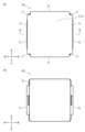
- FIG. 3A and 3B are top views of the inductor according to the first embodiment.
- the brazing material is omitted.
- the conductive shield is omitted.
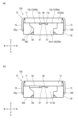
- 4(a) and 4(b) are front views of the inductor according to the first embodiment, in which the brazing material is omitted.
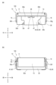
- 5A and 5B are rear and right side views of the inductor according to the first embodiment.
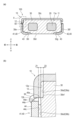
- FIG. 6(a) is a longitudinal sectional view of the inductor according to the first embodiment taken along the dashed line in Fig. 3(a) and seen in the direction of the arrows VI-VI.
- Fig. 6(b) is an enlarged view of the portion X shown by the dotted line in Fig. 6(a).
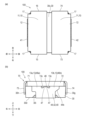
- FIG. 11 is a front view of an inductor according to a second embodiment.
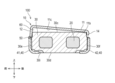
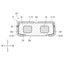
- FIG. 11 is a longitudinal sectional view of an inductor according to a third embodiment.
- FIG. 13 is a perspective view of an inductor according to a fourth embodiment.
- 10 is a longitudinal sectional view of the inductor according to the fourth embodiment taken along the dashed dotted line shown in FIG. 9 and seen in the direction of the arrows XX.
- 11A and 11B are top and rear views of the inductor according to the fourth embodiment.
- the various components of the inductor of the present invention do not need to be independent entities, and it is acceptable for multiple components to be formed as a single member, for one component to be formed from multiple members, for one component to be part of another component, or for part of one component to overlap with part of another component, etc.
- the front, back, left, right, top and bottom directions are defined as shown in the drawings. However, this is defined for the sake of convenience in order to easily explain the relative relationships between components, and does not limit the directions when manufacturing or using a product embodying the present invention.
- the center side of the inductor is sometimes called the inside and the opposite side the outside, and the direction from the surface of the inductor toward the center is sometimes called the inward direction and the opposite direction the outward direction.
- the term "flat surface” as used herein means a shape that is physically formed with a flat surface as a goal, and it is not necessarily required that the surface be a geometrically perfect flat surface.
- FIG. 1 is a perspective view showing an example of an inductor according to a first embodiment of the present invention.
- the inductor 100 includes a coil 20, a core 30 containing the coil 20, a pair of terminals 40 electrically connected to the coil 20, and a conductive shield 10 covering the surface of the core 30.
- the conductive shield 10 covers at least a portion of the upper or side surface of the core 30.
- the conductive shield 10 and one of the pair of terminals 40 (front terminal 41) are directly electrically connected.
- the conductive shield 10 and the other terminal (rear terminal 42) are indirectly electrically connected via the coil 20.
- the coil 20 is formed by winding a wire (coil wire, etc.) made of a conductive material such as metal.
- the part of the coil 20 around which the wire is wound is sometimes referred to as a winding portion 21.
- the wire may have a circular cross section or a flat cross section (e.g., an ellipse or a horizontally long rectangle).
- the winding axis direction of the coil 20 is the up-down direction, but is not limited to this.
- the winding axis direction of the coil 20 may be the left-right direction, the front-back direction, etc. As shown in FIG.
- the coil 20 is enclosed in the core 30.
- enclosed means that substantially the entire coil 20 is disposed inside the envelope volume of the core 30. A part of the coil 20 may not be covered by the core 30 and may be visible from the outside.
- the lead-out portion 22 (a portion drawn out from the winding portion 21), which is one end of the wire of the coil 20, may be disposed outside the core 30.
- the entire winding portion 21 of the coil 20, or the entire coil 20 including the winding portion 21 and the lead-out portion 22 both ends of the coil wire, etc. is covered by the core 30.
- the core 30 is a magnetic member that surrounds the coil 20.
- Examples of the magnetic material that forms the core 30 include ferrite.
- the core 30 also extends radially inside the coil 20, forming a closed loop as a whole.
- the core 30 in this embodiment is integrally formed by placing the coil 20 and the terminal 40 in a mold and pouring a resin containing a magnetic material such as ferrite into the mold. That is, the inductor 100 in this embodiment is a molded coil.
- the core 30 may be divided into a plurality of pieces, as will be described later in a modified example.
- the core 30 of this embodiment has a generally rectangular parallelepiped shape. As shown in Fig. 4(a) or 6(a), the core 30 has an upper surface 30c facing upward, a lower surface 30d facing downward, a front surface 30e facing forward, a rear surface 30f facing backward, a left surface 30g facing left, and a right surface 30h facing right.
- the areas of the upper surface 30c and the lower surface 30d of the core 30 are larger than the areas of the front surface 30e, the rear surface 30f, the left surface 30g, and the right surface 30h, respectively, and the core 30 has a generally flat shape.
- the shape of the core 30 is not limited to a rectangular parallelepiped, and may be, for example, a cylinder or a prism with a polygonal base.
- the surfaces constituting the core 30 do not need to be completely flat, and may be curved or distorted.
- the front surface 30e and the rear surface 30f of the core 30 are formed in a step-like shape. That is, for example, the front surface 30e (see Fig.
- FIG. 6(a) includes a concave surface 30e2 formed on the inside in the front-rear direction, a step surface 30e1 facing upward, and a convex surface 30e3 formed on the outside in the front-rear direction, as shown in Fig. 6(b).
- the rear surface 30f also includes a concave surface, a step surface, and a convex surface.
- the concave surface 30e2 is slightly inclined outward in the front-rear direction toward the bottom
- the convex surface 30e3 is slightly inclined inward in the front-rear direction toward the bottom.
- the inductor 100 has a pair of terminals 40, a front terminal 41 and a rear terminal 42.
- the inductor 100 has a pair of terminals 40, which means that the inductor 100 has at least a pair of terminals 40 connected to both ends of the coil wire.
- the inductor 100 may have terminals other than the pair of terminals.
- the front terminal 41 and the rear terminal 42 are conductive with one end and the other end of the coil 20, respectively. Specifically, as shown in FIG. 2, the end of the terminal 40 inserted into the core 30 (connection branch 46a described later) is bent into a U-shape and holds one end or the other end of the coil 20, sandwiching one end of the coil 20 in the vertical direction.
- the one end of the coil 20 and the terminal 40 are joined by a method such as laser welding or resistance welding.
- the mode of conduction between the coil 20 and the terminal 40 is not limited to this direct contact.
- the coil 20 and the terminal 40 may be conductive through a separate member.
- one end of the wire forming the coil may be wound around a winding terminal that is a separate member from the terminal 40, and the winding terminal may be connected to the terminal 40, so that the coil 20 and the terminal 40 are electrically connected via the winding terminal.
- the coil 20 and the terminal 40 may be integrally formed from the same member.
- the terminal 40 includes a mounting portion 43 joined to a mounting board (not shown), an outer surface arrangement portion 44 extending to a side surface of the core 30 (the front surface 30e or the rear surface 30f in this embodiment), and an insertion portion 45 inserted into the core 30.
- the upper end of the terminal 40 is the insertion portion 45
- the lower end is the mounting portion 43
- a portion between the insertion portion 45 and the mounting portion 43 is the outer surface arrangement portion 44.
- An inserted portion 45 at the upper end of the terminal 40 is inserted into the core 30.
- a terminal upper surface 45a of the inserted portion 45 and a stepped surface 30e1 on the front surface 30e of the core 30 are flush with each other.
- the terminal 40 protrudes forward or backward from the side surface (front surface 30e or rear surface 30f) of the core 30. That is, in this embodiment, the front-rear direction is the protruding direction of the terminal 40.
- the portion of the terminal 40 protruding outward from the core 30 is bent with respect to the insertion portion 45, and the part protruding from the core 30 (outer surface arrangement portion 44) is arranged along the front surface 30e or rear surface 30f of the core 30. Further, the terminal 40 is bent between the mounting portion 43 and the outer surface arrangement portion 44.
- the mounting portion 43 which is the lower end portion of the terminal 40, is approximately parallel to the lower surface 30d of the core 30. As shown in Fig.
- a part of the mounting portion 43 is arranged inside the terminal arrangement portion 30i formed by being recessed upward in the lower surface 30d of the core 30.
- the lower surface of the mounting portion 43 is arranged below the lower surface 30d of the core 30 so that the mounting portion 43 protrudes from the lower surface 30d of the core 30.
- the upper end of the terminal 40 branches out as described below to form two or more branches 46 (connecting branch 46a and non-contact branch 46b).
- a convex portion 48 formed in an upward convex shape is provided between the connecting branch 46a and the non-contact branch 46b at the base end of the branch 46.
- the convex portion 48 protrudes along the side surface of the core 30 without being bent like the branch 46.
- a downwardly recessed recess 47 is formed between the convex portion 48 and the connecting branch 46a, and between the convex portion 48 and the non-contact branch 46b.
- the outer surface arrangement portion 44 has a wide portion at the top and a narrower portion at the bottom, so that the outer surface arrangement portion 44 has an overall T-shape.
- a portion of the wide portion that connects to a non-contact branch portion 46b (described later) is chamfered to form a slope 44b, while a portion that connects to a connecting branch portion 46a is not chamfered and has a corner.
- the width of the outer surface arrangement portion 44 (the width of the narrow portion of the outer surface arrangement portion 44) is preferably one-third or more, or one-half or more, of the lateral width of the second surface or the third surface of the core 30, which will be described later.
- the outer surface arrangement portion 44 Since the outer surface arrangement portion 44 has a large width and widely covers the second surface or the third surface, leakage magnetic flux is blocked by the outer surface arrangement portion 44.
- the inductor 100 is grounded to the mounting board so that the mounting portion 43 is in contact with the mounting board.
- the mounting portion 43 and the mounting board are joined by soldering or the like and electrically connected.
- the terminals are terminals for surface mounting, with a flat mounting portion, but are not limited to this.
- the terminals 40 may be terminals with a mounting portion 43 in the shape of a pin.
- the conductive shield 10 is made of a conductive thin plate.
- An example of the conductive material is a metal such as copper.
- the conductive shield 10 covers a portion of each of the top surface 30c, the left surface 30g, the right surface 30h, the front surface 30e, and the rear surface 30f of the core 30, as described later.
- the conductive shield 10 may cover only a portion of the top surface or only a portion of the side surface.
- the conductive shield 10 may cover the entire surface of the core 30, as described later in a modified example. More specifically, the conductive shield 10 is formed by bending a thin metal plate as shown in Fig. 1, and covers the top and side surfaces of the core 30.
- the thin metal plate is formed into an X-shape, and the central part of the X-shape (a cover part 11 described later) covers almost the entire top surface 30c of the core 30 as shown in Fig. 3(a).
- a part of the conductive shield 10 extending forward from the top surface 30c of the core 30 (a front lip part 12 described later) is bent near the boundary between the top surface 30c and the front surface 30e of the core 30, and covers the front surface 30e of the core 30.
- the length of the front lip part 12 (the dimension extending downward from the top surface 30c of the core 30) is preferably equal to or greater than the distance from the top surface 30c of the core 30 to the terminal top surface 45a of the front terminal 41. In other words, it is preferable that the length of the front lip portion 12 is equal to or greater than the distance to the step surface 30e1 of the front surface 30e based on the top surface 30c of the core 30. In this embodiment, the length of the front lip portion 12 is equal to the distance to the terminal top surface 45a of the front terminal 41 based on the top surface 30c of the core 30, and is also equal to the distance to the step surface 30e1 based on the top surface 30c of the core 30. As shown in Fig.
- the portion of the conductive shield 10 that extends rearward beyond the upper surface 30c of the core 30 and is bent covers a part of the back surface 30f of the core 30.
- the length of the rear lip portion 14 is preferably shorter than the distance from the upper surface 30c of the core 30 to the terminal upper surface 45a of the front terminal 41.
- the portion of the conductive shield 10 that extends rightward or leftward beyond the upper surface 30c and is bent covers the right surface 30h or left surface 30g of the core 30.
- the length of the right lip portion 15 and the left lip portion 16 is preferably half or more, more preferably two-thirds or more, of the thickness of the core 30.
- Fig. 5(b) shows a right side view of the inductor 100, but the right side of the inductor 100 is mirror-symmetrical to the left side.
- the conductive shield 10 may not have lip portions (front lip portion 12, rear lip portion 14, right lip portion 15, and left lip portion 16) and may only include a cover portion 11 that covers the upper surface 30c (a first surface described later). Also, the conductive shield 10 may not cover all four side surfaces, and only some of the side surfaces may be covered by lip portions.
- notches 17 are provided between the front lip 12, the rear lip 14, the right lip 15 and the left lip 16, and these lips protrude independently from the cover portion 11.
- the provision of the notches 17 allows the conductive shield 10 to flexibly deform and cover the core 30.
- the cutouts 17 may not be provided, and the portions of the conductive shield 10 covering the respective side surfaces may be connected together in a continuous manner.
- direct electrical continuity between the conductive shield 10 and the front terminal 41 means that electrical continuity between the conductive shield 10 and the front terminal 41 does not pass through the coil 20.
- the conductive shield 10 (front lip portion 12) and the terminal 40 are in contact with each other, and the conductive shield 10 and the terminal 40 are directly electrically connected, but this is not limited to the above.
- the conductive shield 10 and the front terminal 41 may be electrically connected through a member other than the coil 20.
- the conductive shield 10 may not have a front lip portion 12, and the cover portion 11 of the conductive shield 10 and the terminal 40 may be electrically connected through a conductor.
- the conductive shield 10 and the rear terminal 42 being indirectly conductive means that they are conductive via the coil 20.
- the conductive shield 10 and the rear terminal 42 are conductive via the front terminal 41 and the coil 20. If the conductive shield 10 and the rear terminal 42 were conductive via a path that does not pass through the coil 20, the front terminal 41 and the rear terminal 42 would be conductive via two paths, one including the conductive shield 10 and the other including the coil 20, resulting in a short circuit. In contrast, in this embodiment, the conductive shield 10 and the rear terminal 42 are not in contact with each other as shown in FIG. 5A, and therefore no short circuit occurs.
- the core 30 has a first surface to which the end surface of the coil 20 (winding portion 21) faces.
- the end surface of the coil 20 faces up or down, and the first surface is the upper surface 30c or the lower surface 30d of the core 30.
- the first surface in this embodiment is the upper surface 30c of the core 30.
- the first surface is the front surface 30e or the back surface 30f, or the left surface 30g or the right surface 30h.
- the conductive shield 10 has a cover portion 11 that covers at least a part of the first surface (top surface 30c). In this embodiment, as shown in FIG.
- the cover portion 11 covers almost the entire top surface 30c, but since the cover portion 11 has a cutout portion 17, each corner of the rectangular top surface 30c is locally exposed from the cover portion 11 in a plan view.
- the cover portion 11 may cover the entire top surface 30c, or the cover portion 11 may cover a part of the top surface 30c that has a smaller shape and size. It is preferable that the end face of the coil 20 and the cover portion 11 overlap when viewed from the winding axis direction of the coil (the vertical direction in this embodiment). Furthermore, it is more preferable that the end face of the coil 20 is covered by the cover portion 11 when viewed from the winding axis direction of the coil.
- the core 30 has a second surface along which one terminal (front terminal 41) extends.
- the second surface is a part of the side surface.
- the surface of the core 30 along which the terminal 40 extends is, more specifically, the surface along which the outer surface arrangement portion 44 of the terminal 40 extends.
- the outer surface arrangement portion 44 of the front terminal 41 is arranged along the front surface 30e of the core 30.
- the second surface is the front surface 30e of the core 30.
- the second surface may be another surface of the side surface (the right surface 30h, the left surface 30g, or the back surface 30f).
- a portion of the conductive shield 10 covers a portion of the second surface (front surface 30e).
- the front lip portion 12 covers substantially the entirety of the front surface 30e of the core 30 that is located above the terminal upper surface 45a (see Fig. 6(b)) of the front terminal 41.
- the front lip portion 12 may extend below the terminal upper surface 45a of the front terminal 41 to cover the underside of the front surface 30e of the core 30.
- the conductive shield 10 (front lip portion 12) covering the second surface (front surface 30e) is in contact with one terminal (front terminal 41).
- the upper surface (terminal upper surface 45a) of the front terminal 41 is in surface contact with the end surface 12b of the front lip portion 12.
- the front terminal 41 and the front lip portion 12 may be in substantial line contact. Also, the front terminal 41 and the front lip portion 12 may be in point contact.
- the conductive shield 10 cover a portion of the second surface (front surface 30e), magnetic flux leaking from the core 30 can be blocked more effectively.
- the inner surface (lip inner surface 12a) of a portion (front lip portion 12) of the conductive shield 10 covering the second surface (front surface 30e) of the core 30 is disposed inward in a plan view from the inner surface (terminal inner surface 44c) that is aligned with the second surface of one terminal (front terminal 41). More precisely, the lip inner surface 12a is disposed inward in the protruding direction (front-rear direction) of the terminal 40 from the terminal inner surface 44c.
- the terminal inner surface 44c that is aligned with the front surface 30e of the front terminal 41 is the inner surface of the outer surface arrangement portion 44 of the front terminal 41.
- a plan view means being disposed toward the center of the inductor 100 when viewed from above.
- a plan view does not necessarily mean being able to be directly confirmed with the naked eye.
- the lip portion inner surface 12a is disposed on the inside in the front-rear direction of the terminal inner surface 44c of the front terminal 41 when viewed in a vertical cross section as shown in FIG. 6(b).
- the terminal 40 is bent between the insertion portion 45 and the outer surface arrangement portion 44, and the outer surface of the bent portion is a curved surface 44d.
- the lip portion inner surface 12a By arranging the lip portion inner surface 12a on the inside of the terminal inner surface 44c of the front terminal 41 in the terminal protruding direction, at least a part of the end surface 12b (including the sides of the rectangular end surface 12b) of the front lip portion 12 contacts the upper surface (terminal upper surface 45a) of the insertion portion 45 of the front terminal 41 as shown in Fig. 6(b).
- a part of the inner side of the end surface 12b of the front lip portion 12 in the terminal protruding direction contacts the horizontal terminal upper surface 45a of the insertion portion 45, and another part of the outer side of the end surface 12b in the terminal protruding direction faces the curved surface 44d at a distance.
- the entire end surface 12b of the front lip portion 12 may contact the terminal upper surface 45a of the insertion portion 45.
- the outer surface of the front lip portion 12 is preferably positioned more inward in the terminal protruding direction than the terminal inner surface 44c of the front terminal 41, or is preferably positioned on the same plane as the terminal inner surface 44c of the front terminal 41.
- the lip inner surface 12a of the front lip 12 and the terminal inner surface 44c of the front terminal 41 are offset from each other in the front-rear direction, and the front lip 12 and the front terminal 41 are in surface contact at the end surface 12b, thereby providing good electrical conduction between the front terminal 41 and the conductive shield.
- a part of the end surface 12b of the front lip 12 faces the curved surface 44d of the front terminal 41, forming a recess that is surrounded by the end surface 12b of the front lip 12 and the curved surface 44d of the front terminal 41 and narrows toward the inside in the terminal protrusion direction.
- Solder 50 which will be described later, enters the recess, thereby firmly connecting the conductive shield 10 and the front terminal 41.
- the distance between the lip inner surface 12a and the terminal inner surface 44c of the front terminal 41 is preferably at least one-quarter of the thickness (dimension in the front-to-rear direction) of the front lip portion 12, or at least half of that thickness.
- the thickness of the front lip portion 12 is, in other words, the front-to-rear width of the end face 12b of the front lip portion 12.
- the maximum value of distance Z1 is equal to or smaller than the thickness of the front lip portion 12.
- the distance between the lip inner surface 12a and the terminal inner surface 44c is the distance in the terminal protruding direction between the lower end of the lip inner surface 12a and the upper end of the terminal inner surface 44c.
- the lip portion inner surface 12a is disposed on the same plane as the upper end of the convex surface 30e3 of the front surface 30e of the core 30.
- the conductive shield 10 may be in contact with a portion of the front terminal 41 other than the terminal inner surface 44c (such as the curved surface 44d).
- the lip inner surface 12a and the terminal inner surface 44c of the front terminal 41 may be disposed on the same plane, or the lip inner surface 12a of the front lip 12 may be disposed outward of the terminal inner surface 44c of the front terminal 41.
- the conductive shield 10 and the front terminal 41 are substantially in line contact or not in contact at all, it is preferable to sufficiently ensure electrical continuity between the conductive shield 10 and the front terminal 41 by brazing or the like.
- a portion (shield covering portion 30a) of the second surface (front surface 30e) of the core 30 that is covered by the conductive shield 10 is formed inward in a plan view from a portion (terminal covering portion 30b) of the second surface that is covered by one terminal.
- the shield covering portion 30a is a region of the front surface 30e of the core 30 that is covered by the conductive shield 10.
- substantially the entire portion except for a portion exposed from the cutout portion 17 is the shield covering portion 30a.
- the distance between the shield covering portion 30a and the terminal covering portion 30b is the distance between the lower end of the shield covering portion 30a and the upper end of the terminal covering portion 30b in the terminal protruding direction.
- the entire part (concave surface 30e2) above the step surface 30e1 of the front surface 30e of the core 30 is disposed inward in the terminal protruding direction from the entire part (convex surface 30e3) below the step surface 30e1 of the front surface 30e of the core 30.
- the shield covering portion 30a of the front surface 30e may be recessed backward, and the recessed shield covering portion 30a may be disposed inward in the terminal protruding direction from the terminal covering portion 30b.
- only the terminal covering portion 30b of the front surface 30e of the core 30 may protrude forward, and the protruding terminal covering portion 30b may be disposed outward in the terminal protruding direction from the shield covering portion 30a.
- the portion not covered by the front lip portion 12 may be disposed outward or inward from the terminal covering portion 30b in the terminal protruding direction. Due to the misalignment between the shield covering portion 30a and the terminal covering portion 30b on the second surface, the front lip portion 12 is more likely to be disposed inward in a plan view than the front terminal 41. In other words, the end face 12b of the front lip portion 12 is more likely to come into surface contact with the front terminal 41, making it easier to maintain good electrical continuity between the conductive shield 10 and the front terminal 41.
- the inner surface of the cover portion 11 (the cover portion inner surface 11 a ) is disposed substantially parallel to the upper surface 30 c of the core 30 .
- An insulating material may or may not be applied by coating or the like to a portion of the surface of the core 30 that is covered by the conductive shield 10 (part of the top and side surfaces) or to substantially the entire inner surface of the conductive shield 10.
- the cover portion inner surface 11a of the cover portion 11 and the top surface 30c of the core 30 are arranged along each other with the insulating material sandwiched therebetween.
- the conductive shield 10 and one terminal are joined by welding or brazing.
- welding include fusion welding using a laser or gas.
- brazing include soldering using solder or other metal brazing materials.
- the conductive shield 10 and the front terminal 41 are brazed with solder 50.
- the conductive shield 10 may be brazed or welded to both branches 46 of the front terminal 41, which will be described later, or may be brazed or welded to only one of the branches.
- the conductive shield 10 and the front terminal 41 do not have to be joined by brazing or welding.
- the conductive shield 10 and the front terminal 41 may be abutted against each other to ensure electrical continuity.
- the conductive shield 10 and the front terminal 41 may be fixed to each other by an adhesive.
- one terminal has two or more branches formed by branching one end.
- the front terminal 41 has two branches 46.
- the branches 46 are formed so as to protrude upward from the outer surface arrangement portion 44, in other words, the branches 46 are formed by branching the terminal 40 at the upper part of the outer surface arrangement portion 44. That is, in the front terminal 41, a connecting branch 46a (to be described later) is formed from the upper right of the outer surface arrangement portion 44, and a non-contact branch 46b (to be described later) is formed from the upper left of the outer surface arrangement portion 44.
- the branch 46 is not limited to such a shape, and for example, the branch 46 may be formed by branching from the middle of the outer surface arrangement portion 44, or may be formed by branching from the middle of the insertion portion 45.
- the base end (the root part where the terminal 40 branches) of the branch 46 is located outside the core 30 as in this embodiment. 2 , a portion of each of the branches 46 is inserted into the core 30.
- substantially the entirety of the branch 46 is inserted into the core 30, and a portion of the base end side of the branch 46 is disposed outside the core 30.
- the branch 46 is the same as the inserted portion 45.
- the other terminal (rear terminal 42), like the front terminal 41, is branched to form a branch portion 46, and a part of the branch portion 46 is inserted into the core 30.
- the front terminal 41 and the rear terminal 42 have shapes that are mirror images of each other.
- connection branch 46a is directly conductive with the coil 20
- non-contact branch 46b is indirectly conductive with the coil 20 via the one branch (connection branch 46a).
- the indirect conductive connection between the non-contact branch 46b and the coil 20 means that the non-contact branch 46b is conductive via the connection branch 46a. In other words, the entire non-contact branch 46b is not in contact with the coil 20.
- the non-contact branch 46b and the coil 20 are conductive via the connection branch 46a and the outer surface arrangement portion 44.
- the non-contact branch 46b and the conductive shield 10 are soldered with solder 50.
- the solder 50 penetrates into the gap between the front terminal 41 and the conductive shield 10, and is also disposed, for example, between the end surface 12b of the front lip portion 12 and the curved surface 44d of the front terminal 41 as shown in Fig. 6(b).
- the connection branch 46a is in contact with the conductive shield 10, but it does not have to be in contact. It is preferable that the connection branch 46a and the conductive shield 10 are not joined.
- the solder 50 is not disposed between the contact portions 13, 13 described below, but it may be disposed therebetween.
- the connecting branch 46a By joining the non-contact branch 46b, which is not directly conductive with the coil 20, to the conductive shield 10 in this manner, it is not necessary to join the connecting branch 46a, which is directly conductive with the coil 20, to the conductive shield 10. This makes it possible to minimize the thermal load on the connecting branch 46a.
- the connecting branch 46a and the conductive shield 10 may be joined, and the non-contact branch 46b and the conductive shield 10 may not be joined.
- Second Embodiment differs from the first embodiment only in the manner in which the conductive shield 10 and the front terminal 41 are joined; the conductive shield 10, coil 20, core 30 and terminal 40 of the inductor 100 in this embodiment are common to the first embodiment.
- the conductive shield 10 and one terminal (front terminal 41) are joined by welding or brazing.
- one terminal has two or more branches 46 formed by branching one end, and a portion of each of the branches 46 is inserted into the core 30.
- each of the two or more branches 46 (the connection branch 46a and the non-contact branch 46b shown in Fig. 4(a)) is joined to the conductive shield 10.
- the solder 50 joining the connection branch 46a to the conductive shield 10 and the solder 50 joining the non-contact branch 46b to the conductive shield 10 may be continuous or divided, as described below. In this manner, each of the two or more branches 46 is joined to the conductive shield 10, thereby firmly connecting the front terminal 41 and the conductive shield 10.
- one terminal contacts the conductive shield 10 at each of two or more contact portions 13 spaced apart from each other, as in the first embodiment shown in Fig. 4(a).
- the connection branch portion 46a contacts the conductive shield 10
- the non-contact branch portion 46b contacts the conductive shield 10.
- the contact portion 13 refers to the portion of the front terminal 41 that contacts the conductive shield 10 and a portion of its vicinity, and in this embodiment refers to a portion of the terminal upper surface 45a of the front terminal 41 and its vicinity.
- the contact portion 13 in this embodiment is a portion of the base end side of the branch portion 46 (the front end portion of the inserted portion 45 and the bent portion between the inserted portion 45 and the outer surface disposed portion 44).
- a brazing material solder 50
- a part of the solder 50 is disposed between the opposing end faces 13c, 13c (see FIG. 4(a)) of the contact portions 13 facing each other.
- a recess surrounded by one contact portion 13a, the upper end face 44a (see FIG. 2 or FIG.
- solder 50 enters and accumulates in the recess as shown in FIG. 7. More specifically, the solder 50 is in contact with each of the upper end face 44a (see FIG. 6(b)) of the front terminal 41, the end face 12b of the front lip portion 12, and the opposing end face 13c (see FIG. 4(a)) of the contact portion 13. In this embodiment, as shown in Fig. 4(a) and Fig. 7, the solder 50 joins the upper end surface 44a (see Fig. 6(b)) of the front terminal 41 to the end surface 12b of the front lip portion 12.
- first contact portion 13a, the second contact portion 13b, and the area between the first contact portion 13a and the second contact portion 13b of the first terminal (front terminal 41) are all joined to the conductive shield 10 by the brazing material (solder 50). Also, the solder 50 joining the first contact portion 13a, the second contact portion 13b, and the area between the first contact portion 13a and the second contact portion 13b of the first terminal (front terminal 41) to the conductive shield 10 is arranged in a continuous manner.
- the solder 50 By arranging the solder 50 between the contact portions 13, 13, the solder 50 can accumulate on the upper end surface 44a of the front terminal 41, particularly within the recess 47, thereby preventing the liquid solder 50 from flowing off when the front terminal 41 and the conductive shield 10 are soldered together.
- the solder 50 contacts not only the curved surface 44d of the front terminal 41 but also the upper end surface 44a on which the recessed portion 47 and the protruding portion 48 are formed, so that the solder 50 contacts the front terminal 41 in various directions. This prevents the solder 50 from peeling off from the front terminal 41.
- the cross section of the solder 50 disposed between the contact portions 13a, 13b (a cross section perpendicular to the extending direction of the solder, i.e., the left-right direction) has a larger dimension and a different shape than the cross section of the solder 50 disposed on the upper edge of the contact portion 13. That is, the thickness (dimension in the front-to-rear direction) of the solder 50 disposed between the contact portions 13a, 13b is larger than the thickness of the solder 50 disposed in the vicinity of the contact portion 13. For this reason, even when subjected to thermal load over time, the solder 50 disposed between the contact portions 13a, 13b is less likely to crack, and the bond between the conductive shield 10 and the terminal 40 can be maintained.
- Fig. 8 differs from the first or second embodiment only in the manner in which the conductive shield 10 is placed.
- the conductive shield 10, coil 20, core 30, terminal 40, and solder 50 of the inductor 100 in this embodiment are common to the inductor 100 in the first or second embodiment, and the shape as viewed from above is generally common to the inductor 100 of the first embodiment shown in Fig. 3(a).
- Fig. 8 is a vertical cross-sectional view of the inductor 100 of the third embodiment. The position and viewing direction of the vertical cross-section shown in Fig. 8 are common to the arrow VI-VI shown in Fig. 3(a) according to the first embodiment.
- a part of the cover part 11 (core contact part 11b) and the core 30 are in contact with each other, and a hollow part 60 is provided between another part of the cover part 11 (separation part 11c) and a part of the first surface (upper surface 30c).
- the length of the front lip part 12 is greater than the distance to the terminal upper surface 45a of the front terminal 41 based on the upper surface 30c of the core 30. Therefore, as a result of the front lip part 12 and the front terminal 41 being in contact with each other, a part of the second surface side of the cover part inner surface 11a (see FIG. 6(a)) is separated from a part of the upper surface 30c of the core 30.
- one end of the end surface 12b of the front lip part 12 on the inside in the terminal protruding direction (for example, an inner side in the terminal protruding direction of the rectangular end surface 12b) is in contact with the front terminal 41.
- the front lip part 12 is in contact with the terminal upper surface 45a or the curved surface 44d of the front terminal 41.
- the height of the hollow portion 60 is exaggerated.
- the maximum height of the hollow portion 60 (the dimension from the top surface 30c of the core 30 to the highest point of the hollow portion 60) is preferably smaller than the plate thickness of the conductive shield 10 (cover portion 11).
- the core contact portion 11b that contacts the core 30 is a part of the rear side of the cover portion 11, and the separation portion 11c is a part of the cover portion 11 that is further forward (on the second surface side) than the core contact portion 11b.
- the core contact portion 11b contacts a corner that is a boundary between the upper surface 30c and the rear surface 30f of the core 30.
- the conductive shield 10 is in contact with the lower end of the inner surface of the rear lip portion 14 and part of the lip portion inner surface 12a (see FIG. 6(b)) of the front lip portion 12.
- the lower end of the inner surface of the rear lip portion 14 is in contact with the back surface 30f of the core 30, and the lip portion inner surface 12a (see FIG. 6(b)) of the front lip portion 12 is in contact with a corner that forms the boundary between the top surface 30c and the front surface 30e of the core 30.
- the hollow portion 60 is a space defined by the separation portion 11 c , the lip portion inner surface 12 a of the front lip portion 12 , the first surface (upper surface 30 c ), and the inner surfaces of the right lip portion 15 and the left lip portion 16 .
- the hollow portion 60 may be provided without the cover portion inner surface 11a being in contact with the core 30.
- the cover portion inner surface 11a may not be in contact with a corner of the boundary between the upper surface 30c and the rear surface 30f of the core 30, and the lower end of the rear lip portion 14 may be in contact with the core 30. Because there is a hollow portion 60 between the core 30 and the cover portion 11, the core 30 and the cover portion 11 can be insulated by the air in the hollow portion 60 without having to apply insulating material to the surface of the core 30 covered by the cover portion 11 or to the inner surface 11a of the cover portion.
- the cover portion 11 is inclined downward from the other portion (separation portion 11c) toward the other portion (core contact portion 11b) so as to approach the first surface (upper surface 30c).
- the downward inclination does not necessarily mean a downward inclination in the actual up-down relationship, but means an inclination approaching the first surface when the first surface is used as a reference.
- the cover portion 11 intersects with the first surface.
- the thickness (dimension in the up-down direction) of the hollow portion 60 gradually increases toward the second surface (front surface 30e) and gradually decreases toward the back surface 30f of the core 30.
- the front lip portion 12 and the front terminal 41 can be reliably abutted against each other.
- this embodiment differs from the first, second or third embodiment in that it has not only the conductive shield 10 but also a second conductive shield 70.
- the coil 20, core 30, terminals 40 and solder 50 in the inductor 100 of this embodiment are common to the first, second or third embodiment.
- the inductor 100 of this embodiment has a second conductive shield (second conductive shield 70).
- the second conductive shield 70 covers at least a part of the top or side surface of the core.
- the second conductive shield 70 and the other terminal (rear terminal 42) are in direct electrical continuity, and the second conductive shield 70 and the one terminal (front terminal 41) are indirectly electrical continuity via the coil 20.
- Direct electrical continuity between the second conductive shield 70 and the rear terminal 42 means that the second conductive shield 70 and the rear terminal 42 are electrical continuity via a path that does not go through the coil 20.
- the second conductive shield 70 and the rear terminal 42 may also be electrical continuity via a member other than the coil 20 (e.g., a conductor, etc.).
- the second conductive shield 70 has a rear lip portion 72 that covers a portion of the third surface (the rear surface 30f of the core 30 in this embodiment) to which the outer surface arrangement portion 44 of the rear terminal 42 extends, a right lip portion 73 that covers the right surface 30h of the core 30, and a left lip portion 74 that covers the left surface 30g of the core 30.
- the rear lip portion 72 of the second conductor shield 70 contacts the rear terminal 42. Similar to the front lip portion 12 of the conductor shield 10, the rear lip portion 72 contacts the rear terminal 42 at a surface of the lower end surface.
- the contact portion between the rear lip portion 72 and the rear terminal 42 may be substantially a line or may be a point.
- the conductive shield 10 and the second conductive shield 70 cover only a portion of the first surface (the upper surface 30c of the core 30). Specifically, the conductive shield 10 covers the front half of the upper surface 30c, but does not cover the rear half of the upper surface 30c. Also, the second conductive shield 70 covers the rear half of the upper surface 30c, but does not cover the front half. More specifically, the conductive shield 10 and the second conductive shield 70 have the same shape and dimensions, and the areas of the upper surface 30c covered by the conductive shield 10 and the second conductive shield 70 are approximately equal.
- the dimensions of the cover portion 11 of the conductive shield 10 and the dimensions of the second cover portion 71 covering the first surface of the second conductive shield 70 may be larger or smaller, respectively.
- Either the conductive shield 10 or the second conductive shield 70 may cover the center of the upper surface 30c, and either the conductive shield 10 or the second conductive shield 70 may overlap an end face of the coil 20 when viewed from the winding axis direction of the coil 20.
- the front side of the upper surface 30c of the core 30 is covered by the conductive shield 10
- the rear side is covered by the second conductive shield 70.
- this is not limited to this.
- the right side of the upper surface 30c of the core 30 may be covered by the conductive shield 10
- the left side may be covered by the second conductive shield 70.
- the second cover part 71 and the first surface (top surface 30c) are substantially parallel, and substantially the entire inner surface of the second cover part 71 is in contact with the top surface 30c.
- a part of the second cover part 71 may be in contact with the core 30, and a hollow part may be provided between another part of the second cover part 71 and a part of the top surface 30c.
- a hollow part is provided, one end on the front side of the second cover part 71 is in contact with the top surface 30c of the core 30, and the second cover part 71 is inclined downward with respect to the first surface (top surface 30c) from one end on the third surface (back surface 30f) side to the other end on the second surface (front surface 30e) side.
- substantially the entire cover portion 11 of the conductive shield 10 contacts the front half of the upper surface 30c of the core 30. If a hollow portion is provided between the conductive shield 10 and the core 30, one end of the rear side of the conductive shield 10 contacts the upper surface 30c of the core 30.
- the second conductive shield 70 and the rear terminal 42 are joined by welding or brazing.
- the manner of joining is similar to the joining between the conductive shield 10 and the front terminal 41, in that the rear terminal 42 has two or more branches 46, and each of the two or more branches 46 may be joined to the second conductive shield 70, or only one branch 46 may be joined to the conductive shield 10.
- the inner surface of the rear lip portion 72 covering the rear surface 30f which is the third surface, is located more inward in a plan view than the inner surface of the rear terminal 42 that is along the rear surface 30f. Also, it is preferable that the part of the third surface that is covered by the second conductive shield 70 is formed more inward in a plan view than the other part of the third surface that is covered by the rear terminal 42. This allows the second conductive shield 70 and the rear terminal 42 to come into surface contact and provide good electrical conductivity.
- the conductive shield 10 and the second conductive shield 70 are spaced apart from each other. A sufficient creepage distance is maintained so that the conductive shield 10 and the second conductive shield 70 are not directly conductive to each other.
- the rear-facing end face of the conductive shield 10 and the forward-facing end face of the second conductive shield 70 face each other at a distance.
- the conductive shield 10 and the second conductive shield 70 are arranged so that their end faces face each other and are aligned, and the distance between the conductive shield 10 and the second conductive shield 70 is approximately uniform.
- the length of the rear lip portion 72 can be made longer than in the first, second, and third embodiments. This allows leakage magnetic flux to be blocked over a wider area of the back surface 30f of the core 30.
- the conductive shield 10 covers a portion of the surface of the core 30, but this is not limited thereto, and the conductive shield 10 may cover the entire surface of the core 30.
- the conductive shield 10 may be a rectangular parallelepiped having a cavity capable of containing the entire core 30, with only the mounting portion 43 exposed to the outside of the conductive shield 10. In this case, a sufficient creepage distance is maintained between the conductive shield 10 and the rear terminal 42 so that they are not directly conductive without passing through the coil 20.
- the front lip portion 12 and the front terminal 41 do not have to be in contact. In that case, the front lip portion 12 and the front terminal 41 are electrically connected via a separate member.
- the front lip portion 12 and the front terminal 41 are joined by solder 50, and the front lip portion 12 and the front terminal 41 are electrically connected via the solder 50.
- the terminal 40 having the branch portion 46 is exemplified, but this is not limited to the above.
- the terminal 40 may not have the branch portion 46 and may be in contact with the conductive shield 10 at one contact portion 13.
- the front terminal 41 may be joined to the conductive shield 10 at the entire contact portion 13, or the front terminal 41 may be joined to the conductive shield 10 at one part of the contact portion 13 and not joined to the conductive shield 10 at another part of the contact portion 13.
- the core 30 is integrally formed, but this is not limiting, and the core 30 may be composed of multiple parts.
- the core 30 may be divided into an upper core and a lower core by a stepped surface 30e1 (see FIG. 6(b)) provided on the core 30 described later.
- the core 30 may be a pot core.
- the core 30 may be formed by combining a core that covers the circumferential surface and one end face of the coil 20, a columnar core that is inserted through the center of the coil 20, and a plate-shaped core that covers the other end face of the coil 20. In this case, for example, it is recommended to arrange the conductive shield 10 so as to cover the upper side of the plate-shaped core.
- An inductor having a coil, a core containing the coil, a pair of terminals electrically connected to the coil, and a conductive shield covering a surface of the core, the conductive shield covers at least a portion of a top surface or a side surface of the core; the conductive shield and one of the pair of terminals are directly conductive to each other, An inductor, wherein the conductive shield and another terminal are indirectly conductive with each other via the coil.
- the core has a first surface to which an end surface of the coil faces, The inductor according to (1), wherein the conductive shield has a cover portion that covers at least a portion of the first surface.
- the core has a second surface from which the one terminal extends, a portion of the conductive shield covering a portion of the second surface;
- a part of the cover portion is in contact with the core,
- the one terminal has two or more branch portions formed by branching one end portion, A portion of each of the branches is inserted into the core, One of the branches is in direct electrical communication with the coil, At least one of the other branches is indirectly conductive with the coil via the one branch, The inductor according to (8), wherein the other branch portion and the conductive shield are in contact with each other and joined together.
- the one terminal has two or more branch portions formed by branching one end portion, A portion of each of the branches is inserted into the core, The inductor according to (8), wherein each of the two or more branches is joined to the conductive shield.
- the one terminal is in contact with the conductive shield at two or more contact portions spaced apart from each other,
- the inductor of (10) wherein the brazing material is disposed between one of the contact portions and the other of the contact portions, and the one of the contact portions, the other of the contact portions, and the portion between the one of the contact portions and the other of the contact portions in the one of the terminals are all joined to the conductive shield by the brazing material.
- a second conductive shield is provided; the second conductive shield covers at least a portion of a top or side surface of the core; the second conductive shield and the other terminal are in direct electrical contact; the second conductive shield and the one terminal are indirectly conductive to each other via the coil,
- the inductor according to any one of (1) to (11), wherein the conductive shield and the second conductive shield are spaced apart from each other.
- An inductor wherein the length of the portion of the conductive shield that covers the second surface is equal to or greater than the distance to the one terminal based on the first surface.
- An inductor wherein at least a portion of an end surface of a portion of the conductive shield that covers the second surface comes into surface contact with the one terminal.
- conductive shield 11 cover portion 11a cover portion inner surface 11b core contact portion 11c separation portion 12 front lip portion 12a lip portion inner surface 12b end surface 13 contact portion 13a one contact portion 13b other contact portion 13c opposing end surface 14 rear lip portion 15 right lip portion 16 left lip portion 17 notch portion 20 coil 21 winding portion 22 lead-out portion 30 core 30a shield covering portion 30b terminal covering portion 30c upper surface 30d lower surface 30e front surface 30e1 step surface 30e2 concave surface 30e3 convex surface 30f rear surface 30g left surface 30h right surface 30i terminal arrangement portion 40 terminal 41 front terminal 42 rear terminal 43 mounting portion 44 outer surface arrangement portion 44a upper end surface 44b inclined surface 44c Terminal inner surface 44d, curved surface 45, inserted portion 45a, terminal upper surface 46, branch portion 46a, connecting branch portion 46b, non-contact branch portion 47, recess 48, protrusion 50, solder 60, hollow portion 70, second conductive shield 71, second cover portion 72, rear lip portion 73, right lip portion 74,
Landscapes
- Engineering & Computer Science (AREA)
- Power Engineering (AREA)
- Coils Or Transformers For Communication (AREA)
Abstract
Description
この種の技術に関し、下記特許文献1には、コイル(310)を取り囲むコア本体(115)、コイル(310)に電気的に連絡する端子(特許文献1におけるリード部(120))およびコア本体(115)の外面の少なくとも一部を被覆する導電体シールド(特許文献1における遮蔽装置(500))を有するインダクタが開示されている。
特許文献1においては、導電体シールドは半田パッド(900)に電気的に接続し、端子は導電体シールドが接続する半田パッド(900)とは異なる半田パッド(910)に電気的に接続して、インダクタは接地されている。
なお、本実施の形態では図示するように前後左右上下の方向を規定して説明する。しかし、これは構成要素の相対関係を簡単に説明するために便宜的に規定するものであり、本発明を実施する製品の製造時や使用時の方向を限定するものではない。また、インダクタの中心側を内側、その反対を外側と呼称し、インダクタの表面から中心に向かう向きを内向き、その反対向きを外向きと呼称することがある。
また、本発明でいう平面とは、平面を目標として物理的に形成した形状を意味しており、当然ながら幾何学的に完全な平面であることは要しない。
図1は、本発明の第一の実施形態にかかるインダクタの一例を示す斜視図である。
インダクタ100は、コイル20と、コイル20を内包するコア30と、コイル20と導通する二つで一対の端子40と、コア30の表面を覆う導電体シールド10と、を有する。導電体シールド10は、コア30の上面または側面の少なくとも一部を覆っている。導電体シールド10と一対の端子40のいずれか一の端子(前方端子41)とが直接に導通している。また、導電体シールド10と他の端子(後方端子42)とが、コイル20を介して間接に導通している。
コイル20は、図2に図示されるように金属等の導電性の材料で作られた線材(コイルワイヤ等)が巻回されたものである。コイル20において線材が巻回されている部分を特に巻回部21と呼ぶことがある。図2においては巻回される線材の各ターンについては図示を省略している。線材は断面が円形のものでも、断面が偏平なもの(例えば楕円や横長の矩形)でもよい。本実施形態では、コイル20の巻軸方向は上下方向であるが、これに限られない。コイル20の巻軸方向は左右方向や前後方向等であってもよい。
図1に図示されるように、コイル20はコア30に内包されている。ここで内包とは、コイル20の略全部がコア30の包絡体積の内部に配置されていることをいう。コイル20の一部がコア30に覆われておらず外部から視認できる状態でもよい。例えば、コイル20の線材の一端部である引出部22(巻回部21から引き出された部分)がコア30の外部に配置されていてもよい。好ましくは、コイル20の巻回部21の全部、または巻回部21および引出部22(コイルワイヤ等の両端部)を含めたコイル20の全部、がコア30に覆われている。
本実施形態に代えて、変形例にて後述するように、コア30が複数に分かれていてもよい。
コア30の形状は直方体に限られず、例えば円柱や底面が多角形の角柱でもよい。コア30を構成する面は完全な平面である必要はなく、湾曲していても、歪んでいてもよい。
本実施形態においては、図3(b)および図6(a)に図示されるように、コア30の前面30eおよび背面30fは一段の階段状に形成されている。すなわち、例えば前面30e(図6(a)参照)は、図6(b)に図示されるように前後方向の内側に形成された凹面30e2、上方を向く階段面30e1および前後方向の外側に形成された凸面30e3を含む。背面30fも同様に凹面、階段面および凸面を含む。
本実施形態に代えて、前面30eおよび背面30fは段差のないように形成されていてもよい。図6(b)に図示されるように、本実施形態において凹面30e2は下方ほど前後方向の外側に若干傾いており、凸面30e3は下方ほど前後方向の内側に若干傾いている。
端子40の上端部にあたる内挿部45はコア30に内挿されている。図6(b)に図示されるように内挿部45の端子上面45aと、コア30の前面30eにおける階段面30e1と、は面一になっている。
図6(a)に図示されるように、端子40はコア30の側面(前面30eまたは背面30f)から前方または後方に向けて突出している。すなわち、本実施形態において前後方向が端子40の突出方向である。図1および図2に図示されるように、端子40のうちコア30の外方に突出した部分は内挿部45に対して折り曲げられて、コア30から突出した一部(外面配置部44)はコア30の前面30eまたは背面30fに沿って配置されている。
また、実装部43と外面配置部44との間において端子40は折り曲げられている。端子40の下端部である実装部43は、コア30の下面30dと略平行に沿っている。図6(a)に図示されるように、実装部43の一部はコア30の下面30dに上向きに凹んで形成された端子配置部30iの内部に配置される。実装部43がコア30の下面30dよりも突出するように、実装部43の下面はコア30の下面30dよりも下側に配置されている。
外面配置部44の幅(外面配置部44のうち幅狭な部分の幅)は後述するコア30の第二の面または第三の面の横幅の三分の一以上、または半分以上であることが好ましい。外面配置部44の幅が大きく、外面配置部44によって第二の面または第三の面が広く覆われることにより、漏れ磁束が外面配置部44によって遮断される。
インダクタ100は実装部43が実装基板に接するように実装基板に接地される。実装部43と実装基板とは半田付けなどによって接合されて電気的に接続する。
本実施形態において端子は実装部が偏平である平面実装用の端子であるがこれに限られない。端子40は、実装部43がピン形状の端子でもよい。
より具体的には、導電体シールド10は、図1に図示されるように金属製薄板が折り曲げられており、コア30の上面および側面を覆っている。金属製薄板はX字形状に形成されて、図3(a)に図示されるようにX字形状の中央部分(後述するカバー部11)がコア30の上面30cの略全部を覆っている。図6(a)および図6(b)に図示されるように、導電体シールド10のうちコア30の上面30cから前方に延出した一部(後述する前方リップ部12)は、コア30の上面30cと前面30eとの境界の近傍で折り曲げられており、コア30の前面30eを覆っている。前方リップ部12の長さ(コア30の上面30cを基準として下方に向かう寸法)は、コア30の上面30cを基準とした前方端子41の端子上面45aまでの距離と同じか、それより大きいことが好ましい。換言すれば、前方リップ部12の長さはコア30の上面30cを基準とした前面30eの階段面30e1までの距離と同じかそれ以上であることが好ましい。本実施形態においては、前方リップ部12の長さは、コア30の上面30cを基準とした前方端子41の端子上面45aまでの距離と等しく、またコア30の上面30cを基準とした階段面30e1までの距離と等しい。
図5(b)に図示されるように導電体シールド10においてコア30の上面30cよりも後方に延出して折り曲げられた部分(後方リップ部14)は、コア30の背面30fの一部を覆っている。後方リップ部14の長さはコア30の上面30cを基準とした前方端子41の端子上面45aまでの距離よりも小さいことが好ましい。図4(a)および図5(b)に図示されるように、上面30cよりも右方または左方に延在して折り曲げられた導電体シールド10の一部(右方リップ部15または左方リップ部16)はコア30の右面30hまたは左面30gを覆っている。右方リップ部15および左方リップ部16の長さは、コア30の厚さの好ましくは半分以上、より好ましくは三分の二以上である。図5(b)においては、インダクタ100の右面図を示しているが、インダクタ100の右面は左面と鏡面対称である。
導電体シールド10がコア30の上面30cの他に側面(前面30e、背面30f、右面30hまたは左面30g)を覆うことで、側面から漏れる磁束を遮蔽できる他、導電体シールド10の位置ずれを防止できる。
本実施形態に代えて、導電体シールド10はリップ部(前方リップ部12、後方リップ部14、右方リップ部15および左方リップ部16)を有さず、上面30c(後述する第一の面)を覆うカバー部11のみを含んでもよい。また、導電体シールド10は側面である四面のすべてを覆わず、一部の側面のみをリップ部によって覆っていてもよい。
本実施形態に代えて、切欠部17を設けずに、導電体シールド10のうち側面のそれぞれを覆う一部同士はひと続きに繋がっていてもよい。
導電体シールド10と後方端子42とが間接に導通しているとは、コイル20を介して導通していることをいう。より具体的には、導電体シールド10と後方端子42とは、前方端子41およびコイル20を介して導通している。導電体シールド10と後方端子42とがコイル20を介さない経路で導通した場合、前方端子41と後方端子42とは、導電体シールド10を含む経路およびコイル20を含む経路の二つによって導通し、回路が短絡してしまう。これに対し、本実施形態では図5(a)に図示されるように導電体シールド10と後方端子42とが接していないため、短絡が生じない。
このため、特許文献1のように、インダクタ100を接続するための半田パッド(900)の他に、渦電流を流すための半田パッド(910)を含む電気回路を設計する必要が生じない。すなわち、インダクタ100の周囲の回路設計の自由度を確保することができる。
導電体シールド10は第一の面(上面30c)の少なくとも一部を覆うカバー部11を有している。本実施形態において、図3(a)に図示されるようにカバー部11は上面30cの略全部を覆っているが、カバー部11には切欠部17が設けられているため、矩形の上面30cの角部はそれぞれ平面視で局所的にカバー部11から露出している。本実施形態に代えて、カバー部11が上面30cの全部を覆っていてもよく、カバー部11が上面30cのさらに小さい形状および寸法の一部を覆っていてもよい。コイルの巻軸方向(本実施形態においては上下方向)からみて、コイル20の端面とカバー部11とが重複していることが好ましい。さらには、コイルの巻軸方向からみて、コイル20の端面がカバー部11によって覆われていることがより好ましい。
導電体シールド10の一部(前方リップ部12)は、第二の面(前面30e)の一部を覆っている。図4(a)に図示されるように、前方リップ部12は、コア30の前面30eのうち、前方端子41の端子上面45a(図6(b)参照)より上に配置される面の略全部を覆っている。前方リップ部12が前方端子41の端子上面45aよりも下側に延在してコア30の前面30eの下側を覆っていてもよい。
図6(a)に図示されるように、第二の面(前面30e)を覆う導電体シールド10(前方リップ部12)と一の端子(前方端子41)とが接している。本実施形態においては、図6(b)に図示されて後述するように、前方端子41の上側の面(端子上面45a)と前方リップ部12の端面12bとが面で接触している。第三実施例で説明するように前方端子41と前方リップ部12とは、実質的に線で接触していてもよい。また、前方端子41と前方リップ部12とは点で接していてもよい。
導電体シールド10が第二の面(前面30e)の一部を覆うことによって、コア30から漏れる磁束をより良好に遮蔽できる。
平面視で内側に配置されているとは、上側から見たときインダクタ100の中心側に配置されていることを意味する。平面視とは、直接目視で確認できることに限られない。例えば、図6(b)のような垂直断面で見たときにリップ部内側面12aが前方端子41の端子内側面44cよりも前後方向の内側に配置されていればよい。
図6(b)に図示されるように、端子40は内挿部45と外面配置部44との間が折り曲げられており、当該折曲げ箇所の外側面は湾曲面44dとなっている。リップ部内側面12aを前方端子41の端子内側面44cよりも端子突出方向における内側に配置することで、図6(b)に図示されるように前方リップ部12の端面12b(矩形形状の端面12bの辺を含む)の少なくとも一部は前方端子41の内挿部45の上面(端子上面45a)と接する。本実施形態において前方リップ部12の端面12bの端子突出方向における内側の一部は内挿部45の水平な端子上面45aと接し、端面12bの端子突出方向の外側の他の一部は湾曲面44dと離間して対向している。前方リップ部12の端面12bの全部が内挿部45の端子上面45aと接していてもよい。その場合は、前方リップ部12の外側面は、前方端子41の端子内側面44cよりも端子突出方向の内側に配置されているか、前方端子41の端子内側面44cと同一平面上に配置されているとよい。
このように前方リップ部12のリップ部内側面12aと前方端子41の端子内側面44cとが互いに前後方向にずれており、前方リップ部12と前方端子41とが端面12bにおいて面接触していることで、前方端子41と導電体シールドとが良好に導通する。また、前方リップ部12の端面12bの一部と前方端子41の湾曲面44dとが向かい合うことで、前方リップ部12の端面12bと前方端子41の湾曲面44dとに囲まれて端子突出方向の内側に向かって窄まる形状の窪みが形成される。後述する半田50が当該窪みに入りこむことによって、導電体シールド10と前方端子41とが強固に接続される。
リップ部内側面12aと前方端子41の端子内側面44cとの距離(図6(b)における距離Z1)は、好ましくは前方リップ部12の厚さ(前後方向における寸法)の四分の一以上、または当該厚さの半分以上である。前方リップ部12の厚さとは、換言すると前方リップ部12の端面12bの前後幅である。また、当該距離Z1の最大値は前方リップ部12の厚さと同等かそれより小さいことが好ましい。ここで、リップ部内側面12aと端子内側面44cとの距離とは、リップ部内側面12aの下端と端子内側面44cの上端との端子突出方向における距離である。
本実施形態においては、図6(b)に図示されるように、リップ部内側面12aがコア30の前面30eの凸面30e3の上端と同一平面上に配置されている。
また、本実施形態に代えて、リップ部内側面12aと前方端子41の端子内側面44cとが同一平面上に配置されていてもよく、または前方リップ部12のリップ部内側面12aが前方端子41の端子内側面44cよりも外方側に配置されていてもよい。その場合、導電体シールド10と前方端子41とは、実質的に線で接触する、または接触しないため、半田付け等のろう接によって導電体シールド10と前方端子41との導通を十分に確保することが好ましい。
シールド被覆部30aと端子被覆部30bとの距離(図6(b)におけるZ2)は、前方端子41の端子内側面44cとリップ部内側面12aとの距離Z1と同程度、または当該距離Z1より大きいことが好ましい。ここで同程度とは、距離Z2が距離Z1の半分以上かつ二倍以下であることを意味する。また、シールド被覆部30aと端子被覆部30bとの距離とは、シールド被覆部30aの下端と端子被覆部30bの上端との端子突出方向における距離である。
本実施形態においては図6(a)および図6(b)に図示されるように、コア30の前面30eにおける階段面30e1よりも上側の部分(凹面30e2)の全部がコア30の前面30eにおける30e1よりも下側の部分(凸面30e3)の全部よりも端子突出方向の内側に配置されている。本実施形態に代えて、前面30eのうちシールド被覆部30aのみが後方に凹んでいて、凹んだシールド被覆部30aが端子被覆部30bよりも端子突出方向の内側に配置されている態様でもよい。逆に、コア30の前面30eのうち端子被覆部30bのみが前方に突出していて、突出した端子被覆部30bがシールド被覆部30aよりも端子突出方向の外側に配置されていてもよい。コア30の前面30eにおいて、前方リップ部12で覆われていない部分は、端子被覆部30bより端子突出方向における外側にあっても内側にあってもよい。
このように第二の面においてシールド被覆部30aと端子被覆部30bとが位置ずれしていることによって、前方リップ部12が前方端子41よりも平面視における内側に配置されやすくなる。換言すると、前方リップ部12の端面12bが前方端子41と面接触しやすくなり、導電体シールド10と前方端子41との導通が良好に保たれやすくなる。
コア30の表面のうち導電体シールド10に覆われる一部(上面および側面の一部)、または導電体シールド10の内側面の略全域においては、塗布等により絶縁材が配置されていてもされていなくてもよい。コア30と導電体シールド10との間に絶縁材が配置される場合は、絶縁材を間に挟んでカバー部11のカバー部内側面11aとコア30の上面30cとが沿って配置される。絶縁材が配置されない場合は、カバー部11のカバー部内側面11aの面央および周縁と、コア30の上面30cと、は直接に接触する。
特許文献1のインダクタにおいては、導電体シールドが接続する半田パッド(910)からのノイズからインダクタを遮蔽するため導電体シールドの内側面またはコア(115)の表面に絶縁材を塗布する必要がある。本実施形態では当該ノイズが導電体シールド10に流れ込むことがないため、コア30と導電体シールド10との間に絶縁材を塗布する必要がない。このため、絶縁材を塗布する工程が省略され、安価かつ容易にインダクタ100を製造することが可能になる。
後述するように、導電体シールド10は、前方端子41の後述する枝部46の両方とろう接または溶接されていてもよく、一方の枝部のみとろう接または溶接されていてもよい。
導電体シールド10と前方端子41とを溶接またはろう接により接合することによって導電体シールド10が前方端子41から離間することが防止されるとともに、導電体シールド10と前方端子41との導通が確保される。
本実施形態に代えて、導電体シールド10と前方端子41とをろう接または溶接により接合しなくてもよい。例えば導電体シールド10と前方端子41とを当接させて導通を担保してもよい。導電体シールド10と前方端子41とを接着剤により固定してもよい。
図2に図示されるように、枝部46のそれぞれの一部はコア30に内挿されている。本実施形態では、枝部46の略全部がコア30に内挿されており、枝部46の基端側の一部がコア30の外部に配置されている。本実施形態において、枝部46は内挿部45と同一である。
本実施形態においては、他の端子(後方端子42)も前方端子41と同様に、分岐して枝部46が形成されており、枝部46の一部がコア30に内挿されている。前方端子41と後方端子42とは互いに鏡面対称の形状を有している。
図4(b)に図示されるように、他の枝部(図4(a)に図示される非接触枝部46b)と導電体シールド10とは接触してろう接または溶接によって接合されている。本実施形態では、非接触枝部46bと導電体シールド10とは半田50によってろう接されている。半田50は、前方端子41と導電体シールド10との隙間に入りこんでおり、例えば図6(b)に図示されるように前方リップ部12の端面12bと前方端子41の湾曲面44dとの間にも配置されている。
本実施形態において、接続枝部46aは導電体シールド10と接触しているが、接触していなくてもよい。接続枝部46aと導電体シールド10とは非接合であることが好ましい。本実施形態において、後述する接触部13,13の間に半田50は配置されていないが、配置されていてもよい。
このようにコイル20と直接に導通しない非接触枝部46bと導電体シールド10とを接合することによって、コイル20と直接に導通する接続枝部46aを導電体シールド10と接合する必要がない。これによって、接続枝部46aへの熱負荷を最低限に抑えることができる。
本実施形態に代えて、接続枝部46aと導電体シールド10とを接合して、非接触枝部46bと導電体シールド10とを接合しない態様としてもよい。
本実施形態は、導電体シールド10と前方端子41との接合の様式のみが第一実施形態と異なる実施形態であり、本実施形態におけるインダクタ100の導電体シールド10、コイル20、コア30および端子40は第一実施形態と共通である。
本実施形態において、導電体シールド10と一の端子(前方端子41)とが溶接またはろう接によって接合されている。
このように、二以上の枝部46それぞれが導電体シールド10と接合していることによって、前方端子41と導電体シールド10とが強固に接続する。
図7に図示されるように、一の接触部13a(図4(a)参照)と他の接触部13b(図4(a)参照)との間にはろう材(半田50)が配置されている。すなわち半田50の一部は接触部13同士が向かい合う対向端面13c,13c(図4(a)参照)の間に配置されている。換言すると、図4(a)に図示されるように一の接触部13a、凹部47および凸部48を形成する前方端子41の上端面44a(図2または図6(b)参照)および他の接触部13bに囲まれた窪みが端子40に形成されており、図7に図示されるように当該窪みに半田50は入りこんで溜まっている。より具体的には、前方端子41の上端面44a(図6(b)参照)、前方リップ部12の端面12bおよび接触部13の対向端面13c(図4(a)参照)のそれぞれに半田50は接している。
また、本実施形態においては、図4(a)および図7に図示されるように半田50は、前方端子41の上端面44a(図6(b)参照)と前方リップ部12の端面12bとを接合している。すなわち、一の端子(前方端子41)における一の接触部13a、他の接触部13b、および一の接触部13aと他の接触部13bとの間、のいずれもが導電体シールド10とろう材(半田50)により接合している。また、一の端子(前方端子41)における一の接触部13a、他の接触部13b、および一の接触部13aと他の接触部13bとの間と、導電体シールド10と、を接合する半田50はひと続きに配置されている。
また、半田50が前方端子41の湾曲面44dだけでなく、凹部47や凸部48が形成された上端面44aにも接することで、半田50は前方端子41に対して様々な方向で接している。これにより、半田50が前方端子41から剥離することが防止される。
また、本実施形態においては、接触部13a,13bの間に配置された半田50の断面(半田の延在方向、すなわち左右方向に直交する断面)は、接触部13の上縁に配置された半田50の断面と比べて大きな寸法および異なる形状を有する。すなわち、接触部13a,13bの間に配置された半田50の厚さ(前後方向の寸法)は、接触部13の近傍に配置された半田50の厚さよりも大きい。このため、経時的な熱負荷を受けた場合においても、接触部13a,13bの間に配置された半田50は亀裂が入りにくく、導電体シールド10と端子40との接合が保たれうる。
図8に示す本実施形態は、第一実施形態または第二実施形態と導電体シールド10の載置様式のみが異なる。本実施形態におけるインダクタ100の導電体シールド10、コイル20、コア30、端子40および半田50は、第一実施形態または第二実施形態におけるインダクタ100と共通であり、上面視の形状は図3(a)に示した第一実施形態のインダクタ100と概略共通する。図8は第三実施形態のインダクタ100の縦断面図である。図8に示す縦断面の位置および見る方向は、第一実施形態にかかる図3(a)中に示した矢線VI-VIと共通である。
コア30と接するコア接触部11bは、カバー部11の後方側の一部であり、離間部11cは、カバー部11のうちコア接触部11bよりも前方側(第二の面側)の一部である。本実施形態においてコア接触部11bは、コア30の上面30cと背面30fとの境界となる角部と接している。
本実施形態において、導電体シールド10はコア接触部11bの他に、後方リップ部14の内側面の下端および前方リップ部12のリップ部内側面12a(図6(b)参照)の一部と接している。後方リップ部14の内側面の下端はコア30の背面30fと接しており、前方リップ部12のリップ部内側面12a(図6(b)参照)は、コア30の上面30cと前面30eの境界となる角部と接している。
中空部60は、離間部11cと、前方リップ部12のリップ部内側面12aと、第一の面(上面30c)と、右方リップ部15および左方リップ部16の内側面によって画成された空間である。
本実施形態に代えて、カバー部内側面11aがコア30と接触せずに中空部60が設けられていてもよい。例えば、カバー部内側面11aがコア30の上面30cと背面30fとの境界の角部と接触せず、後方リップ部14の下端とコア30とが接している態様でもよい。
コア30とカバー部11との間に中空部60が存在することで、カバー部11に覆われるコア30の表面、またはカバー部内側面11aに絶縁材を塗らなくともコア30とカバー部11とを中空部60の空気によって絶縁することができる。
上述のように前方リップ部12の長さをコア30の上面30cから前方端子41までの距離よりも大きくして、カバー部11が下り傾斜するように導電体シールド10を配置することで、前方リップ部12と前方端子41とを確実に当接させることができる。
本実施形態は、図9に図示されるように、導電体シールド10だけでなく第二導電体シールド70を有する点で第一実施形態、第二実施形態または第三実施形態と相違する。本実施形態のインダクタ100におけるコイル20、コア30、端子40および半田50は、第一実施形態、第二実施形態または第三実施形態と共通する。
図10および図11(b)に図示されるように、第二導電体シールド70の後方リップ部72は後方端子42と接している。導電体シールド10における前方リップ部12と同様に、後方リップ部72は、下端面において後方端子42と面で接触している。これに代えて、後方リップ部72と後方端子42との接触部分は実質的に線であってもよく、点であってもよい。
本実施形態に代えて、導電体シールド10のカバー部11の寸法と第二導電体シールド70において第一の面を覆う第二カバー部71の寸法とは、どちらが大きくても小さくてもよい。導電体シールド10または第二導電体シールド70のいずれかが上面30cの面央を覆っていてもよく、コイル20の巻軸方向から見たとき導電体シールド10または第二導電体シールド70のいずれかと、コイル20の端面と、が重複していてもよい。
また、本実施形態では上述したようにコア30の上面30cの前方側を導電体シールド10が、後方側を第二導電体シールド70が覆っているが、これに限られない。例えば、コア30の上面30cの右方を導電体シールド10が、左方を第二導電体シールド70が覆っていてもよい。
以下の変形例は適宜組み合わせることができる。
(1)コイルと、前記コイルを内包するコアと、前記コイルと導通する二つで一対の端子と、前記コアの表面を覆う導電体シールドと、を有するインダクタであって、
前記導電体シールドは前記コアの上面または側面の少なくとも一部を覆っており、
前記導電体シールドと前記一対の端子のいずれか一の端子とが直接に導通しており、
前記導電体シールドと他の端子とが前記コイルを介して間接に導通している、インダクタ。
(2)前記コアは、前記コイルの端面が向いている第一の面を有し、
前記導電体シールドは前記第一の面の少なくとも一部を覆うカバー部を有している、(1)に記載のインダクタ。
(3)前記コアは、前記一の端子が延在する第二の面を有し、
前記導電体シールドの一部が、前記第二の面の一部を覆っており、
前記第二の面を覆う前記導電体シールドと前記一の端子とが接している、(1)または(2)に記載のインダクタ。
(4)前記第二の面を覆う前記導電体シールドの一部の内側面は、前記一の端子における前記第二の面に沿っている内側面よりも内方側に配置されている、(3)に記載のインダクタ。
(5)前記第二の面における前記導電体シールドに覆われている一部は、前記第二の面における前記一の端子に覆われている他の一部よりも内方側に配置されている、(4)に記載のインダクタ。
(6)前記カバー部の一部と前記コアとが接しており、
前記カバー部の他の一部と前記第一の面の一部との間に中空部が設けられている、(2)から(5)のいずれか一項に記載のインダクタ。
(7)前記カバー部は、前記他の一部から前記一部に向かって前記第一の面に近づくように下り傾斜している、(6)に記載のインダクタ。
(8)前記導電体シールドと前記一の端子とが溶接またはろう接によって接合されている、(1)から(7)のいずれか一項に記載のインダクタ。
(9)前記一の端子は一端部が分岐して形成された二以上の枝部を有し、
前記枝部のそれぞれの一部は前記コアに内挿されており、
一の前記枝部は前記コイルと直接に導通しており、
他の前記枝部の少なくとも一つは前記一の枝部を介して前記コイルと間接に導通しており、
前記他の枝部と前記導電体シールドとが接触して接合されている、(8)に記載のインダクタ。
(10)前記一の端子は一端部が分岐して形成された二以上の枝部を有し、
前記枝部のそれぞれの一部は前記コアに内挿されており、
前記二以上の枝部のそれぞれと前記導電体シールドとが接合されている、(8)に記載のインダクタ。
(11)前記一の端子は、互いに離間した二以上の接触部のそれぞれにおいて前記導電体シールドと接しており、
一の前記接触部と他の前記接触部との間に前記ろう材が配置され、前記一の端子における前記一の接触部、前記他の接触部、および前記一の接触部と前記他の接触部との間、のいずれもが前記導電体シールドとろう材により接合している、(10)に記載のインダクタ。
(12)第二の導電体シールドを有し、
前記第二の導電体シールドは、前記コアの上面または側面の少なくとも一部を覆っており、
前記第二の導電体シールドと前記他の端子とが直接に導通しており、
前記第二の導電体シールドと前記一の端子とが前記コイルを介して間接に導通しており、
前記導電体シールドと前記第二の導電体シールドとは互いに離間している、(1)から(11)に記載のインダクタ。
(13)前記導電体シールドにおいて前記第二の面を覆う一部の長さは、前記第一の面を基準とした前記一の端子までの距離と同じまたはそれより大きい、インダクタ。
(14)前記導電体シールドにおいて前記第二の面を覆う一部の端面の少なくとも一部が前記一の端子と面で接触する、インダクタ。
(15)前記端子が前記コアから外部へ突出しており、前記端子の突出方向において前記端面の内側の一部は前記一の端子と面で接触し、前記突出方向における外側の他の一部は折れ曲がっている前記一の端子の湾曲面と対向している、(14)に記載のインダクタ。
(16)前記導電体シールドにおいて前記第二の面を覆う一部の内側面と、前記一の端子の内側面との距離は、前記導電体シールドにおいて前記第二の面を覆う一部の厚さの四分の一以上であり、前記導電体シールドにおいて前記第二の面を覆う一部の厚さ以下である、インダクタ。
(17)前記導電体シールドと前記一の端子とを接合するろう材が、前記導電体シールドの端面と前記一の端子の前記湾曲面との間に配置されている、(15)に記載のインダクタ。
(18)前記一の枝部は前記導電体シールドと前記一の端子との非接合部である、(9)に記載のインダクタ。
(19)前記一の端子における前記一の接触部、前記他の接触部、および前記一の接触部と前記他の接触部との間を接合するろう材はひと続きである、(11)に記載のインダクタ。
10 導電体シールド
11 カバー部
11a カバー部内側面
11b コア接触部
11c 離間部
12 前方リップ部
12a リップ部内側面
12b 端面
13 接触部
13a 一の接触部
13b 他の接触部
13c 対向端面
14 後方リップ部
15 右方リップ部
16 左方リップ部
17 切欠部
20 コイル
21 巻回部
22 引出部
30 コア
30a シールド被覆部
30b 端子被覆部
30c 上面
30d 下面
30e 前面
30e1 階段面
30e2 凹面
30e3 凸面
30f 背面
30g 左面
30h 右面
30i 端子配置部
40 端子
41 前方端子
42 後方端子
43 実装部
44 外面配置部
44a 上端面
44b 斜面
44c 端子内側面
44d 湾曲面
45 内挿部
45a 端子上面
46 枝部
46a 接続枝部
46b 非接触枝部
47 凹部
48 凸部
50 半田
60 中空部
70 第二導電体シールド
71 第二カバー部
72 後方リップ部
73 右方リップ部
74 左方リップ部
Claims (12)
- コイルと、前記コイルを内包するコアと、前記コイルと導通する二つで一対の端子と、前記コアの表面を覆う導電体シールドと、を有するインダクタであって、
前記導電体シールドは前記コアの上面または側面の少なくとも一部を覆っており、
前記導電体シールドと前記一対の端子のいずれか一の端子とが直接に導通しており、
前記導電体シールドと他の端子とが前記コイルを介して間接に導通している、インダクタ。 - 前記コアは、前記コイルの端面が向いている第一の面を有し、
前記導電体シールドは前記第一の面の少なくとも一部を覆うカバー部を有している、請求項1に記載のインダクタ。 - 前記コアは、前記一の端子が延在する第二の面を有し、
前記導電体シールドの一部が、前記第二の面の一部を覆っており、
前記第二の面を覆う前記導電体シールドと前記一の端子とが接している、請求項1または2に記載のインダクタ。 - 前記第二の面を覆う前記導電体シールドの一部の内側面は、前記一の端子における前記第二の面に沿っている内側面よりも平面視で内側に配置されている、請求項3に記載のインダクタ。
- 前記第二の面における前記導電体シールドに覆われている一部は、前記第二の面における前記一の端子に覆われている他の一部よりも平面視で内側に形成されている、請求項4に記載のインダクタ。
- 前記カバー部の一部と前記コアとが接しており、
前記カバー部の他の一部と前記第一の面の一部との間に中空部が設けられている、請求項2から5のいずれか一項に記載のインダクタ。 - 前記カバー部は、前記他の一部から前記一部に向かって前記第一の面に近づくように下り傾斜している、請求項6に記載のインダクタ。
- 前記導電体シールドと前記一の端子とが溶接またはろう接によって接合されている、請求項1から7のいずれか一項に記載のインダクタ。
- 前記一の端子は一端部が分岐して形成された二以上の枝部を有し、
前記枝部のそれぞれの一部は前記コアに内挿されており、
一の前記枝部は前記コイルと直接に導通しており、
他の前記枝部の少なくとも一つは前記一の枝部を介して前記コイルと間接に導通しており、
前記他の枝部と前記導電体シールドとが接触して接合されている、請求項8に記載のインダクタ。 - 前記一の端子は一端部が分岐して形成された二以上の枝部を有し、
前記枝部のそれぞれの一部は前記コアに内挿されており、
前記二以上の枝部のそれぞれと前記導電体シールドとが接合されている、請求項8に記載のインダクタ。 - 前記一の端子は、互いに離間した二以上の接触部のそれぞれにおいて前記導電体シールドと接しており、
一の前記接触部と他の前記接触部との間にろう材が配置され、前記一の端子における前記一の接触部、前記他の接触部、および前記一の接触部と前記他の接触部との間、のいずれもが前記導電体シールドと前記ろう材により接合している、請求項10に記載のインダクタ。 - 第二の導電体シールドを有し、
前記第二の導電体シールドは、前記コアの上面または側面の少なくとも一部を覆っており、
前記第二の導電体シールドと前記他の端子とが直接に導通しており、
前記第二の導電体シールドと前記一の端子とが前記コイルを介して間接に導通しており、
前記導電体シールドと前記第二の導電体シールドとは互いに離間している、請求項1から11に記載のインダクタ。
Priority Applications (4)
| Application Number | Priority Date | Filing Date | Title |
|---|---|---|---|
| PCT/JP2022/041685 WO2024100792A1 (ja) | 2022-11-09 | 2022-11-09 | インダクタ |
| JP2024556910A JPWO2024100792A1 (ja) | 2022-11-09 | 2022-11-09 | |
| CN202280101679.6A CN120153448A (zh) | 2022-11-09 | 2022-11-09 | 电感器 |
| US19/185,612 US20250259781A1 (en) | 2022-11-09 | 2025-04-22 | Inductor |
Applications Claiming Priority (1)
| Application Number | Priority Date | Filing Date | Title |
|---|---|---|---|
| PCT/JP2022/041685 WO2024100792A1 (ja) | 2022-11-09 | 2022-11-09 | インダクタ |
Related Child Applications (1)
| Application Number | Title | Priority Date | Filing Date |
|---|---|---|---|
| US19/185,612 Continuation US20250259781A1 (en) | 2022-11-09 | 2025-04-22 | Inductor |
Publications (1)
| Publication Number | Publication Date |
|---|---|
| WO2024100792A1 true WO2024100792A1 (ja) | 2024-05-16 |
Family
ID=91032528
Family Applications (1)
| Application Number | Title | Priority Date | Filing Date |
|---|---|---|---|
| PCT/JP2022/041685 Ceased WO2024100792A1 (ja) | 2022-11-09 | 2022-11-09 | インダクタ |
Country Status (4)
| Country | Link |
|---|---|
| US (1) | US20250259781A1 (ja) |
| JP (1) | JPWO2024100792A1 (ja) |
| CN (1) | CN120153448A (ja) |
| WO (1) | WO2024100792A1 (ja) |
Citations (6)
| Publication number | Priority date | Publication date | Assignee | Title |
|---|---|---|---|---|
| JPS5515356Y2 (ja) * | 1975-04-10 | 1980-04-09 | ||
| JPS63152311U (ja) * | 1987-03-24 | 1988-10-06 | ||
| JPH01100412U (ja) * | 1987-12-23 | 1989-07-05 | ||
| JP2013120919A (ja) * | 2011-12-09 | 2013-06-17 | Alps Green Devices Co Ltd | コイル封入圧粉コア及び前記コイル封入圧粉コアを有するデバイス、ならびに、前記コイル封入圧粉コアの製造方法、及び、前記デバイスの製造方法 |
| JP2019516246A (ja) * | 2016-04-20 | 2019-06-13 | ヴィシェイ デール エレクトロニクス エルエルシー | 遮蔽誘導子および製造方法 |
| US20190259529A1 (en) * | 2018-02-22 | 2019-08-22 | Samsung Electro-Mechanics Co., Ltd. | Coil component |
-
2022
- 2022-11-09 JP JP2024556910A patent/JPWO2024100792A1/ja active Pending
- 2022-11-09 CN CN202280101679.6A patent/CN120153448A/zh active Pending
- 2022-11-09 WO PCT/JP2022/041685 patent/WO2024100792A1/ja not_active Ceased
-
2025
- 2025-04-22 US US19/185,612 patent/US20250259781A1/en active Pending
Patent Citations (6)
| Publication number | Priority date | Publication date | Assignee | Title |
|---|---|---|---|---|
| JPS5515356Y2 (ja) * | 1975-04-10 | 1980-04-09 | ||
| JPS63152311U (ja) * | 1987-03-24 | 1988-10-06 | ||
| JPH01100412U (ja) * | 1987-12-23 | 1989-07-05 | ||
| JP2013120919A (ja) * | 2011-12-09 | 2013-06-17 | Alps Green Devices Co Ltd | コイル封入圧粉コア及び前記コイル封入圧粉コアを有するデバイス、ならびに、前記コイル封入圧粉コアの製造方法、及び、前記デバイスの製造方法 |
| JP2019516246A (ja) * | 2016-04-20 | 2019-06-13 | ヴィシェイ デール エレクトロニクス エルエルシー | 遮蔽誘導子および製造方法 |
| US20190259529A1 (en) * | 2018-02-22 | 2019-08-22 | Samsung Electro-Mechanics Co., Ltd. | Coil component |
Also Published As
| Publication number | Publication date |
|---|---|
| US20250259781A1 (en) | 2025-08-14 |
| JPWO2024100792A1 (ja) | 2024-05-16 |
| CN120153448A (zh) | 2025-06-13 |
Similar Documents
| Publication | Publication Date | Title |
|---|---|---|
| JP7538622B2 (ja) | コイル装置 | |
| TWI786632B (zh) | 線圈裝置 | |
| US10170234B2 (en) | Coil device capable of performing a wire connection | |
| US20150061811A1 (en) | Coil component | |
| JP7816933B2 (ja) | コイル装置 | |
| US12300425B2 (en) | Coil component | |
| CN114141499B (zh) | 线圈装置 | |
| JP4791270B2 (ja) | 磁性素子 | |
| JP7411882B2 (ja) | コネクタ | |
| US11664145B2 (en) | Inductor | |
| JP7172050B2 (ja) | 電子部品および電子回路モジュール | |
| WO2024100792A1 (ja) | インダクタ | |
| JP4512420B2 (ja) | インダクタ | |
| JP2022189573A (ja) | 基板用コネクタ | |
| JP7510826B2 (ja) | コイル装置 | |
| US12191615B2 (en) | Electrical apparatus and method of manufacturing same | |
| JP2003008164A (ja) | 電気部品取付構造 | |
| JP6498974B2 (ja) | 回路基板と電子部品との接合構造、電子回路基板、回路基板の製造方法 | |
| JP7800015B2 (ja) | コイル部品 | |
| JP7569643B2 (ja) | コイル装置 | |
| US20260052620A1 (en) | Wiring board | |
| JP2025013615A (ja) | 基板実装部品、および基板実装部品の製造方法 | |
| JP2024007794A (ja) | 半導体装置 | |
| WO2023119787A1 (ja) | 基板表面実装ヒューズ、及び基板表面実装ヒューズの製造方法 | |
| WO2025134812A1 (ja) | トランス |
Legal Events
| Date | Code | Title | Description |
|---|---|---|---|
| 121 | Ep: the epo has been informed by wipo that ep was designated in this application |
Ref document number: 22965117 Country of ref document: EP Kind code of ref document: A1 |
|
| WWE | Wipo information: entry into national phase |
Ref document number: 2024556910 Country of ref document: JP |
|
| WWE | Wipo information: entry into national phase |
Ref document number: 202280101679.6 Country of ref document: CN |
|
| NENP | Non-entry into the national phase |
Ref country code: DE |
|
| WWP | Wipo information: published in national office |
Ref document number: 202280101679.6 Country of ref document: CN |
|
| 122 | Ep: pct application non-entry in european phase |
Ref document number: 22965117 Country of ref document: EP Kind code of ref document: A1 |