WO2024096095A1 - 撮像素子、電子機器 - Google Patents
撮像素子、電子機器 Download PDFInfo
- Publication number
- WO2024096095A1 WO2024096095A1 PCT/JP2023/039586 JP2023039586W WO2024096095A1 WO 2024096095 A1 WO2024096095 A1 WO 2024096095A1 JP 2023039586 W JP2023039586 W JP 2023039586W WO 2024096095 A1 WO2024096095 A1 WO 2024096095A1
- Authority
- WO
- WIPO (PCT)
- Prior art keywords
- pixel
- section
- transistor
- element isolation
- inter
- Prior art date
- Legal status (The legal status is an assumption and is not a legal conclusion. Google has not performed a legal analysis and makes no representation as to the accuracy of the status listed.)
- Ceased
Links
Images







































Classifications
-
- H—ELECTRICITY
- H10—SEMICONDUCTOR DEVICES; ELECTRIC SOLID-STATE DEVICES NOT OTHERWISE PROVIDED FOR
- H10F—INORGANIC SEMICONDUCTOR DEVICES SENSITIVE TO INFRARED RADIATION, LIGHT, ELECTROMAGNETIC RADIATION OF SHORTER WAVELENGTH OR CORPUSCULAR RADIATION
- H10F39/00—Integrated devices, or assemblies of multiple devices, comprising at least one element covered by group H10F30/00, e.g. radiation detectors comprising photodiode arrays
- H10F39/80—Constructional details of image sensors
- H10F39/803—Pixels having integrated switching, control, storage or amplification elements
- H10F39/8037—Pixels having integrated switching, control, storage or amplification elements the integrated elements comprising a transistor
-
- H—ELECTRICITY
- H04—ELECTRIC COMMUNICATION TECHNIQUE
- H04N—PICTORIAL COMMUNICATION, e.g. TELEVISION
- H04N25/00—Circuitry of solid-state image sensors [SSIS]; Control thereof
- H04N25/50—Control of the SSIS exposure
- H04N25/57—Control of the dynamic range
- H04N25/58—Control of the dynamic range involving two or more exposures
- H04N25/587—Control of the dynamic range involving two or more exposures acquired sequentially, e.g. using the combination of odd and even image fields
- H04N25/589—Control of the dynamic range involving two or more exposures acquired sequentially, e.g. using the combination of odd and even image fields with different integration times, e.g. short and long exposures
-
- H—ELECTRICITY
- H04—ELECTRIC COMMUNICATION TECHNIQUE
- H04N—PICTORIAL COMMUNICATION, e.g. TELEVISION
- H04N25/00—Circuitry of solid-state image sensors [SSIS]; Control thereof
- H04N25/50—Control of the SSIS exposure
- H04N25/57—Control of the dynamic range
- H04N25/59—Control of the dynamic range by controlling the amount of charge storable in the pixel, e.g. modification of the charge conversion ratio of the floating node capacitance
-
- H—ELECTRICITY
- H10—SEMICONDUCTOR DEVICES; ELECTRIC SOLID-STATE DEVICES NOT OTHERWISE PROVIDED FOR
- H10F—INORGANIC SEMICONDUCTOR DEVICES SENSITIVE TO INFRARED RADIATION, LIGHT, ELECTROMAGNETIC RADIATION OF SHORTER WAVELENGTH OR CORPUSCULAR RADIATION
- H10F39/00—Integrated devices, or assemblies of multiple devices, comprising at least one element covered by group H10F30/00, e.g. radiation detectors comprising photodiode arrays
- H10F39/80—Constructional details of image sensors
- H10F39/802—Geometry or disposition of elements in pixels, e.g. address-lines or gate electrodes
-
- H—ELECTRICITY
- H10—SEMICONDUCTOR DEVICES; ELECTRIC SOLID-STATE DEVICES NOT OTHERWISE PROVIDED FOR
- H10F—INORGANIC SEMICONDUCTOR DEVICES SENSITIVE TO INFRARED RADIATION, LIGHT, ELECTROMAGNETIC RADIATION OF SHORTER WAVELENGTH OR CORPUSCULAR RADIATION
- H10F39/00—Integrated devices, or assemblies of multiple devices, comprising at least one element covered by group H10F30/00, e.g. radiation detectors comprising photodiode arrays
- H10F39/80—Constructional details of image sensors
- H10F39/807—Pixel isolation structures
Definitions
- This technology relates to imaging elements and electronic devices, for example, imaging elements and electronic devices that enable higher quality images to be obtained.
- Patent Document 1 proposes expanding the dynamic range by providing multiple storage capacitance elements that accumulate charge that overflows from a photodiode.
- an imaging element has been proposed that includes a mechanism for switching the conversion efficiency of a floating diffusion (FD) provided in each pixel (see Patent Document 2).
- the technology described in Patent Document 2 is based on a typical CMOS (Complementary Metal Oxide Semiconductor) image sensor, and includes a gate for switching between a first FD and a second FD with a larger capacity than the first FD. It is described that when high conversion efficiency is desired, the gate is turned OFF to minimize the parasitic capacitance to the first FD, and conversely, when low conversion efficiency is desired, the gate is turned ON to connect the first FD and the second FD and maximize the parasitic capacitance.
- CMOS Complementary Metal Oxide Semiconductor
- This technology was developed in response to these circumstances, and makes it possible to miniaturize pixels without compromising the characteristics of the transistors.
- An imaging element includes a photoelectric conversion section that converts light into electric charge, a storage section that temporarily stores the electric charge, a transfer section that transfers the electric charge to the storage section, an inter-pixel isolation section that separates pixels, an element isolation section that separates elements, and a plurality of transistors arranged to surround the transfer section in a planar view, and each of the plurality of transistors has an area where at least one side overlaps with the inter-pixel isolation section, and an edge opposite to the one side overlaps with the element isolation section in a planar view.
- An electronic device includes a photoelectric conversion section that converts light into electric charges, a storage section that temporarily stores the electric charges, a transfer section that transfers the electric charges to the storage section, an inter-pixel isolation section that separates pixels, an element isolation section that separates elements, and a plurality of transistors that are arranged to surround the transfer section in a planar view, and each of the plurality of transistors has an area where at least one side overlaps with the inter-pixel isolation section in a planar view, and an image sensor having an edge opposite to the one side that overlaps with the element isolation section, and a processing section that processes signals from the image sensor.
- the imaging element includes a photoelectric conversion section that converts light into electric charge, a storage section that temporarily stores the electric charge, a transfer section that transfers the electric charge to the storage section, an inter-pixel isolation section that separates pixels, an element isolation section that separates elements, and a plurality of transistors arranged to surround the transfer section in a planar view.
- each of the plurality of transistors has an area where at least one side overlaps with the inter-pixel isolation section, and the side opposite to the one side has an area where the side overlaps with the element isolation section.
- an electronic device is provided with the imaging element.
- the electronic device may be an independent device or an internal block that constitutes a single device.
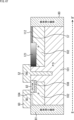
- FIG. 1 is a diagram illustrating an example of the configuration of an embodiment of an imaging device to which the present technology is applied.
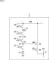
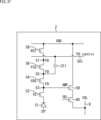
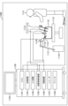
- FIG. 2 is a diagram illustrating an example of a circuit configuration of a pixel.
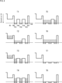
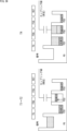
- FIG. 2 is a diagram for explaining the operation of a pixel.
- FIG. 2 is a diagram for explaining the operation of a pixel.
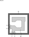
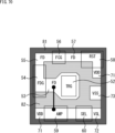
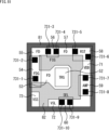
- FIG. 2 is a diagram illustrating an example of a planar configuration of a pixel according to the first embodiment.
- FIG. 2 is a diagram illustrating an example of a planar configuration of a pixel according to the first embodiment.
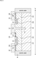
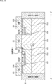
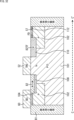
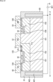
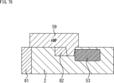
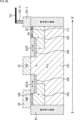
- FIG. 2 is a diagram illustrating an example of a cross-sectional configuration of a pixel according to the first embodiment.
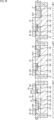
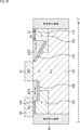
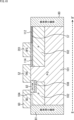
- FIG. 2 is a diagram illustrating an example of a cross-sectional configuration of a pixel according to the first embodiment.
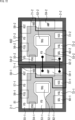
- FIG. 13 is a diagram illustrating an example of a planar configuration of a pixel according to the second embodiment.
- FIG. 13 is a diagram illustrating an example of a planar configuration of a pixel according to the third embodiment.
- FIG. 13 is a diagram illustrating an example of a cross-sectional configuration of a pixel according to a third embodiment.
- FIG. 13 is a diagram for explaining the position of a contact.
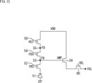
- FIG. 13 is a diagram illustrating an example of a circuit configuration of a pixel according to a fourth embodiment.
- FIG. 13 is a diagram illustrating an example of a planar configuration of a pixel according to a fourth embodiment.
- FIG. 13 is a diagram illustrating an example of a planar configuration of a pixel according to a fourth embodiment.
- FIG. 13 is a diagram illustrating an example of a circuit configuration of a pixel according to a fifth embodiment.
- FIG. 23 is a diagram illustrating an example of a planar configuration of a pixel according to the fifth embodiment.
- FIG. 23 is a diagram illustrating an example of a planar configuration of a pixel according to the fifth embodiment.
- FIG. 2 is a diagram showing an example of a planar configuration of a pixel;
- FIG. 13 is a diagram for explaining a location where a strong electric field occurs.
- FIG. 13 is a diagram for explaining a location where a strong electric field occurs.
- FIG. 13 is a diagram for explaining a location where a strong electric field occurs.
- FIG. 13 is a diagram for explaining a location where a strong electric field occurs.
- FIG. 13 is a diagram for explaining a location where a strong electric field occurs.
- FIG. 23 is a diagram for explaining a location where a strong electric field occurs.
- FIG. 23 is a diagram illustrating an example of a cross-sectional configuration of a pixel according to a sixth embodiment.
- FIG. 23 is a diagram illustrating an example of a cross-sectional configuration of a pixel according to a sixth embodiment.
- FIG. 23 is a diagram illustrating an example of a cross-sectional configuration of a pixel according to a sixth embodiment.
- 11 is a diagram for explaining the depth of an element isolation portion.
- FIG. FIG. 23 is a diagram illustrating an example of a cross-sectional configuration of a pixel according to the seventh embodiment.
- FIG. 23 is a diagram illustrating an example of a cross-sectional configuration of a pixel according to the seventh embodiment.
- FIG. 23 is a diagram illustrating an example of a cross-sectional configuration of a pixel according to the seventh embodiment.
- FIG. 23 is a diagram illustrating an example of a cross-sectional configuration of a pixel according to the eighth embodiment.
- FIG. 23 is a diagram illustrating an example of a cross-sectional configuration of a pixel according to the eighth embodiment.
- FIG. 23 is a diagram illustrating an example of a cross-sectional configuration of a pixel according to a ninth embodiment.
- FIG. 23 is a diagram illustrating an example of a cross-sectional configuration of a pixel according to a ninth embodiment.
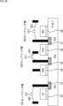
- 11 is a diagram for explaining a configuration of an element isolation unit.
- FIG. 11 is a diagram for explaining a configuration of an inter-pixel isolation section; FIG. FIG.
- FIG. 13 is a diagram for explaining the influence of dark current.
- FIG. 13 is a diagram for explaining a method for suppressing dark current.
- FIG. 23 is a diagram illustrating an example of a circuit configuration of a pixel according to a tenth embodiment.
- FIG. 2 is a diagram for explaining the operation of a pixel.
- FIG. 23 is a diagram illustrating another example of a circuit configuration of a pixel according to the tenth embodiment.
- FIG. 23 is a diagram illustrating an example of a cross-sectional configuration of a pixel according to a tenth embodiment.
- FIG. 23 is a diagram illustrating an example of a circuit configuration of a pixel according to an eleventh embodiment.
- FIG. 23 is a diagram illustrating an example of a cross-sectional configuration of a pixel according to an eleventh embodiment.
- FIG. 23 is a diagram illustrating another example of a circuit configuration of a pixel according to the eleventh embodiment.
- FIG. 23 is a diagram illustrating another example of a cross-sectional configuration of a pixel according to the eleventh embodiment.
- FIG. 23 is a diagram illustrating another example of a circuit configuration of a pixel according to the eleventh embodiment.
- FIG. 23 is a diagram illustrating another example of a cross-sectional configuration of a pixel according to the eleventh embodiment.
- FIG. 13 is a diagram for explaining locations where dark current is likely to occur.
- FIG. 13 is a diagram for explaining locations where dark current is likely to occur.
- FIG. 23 is a diagram illustrating another example of the planar configuration of a pixel in the twelfth embodiment.
- FIG. 23 is a diagram illustrating another example of a cross-sectional configuration of a pixel according to the twelfth embodiment.
- FIG. 23 is a diagram illustrating another example of the planar configuration of a pixel in the twelfth embodiment.
- FIG. 23 is a diagram illustrating another example of a cross-sectional configuration of a pixel according to the twelfth embodiment.
- FIG. 23 is a diagram showing another example of the planar configuration of a pixel in the thirteenth embodiment;
- FIG. 23 is a diagram showing another example of the planar configuration of a pixel in the fourteenth embodiment;
- FIG. 23 is a diagram showing an example of a planar configuration of a pixel when the fifth embodiment and the twelfth embodiment are combined.
- FIG. 23 is a diagram illustrating another example of a circuit configuration of a pixel according to the fifteenth embodiment.
- FIG. 23 is a diagram illustrating another example of a cross-sectional configuration of a pixel according to the sixteenth embodiment.
- FIG. 23 is a diagram illustrating another example of a cross-sectional configuration of a pixel according to the sixteenth embodiment.
- FIG. 23 is a diagram illustrating an example of a circuit configuration of a pixel according to the seventeenth embodiment.
- FIG. 23 is a diagram illustrating an example of a planar configuration of a pixel in the seventeenth embodiment.
- FIG. 23 is a diagram showing an example of a planar configuration of a pixel in the seventeenth embodiment.
- FIG. 23 is a diagram illustrating an example of a cross-sectional configuration of a pixel according to the seventeenth embodiment.
- FIG. 23 is a diagram illustrating an example of a cross-sectional configuration of a pixel according to the seventeenth embodiment.
- FIG. 23 is a diagram illustrating an example of a cross-sectional configuration of a pixel according to the seventeenth embodiment.
- FIG. 23 is a diagram illustrating an example of a cross-sectional configuration of a pixel according to the seventeenth embodiment.
- FIG. 23 is a diagram illustrating another example of a circuit configuration of a pixel according to the seventeenth embodiment.
- FIG. 23 is a diagram showing another example of the planar configuration of a pixel in the seventeenth embodiment; FIG.
- FIG. 23 is a diagram illustrating another example of a cross-sectional configuration of a pixel according to the seventeenth embodiment.
- FIG. 23 is a diagram illustrating another example of a cross-sectional configuration of a pixel according to the seventeenth embodiment.
- FIG. 23 is a diagram illustrating another example of a cross-sectional configuration of a pixel according to the seventeenth embodiment.
- FIG. 23 is a diagram illustrating another example of a cross-sectional configuration of a pixel according to the seventeenth embodiment.
- FIG. 23 is a diagram illustrating an example of a planar configuration of a pixel in the eighteenth embodiment.
- FIG. 23 is a diagram showing another example of the planar configuration of a pixel in the eighteenth embodiment; FIG.
- FIG. 23 is a diagram showing another example of the planar configuration of a pixel in the eighteenth embodiment
- FIG. 2 is a diagram showing an example of a cross-sectional configuration of a portion relating to pixel connections
- FIG. 23 is a diagram illustrating an example of a planar configuration of a pixel in the nineteenth embodiment.
- FIG. 23 is a diagram illustrating an example of a cross-sectional configuration of a pixel according to a nineteenth embodiment.
- FIG. 23 is a diagram illustrating another example of a cross-sectional configuration of a pixel according to the nineteenth embodiment.
- FIG. 23 is a diagram illustrating another example of a cross-sectional configuration of a pixel according to the nineteenth embodiment.
- FIG. 23 is a diagram illustrating another example of a cross-sectional configuration of a pixel according to the nineteenth embodiment.
- FIG. 23 is a diagram illustrating another example of a cross-sectional configuration of a pixel according to the nineteenth embodiment.
- FIG. 23 is a diagram illustrating another example of a cross-sectional configuration of a pixel according to the nineteenth embodiment.
- FIG. 23 is a diagram illustrating another example of a cross-sectional configuration of a pixel according to the nineteenth embodiment.
- FIG. 23 is a diagram illustrating an example of a planar configuration of a pixel in the twentieth embodiment.
- FIG. 23 is a diagram showing another example of the planar configuration of a pixel in the twentieth embodiment.
- FIG. 23 is a diagram showing another example of the planar configuration of a pixel in the twentieth embodiment.
- FIG. 23 is a diagram showing another example of the planar configuration of a pixel in the twentieth embodiment.
- FIG. 23 is a diagram showing another example of the planar configuration of a pixel in the twentieth embodiment.
- FIG. 23 is a diagram illustrating another example of a cross-sectional configuration of a pixel according to the twentieth embodiment.
- FIG. 23 is a diagram showing another example of the planar configuration of a pixel in the twentieth embodiment.
- FIG. 23 is a diagram illustrating another example of a cross-sectional configuration of a pixel according to the twentieth embodiment.
- FIG. 23 is a diagram showing another example of the planar configuration of a pixel in the twentieth embodiment.
- FIG. 23 is a diagram illustrating another example of a cross-sectional configuration of a pixel according to the twentieth embodiment.
- FIG. 1 is a diagram illustrating an example of the configuration of an electronic device. 1 is a diagram illustrating an example of a schematic configuration of an endoscopic surgery system.
- FIG. 1 is a block diagram showing an example of a schematic configuration of a vehicle control system
- 4 is an explanatory diagram showing an example of the installation positions of an outside-vehicle information detection unit and an imaging unit
- FIG. 1 is a block diagram showing an example of a schematic configuration of a vehicle control system
- 4 is an explanatory diagram showing an example of the installation positions of an outside-vehicle information detection unit and an imaging unit
- FIG. 1 is a block diagram showing an example of a schematic configuration of a vehicle control system
- 4 is an explanatory diagram showing an example of the installation positions of an outside-vehicle information detection unit and an imaging unit
- FIG. 1 is a block diagram showing an example of a schematic configuration of a vehicle control system
- 4 is an explanatory diagram showing an example of the installation positions of an outside-vehicle information detection unit and an imaging unit
- FIG. 1 is a block diagram showing an example of a schematic configuration of a vehicle control system
- 4 is an explanatory diagram showing an example
- FIG. 1 shows an example of the configuration of an embodiment of an imaging device to which the present technology is applied.
- the imaging device 1 in FIG. 1 is configured with a pixel array section 3 in which pixels 2 are arranged in a two-dimensional array, and a peripheral circuit section around the pixel array section.
- the peripheral circuit section includes a vertical drive circuit 4, a column signal processing circuit 5, a horizontal drive circuit 6, an output circuit 7, a control circuit 8, etc.
- the pixel 2 includes a photodiode as a photoelectric conversion element and a number of pixel transistors.
- the pixel transistors include, for example, a transfer transistor, a selection transistor, a reset transistor, an amplification transistor, and the like, and are configured as MOS transistors.
- the control circuit 8 receives an input clock and data that commands the operating mode, etc., and outputs data such as internal information of the imaging device 1. That is, the control circuit 8 generates clock signals and control signals that serve as the basis for the operation of the vertical drive circuit 4, column signal processing circuit 5, horizontal drive circuit 6, etc., based on the vertical synchronization signal, horizontal synchronization signal, and master clock. The control circuit 8 outputs the generated clock signals and control signals to the vertical drive circuit 4, column signal processing circuit 5, horizontal drive circuit 6, etc.
- the vertical drive circuit 4 is configured, for example, by a shift register, selects a specific pixel drive line 10, supplies a pulse to the selected pixel drive line 10 for driving the pixels 2, and drives the pixels 2 row by row.
- the vertical drive circuit 4 selects and scans each pixel 2 in the pixel array section 3 vertically in sequence row by row, and supplies a pixel signal based on the signal charge generated in the photoelectric conversion section of each pixel 2 according to the amount of light received to the column signal processing circuit 5 via the vertical signal line 9.
- the column signal processing circuit 5 is arranged for each column of pixels 2, and performs signal processing such as noise removal for each pixel column on the signals output from one row of pixels 2.
- the column signal processing circuit 5 performs signal processing such as CDS (Correlated Double Sampling) or DDS (double data sampling) to remove pixel-specific fixed pattern noise, and AD conversion.
- the horizontal drive circuit 6 is, for example, configured with a shift register, and by sequentially outputting horizontal scanning pulses, selects each of the column signal processing circuits 5 in turn, and causes each of the column signal processing circuits 5 to output a pixel signal to the horizontal signal line 11.
- the output circuit 7 processes and outputs the signals sequentially supplied from each of the column signal processing circuits 5 through the horizontal signal line 11.
- the output circuit 7 may perform only buffering, or may perform black level adjustment, column variation correction, various digital signal processing, etc.
- the input/output terminal 13 exchanges signals with the outside.
- the imaging device 1 configured as described above is a CMOS image sensor with a so-called column AD system in which a column signal processing circuit 5 that performs CDS processing or DDS processing and AD conversion processing is arranged for each pixel column.
- ⁇ Pixel circuit configuration example> We will now explain the configuration of a unit pixel provided in the pixel array section 3.
- the unit pixel provided in the pixel array section 3 is configured, for example, as shown in Fig. 2.
- Fig. 2 the same reference numerals are used to designate parts corresponding to those in Fig. 1, and their description will be omitted as appropriate.
- Pixel 2 which is a unit pixel, has a photoelectric conversion section 51, a first transfer transistor 52, a first FD (Floating Diffusion) section 53, a second transfer transistor 54, a second FD section 55, a third transfer transistor 56, a third FD section 57, a reset transistor 58, an amplification transistor 59, and a selection transistor 60.
- a photoelectric conversion section 51 a first transfer transistor 52, a first FD (Floating Diffusion) section 53, a second transfer transistor 54, a second FD section 55, a third transfer transistor 56, a third FD section 57, a reset transistor 58, an amplification transistor 59, and a selection transistor 60.
- drive lines are wired for each pixel row as pixel drive lines 10 for the pixels 2.
- Drive signals TRG, FDG, FCG, RST, and SEL are supplied from the vertical drive circuit 4 to the first transfer transistor 52, the second transfer transistor 54, the third transfer transistor 56, the reset transistor 58, and the selection transistor, respectively, via the multiple drive lines.
- These drive signals are pulse signals that are active when they are at a high level (e.g., power supply voltage VDD) and inactive when they are at a low level (e.g., negative potential). That is, when each of the drive signals TRG through SEL is at a high level, the transistor to which it is supplied is conductive, i.e., on, and when each drive signal is at a low level, the transistor to which it is supplied is non-conductive, i.e., off.
- VDD power supply voltage
- the photoelectric conversion unit 51 is composed of, for example, a PN junction photodiode.
- the photoelectric conversion unit 51 receives incident light, performs photoelectric conversion, and accumulates the resulting electric charge.
- the first transfer transistor 52 is provided between the photoelectric conversion section 51 and the first FD section 53, and a drive signal TRG is supplied to the gate electrode of the first transfer transistor 52.
- this drive signal TRG becomes high level, the first transfer transistor 52 is turned on, and the charge stored in the photoelectric conversion section 51 is transferred to the first FD section 53 via the first transfer transistor 52.
- the first FD section 53, the second FD section 55, and the third FD section 57 are each floating diffusion regions called floating diffusions, and function as storage sections that temporarily store transferred charges and charges that overflow from the photoelectric conversion section 51.
- the second transfer transistor 54 is provided between the first FD section 53 and the second FD section 55, and a drive signal FDG is supplied to the gate electrode of the second transfer transistor 54.
- a drive signal FDG becomes high level, the second transfer transistor 54 is turned on, and the charge from the first FD section 53 is transferred to the second FD section 55 via the second transfer transistor 54.
- the second transfer transistor 54 When the second transfer transistor 54 is turned on, the area in which the electric charges are accumulated becomes the combined area of the first FD section 53 and the second FD section 55, and the conversion efficiency when converting the electric charges generated in the photoelectric conversion section into a voltage can be switched.
- the second transfer transistor 54 functions as a conversion efficiency switching transistor that switches the conversion efficiency.
- the third transfer transistor 56 is provided between the second FD section 55 and the third FD section 57, and a drive signal FCG is supplied to the gate electrode of the third transfer transistor 56.
- a drive signal FCG becomes high level, the third transfer transistor 56 is turned on, and the charge from the second FD section 55 is transferred to the third FD section 57 via the third transfer transistor 56.
- the third transfer transistor 56 When the third transfer transistor 56 is turned on, the area in which the electric charges are accumulated becomes the combined area of the first FD section 53, the second FD section 55, and the third FD section 57, and the conversion efficiency when converting the electric charges generated in the photoelectric conversion section into a voltage can be switched.
- the third transfer transistor 56 functions as a conversion efficiency switching transistor that switches the conversion efficiency.
- the MIM capacitance element is a trench-type capacitor, and has, for example, a U-shaped three-dimensional structure, which allows a relatively large capacitance to be obtained in a small mounting area. It is also possible to use capacitance elements other than the MIM capacitance element, such as a MOM (Metal Oxide Metal) capacitance element, a poly-poly capacitance element (a capacitance element in which both opposing electrodes are made of polysilicon), or an additional capacitance including a parasitic capacitance formed by wiring.
- MOM Metal Oxide Metal
- the reset transistor 58 is connected between the power supply VDD and the third FD section 57, and a drive signal RST is supplied to the gate electrode of the reset transistor 58.
- the drive signal RST is set to a high level, the reset transistor 58 is turned on and the potential of the third FD section 57 is reset to the level of the power supply voltage VDD.
- the amplifying transistor 59 has a gate electrode connected to the first FD section 53 and a drain connected to a power supply VDD, and serves as the input section of a read circuit that reads out a signal corresponding to the charge held in the first FD section 53, a so-called source follower circuit.
- the amplifying transistor 59 has a source connected to the vertical signal line 9 via the selection transistor 60, and thus constitutes a source follower circuit together with a constant current source (not shown) connected to one end of the vertical signal line 9.
- the selection transistor 60 is connected between the source of the amplification transistor 59 and the vertical signal line 9, and a drive signal SEL is supplied to the gate electrode of the selection transistor 60.
- the drive signal SEL is set to a high level, the selection transistor 60 is turned on and the pixel 2 is placed in a selected state.
- the pixel signal output from the amplification transistor 59 is output to the vertical signal line 9 via the selection transistor 31.
- each drive signal when each drive signal is in an active state, i.e. at a high level, it is also referred to as the drive signal being on, and when each drive signal is in an inactive state, i.e. at a low level, it is also referred to as the drive signal being off.
- the pixel 2 shown in FIG. 2 has a first FD section 53, a second FD section 55, and a third FD section 57. These FD sections are connected in series, and the conversion efficiency when converting the charge generated in the photoelectric conversion section into a voltage can be switched between three levels.
- High conversion efficiency is composed of the first FD section 53.
- Medium conversion efficiency is composed of (first FD section 53 + second FD section 55).
- Low conversion efficiency is composed of (first FD section 53 + second FD section 55 + third FD section 57).
- the charge stored in the photoelectric conversion section 51 is received by the first FD section 53 (high conversion efficiency) or (first FD section 53 + second FD section 55) (medium conversion efficiency) and output.
- the charge stored in the photoelectric conversion section 51 overflows beyond the first transfer transistor 52 and into the first FD section 53, and is stored in the first FD section 53, the second FD section 55, and the third FD section 57.
- the conversion efficiency is high and charge is accumulated in the first FD section 53, and when the received light amount is large and the signal is large, the conversion efficiency is low and charge is accumulated in (first FD section 53 + second FD section 55 + third FD section 57).
- a medium conversion efficiency is further provided between the high conversion efficiency and the low conversion efficiency, and a conversion efficiency is provided in which charge is accumulated in (first FD section 53 + second FD section 55).
- the charge that has overflowed the photoelectric conversion unit 51 and accumulated in the first FD unit 53, the second FD unit 55, and the third FD unit 57 is received and output by (the first FD unit 53 + the second FD unit 55 + the third FD unit 57) together with the charge accumulated in the photoelectric conversion unit 51.
- the high, medium, and low conversion efficiency readouts are AD converted separately, and which readout signal is used is determined from the amount of each readout signal.
- the two readout signals may be blended and used. Using a blended signal suppresses image quality degradation at the junction.
- Fig. 3 is a timing chart for explaining the operation of the pixel 2
- Fig. 4 is a potential diagram for explaining the operation of the pixel 2.
- HGC high conversion efficiency
- MCG medium conversion efficiency
- LCG bottom-to-bottom efficiency
- PD PD 51
- TRG stands for the first transfer transistor 52
- FD1 stands for the first FD section 53
- FDG stands for the second transfer transistor 54
- FD2 stands for the second FD section 55
- FCG stands for the third transfer transistor 56
- FD3 stands for the third FD section 57
- RST stands for the reset transistor 58.
- Time T1 is the time immediately after the shutter operation is performed. Referring to FIG. 3, immediately after the shutter operation is performed, the drive signal SEL supplied to the selection transistor 60, the drive signal RST supplied to the reset transistor 58, the drive signal FCG supplied to the third transfer transistor 56, the drive signal FDG supplied to the second transfer transistor 54, and the drive signal TRG supplied to the first transfer transistor 52 are all in the off state.
- the PD 51, the first FD section 53, the second FD section 55, and the third FD section 57 are in an off state, and no signal is stored.
- the exposure period begins at time T1, photoelectric conversion is performed in PD 51, and a signal is accumulated in PD 51. If the signal exceeds the number of saturation electrons, it overflows below the first transfer transistor 52, and the signal is accumulated in the first FD section 53, the second FD section 55, and the third FD section 57 according to the amount of the overflowed signal.
- Time T2 is the reset period of the MCG (medium conversion efficiency) mode.
- the drive signal SEL supplied to the selection transistor 60 and the drive signal FDG supplied to the second transfer transistor 54 are turned on.
- FIG. 4 shows a state in which a signal that has overflowed from PD 51 is stored in the first FD section 53 and the second FD section 55.
- the reset period of the HCG (high conversion efficiency) mode starts at time T3.
- the drive signal SEL supplied to the selection transistor 60 is maintained in the on state, and the drive signal FDG supplied to the second transfer transistor 54 is switched from on to off.
- the system transitions to the readout period of the HCG mode at time T4.
- the drive signal TRG supplied to the first transfer transistor 52 is turned on for a predetermined period of time.
- the signal stored in the PD 51 is read out by the first transfer transistor 52.
- the readout from the PD 51 is performed by CDS (correlated double sampling) drive.
- Image data in HCG mode is generated and output by CDS drive using the reset signal obtained during the reset period of HCG mode at time T3 and the signal read out during the readout period of HCG mode at time T4.
- a readout is performed in HDG mode, so that the signal stored in PD 51 is read out and the PD 51 is emptied, and signals corresponding to the signal stored in PD 51 are stored in the first FD section 53, the second FD section 55, and the third FD section 57.
- the MCG mode readout period begins at time T5.
- the drive signal FDG supplied to the second transfer transistor 54 is turned on.
- the drive signal FDG By turning on the drive signal FDG, the charges stored in the first FD section 53 and the second FD section 55 are read out.
- image data for MCG mode is generated and output by CDS drive using the reset signal obtained during the reset period of MCG mode at time T2 and the signal read out during the readout period of MCG mode at time T5.
- the system transitions to the LCG mode readout period at time T6.
- the drive signal FCG supplied to the third transfer transistor 56 is turned on.
- the second transfer transistor 54 and the third transfer transistor 56 are in the on state.
- the process moves to the reset period at time T7.
- a reset operation is performed in the same state as when the shutter was pressed, so that the black level signal during the reset period in LCG mode at time T8 is made the same as the black level signal when the shutter was pressed.
- the drive signal SEL supplied to the selection transistor 60 is kept in the off state from time T6 to time T8.
- the drive signal RST supplied to the reset transistor 58 is kept in the on state for a predetermined time from time T6 to time T8.
- the drive signal FCG supplied to the third transfer transistor 56 is kept in the on state for a predetermined time from time T6 to time T8.
- the drive signal FDG supplied to the second transfer transistor 54 is kept in the on state for a predetermined time from time T6 to time T8.
- the signals stored in the first FD section 53, the second FD section 55, and the third FD section 57 are reset, as shown in FIG. 4.
- DDS double data sampling
- the signal read out during the readout period in LCG mode at time T6 and the reset signal read out during the reset period in LCG mode at time T8 are used to generate and output image data in LCG mode.
- the drive signals SEL, FCG, and FDG are turned off.
- the signal at HCG high conversion efficiency
- the signal at MCG medium conversion efficiency
- the signal at LCG low conversion efficiency
- FIG. 5 is a diagram showing an example of a planar configuration of the surface of a silicon substrate on which the transistors of the pixel 2 are arranged.
- a gate electrode TRG of the first transfer transistor 52 is formed near the center of the pixel 2.
- the gates of the transistors included in the pixel 2 other than the first transfer transistor 52 are arranged around the gate electrode TRG of the first transfer transistor 52.
- a gate electrode FDG of the second transfer transistor 54 is formed to the left of the gate electrode TRG of the first transfer transistor 52.
- a first FD portion 53 formed of an N+ diffusion layer is provided in the silicon substrate.
- a gate electrode FCG of a third transfer transistor 56 is formed above the gate electrode TRG of the first transfer transistor 52 in the figure.
- a second FD section 55 is provided between the second transfer transistor 54 and the third transfer transistor 56.
- the gate electrode RST of the reset transistor 58 is formed on the upper right side of the gate electrode TRG of the first transfer transistor 52.
- a third FD section 57 is formed between the third transfer transistor 56 and the reset transistor 58.
- the gate electrode AMP of the amplifier transistor 59 is formed on the right side of the gate electrode TRG of the first transfer transistor 52 in the figure. Between the reset transistor 58 and the amplifier transistor 59, a VDD region 71 is formed of a P+ diffusion layer and is connected to the power supply voltage VDD.
- the gate electrode SEL of the selection transistor 60 is formed below the gate electrode TRG of the first transfer transistor 52 in the figure.
- a VSL region connected to the vertical signal line 9 is formed on the left side of the selection transistor 60 in the figure.
- a VSS region 73 made of a P+ diffusion layer is formed on the lower left side of the first transfer transistor 52 in the figure.
- the inter-pixel isolation section 81 is formed to surround the pixel 2. For example, it is formed by FFTI (Front Full Trench Isolation).
- the inter-pixel isolation section 81 can be formed by a trench that penetrates or does not penetrate the semiconductor substrate.
- the inter-pixel isolation section 81 isolates the pixels 2 with an insulator, and each pixel 2 is electrically isolated.
- a device isolation section 82 is formed between the transistors that make up pixel 2.
- the device isolation section 82 is, for example, a structure in which a trench of a predetermined depth is formed in the device isolation region and an insulating film is embedded therein, or a region formed by ion implantation.
- Pixel 2 has an inter-pixel isolation section 81 in the pixel boundary region, and is isolated by an element isolation section 82 in the active region.
- the active region is the region shown in white in the figure, and is configured in a shape that connects from under the gate electrode TRG of the first transfer transistor 52 to the VSL region 72.
- a part of the element isolation portion 82 is configured to be in contact with the inter-pixel isolation portion 81.
- the element isolation portion 82 between the second transfer transistor 54 and the VSS region 73, and the element isolation portion 82 between the VSS region 73 and the VSL region 72 are configured to be in contact with the inter-pixel isolation portion 81.
- the pixel transistors other than the first transfer transistor 52 are provided not only on the element isolation section 82 as element isolation, but also on the inter-pixel isolation section 81.
- the gate electrodes of the pixel transistors other than the first transfer transistor 52 are configured to overlap the inter-pixel isolation portion 81, as shown in FIG. 5.
- a partial area of the gate electrode of the pixel transistor is configured to have an area that overlaps the inter-pixel isolation portion 81 in a planar view. By configuring it to overlap the inter-pixel isolation portion 81, it is possible to secure an area for the electrode gate.
- the gate electrodes of the pixel transistors other than the first transfer transistor 52 are configured to overlap the element isolation section 82 as well, as shown in FIG. 5. In other words, a portion of the gate electrodes of the pixel transistors is configured to have an area that overlaps with the element isolation section 82 in a plan view.
- the left side of the gate electrode FDG of the second transfer transistor 54 in the figure overlaps with the inter-pixel isolation section 81 in a planar view, and a part of the right-left side and the lower side of the figure overlap with the element isolation section 82 in a planar view.
- the upper side of the gate electrode FCG of the third transfer transistor 56 in the figure overlaps with the inter-pixel isolation section 81 in a planar view, and the lower side of the figure overlaps with the element isolation section 82 in a planar view.
- the upper and right sides of the gate electrode RST of the reset transistor 58 overlap the inter-pixel isolation portion 81 in a planar view, and a part of the left side and a part of the lower side (bottom left) of the gate electrode RST of the reset transistor 58 overlap the element isolation portion 82 in a planar view.
- the right side of the gate electrode AMP of the amplifier transistor 59 overlaps the inter-pixel isolation portion 81 in a planar view, and the left side of the gate electrode AMP of the amplifier transistor 59 overlaps the element isolation portion 82 in a planar view.
- the lower side of the gate electrode SEL of the selection transistor 60 overlaps with the inter-pixel isolation portion 81 in a planar view, and the upper side of the gate electrode SEL overlaps with the element isolation portion 82 in a planar view.
- each transistor included in pixel 2 other than first transfer transistor 52 is arranged to surround the first transfer transistor. Furthermore, each transistor included in pixel 2 other than first transfer transistor 52 is configured so that at least one side overlaps with inter-pixel isolation section 81 in a plan view, and the side opposite to the side overlapping with inter-pixel isolation section 81 overlaps with element isolation section 82.
- the WL dimension of the pixel transistor that can be arranged per pixel can be expanded, making it possible to design the pixel transistor to have small cutoff variations and amplification noise.
- the first transfer transistor 52 which transfers the charge converted by the photoelectric conversion unit 51 to the FD unit, is arranged in the center of the pixel 2, i.e., in the center of the photoelectric conversion unit 51, making it possible to easily transfer the signal from the photoelectric conversion unit 51 to the first FD unit 53.
- Fig. 6 shows a diagram in which a line segment AA' is added to the pixel 2 shown in Fig. 5.
- Fig. 7 shows an example of a cross-sectional configuration of the pixel 2 shown in Fig. 6 along the line segment AA'.
- pixel 2 comprises a semiconductor substrate 80 and a multilayer wiring layer (not shown) formed on its front surface side (upper side in the figure).
- the lower side is the light incident surface side, on which an on-chip lens, color filter, etc. (not shown) are provided.
- the upper side is the wiring layer side, on which multiple transistors are formed.
- the semiconductor substrate 80 is made of, for example, silicon (hereinafter referred to as Si) and is formed to have a thickness of, for example, 1 to 10 ⁇ m.
- Si silicon
- an N-type (second conductivity type) semiconductor region 101 is formed in a pixel unit in a P-type (first conductivity type) semiconductor region 102, thereby forming a photodiode PD in a pixel unit.
- inter-pixel separation sections 81 are formed from the back side (light incident surface side) of the semiconductor substrate 80 to a predetermined depth in the substrate depth direction, separating adjacent pixels in the depth direction of the semiconductor substrate 80.
- the depth in the substrate thickness direction at which the inter-pixel separation sections 81 are formed can be any depth, and the example shown in FIG. 7 shows a case in which the inter-pixel separation sections 81 penetrate the semiconductor substrate 80 from the back side to the front side, completely separating pixels.
- the outer periphery including the side walls of the inter-pixel separation sections 81 can also be configured to be covered with an anti-reflection film formed of a layer including a hafnium oxide film.
- the inter-pixel separation sections 81 can also be configured to have the function of preventing incident light from penetrating into the adjacent pixel 2, confining it within the own pixel, and preventing incident light from leaking in from the adjacent pixel 2.
- one first transfer transistor 52 is formed for one photodiode PD formed in each pixel 2.
- the gate electrode TRG of the first transfer transistor 52 is connected to the N-type region of the photodiode PD.
- an N+ region 105 that is the first FD section 53 is formed on the left side of the first transfer transistor 52 in the figure.
- a device isolation section 82 is formed on the left side of the first FD section 53 in the figure.
- This device isolation section 82 is formed of, for example, an oxide film, and is provided to isolate the transistors of the pixel 2.
- a pinning film 107 is formed below the device isolation section 82.
- the pinning film 107 is formed at the boundary between the device isolation section 82 and the P-type semiconductor region 102, and is, for example, a fixed charge film having a negative fixed charge.
- the pinning film 107 is formed using, for example, hafnium oxide (HfO2), zirconium dioxide (ZrO2), tantalum oxide (Ta2O5), etc.
- a positive charge (hole) accumulation region is formed at the boundary of the silicon semiconductor substrate 80, which makes it possible to suppress the generation of dark current.
- a selection transistor 60 is formed on the left side of the element isolation section 82 in the figure, and a channel 104 is formed in an N-type region below the gate electrode SEL of the selection transistor 60.
- the gate electrode SEL of the selection transistor 60 is positioned and sized so that one side has an area that overlaps with the element isolation portion 82 and the other side has an area that overlaps with the pixel isolation portion 81.
- the gate electrode SEL is shown in FIG. 7 as a rectangle, this rectangle may or may not include sidewalls.
- the gate electrode SEL may be configured so that a portion of it, including the sidewalls, overlaps with the element isolation portion 82 and also overlaps with the pixel isolation portion 81. The same applies to the other transistors.
- An element isolation section 82 is formed on the right side of the first transfer transistor 52 in the figure, and a pinning film 108 is formed below the element isolation section 82.
- An amplifier transistor 59 is formed on the right side of this element isolation section 82 in the figure.
- a channel 106 is formed in an N-type region below the gate electrode AMP of the amplifier transistor 59.
- the gate electrode AMP of the amplifying transistor 59 is formed at a position and size such that one side has an area that overlaps with the element isolation section 82, and the other side has an area that overlaps with the pixel isolation section 81.
- the transistors arranged around the first transfer transistor 52 for example, the selection transistor 60 and the amplification transistor 59 in FIG. 7, are configured so that one side is on the inter-pixel isolation section 132 and the other side is on the element isolation section 82.
- the gate electrode TRG of the first transfer transistor 52 may also be configured so that the gate is provided in the vertical direction as shown in FIG. 8.
- the photodiode PD is configured as a buried type photodiode PD, and a part of the gate electrode TRG of the first transfer transistor 52 is provided up to a part of the photodiode PD.
- the gate electrode TRG of the first transfer transistor 52 has a gate (a gate arranged in the horizontal direction) provided on the surface of the semiconductor substrate 80, and a gate (a gate arranged in the vertical direction) provided within the N-type semiconductor region 101 of the photodiode PD in the semiconductor substrate 80.
- first transfer transistor 52 is a vertical transistor, but this technology can also be applied when transistors other than the first transfer transistor 52 are vertical transistors.
- Second Embodiment Fig. 9 is a diagram showing an example of the planar configuration of the pixel 2 according to the second embodiment.
- parts similar to those of the pixel 2 according to the first embodiment shown in Fig. 5 are denoted by the same reference numerals, and descriptions thereof will be omitted as appropriate.
- the pixel 2 shown in FIG. 9 is different from the pixel 2 shown in FIG. 5 in that a part of the element isolation portion 82 is formed by ion implantation, but is otherwise similar.
- the element isolation section 82 provided between the VSL region 72 and the VSS region 73 is the element isolation section 131-1 formed by ion implantation. Also, in the pixel 2 shown in FIG. 9, the element isolation section 82 provided between the VSS region 73 and the second transfer transistor 54 is the element isolation section 131-2 formed by ion implantation.
- the element isolation portion 131 is, for example, an element isolation portion formed by doping a P-type impurity into the semiconductor substrate 80.
- the element isolation portion 82 in the region that contacts the inter-pixel isolation portion 81 is the element isolation portion 131 formed by ion implantation. In this way, by forming the element isolation portion 82 in the region that contacts the inter-pixel isolation portion 81 by ion implantation, manufacturing is made easier.
- Third Embodiment Fig. 10 is a diagram showing an example of the planar configuration of the pixel 2 according to the third embodiment.
- parts similar to those of the pixel 2 according to the first embodiment shown in Fig. 5 are denoted by the same reference numerals, and descriptions thereof will be omitted as appropriate.
- the pixel 2 shown in FIG. 10 is different from the pixel 2 shown in FIG. 5 in that the entire element isolation portion 82 is an area formed by ion implantation, but is otherwise similar.
- the element isolation portion 82 is an element isolation portion 131 formed by ion implantation.
- the element isolation portion 131 is an element isolation portion formed by doping, for example, a P-type impurity into the semiconductor substrate 80.
- the element isolation section can be configured as element isolation section 131 formed by ion implantation.
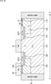
- FIG. 11 is a diagram showing an example of the cross-sectional configuration of pixel 2 taken along line segment A-A' shown in FIG. 10.
- the example of the cross-sectional configuration of pixel 2 shown in FIG. 11 is similar to the example of the cross-sectional configuration of pixel 2 shown in FIG. 7, except that element isolation portion 82 is replaced by element isolation portion 131.
- the element isolation section 131 provided between the first FD section 53 and the selection transistor 60 is an element isolation section formed by ion implantation.
- the element isolation section 131 provided between the first transfer transistor 52 and the amplification transistor 59 is an element isolation section formed by ion implantation.
- the element isolation portion can be configured as a region doped with, for example, P-type impurities, formed by ion implantation.
- Fig. 12 is a diagram for explaining the position of a contact for fixing the substrate potential for each pixel.
- Fig. 12 shows an example of a cross-sectional configuration of a pixel 2, which basically has the same configuration as the example of the cross-sectional configuration of the pixel 2 shown in Fig. 7.
- the contact for supplying the substrate potential can be configured to be shared from the back surface side.
- contacts 151 are provided on the lower side (back surface side) of the left and right sides of the figure. These contacts 151 are connected to a P+ layer with a high concentration of P-type impurities formed on the side of the inter-pixel isolation section 81. These contacts 151 are connected, for example, to the power supply voltage VSS, and are connected to a point in pixel 2 that supplies the voltage VSS.
- Fig. 13 is a diagram showing a circuit configuration example of the pixel 2 in the fourth embodiment.
- the pixel 2 in the first to third embodiments described above has been described using a configuration example having three FD sections, but the present technology can also be applied to a configuration having two FD sections as shown in Fig. 13.
- parts similar to those in the circuit diagram of the pixel 2 shown in Fig. 2 are denoted by the same reference numerals, and descriptions thereof will be omitted as appropriate.
- the pixel 2 shown in FIG. 13 has a configuration in which the third transfer transistor 56 and the third FD section 57 are deleted from the pixel 2 shown in FIG. 2. That is, the pixel 2 shown in FIG. 13 has a photoelectric conversion section 51, a first transfer transistor 52, a first FD section 53, a second transfer transistor 54, a second FD section 55, a reset transistor 58, an amplification transistor 59, and a selection transistor 60.
- the photoelectric conversion unit 51 is composed of, for example, a PN junction photodiode, receives incident light, performs photoelectric conversion, and accumulates the resulting electric charge.
- the first transfer transistor 52 is provided between the photoelectric conversion unit 51 and the first FD unit 53, and a drive signal TRG is supplied to the gate electrode of the first transfer transistor 52. When this drive signal TRG becomes high level, the first transfer transistor 52 is turned on, and the electric charge accumulated in the photoelectric conversion unit 51 is transferred to the first FD unit 53 via the first transfer transistor 52.
- the second transfer transistor 54 is provided between the first FD section 53 and the second FD section 55, and a drive signal FDG is supplied to the gate electrode of the second transfer transistor 54.
- a drive signal FDG becomes high level, the second transfer transistor 54 is turned on, and the charge from the first FD section 53 is transferred to the second FD section 55 via the second transfer transistor 54.
- the second transfer transistor 54 When the second transfer transistor 54 is turned on, the area in which the electric charges are accumulated becomes the combined area of the first FD section 53 and the second FD section 55, and the conversion efficiency when converting the electric charges generated in the photoelectric conversion section into a voltage can be switched.
- the second transfer transistor 54 functions as a conversion efficiency switching transistor that switches the conversion efficiency, and functions as a switch that turns the conversion efficiency on and off.
- the reset transistor 58 is connected between the power supply VDD and the second FD section 55, and a drive signal RST is supplied to the gate electrode of the reset transistor 58.
- the drive signal RST is set to a high level, the reset transistor 58 is turned on and the potential of the second FD section 55 is reset to the level of the power supply voltage VDD.
- the amplifying transistor 59 has a gate electrode connected to the first FD section 53 and a drain connected to a power supply VDD, and serves as the input section of a read circuit that reads out a signal corresponding to the charge held in the first FD section 53, a so-called source follower circuit.
- the amplifying transistor 59 has a source connected to the vertical signal line 9 via the selection transistor 60, and thus constitutes a source follower circuit together with a constant current source (not shown) connected to one end of the vertical signal line 9.
- the selection transistor 60 is connected between the source of the amplification transistor 59 and the vertical signal line 9, and a drive signal SEL is supplied to the gate electrode of the selection transistor 60.
- the drive signal SEL is set to a high level, the selection transistor 60 is turned on and the pixel 2 is placed in a selected state. As a result, the pixel signal output from the amplification transistor 59 is output to the vertical signal line 9 via the selection transistor 60.
- FIG. 14 is a diagram showing an example of a planar configuration of the surface of a silicon substrate on which transistors of the pixel 2 having the circuit configuration shown in FIG. 13 are arranged.
- the gate electrode TRG of the first transfer transistor 52 is formed near the center of the pixel 2.
- the gate electrodes TRG of the first transfer transistor 52 are centered around the gate electrode TRG of the first transfer transistor 52, and the gates of the transistors other than the first transfer transistor 52 included in the pixel 2 are arranged. In other words, the first transfer transistor 52 is centered, and the transistors constituting the pixel 2 other than the first transfer transistor 52 are arranged around the first transfer transistor 52.
- the gate electrode FDG of the second transfer transistor 54 is formed to the left of the gate electrode TRG of the first transfer transistor 52. Between the gate electrodes TRG and FDG, a first FD section 53 formed of an N+ diffusion layer is provided in the silicon substrate.
- a gate electrode RST of the reset transistor 58 is formed above the gate electrode TRG of the first transfer transistor 52 in the figure.
- a second FD section 55 is formed between the second transfer transistor 54 and the reset transistor 58.
- the gate electrode AMP of the amplifier transistor 59 is formed on the right side of the gate electrode TRG of the first transfer transistor 52 in the figure.
- a VDD region 71 that is connected to the power supply voltage VDD is formed between the reset transistor 58 and the amplifier transistor 59.
- the gate electrode SEL of the selection transistor 60 is formed below the gate electrode TRG of the first transfer transistor 52 in the figure.
- a VSL region connected to the vertical signal line 9 is formed on the left side of the selection transistor 60 in the figure.
- a VSS region 73 made of a P+ diffusion layer is formed on the lower left side of the first transfer transistor 52 in the figure.
- inter-pixel isolation sections 81 are formed between the pixels 2, inter-pixel isolation sections 81 are formed. Between each transistor, an element isolation section 82 is formed.
- the element isolation section 82 has a structure in which, for example, a trench of a predetermined depth is formed in the element isolation region and an insulating film is embedded therein. As described with reference to FIG. 10, it may also be an element isolation section 131 formed by ion implantation.
- An inter-pixel isolation section 81 is provided in the pixel boundary region of pixel 2, and the active region is isolated by an element isolation section 82.
- the active region is formed as a continuous region (connected region). In the example shown in FIG. 14, the active region is formed as a continuous region from under the gate electrode TRG of the first transfer transistor 52 to the VSL region 72.
- the element isolation section 82 is structured so that a portion of it contacts the inter-pixel isolation section 81.
- the gate electrodes of the pixel transistors other than the first transfer transistor 52 are configured to overlap the inter-pixel isolation portion 81, as shown in FIG. 14.
- a partial area of the gate electrode of the pixel transistor is configured to have an area that overlaps the inter-pixel isolation portion 81 in a planar view. By configuring it to overlap the inter-pixel isolation portion 81, it is possible to secure an area for the electrode gate.
- the gate electrodes of the pixel transistors other than the first transfer transistor 52 are configured to overlap the element isolation section 82 as well, as shown in FIG. 14. In other words, a portion of the gate electrode of the pixel transistor is configured to have an area that overlaps with the element isolation section 82 in a plan view.
- the left side of the gate electrode FDG of the second transfer transistor 54 in the figure overlaps with the inter-pixel isolation portion 81 in a planar view, and the right side of the figure overlaps with the element isolation portion 82 in a planar view.
- the upper side of the gate electrode RST of the reset transistor 58 in the figure overlaps with the inter-pixel isolation portion 81 in a planar view, and the lower side of the figure overlaps with the element isolation portion 82 in a planar view.
- the right side of the gate electrode AMP of the amplifying transistor 59 overlaps with the inter-pixel isolation portion 81 in a planar view, and the left side of the gate electrode AMP overlaps with the element isolation portion 82 in a planar view.
- the lower side of the gate electrode SEL of the selection transistor 60 overlaps with the inter-pixel isolation portion 81 in a planar view, and the upper side of the gate electrode SEL overlaps with the element isolation portion 82 in a planar view.
- each transistor included in pixel 2 other than first transfer transistor 52 is arranged to surround first transfer transistor 52. Furthermore, each transistor included in pixel 2 other than first transfer transistor 52 is configured so that at least one side overlaps inter-pixel isolation portion 81 in a plan view, and the side opposite to the side overlapping inter-pixel isolation portion 81 overlaps element isolation portion 82.
- the WL dimension of the pixel transistor that can be arranged per pixel can be expanded, making it possible to design the pixel transistor to have small cutoff variations and amplification noise.
- the first transfer transistor 52 which transfers the charge converted by the photoelectric conversion unit 51 to the FD unit, is arranged in the center of the pixel 2, i.e., in the center of the photoelectric conversion unit 51, making it possible to easily transfer the signal from the photoelectric conversion unit 51 to the first FD unit 53.
- the number of transistors arranged is smaller than in the pixel 2 shown in FIG. 5, so each transistor can be made larger.
- the amplification transistor 59 can be made larger, making it possible to reduce noise.
- Fifth embodiment 15 is a diagram showing an example of a circuit configuration of a pixel 2 according to the fifth embodiment.
- the pixel 2 according to the fifth embodiment has three FD sections, similar to the pixel 2 according to the first to third embodiments, and further includes an overflow transistor 201.
- the pixel 2 has a photoelectric conversion section 51, a first transfer transistor 52, a first FD section 53, a second transfer transistor 54, a second FD section 55, a third transfer transistor 56, a third FD section 57, a reset transistor 58, an amplification transistor 59, a selection transistor 60, and an overflow transistor 201.
- the overflow transistor 201 is provided between the photoelectric conversion section 51 and the third FD section 57, and is configured so that the charge that overflows from the photoelectric conversion section 51 is accumulated in the third FD section 57.
- the first transfer transistor 52 is provided between the photoelectric conversion section 51 and the first FD section 53, and a drive signal TRG is supplied to the gate electrode of the first transfer transistor 52.
- this drive signal TRG becomes high level, the first transfer transistor 52 is turned on, and the charge stored in the photoelectric conversion section 51 is transferred to the first FD section 53 via the first transfer transistor 52.
- the second transfer transistor 54 is provided between the first FD section 53 and the second FD section 55, and a drive signal FDG is supplied to the gate electrode of the second transfer transistor 54.
- a drive signal FDG becomes high level, the second transfer transistor 54 is turned on, and the charge from the first FD section 53 is transferred to the second FD section 55 via the second transfer transistor 54.
- the second transfer transistor 54 When the second transfer transistor 54 is turned on, the area in which the electric charges are accumulated becomes the combined area of the first FD section 53 and the second FD section 55, and the conversion efficiency when converting the electric charges generated in the photoelectric conversion section into a voltage can be switched.
- the third transfer transistor 56 is provided between the second FD section 55 and the third FD section 57, and a drive signal FCG is supplied to the gate electrode of the third transfer transistor 56.
- a drive signal FCG becomes high level, the third transfer transistor 56 is turned on, and the charge from the second FD section 55 is transferred to the third FD section 57 via the third transfer transistor 56.
- the third transfer transistor 56 When the third transfer transistor 56 is turned on, the area in which the electric charges are accumulated becomes the combined area of the first FD section 53, the second FD section 55, and the third FD section 57, and the conversion efficiency when converting the electric charges generated in the photoelectric conversion section into a voltage can be switched. As described above, the third FD section 57 also accumulates electric charges that have overflowed from the photoelectric conversion section 51 and been transferred via the overflow transistor 201.
- the reset transistor 58 is connected between the power supply VDD and the intersection of the second FD section 55 and the third FD section 57, and a drive signal RST is supplied to the gate electrode of the reset transistor 58.
- the drive signal RST is set to a high level, the reset transistor 58 is turned on and the potentials of the second FD section 55 and the third FD section 57 are reset to the level of the power supply voltage VDD.
- the amplifying transistor 59 has a gate electrode connected to the first FD section 53 and a drain connected to a power supply VDD, and serves as the input section of a read circuit that reads out a signal corresponding to the charge held in the first FD section 53, a so-called source follower circuit.
- the amplifying transistor 59 has a source connected to the vertical signal line 9 via the selection transistor 60, and thus constitutes a source follower circuit together with a constant current source (not shown) connected to one end of the vertical signal line 9.
- the selection transistor 60 is connected between the source of the amplification transistor 59 and the vertical signal line 9, and a drive signal SEL is supplied to the gate electrode of the selection transistor 60.
- the drive signal SEL is set to a high level, the selection transistor 60 is turned on and the pixel 2 is placed in a selected state.
- the pixel signal output from the amplification transistor 59 is output to the vertical signal line 9 via the selection transistor 31.
- FIG. 16 is a diagram showing an example of a planar configuration of a silicon substrate surface on which transistors of the pixel 2 having the circuit configuration shown in FIG. 15 are arranged.
- a gate electrode TRG of the first transfer transistor 52 is formed near the center of the pixel 2.
- the gates of the transistors included in the pixel 2 other than the first transfer transistor 52 are arranged around the gate electrode TRG of the first transfer transistor 52.
- a gate electrode FDG of the second transfer transistor 54 is formed to the left of the gate electrode TRG of the first transfer transistor 52.
- a first FD portion 53 formed of an N+ diffusion layer is provided in the silicon substrate.
- a gate electrode RST of the reset transistor 58 is formed above the gate electrode TRG of the first transfer transistor 52 in the figure.
- a second FD section 55 is formed between the second transfer transistor 54 and the reset transistor 58.
- the gate electrode AMP of the amplifier transistor 59 is formed on the upper right side of the gate electrode TRG of the first transfer transistor 52.
- a VDD region 71 is formed between the reset transistor 58 and the amplifier transistor 59.
- the gate electrode SEL of the selection transistor 60 is formed on the right side of the gate electrode TRG of the first transfer transistor 52 in the figure.
- a VSL region 72 is formed on the lower side of the selection transistor 60 in the figure.
- the gate electrode OFG of the overflow transistor 201 is formed on the lower right side of the gate electrode TRG of the first transfer transistor 52 in the figure.
- a VSS region 73 is formed on the right side of the overflow transistor 201 in the figure.
- the gate electrode FCG of the third transfer transistor 56 is formed on the lower left side of the gate electrode TRG of the first transfer transistor 52 in the figure.
- a third FD section 57 is formed between the overflow transistor 201 and the third transfer transistor 56.
- a part of the second FD section 55 is formed on the left side of the third transfer transistor 56 in the figure.
- the second FD section 55 is disposed above and below the second transfer transistor 54.
- the second FD section 55 can be arranged above and below the second transfer transistor 54, respectively, in a connected configuration.
- the first transfer transistor 52 and the other transistors are formed in a single active region.
- An inter-pixel isolation section 81 is formed to surround the pixel 2.
- An element isolation section 82 is formed between each transistor.
- the element isolation section 82 has a structure in which, for example, a trench of a predetermined depth is formed in the element isolation region and an insulating film is embedded therein. As described with reference to FIG. 10, the element isolation section 82 may also be an element isolation section 131 formed by ion implantation.
- the pixel transistors other than the first transfer transistor 52 are arranged so that a portion of them is located on the element isolation section 82 as element isolation, and a portion of them is located on the inter-pixel isolation section 81.
- the gate electrodes of pixel transistors other than the first transfer transistor 52 are configured to overlap the inter-pixel isolation portion 81, as shown in FIG. 16.
- a partial area of the gate electrode of the pixel transistor is configured to have an area that overlaps the inter-pixel isolation portion 81 in a planar view. By configuring it to overlap the inter-pixel isolation portion 81, it is possible to secure an area for the electrode gate.
- the gate electrodes of the pixel transistors other than the first transfer transistor 52 are configured to overlap the element isolation section 82 as well, as shown in FIG. 16. In other words, a portion of the gate electrode of the pixel transistor is configured to have an area that overlaps with the element isolation section 82 in a plan view.
- the left side of the gate electrode FDG of the second transfer transistor 54 in the figure overlaps with the inter-pixel isolation portion 81 in a planar view, and a portion of the right-right side of the figure overlaps with the element isolation portion 82 in a planar view.
- the upper side of the gate electrode RST of the reset transistor 58 in the figure overlaps with the inter-pixel isolation portion 81 in a planar view, and the lower side of the figure overlaps with the element isolation portion 82 in a planar view.
- the upper and right sides of the gate electrode AMP of the amplifying transistor 59 overlap with the inter-pixel isolation portion 81 in a planar view, and a portion of the lower side overlaps with the element isolation portion 82 in a planar view.
- the right side of the gate electrode SEL of the selection transistor 60 overlaps with the inter-pixel isolation portion 81 in a planar view, and the left side of the gate electrode SEL overlaps with the element isolation portion 82 in a planar view.
- the lower side of the gate electrode OFG of the overflow transistor 201 overlaps the inter-pixel isolation portion 81 in a planar view, and the upper side of the gate electrode OFG overlaps the element isolation portion 82 in a planar view.
- the lower side of the gate electrode FCG of the third transfer transistor 56 overlaps the inter-pixel isolation portion 81 in a planar view, and the upper side of the gate electrode FCG overlaps the element isolation portion 82 in a planar view.
- each transistor included in pixel 2 other than first transfer transistor 52 is arranged to surround first transfer transistor 52. Furthermore, each transistor included in pixel 2 other than first transfer transistor 52 is configured so that at least one side overlaps inter-pixel isolation portion 81 in a plan view, and the side opposite to the side overlapping inter-pixel isolation portion 81 overlaps element isolation portion 82.
- the WL dimension of the pixel transistor that can be arranged per pixel can be expanded, making it possible to design the pixel transistor to have small cutoff variations and amplification noise.
- the first transfer transistor 52 which transfers the charge converted by the photoelectric conversion unit 51 to the FD unit, is arranged in the center of the pixel 2, i.e., in the center of the photoelectric conversion unit 51, making it possible to easily transfer the signal from the photoelectric conversion unit 51 to the first FD unit 53.
- the above-mentioned pixel 2 has a plurality of transistors.
- defects caused by weakening of pinning due to application of a voltage to the transistor or a strong electric field caused by a PN junction between an N-type source or drain and a P-type well may enter the FD section or photoelectric conversion section, resulting in white spots or worsening of dark current.
- Figure 18 is a diagram showing an example of the planar configuration of pixel 2 shown in Figure 5, with lines A-A', B-B', and C-C' added.
- Figure 19 is a diagram showing an example of the cross-sectional configuration along line A-A' in Figure 18
- Figure 20 is a diagram showing an example of the cross-sectional configuration along line B-B' in Figure 18
- Figure 21 is a diagram showing an example of the cross-sectional configuration along line C-C' in Figure 18.
- the cross-sectional configuration example of pixel 2 shown in FIG. 19 is similar to the cross-sectional configuration example shown in FIG. 7, so a description thereof will be omitted.
- a strong electric field may be generated at the junction between the N+ region 105 constituting the first FD section 53 and the pinning film 107, which is a P-type region formed under the element isolation section 82 (hereinafter, the element isolation section 82 between the first transfer transistor 52 and the first FD section 53 will be referred to as element isolation section 82SF).
- the electric field tends to concentrate at the corners, which tend to become strong electric fields.
- the occurrence of a strong electric field between the N+ region 105 and the element isolation section 82SF can cause charges to flow to the first FD section 53 and the photodiode PD, potentially resulting in white spots and dark current.
- the gate electrode TRG of the first transfer transistor 52 is formed near the center of the semiconductor substrate 80.
- An element isolation portion 82 (referred to as element isolation portion 82TA) is formed on the left side of the first transfer transistor 52 in the figure, and a pinning film 108 is formed below the element isolation portion 82TA.
- An amplifier transistor 59 is formed on the left side of the element isolation portion 82TA in the figure.
- a channel 106 is formed in an N-type region below the gate electrode AMP of the amplifier transistor 59.
- the gate electrode AMP of the amplifying transistor 59 is formed at a position and size such that one side has an area that overlaps with the element isolation portion 82TA, and the other side has an area that overlaps with the inter-pixel isolation portion 81.
- an element isolation portion 82 (referred to as element isolation portion 82TF) is formed, and a pinning film 109 is formed below the element isolation portion 82TF.
- an N+ region 111 that constitutes the second FD portion 55 is formed on the left side of the element isolation portion 82TF in the figure.
- a strong electric field may occur at the junction between the N+ region 111 constituting the second FD section 55 and the P-type pinning film 109 formed under the element isolation section 82TF.
- the occurrence of a strong electric field between the N+ region 111 and the element isolation section 82TF may cause charges to flow in the second FD section 55 and the photodiode PD, resulting in white spots and dark current.
- the gate electrode TRG of the first transfer transistor 52 is formed near the center of the semiconductor substrate 80.
- An element isolation portion 82TS is formed on the left side of the first transfer transistor 52 in the figure, and a pinning film 108 is formed below the element isolation portion 82TS.
- the selection transistor 60 is formed on the left side of the element isolation section 82TS in the figure.
- a channel 104 is formed in an N-type region below the gate electrode SEL of the selection transistor 60.
- the gate electrode SEL of the selection transistor 60 is formed at a position and size such that one side has an area that overlaps with the element isolation portion 82TS, and the other side has an area that overlaps with the inter-pixel isolation portion 81.
- An element isolation portion 82TF is formed on the right side of the first transfer transistor 52 in the figure, and a pinning film 110 is formed below the element isolation portion 82TF.
- An N+ region 112 that constitutes the third FD portion 57 is formed on the left side of the element isolation portion 82TF in the figure.
- a strong electric field may occur at the junction between the N+ region 112 constituting the third FD section 57 and the P-type pinning film 110 formed below the element isolation section 82TF.
- the occurrence of a strong electric field between the N+ region 112 and the element isolation section 82TF may cause charges to flow to the third FD section 57 and the photodiode PD, resulting in white spots and dark current.
- Fig. 22 to Fig. 24 are diagrams showing an example of a cross-sectional configuration of the pixel 2 in the sixth embodiment.
- Fig. 22 is a diagram showing an example of a cross-sectional configuration along the line A-A' in Fig. 18,
- Fig. 23 is a diagram showing an example of a cross-sectional configuration along the line B-B' in Fig. 18, and
- Fig. 24 is a diagram showing an example of a cross-sectional configuration along the line C-C' in Fig. 18.
- the depth of element isolation portion 82SF adjacent to first FD portion 53 is formed deeper than the depth of element isolation portion 82 not adjacent to an FD portion.
- the element isolation portion 82 not adjacent to an FD portion is element isolation portion 82TA adjacent to amplifying transistor 59.
- the depth of this element isolation portion 82TA is referred to as depth a.
- the depth is the length in the vertical direction (up and down direction) in the figure.
- the depth of the element isolation portion 82SF adjacent to the first FD portion 53 is depth b, the relationship depth b > depth a holds.
- the distance between the corner portion of the element isolation portion 82SF (P-type pinning film 107) and the N+ region 105 of the first FD portion 53 can be increased.
- junction leakage can be suppressed. Therefore, it is possible to suppress the occurrence of white spots and dark current as described with reference to FIG. 19.
- the depth b of the element isolation portion 82SF is set to a depth that does not generate dark current.
- the element isolation section 82TA adjacent to the amplifying transistor 59 may also be formed deep, but as with the element isolation section 82SF, making it deep may cause charges to flow into the photoelectric conversion section 61. For this reason, the element isolation section 82 adjacent to the FD section may be configured to be deep, but the other element isolation sections 82 may not be configured to be deep.
- the depth c of element isolation portion 82TF adjacent to second FD portion 55 is formed deeper than the depth of element isolation portion 82 not adjacent to an FD portion.
- the element isolation portion 82 not adjacent to an FD portion is element isolation portion 82TA adjacent to amplifying transistor 59, and the depth of this element isolation portion 82TA is depth a.
- the depth c of the element isolation portion 82TF adjacent to the second FD portion 55 is a depth that satisfies the relationship of depth c > depth a.
- the depth c of element isolation portion 82TF adjacent to third FD portion 57 is formed deeper than the depth of element isolation portion 82 not adjacent to an FD portion.
- the element isolation portion 82 not adjacent to an FD portion is element isolation portion 82TS adjacent to selection transistor 60, and the depth of this element isolation portion 82TS is depth a.
- the depth c of the element isolation portion 82TF adjacent to the third FD portion 57 is a depth that satisfies the relationship of depth c > depth a.
- depth a is 1
- depth b, depth c, and depth d are, for example, about 1.2 to 2.0.
- the depth of the element isolation portion 82 adjacent to the FD portion is formed to a depth that is about 1.2 to 2.0 times the reference depth a.
- the depth b of the element isolation portion 82 adjacent to the first FD portion 53, the depth c of the element isolation portion 82 adjacent to the second FD portion 55, and the depth d of the element isolation portion 82 adjacent to the third FD portion 57 may be configured to satisfy the relationship of depth b ⁇ depth c ⁇ depth d, as shown in FIG. 25.
- which element isolation section 82 is to be formed deep can be set according to, for example, the voltage applied to the FD section or the capacitance of the FD section.
- the depth of the element isolation section 82 adjacent to the FD section to which a high voltage is applied may be formed deeper than the other element isolation sections 82.
- the depth of the element isolation section 82 may also be set according to the voltage applied to the FD section.
- the depth of the element isolation section 82 adjacent to the FD section with a large capacity may be formed deeper than the other element isolation sections 82. Since dark current is likely to accumulate in the FD section with a large capacity, the depth of the element isolation section 82 can be set deeper to suppress the generation of dark current. The depth of the element isolation section 82 can be set according to the size of the capacity of the FD section.
- Fig. 26 is a diagram showing an example of a cross-sectional configuration of a pixel 2 in the seventh embodiment.
- the element isolation portion 82 shown in Fig. 26 is composed of two regions.
- the element isolation portion 82TF adjacent to the third FD portion 57 is composed of an element isolation portion 82TF-1 and an element isolation portion 82TF-2.
- the element isolation portion 82TF-1 is an element isolation portion 82 located away from the third FD portion 57, and is formed to a depth similar to that of an element isolation portion 82 that is not adjacent to an FD portion, for example, element isolation portion 82TS.
- the element isolation portion 82TF-2 that is adjacent to the third FD portion 57 is formed to a depth deeper than that of an element isolation portion 82 that is not adjacent to an FD portion.
- the element isolation portion 82 on the side closer to the FD portion can be formed deep, and the N+ region of the FD portion can be configured to be separated from the pinning film.
- the element isolation portion 82 on the side closer to the FD portion can be formed deep, and the element isolation portion 82 on the side farther from the FD portion can be configured to be formed at approximately the same depth as the other element isolation portions 82.
- the element isolation portion 82 may be formed in multiple stages. It can also be said that the element isolation portion 82TF shown in FIG. 26 is formed with a two-stage depth. In contrast, the element isolation portion 82TF shown in FIG. 27 is formed with a three-stage depth. In this way, the isolation portion 82TF may be formed so that the depth becomes deeper in stages from the side farther from the FD portion to the side closer to the FD portion.
- the element isolation portion 82 can also be formed in a triangular shape.
- the element isolation portion 82TF shown in FIG. 28 is formed so that its depth gradually increases from the first transfer transistor 52 side to the third FD portion 57, and is formed in a triangular shape with its hypotenuse as its side. In this way, the depth may be gradually increased from the side farther from the FD portion to the side closer to the FD portion.
- the element isolation section 82 adjacent to the third FD section 57 has been described as an example, but the present invention can also be applied to the element isolation section 82 adjacent to the first FD section 53 or the second FD section 55.
- Fig. 29 is a diagram showing an example of a cross-sectional configuration of a pixel 2 according to the eighth embodiment.
- the element isolation portion 82 shown in Fig. 29 is formed in a shape other than a rectangle.
- the element isolation portion 82TF shown in FIG. 29 is formed in a trapezoidal shape.
- the short side of the trapezoid is inside the semiconductor substrate 80, and the pinning film 110 is formed on the short side.
- the pinning film 110 and the third FD portion 57 can be separated, and junction leakage can be suppressed.
- the electric field tends to concentrate at the corners, so the corners may be rounded as shown in FIG. 30.
- the electric field in the area where the electric field tends to concentrate can be alleviated, and the generation of a strong electric field can be suppressed.
- the side on which the pinning film 110 is formed can be shortened, and the pinning film 110 and the N+ region 112 can be separated by that amount.
- the shape of the element isolation portion 82 is not limited to a rectangle, and may be a trapezoid or a shape with rounded corners.
- the depth of the element isolation portion 82 may be formed deeper than the element isolation portion 82 that is not adjacent to the FD portion, as in the case described with reference to Figures 22 to 24.
- the element isolation section 82 adjacent to the third FD section 57 has been described as an example, but the present invention can also be applied to the element isolation section 82 adjacent to the first FD section 53 or the second FD section 55.
- FIG. 31 is a diagram showing an example of a cross-sectional configuration of a pixel 2 according to the ninth embodiment.
- the element isolation portion 82 shown in Fig. 31 is made of two different materials.
- the element isolation section 82 adjacent to the first FD section 53 is composed of element isolation section 82SF-1 and element isolation section 82SF-2.
- Element isolation section 82SF-1 is an element isolation section 82 formed on the side farther from the first FD section 53, and is formed of an oxide film or the like.
- Element isolation section 82SF-2 is an element isolation section 82 formed on the side closer to the first FD section 53, and is an element isolation section 82 formed as a P-type region by ion implantation.
- a P-type region formed by ion implantation can be formed between the element isolation section 82SF-1, which is formed of an oxide film or the like, and the diffusion layer (N+ region 105) of the FD section.
- the element isolation section 82 adjacent to the first FD section 53 has been described as an example, but the present invention can also be applied to element isolation sections 82 adjacent to the second FD section 55 and the third FD section 57.
- the entire element isolation portion 82 may be formed as a P-type region formed by ion implantation.
- the element isolation portion 82TF adjacent to the third FD portion 57 is a P-type impurity region, for example, a region formed by ion implantation.
- the depth of the element isolation portion 82TF may be formed deeper than the other element isolation portions 82, or may be formed to the same depth.
- the element isolation section 82 adjacent to the third FD section 57 has been described as an example, but the present invention can also be applied to the element isolation section 82 adjacent to the first FD section 53 or the second FD section 55.
- the element isolation portion 82 When the element isolation portion 82 is made of an oxide film, it can be a single layer or a multilayer, as shown in Fig. 33. Referring to A of Fig. 33, the element isolation portion 82 can be a single layer oxide film made of SiO2 or SiN.
- the element isolation portion 82 can be a laminated oxide film formed of SiO2 and SiN.
- the example shown in FIG. 33B shows a structure in which SiO2, SiO, and SiO2 are laminated.
- Fig. 34 shows a configuration example of the inter-pixel isolation portion 81.
- the example shown in Fig. 34A shows an example in which the inter-pixel isolation portion 81 is formed by FDTI (Front Side Deep Trench Isolation).
- FDTI is a trench dug from the front surface (upper side in the figure) of the semiconductor substrate 80.
- the example shown in Fig. 34B shows an example in which the inter-pixel isolation portion 81 is formed by RDTI (Reverse Side Deep Trench Isolation).
- RDTI is a trench dug from the rear surface (lower side in the figure) of the semiconductor substrate 80.
- the inter-pixel isolation portion 81 may have a structure called a full trench (FFTI: Front Full Trench Isolation) that is formed through the semiconductor substrate 80.
- FFTI Front Full Trench Isolation
- This technology makes it possible to separate the corners of the element isolation section from the diffusion layer in the FD section and the P/N boundary in the well region, thereby mitigating the electric field, suppressing junction leakage, and improving image quality.
- first FD section 53, second FD section 55, and third FD section 57 charge overflowing from PD 51 is accumulated in first FD section 53, second FD section 55, and third FD section 57.
- the first FD section 53, second FD section 55, and third FD section 57 function as an overflow accumulation capacitance (LOFIC: Lateral Over Flow Integration Capacitor) that accumulates overflowed charge. Since it is difficult to perform FD reset with such LOFIC on the FD accumulation side, there is a possibility that FD dark current generated during the accumulation period from when the shutter operation is performed until the signal readout is completed may deteriorate the image quality of the image sensor.
- LOFIC Lateral Over Flow Integration Capacitor
- Figure 35 is a potential diagram corresponding to the timing chart shown in Figure 3.
- the period from time T1 to time T2 is the exposure period.
- Time T1 is the time immediately after the shutter operation is performed.
- the drive signal SEL supplied to the selection transistor 60, the drive signal RST supplied to the reset transistor 58, the drive signal FCG supplied to the third transfer transistor 56, the drive signal FDG supplied to the second transfer transistor 54, and the drive signal TRG supplied to the first transfer transistor 52 are all in the off state.
- the PD 51, the first FD unit 53, the second FD unit 55, and the third FD unit 57 are in an off state, and no signal is stored.
- the exposure period begins at time T1, photoelectric conversion is performed in PD 51, and a signal is accumulated in PD 51. If the signal exceeds the number of saturation electrons, it overflows below the first transfer transistor 52, and the signal is accumulated in the first FD section 53, the second FD section 55, and the third FD section 57 according to the amount of the overflowed signal.
- the right diagram in Figure 35 shows the potential diagram at time T4.
- Time T4 is the readout period in HCG mode.
- readout in HDG mode is performed, so that the signal stored in PD51 is read out and the PD51 becomes empty, and signals corresponding to the signal stored in PD51 are stored in the first FD section 53, the second FD section 55, and the third FD section 57, respectively.
- a mechanism is provided for lowering the voltage of the FD section during the exposure period.
- Fig. 36 shows a potential diagram in the case where a coupling line is connected to the second FD section 55 so that the voltage of the second FD section 55 can be controlled to be lowered or increased.
- the left diagram in Figure 36 shows the potential diagram from time T1 to time T2, i.e., during the exposure period.
- control is performed by the coupling line to reduce the voltage of the second FD section 55 and suppress dark current.
- control is performed via the coupling line to boost the voltage of the second FD section 55 and ensure the FD range.
- control such as stepping down the voltage during signal accumulation can be omitted, and control can be performed to increase the voltage during signal readout, expanding the FD range.
- the coupling line functions as a control line that controls the step-down or step-up of the voltage applied to the FD section.
- FIG. 37 shows an example of the circuit configuration of pixel 2 when a coupling line is connected to second FD section 55 and the voltage of second FD section 55 is controlled.
- the circuit configuration example of pixel 2 shown in FIG. 37 is configured by adding a coupling line 301 connected to second FD section 55 to the circuit configuration of pixel 2 shown in FIG. 2.
- Coupling line 301 is connected to second FD section 55 via capacitance element 311.
- the timing chart shown in FIG. 38 is a diagram in which a signal (FD Control) to coupling line 301 is added to the timing chart shown in FIG. 3. Since everything except the signal to coupling line 301 is the same as explained with reference to FIG. 3, an explanation of the signal to coupling line 301 will be added here.
- FD Control FD Control
- the FD Control signal is switched from on to off. Then, after remaining in the off state for a specified period of time, it is switched back on.
- the FD Control signal When the FD Control signal is turned off, the voltage on the side of the capacitive element 311 connected to the coupling line 301 is turned off, and the potential on the second FD section 55 side increases. The charge stored in the second FD section 55 flows into the capacitive element 311, causing the potential of the second FD section 55 to decrease (i.e., the voltage is stepped down).
- the FD section is controlled to lower its voltage, reducing the effects of dark current, preventing the FD range from being reduced by dark current, and ensuring the FD range.
- the coupling line 301 may be provided not only to the second FD section 55, but also to all of the FD sections, the first FD section 53, the second FD section 55, and the third FD section 57, as shown in FIG. 39.
- the coupling line 301 is connected to the second FD section 55, and a capacitive element 311 is provided on the coupling line 301, as in the circuit configuration shown in FIG. 27.
- a coupling line 302 is connected to the first FD section 53, and a capacitive element 312 is provided on the coupling line 302.
- a coupling line 303 is connected to the third FD section 57, and a capacitive element 313 is provided on the coupling line 303.
- FIG. 40 is a diagram showing an example of the cross-sectional configuration of the pixel 2 shown in FIG. 39.
- the first transfer transistor 52, the first FD section 53, the second transfer transistor 54, the second FD section 55, the third transfer transistor 56, and the third FD section 57 are shown aligned side by side.
- a coupling line 302 is connected to the diffusion layer of the first FD section 53, and a capacitance element 312 is disposed on a portion of the coupling line 302.
- a coupling line 301 is connected to the diffusion layer of the second FD section 55, and a capacitance element 311 is disposed on a portion of the coupling line 301.
- a coupling line 303 is connected to the diffusion layer of the third FD section 57, and a capacitance element 313 is disposed on a portion of the coupling line 303.
- a configuration can be made in which a coupling line and a capacitive element are provided in each FD section.
- the FD sections can be controlled individually.
- voltage step-up and step-down control can be performed for each FD section. It is also possible to configure the voltage step-up and step-down control to be performed simultaneously rather than individually for each FD section, in which case a configuration can be made in which the coupling line connected to the FD sections is shared (not provided individually).
- a coupling line is provided in each of the first FD section 53, the second FD section 55, and the third FD section 57, but it is also possible to provide coupling lines in the first FD section 53 and the second FD section 55, but not in the third FD section 57. It is also possible to provide coupling lines in the first FD section 53 and the third FD section 57, but not in the second FD section 55. It is also possible to provide a coupling line in only one of the FD sections, the first FD section 53, the second FD section 55, and the third FD section 57.
- Eleventh embodiment 41 to 46 are diagrams showing an example of a circuit configuration and an example of a cross-sectional configuration of the pixel 2 according to the eleventh embodiment.
- the circuit configuration of pixel 2 shown in FIG. 41 differs from the circuit configuration of pixel 2 shown in FIG. 13 in that a coupling line is added, but otherwise is similar. Explanations of similar parts will be omitted where appropriate.
- the pixel 2 shown in FIG. 41 includes a first FD section 53 and a second FD section 55, and a coupling line 302 is connected to the first FD section 53.
- a capacitance element 312 is provided between the coupling line 302 and the first FD section 53.
- FIG. 42 is a diagram showing an example of the cross-sectional configuration of the pixel 2 shown in FIG. 41.
- the first transfer transistor 52, the first FD section 53, the second transfer transistor 54, and the second FD section 55 are shown aligned side by side.
- a coupling line 302 is connected to the diffusion layer of the first FD section 53, and a capacitive element 312 is disposed in part of the coupling line 302.
- the examples shown in Figures 41 and 42 are examples having two FD sections and fewer coupling lines than the number of FD sections. Also, these are examples in which the coupling lines are provided only on the high gain side. In this way, by providing fewer coupling lines than the number of FD sections and configuring these coupling lines to be connected to the FD section on the high gain side (in this case, the first FD section 53), the FD range can be expanded.
- circuit configuration and cross-sectional configuration example of pixel 2 shown in Figures 43 and 44 show a configuration example in which fewer coupling lines are provided than the number of FD sections, and the provided coupling lines are connected to the FD section on the low gain side.
- the pixel 2 shown in FIG. 43 includes a first FD section 53 and a second FD section 55, and a coupling line 301 is connected to the second FD section 55.
- a capacitance element 311 is provided between the coupling line 301 and the second FD section 55.
- FIG. 44 is a diagram showing an example of the cross-sectional configuration of the pixel 2 shown in FIG. 43.
- the first transfer transistor 52, the first FD section 53, the second transfer transistor 54, and the second FD section 55 are shown aligned side by side.
- a coupling line 301 is connected to the diffusion layer of the second FD section 55, and a capacitive element 311 is disposed in a part of the coupling line 301.
- the examples shown in Figures 43 and 44 are examples having two FD sections, fewer coupling lines than the number of FD sections, and the coupling lines are provided only on the low gain side. In this way, by providing fewer coupling lines than the number of FD sections and configuring the coupling lines to be connected to the FD section on the low gain side (in this case, the second FD section 55), it is possible to expand the FD range and suppress dark current.
- circuit configuration and cross-sectional configuration example of pixel 2 shown in Figures 45 and 46 show a configuration example in which the same number of coupling lines as the number of FD sections are provided.
- the pixel 2 shown in FIG. 45 includes a first FD section 53 and a second FD section 55, with a coupling line 302 connected to the first FD section 53 and a coupling line 301 connected to the second FD section 55.
- a capacitance element 312 is provided between the coupling line 302 and the first FD section 53, and a capacitance element 311 is provided between the coupling line 301 and the second FD section 55.
- FIG. 46 is a diagram showing an example of the cross-sectional configuration of pixel 2 shown in FIG. 45.
- the first transfer transistor 52, first FD section 53, second transfer transistor 54, and second FD section 55 are shown aligned horizontally.
- a coupling line 302 is connected to the diffusion layer of the first FD section 53, and a capacitance element 312 is disposed on part of the coupling line 302.
- a coupling line 301 is connected to the diffusion layer of the second FD section 55, and a capacitance element 311 is disposed on part of the coupling line 301.
- the example shown in Figures 45 and 46 has two FD sections and the same number of coupling lines, which are provided for both the high gain and low gain.
- the FD range can be expanded and dark current can be suppressed.
- the voltage it is possible to control the voltage to be lowered during signal accumulation to suppress dark current, and to increase the voltage during signal readout to ensure the FD range. Also, if dark current is a low concern, it is possible to not lower the voltage during signal accumulation, but to increase the voltage during readout to expand the FD range.
- FIG. 47 is a diagram in which the inter-pixel isolation portion 81 and the element isolation portion 82 are extracted from the diagram showing an example of the planar configuration of the surface of the silicon substrate on which the transistors of the pixel 2 shown in FIG. 5 are arranged.
- the shapes of the inter-pixel isolation portion 81 and the element isolation portion 82 are sharp; for example, in FIG. 47, the inter-pixel isolation portion 81 and the element isolation portion 82 intersect at 90 degrees, which may result in a shape that is prone to electric field concentration. If the electric field concentrates in regions a to d and becomes a high electric field, dark current and white spots may occur, potentially deteriorating image quality.
- FIG. 48 is a diagram showing an example of the planar configuration of pixel 2 in the twelfth embodiment
- FIG. 49 is a diagram showing an example of the cross-sectional configuration along line segment A-B in FIG. 48.
- pixel 2 shown in FIG. 48 shows an example of the arrangement of inter-pixel isolation section 81 and element isolation section 82.
- Regions a to d of pixel 2 shown in FIG. 48 are formed in a shape that is not sharp. Regions a to d of pixel 2 shown in FIG. 48 are configured so that they are not sharp by expanding the shape of element isolation portion 82. As shown in FIG. 49, in the cross-sectional configuration along line segment A-B, inter-pixel isolation portion 81 is formed with a predetermined thickness (width), and element isolation portion 82 is formed between inter-pixel isolation portions 81 and on the upper surface in the figure.
- the element isolation portion 82 in region a is formed in a shape that includes a triangular shape, but the shape may be any shape as long as it does not have sharp edges, and may be, for example, a shape that includes an arc.
- the region corresponding to region a is the region in which the gate of the second transfer transistor 54 (indicated as FDG in Figure 5) is formed.
- the pixel 2 shown in Figure 5 has the circuit configuration shown in Figure 2, and has a first FD section 53, a second FD section 55, and a third FD section 57. In this way, when there are multiple FD sections and the configuration is such that overflow signals are accumulated in the FD sections, if dark current occurs in the FD sections, there is a possibility that the image quality at the connection point where HDR synthesis is performed will deteriorate.
- region 1 The region provided to reduce the dark current in the FD section is referred to as region 1.
- VSS region 73 the areas corresponding to regions b and c are in VSS region 73 (written as VSS in Figure 5).
- charge from the P+ diffusion layer may move to the FD section or photodiode PD, so it is desirable for this region (referred to as region 2) to not be sharp even in places where no electric field is generated. It is possible to prevent sharp areas from being present in such regions b and c, and to prevent charge from flowing to the FD section or photodiode PD.
- region d the area corresponding to region d is in VSL region 72 (written as VSL in Figure 5). If dark current occurs in VSL region 72 or VDD region 71 and moves to the photodiode PD, there is a possibility that it will become dark current in the photodiode PD, so it is good to reduce this possibility as well.
- the region that suppresses dark current generated in such VSL region 72 or VDD region 71 is referred to as region 3 below. It is possible to ensure that there are no sharp edges within this region 3 (region d in this case), and it is possible to suppress the generation of dark current.
- FIGS. 50 and 51 are diagrams showing other configuration examples of pixel 2 in the twelfth embodiment.
- FIG. 50 is a diagram showing another planar configuration example of pixel 2 in the twelfth embodiment
- FIG. 51 is a diagram showing a cross-sectional configuration example along line segment A-B in FIG. 50.
- pixel 2 shown in FIG. 50 is a diagram showing an example arrangement of inter-pixel isolation section 81 and element isolation section 82.
- Regions a to d of pixel 2 shown in FIG. 50 are formed in a shape that is not sharp. Regions a to d of pixel 2 shown in FIG. 50 are configured so that they do not have a sharp shape by expanding the shape of inter-pixel separation portion 81.
- the cross-sectional configuration along line A-B has inter-pixel isolation 81 formed with a predetermined thickness (width), and between inter-pixel isolation 81 and inter-pixel isolation 81, on the upper surface in the figure, element isolation 82 is formed.
- the width of this inter-pixel isolation 81 is wider than the width of inter-pixel isolation 81 of pixel 2 shown in FIG. 49.
- the inter-pixel isolation portion 81 By expanding the shape of the inter-pixel isolation portion 81 where it contacts the element isolation portion 82, it is possible to eliminate any sharp edges in the area where the inter-pixel isolation portion 81 and the element isolation portion 82 contact.
- By shaping the inter-pixel isolation portion 81 in this way it is possible to prevent the electric field from concentrating, and also to suppress the occurrence of dark currents and white spots that occur due to the concentration of the electric field.
- the twelfth embodiment can also be applied in combination with any one or more of the first through eleventh embodiments.
- Fig. 52 is a diagram showing a planar configuration example of a silicon substrate surface on which the transistors of the pixel 2 in the thirteenth embodiment are arranged.
- Fig. 52 shows a planar configuration example of the pixel 2 having the circuit configuration shown in Fig. 2.
- the planar configuration example of the pixel 2 having the circuit configuration shown in Fig. 2 is also shown in Fig. 5, but the arrangement of the transistors is different from the planar configuration example shown in Fig. 5, and the shape of the element isolation portion 82 is also different accordingly.
- the same parts as those of the pixel 2 shown in Fig. 5 are given the same reference numerals, and their description will be omitted as appropriate.
- a gate electrode TRG of the first transfer transistor 52 is formed near the center of the pixel 2.
- the gates of the transistors included in the pixel 2 other than the first transfer transistor 52 are arranged around the gate electrode TRG of the first transfer transistor 52.
- a gate electrode FDG of the second transfer transistor 54 is formed to the left of the gate electrode TRG of the first transfer transistor 52.
- a first FD portion 53 formed of an N+ diffusion layer is provided in the silicon substrate.
- a gate electrode FCG of a third transfer transistor 56 is formed above the gate electrode TRG of the first transfer transistor 52 in the figure.
- a second FD section 55 is provided between the second transfer transistor 54 and the third transfer transistor 56.
- the gate electrode RST of the reset transistor 58 is formed on the upper right side of the gate electrode TRG of the first transfer transistor 52.
- a third FD section 57 is formed between the third transfer transistor 56 and the reset transistor 58.
- a VSS region 73 made of a P+ diffusion layer is formed on the right side of the gate electrode TRG of the first transfer transistor 52 in the figure.
- a VDD region 71 made of a P+ diffusion layer and connected to the power supply voltage VDD is formed below the gate electrode RST of the reset transistor 58 and between it and the VSS region 73 in the figure.
- the VDD region 71 and VSS region 73 are separated by an element isolation section 82.
- a VSL region 72 connected to the vertical signal line 9 is formed on the lower right side of the gate electrode TRG of the first transfer transistor 52 in the figure.
- the VSL region 72 and the VSS region 73 are separated by an element isolation portion 82.
- the gate electrode SEL of the selection transistor 60 is formed on the left side of the VSL region 72 in the figure, and on the lower right side of the gate electrode TRG of the first transfer transistor 52.
- the gate electrode AMP of the amplification transistor 59 is formed on the left side of the selection transistor 60 in the figure, and on the lower left side of the gate electrode TRG of the first transfer transistor 52.
- a VDD region 71 is formed on the left side of the gate electrode AMP of the amplifying transistor 59 in the figure.
- Pixel 2 has an inter-pixel isolation section 81 in the pixel boundary region, and the active region is isolated by an element isolation section 82.
- the active region is the area shown in white in the figure.
- a part of the element isolation portion 82 is configured to be in contact with the inter-pixel isolation portion 81.
- the regions where the inter-pixel isolation section 81 and the element isolation section 82 are in contact include regions 1, 2, and 3 described in the twelfth embodiment.
- Region 1 i.e., the region for suppressing the generation of dark current in the FD section, is region a.
- Region 2 i.e., the regions for preventing the charge generated in the VSS region 73 from moving to the FD section and the photodiode PD, are regions d and e.
- Region 3 that is, the regions for preventing the dark current generated in the VDD region 71 and the VSL region 72 from moving to the photodiode PD, are regions b, c, and f.
- Regions a to f are shaped to have no sharp edges, as in the twelfth embodiment.
- the element isolation portion 82 may be shaped to be inflated to avoid sharp edges, or as described with reference to Figures 50 and 51, the inter-pixel isolation portion 81 may be shaped to be inflated to avoid sharp edges.
- Figure 52 shows an example in which the element isolation portion 82 has a bulging shape.
- pixel transistors other than the first transfer transistor 52 are provided not only on the element isolation section 82 but also on the inter-pixel isolation section 81.
- the gate electrodes of pixel transistors other than the first transfer transistor 52 are configured to overlap the inter-pixel isolation portion 81, as shown in FIG. 52.
- a partial area of the gate electrode of the pixel transistor is configured to have an area that overlaps the inter-pixel isolation portion 81 in a planar view. By configuring it to overlap the inter-pixel isolation portion 81, it is possible to secure an area for the electrode gate.
- the gate electrodes of the pixel transistors other than the first transfer transistor 52 are configured to overlap the element isolation section 82 as well, as shown in FIG. 52. In other words, a portion of the gate electrodes of the pixel transistors is configured to have an area that overlaps with the element isolation section 82 in a plan view.
- each transistor included in pixel 2 other than first transfer transistor 52 is arranged to surround the first transfer transistor. Furthermore, each transistor included in pixel 2 other than first transfer transistor 52 is configured so that at least one side overlaps with inter-pixel isolation section 81 in a plan view, and the side opposite to the side overlapping with inter-pixel isolation section 81 overlaps with element isolation section 82.
- the WL dimension of the pixel transistor that can be arranged per pixel can be expanded, making it possible to design the pixel transistor to have small cutoff variations and amplification noise.
- the first transfer transistor 52 which transfers the charge converted by the photoelectric conversion unit 51 to the FD unit, is arranged in the center of the pixel 2, i.e., in the center of the photoelectric conversion unit 51, making it possible to easily transfer the signal from the photoelectric conversion unit 51 to the first FD unit 53.
- Fig. 53 is a diagram showing a planar configuration example of a silicon substrate surface on which the transistors of pixel 2 in the fourteenth embodiment are arranged.
- Fig. 53 shows a planar configuration example of pixel 2 having the circuit configuration shown in Fig. 2.
- the planar configuration example of pixel 2 having the circuit configuration shown in Fig. 2 is also shown in Fig. 5, but the arrangement of the transistors is different from the planar configuration example shown in Fig. 5, and the shape of the element isolation portion 82 is also different accordingly.
- the same parts as those of pixel 2 shown in Fig. 5 are given the same reference numerals, and their description will be omitted as appropriate.
- a gate electrode TRG of the first transfer transistor 52 is formed near the center of the pixel 2.
- the gates of the transistors other than the first transfer transistor 52 included in the pixel 2 are arranged around the gate electrode TRG of the first transfer transistor 52.
- the gate electrode FDG of the second transfer transistor 54 is formed to the left of the gate electrode TRG of the first transfer transistor 52.
- a first FD portion 53 is provided between the gate electrode TRG and the gate electrode FDG.
- a gate electrode FCG of a third transfer transistor 56 is formed above the gate electrode TRG of the first transfer transistor 52 in the figure.
- a second FD section 55 is provided between the second transfer transistor 54 and the third transfer transistor 56.
- a third FD section 57-1 is formed on the right side of the gate electrode FCG of the third transfer transistor 56 in the figure.
- a VSS region 73 is formed on the upper right side of the gate electrode TRG of the first transfer transistor 52.
- An element isolation section 82 is formed between the third FD section 57-1 and the VSS region 73.
- the gate electrode RST of the reset transistor 58 is provided to the right of the gate electrode TRG of the first transfer transistor 52.
- the third FD section 57-2 is provided above the gate electrode RST of the reset transistor 58 in the figure, and the VDD region 71 is provided below it.
- the third FD section 57-1 and the third FD section 57-2 are connected by wiring provided in another layer, and constitute a single third FD section 57.
- An element isolation section 82 is formed between the third FD section 57-2 and the VSS region 73.
- the VSL region 72 is provided below the VDD region 71 in the figure.
- An element isolation section 82 is formed between the VSL region 72 and the VDD region 71.
- the gate electrode SEL of the selection transistor 60 is formed on the left side of the VSL region 72 in the figure, and on the lower right side of the gate electrode TRG of the first transfer transistor 52 in the figure.
- the gate electrode AMP of the amplifier transistor 59 is formed on the lower left side of the selection transistor 60 in the figure.
- a VDD region 71 is formed on the left side of the gate electrode AMP of the amplifier transistor 59 in the figure, in other words, on the lower left side of the gate electrode TRG of the first transfer transistor 52 in the figure.
- Pixel 2 has an inter-pixel isolation section 81 in the pixel boundary region, and the active region is isolated by an element isolation section 82.
- the active region is the area shown in white in the figure.
- a part of the element isolation section 82 is configured to be in contact with the inter-pixel isolation section 81.
- the regions where the inter-pixel isolation section 81 and the element isolation section 82 are in contact include regions 1, 2, and 3 described in the twelfth embodiment.
- Region 1 i.e., the region for suppressing the generation of dark current in the FD section, is region a, region c, and region f.
- Region 2 i.e., the regions for preventing the charge generated in the VSS region 73 from moving to the FD section and the photodiode PD, are regions d and e.
- Region 3 that is, the regions for preventing the dark current generated in the VDD region 71 and the VSL region 72 from moving to the photodiode PD, are regions b, g, and h.
- Regions a to h are shaped to have no sharp edges, as in the twelfth embodiment.
- the element isolation portion 82 may be shaped to be inflated to avoid sharp edges, or as described with reference to Figures 50 and 51, the inter-pixel isolation portion 81 may be shaped to be inflated to avoid sharp edges.
- Figure 53 shows an example in which the element isolation portion 82 has a bulging shape.
- some of the pixel transistors other than the first transfer transistor 52 are also provided on the element isolation portion 82 and the inter-pixel isolation portion 81.
- the gate electrodes of pixel transistors other than the first transfer transistor 52 are configured to overlap the inter-pixel isolation portion 81, as shown in FIG. 53.
- a partial area of the gate electrode of the pixel transistor is configured to have an area that overlaps the inter-pixel isolation portion 81 in a planar view. By configuring it to overlap the inter-pixel isolation portion 81, it is possible to secure an area for the electrode gate.
- the gate electrodes of the pixel transistors other than the first transfer transistor 52 are configured to overlap the element isolation section 82 as well, as shown in FIG. 53.
- a portion of the gate electrodes of the pixel transistors is configured to have an area that overlaps with the element isolation section 82 in a plan view.
- each transistor included in pixel 2 other than first transfer transistor 52 is arranged to surround the first transfer transistor. Furthermore, each transistor included in pixel 2 other than first transfer transistor 52 is configured so that at least one side overlaps with inter-pixel isolation section 81 in a plan view, and the side opposite to the side overlapping with inter-pixel isolation section 81 overlaps with element isolation section 82.
- the WL dimension of the pixel transistor that can be arranged per pixel can be expanded, making it possible to design the pixel transistor to have small cutoff variations and amplification noise.
- the first transfer transistor 52 which transfers the charge converted by the photoelectric conversion unit 51 to the FD unit, is arranged in the center of the pixel 2, i.e., in the center of the photoelectric conversion unit 51, making it possible to easily transfer the signal from the photoelectric conversion unit 51 to the first FD unit 53.
- Fig. 54 is a diagram showing a planar configuration example of a pixel 2 for explaining a case where the fifth embodiment and the twelfth embodiment are combined.
- the fifth embodiment has been described with reference to Figs. 15 and 16.
- the circuit configuration example of the pixel 2 in the fifth embodiment shown in Fig. 15 has three FD sections, as in the pixel 2 in the first to third embodiments, and further has an overflow transistor 201 added thereto.
- FIG. 16 An example of the planar configuration of pixel 2 having the circuit configuration shown in FIG. 15 is as shown in FIG. 16. Furthermore, when the twelfth embodiment is applied to pixel 2 having the example of the planar configuration shown in FIG. 16, the example of the planar configuration is as shown in FIG. 54.
- the example of the planar configuration of pixel 2 shown in FIG. 54 is similar to the example of the planar configuration of pixel 2 shown in FIG. 16, and is a drawing in which circles indicating regions a to d are added to the example of the planar configuration of pixel 2 shown in FIG. 16.
- the arrangement of transistors and the like of pixel 2 shown in FIG. 54 has already been explained with reference to FIG. 16, so its explanation will be omitted.
- Region 1 that is, the region for suppressing the generation of dark current in the FD section, is regions a and b.
- Region 2 i.e., region d, is the region for preventing the charge generated in the VSS region 73 from moving to the FD section or photodiode PD.
- Area 3 i.e., the area for preventing the dark current generated in the VDD area 71 and the VSL area 72 from moving to the photodiode PD, is area c.
- Regions a to d are shaped to have no sharp edges, as in the twelfth embodiment.
- the element isolation portion 82 may be shaped in a bulging manner to avoid sharp edges, or as described with reference to Figures 50 and 51, the inter-pixel isolation portion 81 may be shaped in a bulging manner to avoid sharp edges.
- Figure 54 shows an example in which the element isolation portion 82 has a bulging shape.
- the configuration can be designed to suppress the occurrence of dark current and white spots.
- Fig. 55 is a diagram showing an example of a circuit configuration of a pixel 2 in the fifteenth embodiment.
- the circuit configuration of the pixel 2 shown in Fig. 55 is different from the circuit configuration of the pixel 2 shown in Fig. 15 in that the overflow transistor 201 is deleted, but the other points are similar.
- a memory 501 is connected to the third FD section 57, and the memory 501 also functions as the third FD section 57, but the memory 501 may be omitted as in the above-mentioned embodiment.
- the low cutoff of the third transfer transistor 56 is designed to be deeper than the low cutoff of the reset transistor 58, and the signal stored in the second FD section 55 overflows the third transfer transistor 56 and is stored in the third FD section 57 (memory 501).
- planar configuration example of pixel 2 having the circuit configuration shown in FIG. 55 can be applied to the planar configuration example of pixel 2 shown in FIG. 53, so the description thereof will be omitted here.
- Any one or a combination of the first to fourteenth embodiments can be applied to the pixel 2 having the circuit configuration shown in FIG. 55.
- Fig. 56 is a diagram showing an example of a cross-sectional configuration of a pixel 2 in the sixteenth embodiment. Comparing the pixel 2 shown in Fig. 56 with the pixel 2 shown in Fig. 7, the pixel 2 is similar to the pixel 2 shown in Fig. 7 in other respects, except for the configuration of the inter-pixel isolation portion 81. Description of the same parts as those in the cross-sectional configuration example of the pixel 2 shown in Fig. 7 will be omitted.
- the pixel isolation portion 81 of pixel 2 shown in FIG. 56 is composed of an inner layer 401 filled with polysilicon or metal on the inside, and an oxide film 402 surrounding the inner layer 401. In this way, the pixel isolation portion 81 can also be configured with multiple layers stacked together.
- a power source 421 that supplies a predetermined voltage to the inner layer 401 may be connected as shown in FIG. 57.
- the inner layer 401 of the inter-pixel separation section 81 By configuring the inner layer 401 of the inter-pixel separation section 81 to be biased, pinning can be strengthened, and the generation of dark current can be further suppressed.
- the fifteenth embodiment can be implemented in combination with any one or more of the first through fourteenth embodiments.
- ⁇ Embodiment 17-1> 58 is a diagram showing an example of a circuit configuration of pixel 2 in embodiment 17-1. Like pixel 2 in embodiment 17-1, pixel 2 in embodiment 17-1 has three FD sections, and further has an overflow transistor 201 added thereto. Portions having the same configuration as pixel 2 in embodiment 17-1 are given the same reference numerals, and descriptions thereof will be omitted as appropriate.
- the pixel 2 has a photoelectric conversion section 51, a first transfer transistor 52, a first FD section 53, a second transfer transistor 54, a second FD section 55, a third transfer transistor 56, a third FD section 57, a reset transistor 58, an amplification transistor 59, a selection transistor 60, and an overflow transistor 201.
- the overflow transistor 201 is provided between the photoelectric conversion section 51 and the third FD section 57, and is configured so that the charge that overflows from the photoelectric conversion section 51 is accumulated in the third FD section 57.
- the first transfer transistor 52 is provided between the photoelectric conversion section 51 and the first FD section 53, and a drive signal TRG is supplied to the gate electrode of the first transfer transistor 52.
- this drive signal TRG becomes high level, the first transfer transistor 52 is turned on, and the charge stored in the photoelectric conversion section 51 is transferred to the first FD section 53 via the first transfer transistor 52.
- the second transfer transistor 54 is provided between the first FD section 53 and the second FD section 55, and a drive signal FDG is supplied to the gate electrode of the second transfer transistor 54.
- a drive signal FDG becomes high level, the second transfer transistor 54 is turned on, and the charge from the first FD section 53 is transferred to the second FD section 55 via the second transfer transistor 54.
- the second transfer transistor 54 When the second transfer transistor 54 is turned on, the area in which the electric charges are accumulated becomes the combined area of the first FD section 53 and the second FD section 55, and the conversion efficiency when converting the electric charges generated in the photoelectric conversion section into a voltage can be switched.
- the third transfer transistor 56 is provided between the second FD section 55 and the third FD section 57, and a drive signal FCG is supplied to the gate electrode of the third transfer transistor 56.
- a drive signal FCG becomes high level, the third transfer transistor 56 is turned on, and the charge from the second FD section 55 is transferred to the third FD section 57 via the third transfer transistor 56.
- the third transfer transistor 56 When the third transfer transistor 56 is turned on, the area in which the electric charges are accumulated becomes the combined area of the first FD section 53, the second FD section 55, and the third FD section 57, and the conversion efficiency when converting the electric charges generated in the photoelectric conversion section into a voltage can be switched. As described above, the third FD section 57 also accumulates electric charges that have overflowed from the photoelectric conversion section 51 and been transferred via the overflow transistor 201.
- the reset transistor 58 is connected to the power supply VDD and the third FD section 57, and a drive signal RST is supplied to the gate electrode of the reset transistor 58.
- the drive signal RST is set to a high level, the reset transistor 58 is turned on and the potential of the third FD section 57 is reset to the level of the power supply voltage VDD.
- the amplifying transistor 59 has a gate electrode connected to the first FD section 53 and a drain connected to a power supply VDD, and serves as the input section of a read circuit that reads out a signal corresponding to the charge held in the first FD section 53, a so-called source follower circuit.
- the amplifying transistor 59 has a source connected to the vertical signal line 9 via the selection transistor 60, and thus constitutes a source follower circuit together with a constant current source (not shown) connected to one end of the vertical signal line 9.
- the selection transistor 60 is connected between the source of the amplification transistor 59 and the vertical signal line 9, and a drive signal SEL is supplied to the gate electrode of the selection transistor 60.
- the drive signal SEL is set to a high level, the selection transistor 60 is turned on and the pixel 2 is placed in a selected state.
- the pixel signal output from the amplification transistor 59 is output to the vertical signal line 9 via the selection transistor 31.
- Fig. 59 is a diagram showing an example of a planar configuration of a silicon substrate surface on which transistors of a pixel 2 having the circuit configuration shown in Fig. 58 are arranged.
- the example of the planar configuration shown in Fig. 59 is basically similar to the example of the planar configuration shown in Fig. 5, but differs in that an overflow transistor 201 is added.
- a gate electrode TRG of the first transfer transistor 52 is formed near the center of the pixel 2.
- the gates of the transistors included in the pixel 2 other than the first transfer transistor 52 are arranged around the gate electrode TRG of the first transfer transistor 52.
- a gate electrode FDG of the second transfer transistor 54 is formed to the left of the gate electrode TRG of the first transfer transistor 52.
- a first FD portion 53 formed of an N+ diffusion layer is provided in the silicon substrate.
- a gate electrode FCG of a third transfer transistor 56 is formed above the gate electrode TRG of the first transfer transistor 52 in the figure.
- a second FD section 55 is provided between the second transfer transistor 54 and the third transfer transistor 56.
- the gate electrode RST of the reset transistor 58 is formed on the upper right side of the gate electrode TRG of the first transfer transistor 52.
- a third FD section 57 is formed between the third transfer transistor 56 and the reset transistor 58.
- the gate electrode AMP of the amplifier transistor 59 is formed on the right side of the gate electrode TRG of the first transfer transistor 52 in the figure. Between the reset transistor 58 and the amplifier transistor 59, a VDD region 71 is formed of a P+ diffusion layer and is connected to the power supply voltage VDD.
- the gate electrode SEL of the selection transistor 60 is formed below the gate electrode TRG of the first transfer transistor 52 in the figure.
- a VSL region connected to the vertical signal line 9 is formed on the left side of the selection transistor 60 in the figure.
- a VSS region 73 made of a P+ diffusion layer is formed on the lower left side of the first transfer transistor 52 in the figure.
- the gate electrode OFG of the overflow transistor 201 is formed between the gate electrode TRG of the first transfer transistor 52 and the third FD section 57.
- the inter-pixel isolation section 81 is formed to surround the pixel 2. For example, it is formed by FFTI (Front Full Trench Isolation).
- the inter-pixel isolation section 81 can be formed by a trench that penetrates or does not penetrate the semiconductor substrate.
- the inter-pixel isolation section 81 isolates the pixels 2 with an insulator, and each pixel 2 is electrically isolated.
- a device isolation section 82 is formed between the transistors that make up pixel 2.
- the device isolation section 82 is, for example, a structure in which a trench of a predetermined depth is formed in the device isolation region and an insulating film is embedded therein, or a region formed by ion implantation.
- Pixel 2 has an inter-pixel isolation section 81 in the pixel boundary region, and is isolated by an element isolation section 82 in the active region.
- the active region is the region shown in white in the figure, and is configured in a shape that is connected from under the gate electrode TRG of the first transfer transistor 52 to the VSL region 72.
- the active region of the first transfer transistor 52 and the active region of the third FD section 57 are also configured in a shape that is connected.
- a part of the element isolation portion 82 is configured to be in contact with the inter-pixel isolation portion 81.
- the element isolation portion 82 between the second transfer transistor 54 and the VSS region 73, and the element isolation portion 82 between the VSS region 73 and the VSL region 72 are configured to be in contact with the inter-pixel isolation portion 81.
- the pixel transistors other than the first transfer transistor 52 are provided not only on the element isolation section 82 as element isolation, but also on the inter-pixel isolation section 81.
- the gate electrodes of pixel transistors other than the first transfer transistor 52 and the overflow transistor 201 are configured to overlap the inter-pixel isolation portion 81, as shown in FIG. 59.
- a partial area of the gate electrode of the pixel transistor is configured to have an area that overlaps the inter-pixel isolation portion 81 in a planar view. By configuring it to overlap the inter-pixel isolation portion 81, it is possible to secure an area for the electrode gate.
- each transistor included in pixel 2 other than first transfer transistor 52 are arranged to surround the first transfer transistor. Furthermore, each transistor included in pixel 2 other than first transfer transistor 52 and overflow transistor 201 is configured so that at least one side overlaps inter-pixel isolation section 81 in a plan view, and the side opposite to the side overlapping inter-pixel isolation section 81 overlaps element isolation section 82.
- the WL dimension of the pixel transistor that can be arranged per pixel can be expanded, making it possible to design the pixel transistor to have small cutoff variations and amplification noise.
- the first transfer transistor 52 which transfers the charge converted by the photoelectric conversion unit 51 to the FD unit, is arranged in the center of the pixel 2, i.e., in the center of the photoelectric conversion unit 51, making it possible to easily transfer the signal from the photoelectric conversion unit 51 to the first FD unit 53.
- Fig. 60 shows an example of a cross-sectional configuration taken along line AA' of pixel 2 shown in Fig. 59.
- Fig. 61 shows an example of a cross-sectional configuration taken along line BB' of pixel 2 shown in Fig. 59.
- pixel 2 comprises a semiconductor substrate 80 and a multilayer wiring layer (not shown) formed on its front surface side (upper side in the figure).
- the lower side is the light incident surface side, on which an on-chip lens, color filter, etc. (not shown) are provided.
- the upper side is the wiring layer side, on which multiple transistors are formed.
- the semiconductor substrate 80 has photodiodes PD formed in pixel units. Between the pixels 2 of the semiconductor substrate 80, inter-pixel separation sections 81 are formed from the back side (light incident surface side) of the semiconductor substrate 80 to a predetermined depth in the substrate depth direction, separating adjacent pixels in the depth direction of the semiconductor substrate 80.
- one first transfer transistor 52 is formed for one photodiode PD formed in each pixel 2.
- the gate electrode TRG of the first transfer transistor 52 is connected to the N-type region of the photodiode PD.
- an N+ region 105 which is the first FD section 53, is formed.
- a second transfer transistor 54 is formed on the left side of the first FD section 53 in the figure, and a channel 113 is formed in an N-type region below the gate electrode FDG of the second transfer transistor 54.
- the gate electrode FDG of the second transfer transistor 54 is formed in a position and size such that one side of the gate electrode FDG overlaps with the inter-pixel isolation portion 81. Although not shown in FIG. 60, a portion of the gate electrode FDG of the second transfer transistor 54 is formed so as to have an overlapping area with the element isolation portion 82.
- An element isolation section 82 is formed on the right side of the first transfer transistor 52 in the figure, and a pinning film 108 is formed below the element isolation section 82.
- An amplifier transistor 59 is formed on the right side of the element isolation section 82 in the figure.
- a channel 106 is formed in an N-type region below the gate electrode AMP of the amplifier transistor 59.
- the gate electrode AMP of the amplifying transistor 59 is formed at a position and size such that one side has an area that overlaps with the element isolation portion 82, and the other side has an area that overlaps with the pixel isolation portion 81.
- the transistors arranged around the first transfer transistor 52 for example, the selection transistor 60 and the amplification transistor 59 in FIG. 60, are configured so that one side (part of it) is on the inter-pixel isolation section 132 and the other side (part of it) is on the element isolation section 82.
- an element isolation portion 82 is formed on the left side of the first FD portion 53 in the figure, and a pinning film 108 is formed below the element isolation portion 82.
- a selection transistor 60 is formed on the right side of the element isolation portion 82 in the figure.
- a channel 104 is formed in an N-type region below the gate electrode SEL of the selection transistor 60.
- the gate electrode SEL of the selection transistor 60 is formed at a position and size such that one side has an area that overlaps with the element isolation portion 82, and the other side has an area that overlaps with the pixel isolation portion 81.
- the gate electrode OFG of the overflow transistor 201 is formed on the right side of the gate electrode TRG of the first transfer transistor 52 in the figure.
- a channel 114 is formed in an N-type region from a part of the lower side of the gate electrode TRG of the first transfer transistor 52 on the right side in the figure to the lower side of the gate electrode OFG of the overflow transistor 201.
- the transistors arranged around the first transfer transistor 52 for example, the selection transistor 60 in FIG. 61, are configured so that one side is on the inter-pixel isolation portion 81 and the other side is on the element isolation portion 82.
- the gate electrode TRG of the first transfer transistor 52 may also be configured so that the gate is provided in the vertical direction as shown in Figures 62 and 63. Referring to Figures 62 and 63, a part of the gate electrode TRG of the first transfer transistor 52 is configured to reach a part of the photodiode PD.
- the gate electrode TRG of the first transfer transistor 52 has a gate (a gate arranged in the horizontal direction) provided on the surface of the semiconductor substrate 80, and a gate (a gate arranged in the vertical direction) provided within the N-type semiconductor region 101 of the photodiode PD in the semiconductor substrate 80.
- first transfer transistor 52 is a vertical transistor, but this technology can also be applied when transistors other than the first transfer transistor 52 are vertical transistors.
- Fig. 64 is a diagram showing an example of a circuit configuration of pixel 2 in embodiment 17-2. Pixel 2 in embodiment 17-2 shown in Fig. 64 differs from pixel 2 in embodiment 17-1 shown in Fig. 58 in that the overflow transistor 201 is removed, but the other points are similar. Explanation of the similarities will be omitted as appropriate.
- One side of the third FD section 57 is connected to the photoelectric conversion section 51, and the other side is connected to the reset transistor 58.
- FIG. 65 is a diagram showing an example of the planar configuration of pixel 2 in embodiment 17-2. Since no overflow transistor 201 is provided between the third FD section 57 and the photoelectric conversion section 51, no overflow transistor 201 is disposed between the first transfer transistor 52 and the third FD section 57.
- Figure 66 is a diagram showing an example of a cross-sectional configuration at line segment B-B' shown in Figure 65.
- An N-type region 121 is formed between the gate electrode TRG of the first transfer transistor 52 on the right side in the figure and the third FD section 57.
- This N-type region 121 has a potential gradient, and is configured so that the charge overflowing from the photoelectric conversion section 51 is easily transferred to the third FD section 57.
- By providing such a region with a potential gradient between the photoelectric conversion section 51 and the third FD section 57 it is possible to configure without providing the overflow transistor 201.
- FIG. 66 an example is shown in which the N+ region 121 is formed on the surface of the silicon substrate, but it is also possible to configure the N+ region 121 with a potential gradient to be formed in a region that is a predetermined depth from the surface in the depth direction.
- the overflow control By providing the N+ region 121 at a position away from the third FD section 57, it is possible to configure the overflow control to be less susceptible to drain modulation.
- the drain here is the third FD section 57, and the drain voltage drops due to overflow, making it possible to configure the structure to be less susceptible to drain modulation.
- the first transfer transistor 52 can be configured as a vertical transistor.
- pixel 2 in embodiment 17-3 may have three FD sections as shown in Fig. 64, and may not have an overflow transistor 201.
- the planar configuration example of pixel 2 shown in Fig. 5 (Fig. 18) may be applied.
- FIG. 68 shows an example of a cross-sectional configuration of a pixel 2 in the embodiment 17-3.
- the example of the cross-sectional configuration shown in FIG. 68 is an example of a cross-sectional configuration along line C-C' in FIG. 18, and shows an example of a cross-sectional configuration along line C-C' where the selection transistor 60, the first transfer transistor 52, and the third FD section 57 are arranged. Between the first transfer transistor 52 and the third FD section 57, an element isolation section 82 is provided, and below the element isolation section 82 in the figure, an N+ region 121 is provided in the silicon substrate.
- the N+ region 121 is formed of, for example, an N-type region having a potential gradient.
- the N+ region 121 is formed of, for example, an N-type region having a potential gradient.
- the N+ region 121 is configured as a region having a potential gradient, it is possible to configure it so that the charge overflowing from the photoelectric conversion unit 51 is easily transferred to the third FD unit 57.
- the N+ region 121 having such a potential gradient between the photoelectric conversion unit 51 and the third FD unit 57 and below the element isolation unit 82 (inside the silicon substrate) it is also possible to configure it so that the overflow transistor 201 is not provided.
- the element isolation unit 82 between the first transfer transistor 52 and the third FD unit 57 it is possible to control the overflow without being affected by the drain modulation of the third FD unit 57.
- the first transfer transistor 52 can be configured as a vertical transistor.
- the WL dimension of the pixel transistor that can be arranged per pixel can be expanded, and the cutoff variation and amplification noise of the pixel transistor can be designed to be small.
- the first transfer transistor 52 that transfers the charge converted by the photoelectric conversion unit 51 to the FD unit is arranged in the center of the pixel 2, i.e., in the center of the photoelectric conversion unit 51, making it possible to configure the signal from the photoelectric conversion unit 51 to be easily transferred to the first FD unit 53.
- the planar configuration example of the pixel 2 shown in FIG. 70 is an example of a planar configuration in the circuit configuration example of the pixel 2 shown in FIG. 2, and is an example of a planar configuration of the pixel 2 in the embodiment 18-1.
- a gate electrode TRG of the first transfer transistor 52 is formed near the center of the pixel 2.
- a gate electrode FDG of the second transfer transistor 54 is formed to the left of the gate electrode TRG of the first transfer transistor 52.
- a first FD portion 53 formed of an N+ diffusion layer is provided in the silicon substrate.
- a gate electrode FCG of a third transfer transistor 56 is formed above the gate electrode TRG of the first transfer transistor 52 in the figure.
- a second FD section 55 is provided between the second transfer transistor 54 and the third transfer transistor 56.
- the gate electrode RST of the reset transistor 58 is formed on the upper right side of the gate electrode TRG of the first transfer transistor 52.
- a third FD section 57 is formed between the third transfer transistor 56 and the reset transistor 58.
- VDD region 71 formed of a P+ diffusion layer and connected to the power supply voltage VDD
- VSS region 73 formed of a P+ diffusion layer
- a VSL region 72 connected to the vertical signal line 9 is formed on the lower right side of the gate electrode TRG of the first transfer transistor 52 and below the VSS region 73.
- Element isolation sections 82 are provided between the VDD region 71 and the VSS region 73, and between the VSS region 73 and the VSL region 72.
- the gate electrode SEL of the selection transistor 60 and the gate electrode AMP of the amplification transistor 59 are formed below the gate electrode TRG of the first transfer transistor 52 in the figure.
- a VDD region 71 is formed to the left of the gate electrode AMP of the amplification transistor 59 in the figure.
- the gate electrode AMP of the amplification transistor 59 is formed below the first FD section 53.
- the first FD section 53 and the gate electrode AMP are connected by wiring.
- the first FD section 53 and the amplification transistor 59 are disposed closer to each other than in the pixels 2 in the first to seventeenth embodiments.
- the inter-pixel isolation section 81 is formed so as to surround the pixel 2.
- the inter-pixel isolation section 81 isolates the pixels 2 with an insulator, and each pixel 2 is electrically isolated.
- the element isolation section 82 is formed between the transistors that make up the pixel 2.
- the element isolation section 82 is, for example, a structure in which a trench of a predetermined depth is formed in the element isolation region and an insulating film is embedded therein, or a region formed by ion implantation.
- Pixel 2 has an inter-pixel isolation section 81 in the pixel boundary region, and is isolated by an element isolation section 82 in the active region.
- the active region is the region shown in white in the figure, and is configured in a shape that connects from under the gate electrode TRG of the first transfer transistor 52 to the VDD region 71.
- the active region is also configured in a shape that connects from the VSL region 72 formed on one side on the lower side in the figure to the VDD region 71.
- a part of the element isolation portion 82 is configured to be in contact with the inter-pixel isolation portion 81.
- the element isolation portion 82 between the second transfer transistor 54 and the VDD region 71, the element isolation portion 82 between the VDD region 71 and the VSS region 73, and the element isolation portion 82 between the VSS region 73 and the VSL region 72 are configured to be in contact with the inter-pixel isolation portion 81.
- the pixel transistors other than the first transfer transistor 52 are provided not only on the element isolation section 82 as element isolation, but also on the inter-pixel isolation section 81.
- the gate electrodes of pixel transistors other than the first transfer transistor 52 are configured to overlap the inter-pixel isolation portion 81, as shown in FIG. 70.
- a partial area of the gate electrode of the pixel transistor is configured to have an area that overlaps the inter-pixel isolation portion 81 in a planar view. By configuring it to overlap the inter-pixel isolation portion 81, it is possible to secure an area for the electrode gate.
- the WL dimension of the pixel transistor that can be arranged per pixel can also be expanded, so that the cutoff variation and amplification noise of the pixel transistor can be designed to be small.
- the first transfer transistor 52 that transfers the charge converted by the photoelectric conversion unit 51 to the FD unit is arranged in the center of pixel 2, i.e., in the center of the photoelectric conversion unit 51, so that the signal from the photoelectric conversion unit 51 can be easily transferred to the first FD unit 53.
- the planar configuration example of the pixel 2 shown in FIG. 71 is an example of a planar configuration in the circuit configuration example of the pixel 2 shown in FIG. 2, and is an example of a planar configuration of the pixel 2 in the embodiment 18-2.
- FIG. 71 shows adjacent pixels 2-1 and 2-2. Pixels 2-1 and 2-2 each have a similar configuration to pixel 2 shown in FIG. 5, and the transistor arrangement is basically the same. In pixels 2-1 and 2-2 shown in FIG. 71, the gate electrode FDG of the second transfer transistor 54 is configured to be smaller than the gate electrode FDG shown in FIG. 5.
- the gate electrode FDG shown in FIG. 71 has a left side overlapping with the inter-pixel isolation section 81 and a right side overlapping with the element isolation section 82, but unlike the gate electrode FDG shown in FIG. 5, the lower side does not overlap with the element isolation section 82.
- the pixel 2 in the embodiment 18-2 is configured to use the amplification transistor 59 and selection transistor 60 located in an adjacent pixel 2 as the amplification transistor 59 and selection transistor 60 of the own pixel 2.
- pixel 2-2 is considered as the own pixel 2
- the first transfer transistor 52, second transfer transistor 54, third transfer transistor 56, and reset transistor 58 are composed of transistors arranged in the area of pixel 2-2
- the amplification transistor 59 and selection transistor 60 are composed of transistors arranged in the area of pixel 2-1 (other pixel 2) adjacent to the left side in the figure.
- the pixel 2 in the first to 18-1 embodiments is an example in which the transistors arranged in the pixel 2 are arranged so that the circuit shown in FIG. 2 relating to the pixel 2 can be configured with the transistors arranged in the pixel 2 itself.
- the pixel 2 in the 18-2 embodiment is an example in which the transistors arranged in the pixel 2 itself and the transistors arranged in another adjacent pixel 2 are arranged so that the circuit shown in FIG. 2 relating to the pixel 2 itself can be configured.
- the charge accumulated in pixel 2-2 is processed by the transistors and regions arranged within the range 601 shown in FIG. 71.
- the range 601 includes the first transfer transistor 52-2, first FD section 53-2, second transfer transistor 54-2, second FD section 55-2, third transfer transistor 56-2, third FD section 57-2, reset transistor 58-2, VDD region 71-2, and VSS region 73-2, which are arranged within the region of pixel 2-2.
- the range 601 also includes the amplification transistor 59-1, selection transistor 60-1, VSL region 72-1, and VSS region 73-1, which are arranged within the region of pixel 2-1.
- the amplification transistor 59 is configured to use a transistor that is arranged in the region of the adjacent pixel 2.
- the first FD section 53-2 of the pixel 2-2 and the amplification transistor 59-1 of the other pixel 2-1 are connected by wiring or the like provided via the inter-pixel separation section, and a signal can be supplied from the first FD section 53-2 to the amplification transistor 59-1.
- the distance between the amplification transistor 59 and the first FD section 53 can be shortened.
- the relationship is distance a > distance b.
- the dynamic range can be increased during high conversion efficiency operation, and high conversion efficiency is possible, making it possible to improve image quality in low illumination.
- a poly shield for the gate electrode FDG is not required, and the area of the gate electrode FDG can be reduced as shown in Figure 71.
- the planar configuration example of the pixel 2 shown in FIG. 72 is an example of a planar configuration in the circuit configuration example of the pixel 2 shown in FIG. 2, and is an example of a planar configuration of the pixel 2 in the embodiment 18-3.
- the pixel 2 in the embodiment 18-2 described above has been described as using an example in which an amplification transistor 59 and a selection transistor 60 are arranged in the region of an adjacent pixel 2.
- the pixel 2 in the embodiment 18-3 has been described as using an amplification transistor 59 arranged in the region of an adjacent pixel 2, and a selection transistor 60 arranged in the region of the pixel 2 itself. In this configuration, the transistors are arranged as shown in FIG. 72.
- pixels 2-1 and 2-2 have the same configuration, the configuration of pixel 2 will be explained using pixel 2-1 as an example.
- the gate electrode TRG of the first transfer transistor 52-1 is formed near the center of pixel 2-1.
- the gate electrode FDG of the second transfer transistor 54-1 is formed diagonally above and to the left of the gate electrode TRG of the first transfer transistor 52-1.
- a first FD section 53-1 formed of an N+ diffusion layer is provided in the silicon substrate.
- the gate electrode FCG of the third transfer transistor 56-1 is formed above the gate electrode TRG of the first transfer transistor 52-1 in the figure.
- a second FD section 55-1 is provided between the second transfer transistor 54-1 and the third transfer transistor 56-1.
- the gate electrode RST of the reset transistor 58-1 is formed on the upper right side of the gate electrode TRG of the first transfer transistor 52-1.
- the third FD section 57-1 is formed between the third transfer transistor 56-1 and the reset transistor 58-1.
- VDD region 71-1 formed of a P+ diffusion layer and connected to the power supply voltage VDD, and a gate electrode AMP of the amplifier transistor 59-1.
- a VSS region 73-1, a VSL region 72-1 connected to the vertical signal line 9, and a gate electrode SEL of the selection transistor 60-1 are formed below the gate electrode TRG of the first transfer transistor 52-1.
- FIG. 72 shows two adjacent pixels 2 having such a configuration.
- FIG. 72 shows adjacent pixels 2-1 and 2-2.
- the gate electrode FDG of the second transfer transistor 54 is configured to be smaller than the gate electrode FDG shown in FIG. 5.
- the pixel 2 in the embodiment 18-3 is configured to use an amplification transistor 59-1 located in an adjacent pixel 2.
- the first transfer transistor 52, second transfer transistor 54, third transfer transistor 56, reset transistor 58, and selection transistor 60 are composed of transistors arranged in the area of pixel 2-2 (own pixel), and the amplification transistor 59 is composed of a transistor arranged in the area of the adjacent pixel 2-1 on the left side of the figure.
- the pixel 2 is arranged so that the transistors arranged in the pixel 2 itself and the transistors arranged in the adjacent other pixels 2 can form the circuit shown in Figure 2 relating to the pixel 2 itself.
- Range 602 includes the first transfer transistor 52-2, first FD section 53-2, second transfer transistor 54-2, second FD section 55-2, third transfer transistor 56-2, third FD section 57-2, reset transistor 58-2, selection transistor 60-2, VDD region 71, and VSS region 73, which are arranged within the region of pixel 2-2.
- Range 602 also includes the amplification transistor 59-1 and VSS region 73-1, which are arranged within the region of pixel 2-1.
- the amplifier transistor 59 is configured to use a transistor arranged in the region of the adjacent pixel 2.
- the first FD section 53-1 arranged in the region of the own pixel 2 and the amplifier transistor 59 arranged in the region of the other pixel 2 are connected by wiring or the like provided via the inter-pixel separation section 81, and a signal can be supplied from the first FD section 53 to the amplifier transistor 59.
- the selection transistor 60-2 arranged in the region of pixel 2-2 and the VDD region 71-1 connected to the amplifier transistor 59-1 arranged in the region of pixel 2-1 are connected by wiring or the like provided via the inter-pixel separation section 81, and a signal can be supplied from the amplifier transistor 59-1 to the selection transistor 60-2.
- the dynamic range can be increased during high conversion efficiency operation, and high conversion efficiency is possible, making it possible to improve image quality in low illumination.
- a poly shield for the gate electrode FDG is not required, and the area of the gate electrode FDG can be reduced as shown in FIG. 72.
- the 19th embodiment is an embodiment related to connections between transistors, connections between transistors and a predetermined region, connections between predetermined regions, etc., and can be applied to any of the 1st to 18th embodiments.
- the 19th embodiment is applied to pixel 2 of the 18-2 embodiment shown in Fig. 71, and will be described by taking as an example the wiring that connects the first FD section 53-2 and the gate electrode AMP of the amplification transistor 59-1.
- Figure 73 is an enlarged view of the first FD section 53-2 and the amplifying transistor 59-1, showing the wiring that connects them.
- An inter-pixel isolation section 81 is provided between pixels 2-1 and 2-2.
- One sidewall of the gate electrode AMP of the amplifying transistor 59-1 is located on the inter-pixel isolation section 81, and the other sidewall is located on the element isolation section 82.
- a metal contact 701 arranged vertically in the figure is connected to the gate electrode AMP.
- the metal contact 701 is connected to a wiring 703.
- the wiring 703 is a wiring arranged in the M1 layer in the multilayer wiring layer stacked on the semiconductor substrate 80.
- a metal contact 702 is also connected to the wiring 703, and the metal contact 702 is connected to the first FD section 53-2.
- Figure 74 shows an example of the planar configuration of pixel 2 in embodiment 19-1
- Figure 75 shows an example of the cross-sectional configuration in which the amplifying transistor 59 is enlarged.
- the planar configuration example shown in FIG. 74 shows adjacent pixels 2-1 and 2-2, just like the planar configuration example shown in FIG. 71.
- the gate electrode AMP of the amplification transistor 59-1 arranged in the region of pixel 2-1 shown in FIG. 74 is extended to a position where it contacts the first FD section 53-2 of the adjacent pixel 2-2.
- the gate electrode AMP of the amplification transistor 59-1 is also formed on the inter-pixel separation section 81, and is formed further up onto the first FD section 53-1.
- an inter-pixel isolation section 81 is provided between pixel 2-1 and pixel 2-2.
- One sidewall of the gate electrode AMP of the amplifying transistor 59-1 is located on the inter-pixel isolation section 81, and the other sidewall is located on the first FD section 53-2.
- the gate electrode AMP is configured from within pixel 2-1, through the inter-pixel isolation section 81, to above the first FD section 53-2 in pixel 2-2.
- the gate electrode AMP is made of Poly-Si (polycrystalline silicon), the amplifying transistor 59-1 and the first FD section 53-2 are directly connected by a Poly electrode.
- Fig. 76 is a diagram showing a cross-sectional configuration example of a pixel 2 in the embodiment 19-2.
- the configuration of the pixel 2 shown in Fig. 76 shows a configuration in which the connection between the amplification transistor 59-1 and the first FD section 53-2 is made into a side contact.
- the gate electrode AMP of the amplifying transistor 59-1 has a recessed structure on the side surface of the first FD section 53 of pixel 2-2, and the recessed structure is filled with a material constituting the gate electrode AMP, for example, Poly-Si.
- the gate electrode AMP is inside the semiconductor substrate 80, and is structured so as to contact the side surface of the first FD section 53-2.
- the structure of the gate electrode AMP shown in FIG. 76 is such that one side of the gate electrode AMP is located on the element isolation portion 82-1 of pixel 2-1, and the other side is located in a recessed structure provided on the side of the first FD portion 53-1 of the semiconductor substrate 80 of pixel 2-2, and is in contact with the first FD portion 53-2 at the recessed structure.
- Fig. 77 is a diagram showing a cross-sectional configuration example of a pixel 2 in the embodiment 19-3.
- the configuration of the pixel 2 shown in Fig. 77 is another configuration in which the connection between the amplification transistor 59-1 and the first FD section 53-2 is made into a side contact.
- the gate electrode AMP of the amplifying transistor 59-1 has a recessed structure in the inter-pixel isolation section 81 on the first FD section 53-2 side of pixel 2-2, and the recessed structure is filled with a material constituting the gate electrode AMP, such as Poly-Si.
- the gate electrode AMP is structured so that it contacts the side surface of the first FD section 53-2 within the inter-pixel isolation section 81.
- the structure of the gate electrode AMP shown in FIG. 77 is such that one side of the gate electrode AMP is located on the element isolation section 82-1 of pixel 2-1, and the other side is located in a recessed structure provided on the side of the inter-pixel isolation section 81 of pixel 2-2, and the recessed structure is in contact with the side of the first FD section 53-2.
- Fig. 78 is a diagram showing a cross-sectional configuration example of the pixel 2 in the embodiment 19-4.
- the configuration of the pixel 2 shown in Fig. 78 shows another configuration in which the connection between the amplification transistor 59 and the first FD section 53 is made as a side contact.
- the structure shown in FIG. 78 can be applied to the pixel 2 shown in FIG. 70, for example.
- the pixel 2 shown in FIG. 70 has a structure in which an amplifier transistor 59 is disposed below the first FD section 53 in a plan view, and the first FD section 53 and the amplifier transistor 59 are connected. A case where the connection in the embodiment 19-4 is applied to the first FD section 53 and the amplifier transistor 59 disposed in such a pixel 2 will be described.
- the gate electrode AMP of the amplifying transistor 59 has a recessed structure in a part of the element isolation section 82 between the first FD section 53 and the amplifying transistor 59, or on the side of the element isolation section 82, and the recessed structure is filled with a material constituting the gate electrode AMP, for example, Poly-Si.
- One side of the gate electrode AMP (left side in the figure) is located on the inter-pixel separation portion 81, and the other side is structured to be in contact with the first FD portion 53 in the recessed structure portion.
- the gate electrode AMP is structured to be in contact with the side surface of the first FD portion 53.
- Fig. 79 is a diagram showing a cross-sectional configuration example of a pixel 2 in the embodiment 19-5.
- the configuration of the pixel 2 shown in Fig. 79 has a structure in which the amplifying transistor 59-1 and the first FD section 53-2 are connected to each other using a contact 711 made of a predetermined material.
- An inter-pixel isolation section 81 is provided between pixel 2-1 and pixel 2-2.
- One sidewall of the gate electrode AMP of the amplifying transistor 59-1 is located on the inter-pixel isolation section 81, and the other sidewall is located on the element isolation section 82.
- the contact 711 is formed to cover a part of the upper part of the gate electrode AMP (about half in the figure), cover the upper part of the sidewall located on the inter-pixel isolation section 81, and cover the upper part of the first FD section 53-2 located in pixel 2-2.
- the contact 711 is formed of, for example, Poly-Si (polysilicon).
- the gate electrode AMP has a configuration as described with reference to FIG. 73, for example, and a contact 711 is formed to connect such a gate electrode AMP to the first FD portion 53.
- a configuration in which such a contact 711 is provided can also be used.
- embodiment 19-5 there is no need to consider the layout or contact capacitance of metal contacts 701, 702 and wiring 703, reducing design constraints and improving conversion efficiency.
- Fig. 80 is a diagram showing a cross-sectional configuration example of the pixel 2 in the embodiment 19-6.
- the configuration of the pixel 2 shown in Fig. 80 is a configuration in which the contact 711 shown in Fig. 79 is made into a side contact.
- the contact 713 shown in FIG. 80 has a recessed structure on the side of the first FD section 53 of pixel 2-2, and the recessed structure is filled with a material constituting the contact 713, for example, Poly-Si.
- One side of the contact 713 shown in FIG. 80 is located on the gate electrode AMP of the amplifying transistor 59-1 of pixel 2-1, and the other side is located in a recessed structure provided on the side of the first FD section 53-2 of pixel 2-2, and the recessed structure is structured to come into contact with the side of the first FD section 53-2.
- the 19th embodiment by combining side contacts and poly contacts, it is possible to create a structure that reduces the Source/Drain (S/D) concentration in the FD section, which is a factor in increasing the electric field that contributes to white spots in the FD section.
- S/D Source/Drain
- the 19th embodiment can be implemented in combination with any of the 1st to 18th embodiments.
- any one or more of the embodiments 19-1 to 19-6 can be applied to one pixel 2, and transistors and regions can be connected.
- any one or more of the embodiments 19-1 to 19-6 can be applied to two adjacent pixels 2, and transistors and regions can be connected.
- Fig. 81 is a diagram showing a planar configuration example of pixel 2 in embodiment 20-1.
- Fig. 81 is a diagram showing a planar configuration example of pixel 2 when embodiment 20-1 is applied to pixel 2 in the first embodiment shown in Fig. 5.
- the twentieth embodiment described below can be applied in combination with any one or more of the first to nineteenth embodiments, and here, the description will be continued taking as an example a case where it is combined with the first embodiment.
- the pixel 2 in the twentieth embodiment has a contact. For example, if wiring coupling between FD sections becomes large, contacts are provided and multiple contact walls are arranged to reduce the influence from adjacent sections and reduce coupling.
- contacts 731-1 to 731-10 are arranged.
- the contacts 731 are, for example, like the metal contact 701 shown in FIG. 73, provided to penetrate vertically from the semiconductor substrate 80 to the multilayer wiring layer, and are made of a predetermined material, such as polysilicon or a metal.
- a contact 731-1 is provided at one end of the gate electrode FDG of the second transfer transistor 54, and a contact 731-2 is provided at the other end.
- a contact 731-3 is provided at one end of the gate electrode FCG of the third transfer transistor 56, and a contact 731-4 is provided at the other end.
- a contact 731-5 is provided at one end of the gate electrode RST of the reset transistor 58, and a contact 731-6 is provided at the other end (the lower right corner of the figure).
- a contact 731-7 is provided at one end of the gate electrode AMP of the amplification transistor 59, and a contact 731-8 is provided at the other end.
- a contact 731-9 is provided at one end of the gate electrode SEL of the selection transistor 60, and a contact 731-10 is provided at the other end.
- contacts 731 are provided on both ends of each gate electrode. This structure makes it possible to prevent influences from regions adjacent to the gate electrode, such as adjacent regions within the pixel 2 itself or regions of adjacent pixels 2, by using the contacts 731 provided on the ends of the gate electrode.
- Contacts 731-1 to 731-10 may be configured to be connected to wiring 703 provided in the M1 layer shown in FIG. 73, for example. Also, contacts 731 (hereinafter referred to as dummy contacts 732) that are not connected to wiring 703 may be included.
- FIG. 82 is a diagram showing an example of the planar configuration of pixel 2 when dummy contacts 732 are included.
- a contact 731-1 is provided at one end of the gate electrode FDG of the second transfer transistor 54, and a dummy contact 732-1 is provided at the other end.
- a dummy contact 732-2 is provided at one end of the gate electrode FCG of the third transfer transistor 56, and a contact 731-4 is provided at the other end.
- a dummy contact 732-3 is provided at one end of the gate electrode RST of the reset transistor 58, and a contact 731-6 is provided at the other end (the lower right corner of the figure).
- a dummy contact 732-4 is provided at one end of the gate electrode AMP of the amplification transistor 59, and a contact 731-8 is provided at the other end.
- a dummy contact 732-5 is provided at one end of the gate electrode SEL of the selection transistor 60, and a contact 731-10 is provided at the other end.
- the arrangement of the contacts 731 and dummy contacts 732 is not limited to the arrangements shown in Figures 81 and 82, and other arrangements may be applied.
- a given gate electrode may have only dummy contacts 732 arranged thereon, or only contacts 731 arranged thereon.
- the structure can prevent influences from adjacent regions within the pixel 2 itself or from regions of adjacent pixels 2 by the contact 731 provided at the end of the gate electrode.
- Fig. 83 shows a planar configuration example of pixel 2 in embodiment 20-2
- Fig. 84 shows a cross-sectional configuration example of pixel 2 taken along line segment B-B' in Fig. 83.
- the planar configuration example of pixel 2 shown in Fig. 83 is an example of the planar configuration of pixel 2 when embodiment 20-2 is applied to pixel 2 in the first embodiment shown in Fig. 5.
- the dummy contact 732 is disposed on the inter-pixel separation portion 81.
- the dummy contact 732-11 is disposed in the upper left corner of the pixel 2
- the dummy contact 732-12 is disposed in the lower left corner
- the dummy contact 732-13 is disposed in the lower right corner.
- the gate electrode RST of the reset transistor 58 is formed in the upper right corner of the figure, so dummy contact 732 is not arranged.
- the embodiment 20-1 may be applied to the reset transistor 58, and contacts 731-5 and 731-6 (FIG. 81) may be arranged.
- the embodiment 20-1 may be applied to the reset transistor 58, and dummy contacts 732-3 and 731-6 (FIG. 81) may be arranged.
- the embodiment 20-2 can be applied in combination with the embodiment 20-1.
- FIG. 84 is a diagram showing an example of the cross-sectional configuration of pixel 2 taken along line segment B-B' in FIG. 83.
- the example of the cross-sectional configuration shown in FIG. 84 is basically the same as the example of the cross-sectional configuration in FIG. 20, except that the dummy contact 732-13 is disposed on the inter-pixel separator 81.
- the dummy contact 732 provided in the pixel isolation section 81 may be fixed to GND. Note that, although an example in which the dummy contact 732 is provided on the pixel isolation section 81 has been described here, it is also possible to provide the dummy contact 732 on the element isolation section 82, or to provide the dummy contact 732 in both the pixel isolation section 81 and the element isolation section 82.
- FIG. 85 shows an example of a planar configuration of the pixel 2 in the embodiment 20-3
- FIG. 86 shows an example of a cross-sectional configuration of the pixel 2 taken along line segment BB' in FIG.
- the pixel 2 in the embodiment of 20-3 has a configuration in which a poly contact 741 is added to the pixel 2 in the embodiment of FIG. 20-2 (FIG. 83, FIG. 84).
- a poly contact 741 made of Poly-Si is formed on the inter-pixel separation section 81 with a predetermined size and thickness, and a dummy contact 732 is connected to the poly contact 741.
- a poly contact 741-1 is formed on the inter-pixel separation section 81, and a dummy contact 732-11 is connected to the poly contact 741-1.
- poly contact 741-1 and dummy contact 732-11 are arranged in the upper left corner of pixel 2
- poly contact 741-2 and dummy contact 732-12 are arranged in the lower left corner
- poly contact 741-3 and dummy contact 732-13 are arranged in the lower right corner.
- the embodiment 20-3 can be applied in combination with either the embodiment 20-1 or the embodiment 20-2, or both.
- the poly contact 741 and dummy contact 732 provided in the pixel isolation section 81 can be configured to be fixed to GND.
- the poly contact 741 and dummy contact 732 can also be configured to be provided on the element isolation section 82.
- FIG. 87 shows an example of a planar configuration of the pixel 2 in the embodiment 20-4
- FIG. 88 shows an example of a cross-sectional configuration of the pixel 2 taken along line segment BB' in FIG.
- the pixel 2 in the embodiment 20-4 has a configuration in which a wiring 751 is added to the pixel 2 in the embodiment of FIG. 20-4 (FIG. 85, FIG. 86).
- a poly contact 741 made of Poly-Si is formed on the pixel separation section 81 with a predetermined size and thickness, a dummy contact 732 is connected to the poly contact 741, and a wiring 751 is connected to the dummy contact 732.
- a poly contact 741-1 is formed on the pixel separation section 81, a dummy contact 732-11 is connected to the poly contact 741-1, and a wiring 751 is connected to the dummy contact 732-11.
- the wiring 751 is wired to connect the dummy contact 732-11 arranged in the upper left corner of pixel 2 in the figure, the dummy contact 732-12 arranged in the lower left corner of the figure, and the dummy contact 732-13 arranged in the lower right corner of the figure.
- the wiring 751 is also wired on the second FD section 55.
- the wiring 751 can be used as part of the second FD section 55 or the third FD section 57, thereby increasing the capacity of the second FD section 55 or the third FD section 57.
- the wiring 751 may be provided in a multi-layer wiring layer stacked on the semiconductor substrate 80, or may be formed on the surface (layer) of the semiconductor substrate 80 on which the transistors are formed.
- the embodiment 20-4 can be applied to any one of the embodiments 20-1 to 20-3, or to a combination of multiple embodiments.
- the present technology is applicable to electronic devices in general that use an imaging element in an image capture unit (photoelectric conversion unit), such as imaging devices such as digital still cameras and video cameras, portable terminal devices with imaging functions, copiers that use an imaging element in an image reading unit, etc.
- the imaging element may be in a form formed as a single chip, or in a form of a module having an imaging function in which the imaging unit and a signal processing unit or an optical system are packaged together.
- FIG. 89 is a block diagram showing an example of the configuration of an imaging device as an electronic device to which this technology is applied.
- the image sensor 1000 in FIG. 89 comprises an optical section 1001 consisting of a group of lenses etc., an image sensor (imaging device) 1002, and a DSP (Digital Signal Processor) circuit 1003 which is a camera signal processing circuit.
- the image sensor 1000 also comprises a frame memory 1004, a display section 1005, a recording section 1006, an operation section 1007, and a power supply section 1008.
- the DSP circuit 1003, frame memory 1004, display section 1005, recording section 1006, operation section 1007, and power supply section 1008 are interconnected via a bus line 1009.
- the optical unit 1001 takes in incident light (image light) from a subject and forms an image on the imaging surface of the image sensor 1002.
- the image sensor 1002 converts the amount of incident light formed on the imaging surface by the optical unit 1001 into an electrical signal on a pixel-by-pixel basis and outputs it as a pixel signal.
- the display unit 1005 is composed of a thin display such as an LCD (Liquid Crystal Display) or an organic EL (Electro Luminescence) display, and displays moving images or still images captured by the image sensor 1002.
- the recording unit 1006 records the moving images or still images captured by the image sensor 1002 on a recording medium such as a hard disk or semiconductor memory.
- the operation unit 1007 issues operation commands for the various functions of the image sensor 1000 under the operation of a user.
- the power supply unit 1008 appropriately supplies various types of power to these devices as operating power sources for the DSP circuit 1003, frame memory 1004, display unit 1005, recording unit 1006, and operation unit 1007.
- the imaging device 1 according to the first to ninth embodiments can be applied to a part of the imaging device shown in FIG. 89.
- the technology according to the present disclosure (the present technology) can be applied to various products.
- the technology according to the present disclosure may be applied to an endoscopic surgery system.
- FIG. 90 is a diagram showing an example of the general configuration of an endoscopic surgery system to which the technology disclosed herein (the present technology) can be applied.
- an operator (doctor) 11131 is shown using an endoscopic surgery system 11000 to perform surgery on a patient 11132 on a patient bed 11133.
- the endoscopic surgery system 11000 is composed of an endoscope 11100, other surgical tools 11110 such as an insufflation tube 11111 and an energy treatment tool 11112, a support arm device 11120 that supports the endoscope 11100, and a cart 11200 on which various devices for endoscopic surgery are mounted.
- the endoscope 11100 is composed of a lens barrel 11101, the tip of which is inserted into the body cavity of the patient 11132 at a predetermined length, and a camera head 11102 connected to the base end of the lens barrel 11101.
- the endoscope 11100 is configured as a so-called rigid scope having a rigid lens barrel 11101, but the endoscope 11100 may also be configured as a so-called flexible scope having a flexible lens barrel.
- the tip of the tube 11101 has an opening into which an objective lens is fitted.
- a light source device 11203 is connected to the endoscope 11100, and light generated by the light source device 11203 is guided to the tip of the tube by a light guide extending inside the tube 11101, and is irradiated via the objective lens towards an object to be observed inside the body cavity of the patient 11132.
- the endoscope 11100 may be a direct-viewing endoscope, an oblique-viewing endoscope, or a side-viewing endoscope.
- An optical system and an image sensor are provided inside the camera head 11102, and reflected light (observation light) from the object being observed is focused onto the image sensor by the optical system.
- the image sensor converts the observation light into an electric signal corresponding to the observation light, i.e., an image signal corresponding to the observed image.
- the image signal is sent to the camera control unit (CCU: Camera Control Unit) 11201 as RAW data.
- CCU Camera Control Unit
- the CCU 11201 is composed of a CPU (Central Processing Unit), a GPU (Graphics Processing Unit), etc., and controls the overall operation of the endoscope 11100 and the display device 11202. Furthermore, the CCU 11201 receives an image signal from the camera head 11102, and performs various types of image processing on the image signal, such as development processing (demosaic processing), in order to display an image based on the image signal.
- a CPU Central Processing Unit
- GPU Graphics Processing Unit
- the display device 11202 under the control of the CCU 11201, displays an image based on the image signal that has been subjected to image processing by the CCU 11201.
- the light source device 11203 is composed of a light source such as an LED (light emitting diode) and supplies illumination light to the endoscope 11100 when photographing the surgical site, etc.
- a light source such as an LED (light emitting diode)
- the input device 11204 is an input interface for the endoscopic surgery system 11000.
- a user can input various information and instructions to the endoscopic surgery system 11000 via the input device 11204.
- the user inputs an instruction to change the imaging conditions (type of irradiation light, magnification, focal length, etc.) of the endoscope 11100.
- the treatment tool control device 11205 controls the operation of the energy treatment tool 11112 for cauterizing tissue, incising, sealing blood vessels, etc.
- the insufflation device 11206 sends gas into the body cavity of the patient 11132 via the insufflation tube 11111 to inflate the body cavity in order to ensure a clear field of view for the endoscope 11100 and to ensure a working space for the surgeon.
- the recorder 11207 is a device capable of recording various types of information related to the surgery.
- the printer 11208 is a device capable of printing various types of information related to the surgery in various formats such as text, images, or graphs.
- the light source device 11203 that supplies illumination light to the endoscope 11100 when photographing the surgical site can be composed of a white light source composed of, for example, an LED, a laser light source, or a combination of these.
- a white light source composed of, for example, an LED, a laser light source, or a combination of these.
- the white light source is composed of a combination of RGB laser light sources, the output intensity and output timing of each color (each wavelength) can be controlled with high precision, so that the white balance of the captured image can be adjusted in the light source device 11203.
- the light source device 11203 may be controlled to change the intensity of the light it outputs at predetermined time intervals.
- the image sensor of the camera head 11102 may be controlled to acquire images in a time-division manner in synchronization with the timing of the change in the light intensity, and the images may be synthesized to generate an image with a high dynamic range that is free of so-called blackout and whiteout.
- the light source device 11203 may also be configured to supply light of a predetermined wavelength band corresponding to special light observation.
- special light observation for example, by utilizing the wavelength dependency of light absorption in body tissue, a narrow band of light is irradiated compared to the light irradiated during normal observation (i.e., white light), and a specific tissue such as blood vessels on the surface of the mucosa is photographed with high contrast, so-called narrow band imaging is performed.
- fluorescence observation may be performed in which an image is obtained by fluorescence generated by irradiating excitation light.
- excitation light is irradiated to body tissue and fluorescence from the body tissue is observed (autofluorescence observation), or a reagent such as indocyanine green (ICG) is locally injected into the body tissue and excitation light corresponding to the fluorescence wavelength of the reagent is irradiated to the body tissue to obtain a fluorescent image.
- the light source device 11203 may be configured to supply narrow band light and/or excitation light corresponding to such special light observation.
- FIG. 91 is a block diagram showing an example of the functional configuration of the camera head 11102 and CCU 11201 shown in FIG. 90.
- the camera head 11102 has a lens unit 11401, an imaging unit 11402, a drive unit 11403, a communication unit 11404, and a camera head control unit 11405.
- the CCU 11201 has a communication unit 11411, an image processing unit 11412, and a control unit 11413.
- the camera head 11102 and the CCU 11201 are connected to each other via a transmission cable 11400 so that they can communicate with each other.
- the lens unit 11401 is an optical system provided at the connection with the lens barrel 11101. Observation light taken in from the tip of the lens barrel 11101 is guided to the camera head 11102 and enters the lens unit 11401.
- the lens unit 11401 is composed of a combination of multiple lenses including a zoom lens and a focus lens.
- the imaging unit 11402 may have one imaging element (a so-called single-plate type) or multiple imaging elements (a so-called multi-plate type).
- each imaging element may generate an image signal corresponding to each of RGB, and a color image may be obtained by combining these.
- the imaging unit 11402 may be configured to have a pair of imaging elements for acquiring image signals for the right eye and the left eye corresponding to a 3D (dimensional) display. By performing a 3D display, the surgeon 11131 can more accurately grasp the depth of the biological tissue in the surgical site.
- multiple lens units 11401 may be provided corresponding to each imaging element.
- the imaging unit 11402 does not necessarily have to be provided in the camera head 11102.
- the imaging unit 11402 may be provided inside the lens barrel 11101, immediately after the objective lens.
- the driving unit 11403 is composed of an actuator, and moves the zoom lens and focus lens of the lens unit 11401 a predetermined distance along the optical axis under the control of the camera head control unit 11405. This allows the magnification and focus of the image captured by the imaging unit 11402 to be adjusted appropriately.
- the communication unit 11404 is configured with a communication device for transmitting and receiving various information to and from the CCU 11201.
- the communication unit 11404 transmits the image signal obtained from the imaging unit 11402 as RAW data to the CCU 11201 via the transmission cable 11400.
- the communication unit 11404 also receives control signals for controlling the operation of the camera head 11102 from the CCU 11201, and supplies them to the camera head control unit 11405.
- the control signals include information on the imaging conditions, such as information specifying the frame rate of the captured image, information specifying the exposure value during imaging, and/or information specifying the magnification and focus of the captured image.
- the imaging conditions such as the frame rate, exposure value, magnification, and focus may be appropriately specified by the user, or may be automatically set by the control unit 11413 of the CCU 11201 based on the acquired image signal.
- the endoscope 11100 is equipped with the so-called AE (Auto Exposure) function, AF (Auto Focus) function, and AWB (Auto White Balance) function.
- the camera head control unit 11405 controls the operation of the camera head 11102 based on a control signal from the CCU 11201 received via the communication unit 11404.
- the communication unit 11411 is configured with a communication device for transmitting and receiving various information to and from the camera head 11102.
- the communication unit 11411 receives an image signal transmitted from the camera head 11102 via the transmission cable 11400.
- the communication unit 11411 also transmits to the camera head 11102 a control signal for controlling the operation of the camera head 11102.
- the image signal and the control signal can be transmitted by electrical communication, optical communication, etc.
- the image processing unit 11412 performs various image processing operations on the image signal, which is the RAW data transmitted from the camera head 11102.
- the control unit 11413 performs various controls related to the imaging of the surgical site, etc. by the endoscope 11100, and the display of the captured images obtained by imaging the surgical site, etc. For example, the control unit 11413 generates a control signal for controlling the driving of the camera head 11102.
- the control unit 11413 also causes the display device 11202 to display the captured image showing the surgical site, etc., based on the image signal that has been image-processed by the image processing unit 11412. At this time, the control unit 11413 may recognize various objects in the captured image using various image recognition techniques. For example, the control unit 11413 can recognize surgical tools such as forceps, specific body parts, bleeding, mist generated when the energy treatment tool 11112 is used, etc., by detecting the shape and color of the edges of objects included in the captured image. When the control unit 11413 causes the display device 11202 to display the captured image, it may use the recognition result to superimpose various types of surgical support information on the image of the surgical site. By superimposing the surgical support information and presenting it to the surgeon 11131, the burden on the surgeon 11131 can be reduced and the surgeon 11131 can proceed with the surgery reliably.
- various image recognition techniques such as forceps, specific body parts, bleeding, mist generated when the energy treatment tool 11112 is used, etc.
- the transmission cable 11400 that connects the camera head 11102 and the CCU 11201 is an electrical signal cable that supports electrical signal communication, an optical fiber that supports optical communication, or a composite cable of these.
- communication is performed wired using a transmission cable 11400, but communication between the camera head 11102 and the CCU 11201 may also be performed wirelessly.
- the technology according to the present disclosure can be applied to various products.
- the technology according to the present disclosure may be realized as a device mounted on any type of moving body such as an automobile, an electric vehicle, a hybrid electric vehicle, a motorcycle, a bicycle, a personal mobility device, an airplane, a drone, a ship, or a robot.
- FIG. 92 is a block diagram showing a schematic configuration example of a vehicle control system, which is an example of a mobile object control system to which the technology disclosed herein can be applied.
- the vehicle control system 12000 includes a plurality of electronic control units connected via a communication network 12001.
- the vehicle control system 12000 includes a drive system control unit 12010, a body system control unit 12020, an outside vehicle information detection unit 12030, an inside vehicle information detection unit 12040, and an integrated control unit 12050.
- Also shown as functional components of the integrated control unit 12050 are a microcomputer 12051, an audio/video output unit 12052, and an in-vehicle network I/F (Interface) 12053.
- the drive system control unit 12010 controls the operation of devices related to the drive system of the vehicle according to various programs.
- the drive system control unit 12010 functions as a control device for a drive force generating device for generating the drive force of the vehicle, such as an internal combustion engine or a drive motor, a drive force transmission mechanism for transmitting the drive force to the wheels, a steering mechanism for adjusting the steering angle of the vehicle, and a braking device for generating a braking force for the vehicle.
- the body system control unit 12020 controls the operation of various devices installed in the vehicle body according to various programs.
- the body system control unit 12020 functions as a control device for a keyless entry system, a smart key system, a power window device, or various lamps such as headlamps, tail lamps, brake lamps, turn signals, and fog lamps.
- radio waves or signals from various switches transmitted from a portable device that replaces a key can be input to the body system control unit 12020.
- the body system control unit 12020 accepts the input of these radio waves or signals and controls the vehicle's door lock device, power window device, lamps, etc.
- the outside-vehicle information detection unit 12030 detects information outside the vehicle equipped with the vehicle control system 12000.
- the image capturing unit 12031 is connected to the outside-vehicle information detection unit 12030.
- the outside-vehicle information detection unit 12030 causes the image capturing unit 12031 to capture images outside the vehicle and receives the captured images.
- the outside-vehicle information detection unit 12030 may perform object detection processing or distance detection processing for people, cars, obstacles, signs, or characters on the road surface based on the received images.
- the imaging unit 12031 is an optical sensor that receives light and outputs an electrical signal according to the amount of light received.
- the imaging unit 12031 can output the electrical signal as an image, or as distance measurement information.
- the light received by the imaging unit 12031 may be visible light, or may be invisible light such as infrared light.
- the in-vehicle information detection unit 12040 detects information inside the vehicle.
- a driver state detection unit 12041 that detects the state of the driver is connected.
- the driver state detection unit 12041 includes, for example, a camera that captures an image of the driver, and the in-vehicle information detection unit 12040 may calculate the driver's degree of fatigue or concentration based on the detection information input from the driver state detection unit 12041, or may determine whether the driver is dozing off.
- the microcomputer 12051 can calculate control target values for the driving force generating device, steering mechanism, or braking device based on information inside and outside the vehicle acquired by the outside vehicle information detection unit 12030 or the inside vehicle information detection unit 12040, and output control commands to the drive system control unit 12010.
- the microcomputer 12051 can perform cooperative control aimed at realizing the functions of an Advanced Driver Assistance System (ADAS), including vehicle collision avoidance or impact mitigation, following driving based on the distance between vehicles, maintaining vehicle speed, vehicle collision warning, or vehicle lane departure warning.
- ADAS Advanced Driver Assistance System
- the microcomputer 12051 can also control the driving force generating device, steering mechanism, braking device, etc. based on information about the surroundings of the vehicle acquired by the outside vehicle information detection unit 12030 or the inside vehicle information detection unit 12040, thereby performing cooperative control aimed at automatic driving, which allows the vehicle to travel autonomously without relying on the driver's operation.
- the microcomputer 12051 can also output control commands to the body system control unit 12030 based on information outside the vehicle acquired by the outside information detection unit 12030. For example, the microcomputer 12051 can control the headlamps according to the position of a preceding vehicle or an oncoming vehicle detected by the outside information detection unit 12030, and perform cooperative control aimed at preventing glare, such as switching high beams to low beams.
- the audio/image output unit 12052 transmits at least one output signal of audio and image to an output device capable of visually or audibly notifying the occupants of the vehicle or the outside of the vehicle of information.
- an audio speaker 12061, a display unit 12062, and an instrument panel 12063 are exemplified as output devices.
- the display unit 12062 may include, for example, at least one of an on-board display and a head-up display.
- FIG. 93 shows an example of the installation position of the imaging unit 12031.
- the imaging unit 12031 includes imaging units 12101, 12102, 12103, 12104, and 12105.
- the imaging units 12101, 12102, 12103, 12104, and 12105 are provided, for example, at the front nose, side mirrors, rear bumper, back door, and upper part of the windshield inside the vehicle cabin of the vehicle 12100.
- the imaging unit 12101 provided at the front nose and the imaging unit 12105 provided at the upper part of the windshield inside the vehicle cabin mainly acquire images of the front of the vehicle 12100.
- the imaging units 12102 and 12103 provided at the side mirrors mainly acquire images of the sides of the vehicle 12100.
- the imaging unit 12104 provided at the rear bumper or back door mainly acquires images of the rear of the vehicle 12100.
- the imaging unit 12105 provided at the upper part of the windshield inside the vehicle cabin is mainly used to detect leading vehicles, pedestrians, obstacles, traffic lights, traffic signs, lanes, etc.
- FIG. 93 shows an example of the imaging ranges of the imaging units 12101 to 12104.
- Imaging range 12111 indicates the imaging range of the imaging unit 12101 provided on the front nose
- imaging ranges 12112 and 12113 indicate the imaging ranges of the imaging units 12102 and 12103 provided on the side mirrors, respectively
- imaging range 12114 indicates the imaging range of the imaging unit 12104 provided on the rear bumper or back door.
- an overhead image of the vehicle 12100 viewed from above is obtained by superimposing the image data captured by the imaging units 12101 to 12104.
- At least one of the imaging units 12101 to 12104 may have a function of acquiring distance information.
- at least one of the imaging units 12101 to 12104 may be a stereo camera consisting of multiple imaging elements, or an imaging element having pixels for detecting phase differences.
- the microcomputer 12051 can obtain the distance to each solid object within the imaging ranges 12111 to 12114 and the change in this distance over time (relative speed with respect to the vehicle 12100) based on the distance information obtained from the imaging units 12101 to 12104, and can extract as a preceding vehicle, in particular, the closest solid object on the path of the vehicle 12100 that is traveling in approximately the same direction as the vehicle 12100 at a predetermined speed (e.g., 0 km/h or faster). Furthermore, the microcomputer 12051 can set the inter-vehicle distance that should be maintained in advance in front of the preceding vehicle, and perform automatic braking control (including follow-up stop control) and automatic acceleration control (including follow-up start control). In this way, cooperative control can be performed for the purpose of automatic driving, which runs autonomously without relying on the driver's operation.
- automatic braking control including follow-up stop control
- automatic acceleration control including follow-up start control
- the microcomputer 12051 classifies and extracts three-dimensional object data on three-dimensional objects, such as two-wheeled vehicles, ordinary vehicles, large vehicles, pedestrians, utility poles, and other three-dimensional objects, based on the distance information obtained from the imaging units 12101 to 12104, and can use the data to automatically avoid obstacles.
- the microcomputer 12051 distinguishes obstacles around the vehicle 12100 into obstacles that are visible to the driver of the vehicle 12100 and obstacles that are difficult to see.
- the microcomputer 12051 determines the collision risk, which indicates the risk of collision with each obstacle, and when the collision risk is equal to or exceeds a set value and there is a possibility of a collision, it can provide driving assistance for collision avoidance by outputting an alarm to the driver via the audio speaker 12061 or the display unit 12062, or by forcibly decelerating or steering the vehicle to avoid a collision via the drive system control unit 12010.
- At least one of the imaging units 12101 to 12104 may be an infrared camera that detects infrared rays.
- the microcomputer 12051 can recognize a pedestrian by determining whether or not a pedestrian is present in the captured image of the imaging units 12101 to 12104. The recognition of such a pedestrian is performed, for example, by a procedure of extracting feature points in the captured image of the imaging units 12101 to 12104 as infrared cameras, and a procedure of performing pattern matching processing on a series of feature points that indicate the contour of an object to determine whether or not it is a pedestrian.
- the audio/image output unit 12052 controls the display unit 12062 to superimpose a rectangular contour line for emphasis on the recognized pedestrian.
- the audio/image output unit 12052 may also control the display unit 12062 to display an icon or the like indicating a pedestrian at a desired position.
- a system refers to an entire device that is made up of multiple devices.
- the present technology can also be configured as follows.
- a photoelectric conversion unit that converts light into an electric charge; a storage section for temporarily storing the electric charge; a transfer section that transfers charges to the storage section; an inter-pixel isolation section that isolates the pixels; an element isolation portion that isolates elements; a plurality of transistors arranged to surround the transfer unit in a plan view; In plan view, an imaging element, wherein each of the plurality of transistors has at least one side having a region overlapping with the inter-pixel isolation portion, and a side opposite to the one side having a region overlapping with the element isolation portion.
- the plurality of storage units are connected in series,
- the inter-pixel isolation portion is composed of a first layer made of polysilicon or metal and a second layer of an oxide film stacked on the first layer.
- a power supply voltage is connected to the first layer.
- the image sensor according to (2) further comprising a region having a potential gradient between one of the plurality of storage units and the first transfer unit.
- a photoelectric conversion unit that converts light into an electric charge; a storage section for temporarily storing the electric charge; a transfer section that transfers charges to the storage section; an inter-pixel isolation section that isolates the pixels; an element isolation portion that isolates elements; a plurality of transistors arranged to surround the transfer unit in a plan view; In plan view, an image sensor, wherein each of the plurality of transistors has at least one side overlapping the inter-pixel isolation portion, and a side opposite to the one side has a side overlapping the element isolation portion; and a processing unit that processes a signal from the imaging element.
- 1 imaging device 2 pixel, 3 pixel array section, 4 vertical drive circuit, 5 column signal processing circuit, 6 horizontal drive circuit, 7 output circuit, 8 control circuit, 9 vertical signal line, 10 pixel drive line, 11 horizontal signal line, 13 input/output terminal, 31 selection transistor, 51 photoelectric conversion section, 52 first transfer transistor, 53 first FD section, 54 second transfer transistor, 55 second FD section, 56 third transfer transistor, 57 third FD section, 58 reset transistor, 59 amplification transistor, 60 selection transistor sta, 61 photoelectric conversion section, 71 VDD region, 72 VSL region, 73 VSS region, 80 semiconductor substrate, 81 pixel isolation section, 82 element isolation section, 101 semiconductor region, 102 semiconductor region, 104 channel, 105 region, 106 channel, 107, 108, 109, 110 pinning film, 111 region, 112 region, 131 element isolation section, 132 pixel isolation section, 151 contact, 201 overflow transistor, 301, 302, 303 coupling line, 311, 312, 313 capacitance element
Landscapes
- Engineering & Computer Science (AREA)
- Multimedia (AREA)
- Signal Processing (AREA)
- Solid State Image Pick-Up Elements (AREA)
Priority Applications (4)
| Application Number | Priority Date | Filing Date | Title |
|---|---|---|---|
| CN202380065137.2A CN119856592A (zh) | 2022-11-02 | 2023-11-02 | 成像元件和电子设备 |
| EP23885849.2A EP4614574A4 (en) | 2022-11-02 | 2023-11-02 | IMAGING ELEMENT AND ELECTRONIC DEVICE |
| KR1020257016506A KR20250105630A (ko) | 2022-11-02 | 2023-11-02 | 촬상 소자, 전자 기기 |
| JP2024554583A JPWO2024096095A1 (https=) | 2022-11-02 | 2023-11-02 |
Applications Claiming Priority (2)
| Application Number | Priority Date | Filing Date | Title |
|---|---|---|---|
| JP2022-176008 | 2022-11-02 | ||
| JP2022176008 | 2022-11-02 |
Publications (1)
| Publication Number | Publication Date |
|---|---|
| WO2024096095A1 true WO2024096095A1 (ja) | 2024-05-10 |
Family
ID=90930650
Family Applications (1)
| Application Number | Title | Priority Date | Filing Date |
|---|---|---|---|
| PCT/JP2023/039586 Ceased WO2024096095A1 (ja) | 2022-11-02 | 2023-11-02 | 撮像素子、電子機器 |
Country Status (6)
| Country | Link |
|---|---|
| EP (1) | EP4614574A4 (https=) |
| JP (1) | JPWO2024096095A1 (https=) |
| KR (1) | KR20250105630A (https=) |
| CN (1) | CN119856592A (https=) |
| TW (1) | TW202429903A (https=) |
| WO (1) | WO2024096095A1 (https=) |
Citations (14)
| Publication number | Priority date | Publication date | Assignee | Title |
|---|---|---|---|---|
| JP2006196742A (ja) * | 2005-01-14 | 2006-07-27 | Canon Inc | 撮像装置および撮像装置の駆動方法 |
| JP2006245522A (ja) | 2005-02-04 | 2006-09-14 | Tohoku Univ | 光センサ、固体撮像装置、および固体撮像装置の動作方法 |
| JP2010087369A (ja) * | 2008-10-01 | 2010-04-15 | Canon Inc | 光電変換装置、撮像システム、及び光電変換装置の製造方法 |
| JP2014112580A (ja) | 2012-12-05 | 2014-06-19 | Sony Corp | 固体撮像素子および駆動方法 |
| JP2014236071A (ja) * | 2013-05-31 | 2014-12-15 | ソニー株式会社 | 固体撮像素子、電子機器、および製造方法 |
| WO2016136487A1 (ja) * | 2015-02-27 | 2016-09-01 | ソニー株式会社 | 撮像素子、撮像装置、並びに、製造装置および方法 |
| US20170040365A1 (en) * | 2014-08-19 | 2017-02-09 | Samsung Electronics Co., Ltd. | Complementary metal-oxide-semiconductor image sensors |
| JP2019004090A (ja) * | 2017-06-19 | 2019-01-10 | ソニーセミコンダクタソリューションズ株式会社 | 固体撮像装置および電子機器 |
| WO2019220810A1 (ja) * | 2018-05-16 | 2019-11-21 | ソニーセミコンダクタソリューションズ株式会社 | 固体撮像素子および固体撮像装置 |
| JP2020013817A (ja) * | 2018-07-13 | 2020-01-23 | ソニーセミコンダクタソリューションズ株式会社 | 固体撮像素子および電子機器 |
| US20200212092A1 (en) * | 2018-12-28 | 2020-07-02 | SK Hynix Inc. | Vertical pin-type capacitor and image sensing device including the same |
| US20200251512A1 (en) * | 2019-02-01 | 2020-08-06 | Samsung Electronics Co., Ltd. | Semiconductor device including floating diffusion and extension pattern |
| WO2021235101A1 (ja) * | 2020-05-20 | 2021-11-25 | ソニーセミコンダクタソリューションズ株式会社 | 固体撮像装置 |
| WO2022149388A1 (ja) * | 2021-01-05 | 2022-07-14 | ソニーセミコンダクタソリューションズ株式会社 | 撮像装置および測距システム |
Family Cites Families (1)
| Publication number | Priority date | Publication date | Assignee | Title |
|---|---|---|---|---|
| US20230197753A1 (en) * | 2020-03-16 | 2023-06-22 | Sony Semiconductor Solutions Corporation | Solid-state image element and electronic device |
-
2023
- 2023-11-02 CN CN202380065137.2A patent/CN119856592A/zh active Pending
- 2023-11-02 WO PCT/JP2023/039586 patent/WO2024096095A1/ja not_active Ceased
- 2023-11-02 EP EP23885849.2A patent/EP4614574A4/en active Pending
- 2023-11-02 KR KR1020257016506A patent/KR20250105630A/ko active Pending
- 2023-11-02 JP JP2024554583A patent/JPWO2024096095A1/ja active Pending
- 2023-11-02 TW TW112142310A patent/TW202429903A/zh unknown
Patent Citations (14)
| Publication number | Priority date | Publication date | Assignee | Title |
|---|---|---|---|---|
| JP2006196742A (ja) * | 2005-01-14 | 2006-07-27 | Canon Inc | 撮像装置および撮像装置の駆動方法 |
| JP2006245522A (ja) | 2005-02-04 | 2006-09-14 | Tohoku Univ | 光センサ、固体撮像装置、および固体撮像装置の動作方法 |
| JP2010087369A (ja) * | 2008-10-01 | 2010-04-15 | Canon Inc | 光電変換装置、撮像システム、及び光電変換装置の製造方法 |
| JP2014112580A (ja) | 2012-12-05 | 2014-06-19 | Sony Corp | 固体撮像素子および駆動方法 |
| JP2014236071A (ja) * | 2013-05-31 | 2014-12-15 | ソニー株式会社 | 固体撮像素子、電子機器、および製造方法 |
| US20170040365A1 (en) * | 2014-08-19 | 2017-02-09 | Samsung Electronics Co., Ltd. | Complementary metal-oxide-semiconductor image sensors |
| WO2016136487A1 (ja) * | 2015-02-27 | 2016-09-01 | ソニー株式会社 | 撮像素子、撮像装置、並びに、製造装置および方法 |
| JP2019004090A (ja) * | 2017-06-19 | 2019-01-10 | ソニーセミコンダクタソリューションズ株式会社 | 固体撮像装置および電子機器 |
| WO2019220810A1 (ja) * | 2018-05-16 | 2019-11-21 | ソニーセミコンダクタソリューションズ株式会社 | 固体撮像素子および固体撮像装置 |
| JP2020013817A (ja) * | 2018-07-13 | 2020-01-23 | ソニーセミコンダクタソリューションズ株式会社 | 固体撮像素子および電子機器 |
| US20200212092A1 (en) * | 2018-12-28 | 2020-07-02 | SK Hynix Inc. | Vertical pin-type capacitor and image sensing device including the same |
| US20200251512A1 (en) * | 2019-02-01 | 2020-08-06 | Samsung Electronics Co., Ltd. | Semiconductor device including floating diffusion and extension pattern |
| WO2021235101A1 (ja) * | 2020-05-20 | 2021-11-25 | ソニーセミコンダクタソリューションズ株式会社 | 固体撮像装置 |
| WO2022149388A1 (ja) * | 2021-01-05 | 2022-07-14 | ソニーセミコンダクタソリューションズ株式会社 | 撮像装置および測距システム |
Non-Patent Citations (1)
| Title |
|---|
| See also references of EP4614574A4 |
Also Published As
| Publication number | Publication date |
|---|---|
| TW202429903A (zh) | 2024-07-16 |
| CN119856592A (zh) | 2025-04-18 |
| EP4614574A4 (en) | 2026-01-07 |
| KR20250105630A (ko) | 2025-07-08 |
| EP4614574A1 (en) | 2025-09-10 |
| JPWO2024096095A1 (https=) | 2024-05-10 |
Similar Documents
| Publication | Publication Date | Title |
|---|---|---|
| JP7558805B2 (ja) | 撮像素子、電子機器 | |
| JP7642528B2 (ja) | 撮像素子および半導体素子 | |
| JP7676319B2 (ja) | 撮像装置および電子機器 | |
| JP7615246B2 (ja) | 撮像装置および電子機器 | |
| KR102788586B1 (ko) | 고체 촬상 소자 및 전자 기기 | |
| WO2019159711A1 (ja) | 撮像素子 | |
| JP7558164B2 (ja) | 固体撮像素子、固体撮像素子の製造方法 | |
| JP7621331B2 (ja) | 撮像装置及び電子機器 | |
| US12034019B2 (en) | Light receiving element, solid-state imaging device, and electronic device | |
| JP7631226B2 (ja) | 固体撮像装置および電子機器 | |
| US20250133847A1 (en) | Imaging apparatus and electronic device | |
| JP7635141B2 (ja) | 半導体装置、固体撮像装置及び電子機器 | |
| WO2021235101A1 (ja) | 固体撮像装置 | |
| JP7615028B2 (ja) | 撮像装置 | |
| JP7636332B2 (ja) | 撮像素子および撮像装置 | |
| KR20240019093A (ko) | 반도체 장치 및 그 제조 방법, 그리고 전자 기기 | |
| WO2024111280A1 (ja) | 光検出装置および電子機器 | |
| WO2024096095A1 (ja) | 撮像素子、電子機器 | |
| WO2025028020A1 (ja) | 半導体装置及び光検出装置 | |
| WO2025028016A1 (ja) | 半導体装置、半導体装置の製造方法及び光検出装置 | |
| WO2025028015A1 (ja) | 光検出装置及び半導体装置 | |
| WO2025083961A1 (ja) | 光検出装置 | |
| WO2024034411A1 (ja) | 半導体装置およびその製造方法 | |
| WO2024202672A1 (ja) | 光検出装置および電子機器 | |
| WO2025253848A1 (ja) | 光検出装置 |
Legal Events
| Date | Code | Title | Description |
|---|---|---|---|
| 121 | Ep: the epo has been informed by wipo that ep was designated in this application |
Ref document number: 23885849 Country of ref document: EP Kind code of ref document: A1 |
|
| WWE | Wipo information: entry into national phase |
Ref document number: 202380065137.2 Country of ref document: CN |
|
| WWE | Wipo information: entry into national phase |
Ref document number: 2024554583 Country of ref document: JP |
|
| WWP | Wipo information: published in national office |
Ref document number: 202380065137.2 Country of ref document: CN |
|
| WWE | Wipo information: entry into national phase |
Ref document number: 2023885849 Country of ref document: EP |
|
| NENP | Non-entry into the national phase |
Ref country code: DE |
|
| ENP | Entry into the national phase |
Ref document number: 2023885849 Country of ref document: EP Effective date: 20250602 |
|
| WWP | Wipo information: published in national office |
Ref document number: 1020257016506 Country of ref document: KR |
|
| WWP | Wipo information: published in national office |
Ref document number: 2023885849 Country of ref document: EP |